WO2012111689A1 - 光ゲートスイッチ - Google Patents
光ゲートスイッチ Download PDFInfo
- Publication number
- WO2012111689A1 WO2012111689A1 PCT/JP2012/053467 JP2012053467W WO2012111689A1 WO 2012111689 A1 WO2012111689 A1 WO 2012111689A1 JP 2012053467 W JP2012053467 W JP 2012053467W WO 2012111689 A1 WO2012111689 A1 WO 2012111689A1
- Authority
- WO
- WIPO (PCT)
- Prior art keywords
- optical
- gate switch
- phase modulation
- port
- optical gate
- Prior art date
- Legal status (The legal status is an assumption and is not a legal conclusion. Google has not performed a legal analysis and makes no representation as to the accuracy of the status listed.)
- Ceased
Links
Images




Classifications
-
- G—PHYSICS
- G02—OPTICS
- G02F—OPTICAL DEVICES OR ARRANGEMENTS FOR THE CONTROL OF LIGHT BY MODIFICATION OF THE OPTICAL PROPERTIES OF THE MEDIA OF THE ELEMENTS INVOLVED THEREIN; NON-LINEAR OPTICS; FREQUENCY-CHANGING OF LIGHT; OPTICAL LOGIC ELEMENTS; OPTICAL ANALOGUE/DIGITAL CONVERTERS
- G02F1/00—Devices or arrangements for the control of the intensity, colour, phase, polarisation or direction of light arriving from an independent light source, e.g. switching, gating or modulating; Non-linear optics
- G02F1/01—Devices or arrangements for the control of the intensity, colour, phase, polarisation or direction of light arriving from an independent light source, e.g. switching, gating or modulating; Non-linear optics for the control of the intensity, phase, polarisation or colour
- G02F1/015—Devices or arrangements for the control of the intensity, colour, phase, polarisation or direction of light arriving from an independent light source, e.g. switching, gating or modulating; Non-linear optics for the control of the intensity, phase, polarisation or colour based on semiconductor elements having potential barriers, e.g. having a PN or PIN junction
- G02F1/017—Structures with periodic or quasi periodic potential variation, e.g. superlattices, quantum wells
- G02F1/01708—Structures with periodic or quasi periodic potential variation, e.g. superlattices, quantum wells in an optical wavequide structure
-
- B—PERFORMING OPERATIONS; TRANSPORTING
- B82—NANOTECHNOLOGY
- B82Y—SPECIFIC USES OR APPLICATIONS OF NANOSTRUCTURES; MEASUREMENT OR ANALYSIS OF NANOSTRUCTURES; MANUFACTURE OR TREATMENT OF NANOSTRUCTURES
- B82Y20/00—Nanooptics, e.g. quantum optics or photonic crystals
-
- G—PHYSICS
- G02—OPTICS
- G02F—OPTICAL DEVICES OR ARRANGEMENTS FOR THE CONTROL OF LIGHT BY MODIFICATION OF THE OPTICAL PROPERTIES OF THE MEDIA OF THE ELEMENTS INVOLVED THEREIN; NON-LINEAR OPTICS; FREQUENCY-CHANGING OF LIGHT; OPTICAL LOGIC ELEMENTS; OPTICAL ANALOGUE/DIGITAL CONVERTERS
- G02F1/00—Devices or arrangements for the control of the intensity, colour, phase, polarisation or direction of light arriving from an independent light source, e.g. switching, gating or modulating; Non-linear optics
- G02F1/01—Devices or arrangements for the control of the intensity, colour, phase, polarisation or direction of light arriving from an independent light source, e.g. switching, gating or modulating; Non-linear optics for the control of the intensity, phase, polarisation or colour
- G02F1/21—Devices or arrangements for the control of the intensity, colour, phase, polarisation or direction of light arriving from an independent light source, e.g. switching, gating or modulating; Non-linear optics for the control of the intensity, phase, polarisation or colour by interference
- G02F1/225—Devices or arrangements for the control of the intensity, colour, phase, polarisation or direction of light arriving from an independent light source, e.g. switching, gating or modulating; Non-linear optics for the control of the intensity, phase, polarisation or colour by interference in an optical waveguide structure
- G02F1/2257—Devices or arrangements for the control of the intensity, colour, phase, polarisation or direction of light arriving from an independent light source, e.g. switching, gating or modulating; Non-linear optics for the control of the intensity, phase, polarisation or colour by interference in an optical waveguide structure the optical waveguides being made of semiconducting material
-
- G—PHYSICS
- G02—OPTICS
- G02F—OPTICAL DEVICES OR ARRANGEMENTS FOR THE CONTROL OF LIGHT BY MODIFICATION OF THE OPTICAL PROPERTIES OF THE MEDIA OF THE ELEMENTS INVOLVED THEREIN; NON-LINEAR OPTICS; FREQUENCY-CHANGING OF LIGHT; OPTICAL LOGIC ELEMENTS; OPTICAL ANALOGUE/DIGITAL CONVERTERS
- G02F1/00—Devices or arrangements for the control of the intensity, colour, phase, polarisation or direction of light arriving from an independent light source, e.g. switching, gating or modulating; Non-linear optics
- G02F1/01—Devices or arrangements for the control of the intensity, colour, phase, polarisation or direction of light arriving from an independent light source, e.g. switching, gating or modulating; Non-linear optics for the control of the intensity, phase, polarisation or colour
- G02F1/015—Devices or arrangements for the control of the intensity, colour, phase, polarisation or direction of light arriving from an independent light source, e.g. switching, gating or modulating; Non-linear optics for the control of the intensity, phase, polarisation or colour based on semiconductor elements having potential barriers, e.g. having a PN or PIN junction
- G02F1/017—Structures with periodic or quasi periodic potential variation, e.g. superlattices, quantum wells
- G02F1/01725—Non-rectangular quantum well structures, e.g. graded or stepped quantum wells
- G02F1/01733—Coupled or double quantum wells
-
- G—PHYSICS
- G02—OPTICS
- G02F—OPTICAL DEVICES OR ARRANGEMENTS FOR THE CONTROL OF LIGHT BY MODIFICATION OF THE OPTICAL PROPERTIES OF THE MEDIA OF THE ELEMENTS INVOLVED THEREIN; NON-LINEAR OPTICS; FREQUENCY-CHANGING OF LIGHT; OPTICAL LOGIC ELEMENTS; OPTICAL ANALOGUE/DIGITAL CONVERTERS
- G02F1/00—Devices or arrangements for the control of the intensity, colour, phase, polarisation or direction of light arriving from an independent light source, e.g. switching, gating or modulating; Non-linear optics
- G02F1/01—Devices or arrangements for the control of the intensity, colour, phase, polarisation or direction of light arriving from an independent light source, e.g. switching, gating or modulating; Non-linear optics for the control of the intensity, phase, polarisation or colour
- G02F1/015—Devices or arrangements for the control of the intensity, colour, phase, polarisation or direction of light arriving from an independent light source, e.g. switching, gating or modulating; Non-linear optics for the control of the intensity, phase, polarisation or colour based on semiconductor elements having potential barriers, e.g. having a PN or PIN junction
- G02F1/017—Structures with periodic or quasi periodic potential variation, e.g. superlattices, quantum wells
- G02F1/01775—Structures with periodic or quasi periodic potential variation, e.g. superlattices, quantum wells involving an inter-subband transition in one well, e.g. e1->e2
-
- G—PHYSICS
- G02—OPTICS
- G02F—OPTICAL DEVICES OR ARRANGEMENTS FOR THE CONTROL OF LIGHT BY MODIFICATION OF THE OPTICAL PROPERTIES OF THE MEDIA OF THE ELEMENTS INVOLVED THEREIN; NON-LINEAR OPTICS; FREQUENCY-CHANGING OF LIGHT; OPTICAL LOGIC ELEMENTS; OPTICAL ANALOGUE/DIGITAL CONVERTERS
- G02F1/00—Devices or arrangements for the control of the intensity, colour, phase, polarisation or direction of light arriving from an independent light source, e.g. switching, gating or modulating; Non-linear optics
- G02F1/01—Devices or arrangements for the control of the intensity, colour, phase, polarisation or direction of light arriving from an independent light source, e.g. switching, gating or modulating; Non-linear optics for the control of the intensity, phase, polarisation or colour
- G02F1/21—Devices or arrangements for the control of the intensity, colour, phase, polarisation or direction of light arriving from an independent light source, e.g. switching, gating or modulating; Non-linear optics for the control of the intensity, phase, polarisation or colour by interference
- G02F1/212—Mach-Zehnder type
-
- G—PHYSICS
- G02—OPTICS
- G02F—OPTICAL DEVICES OR ARRANGEMENTS FOR THE CONTROL OF LIGHT BY MODIFICATION OF THE OPTICAL PROPERTIES OF THE MEDIA OF THE ELEMENTS INVOLVED THEREIN; NON-LINEAR OPTICS; FREQUENCY-CHANGING OF LIGHT; OPTICAL LOGIC ELEMENTS; OPTICAL ANALOGUE/DIGITAL CONVERTERS
- G02F1/00—Devices or arrangements for the control of the intensity, colour, phase, polarisation or direction of light arriving from an independent light source, e.g. switching, gating or modulating; Non-linear optics
- G02F1/01—Devices or arrangements for the control of the intensity, colour, phase, polarisation or direction of light arriving from an independent light source, e.g. switching, gating or modulating; Non-linear optics for the control of the intensity, phase, polarisation or colour
- G02F1/21—Devices or arrangements for the control of the intensity, colour, phase, polarisation or direction of light arriving from an independent light source, e.g. switching, gating or modulating; Non-linear optics for the control of the intensity, phase, polarisation or colour by interference
- G02F1/215—Michelson type
-
- G—PHYSICS
- G02—OPTICS
- G02F—OPTICAL DEVICES OR ARRANGEMENTS FOR THE CONTROL OF LIGHT BY MODIFICATION OF THE OPTICAL PROPERTIES OF THE MEDIA OF THE ELEMENTS INVOLVED THEREIN; NON-LINEAR OPTICS; FREQUENCY-CHANGING OF LIGHT; OPTICAL LOGIC ELEMENTS; OPTICAL ANALOGUE/DIGITAL CONVERTERS
- G02F2203/00—Function characteristic
- G02F2203/48—Variable attenuator
Definitions
- the present invention relates to an optical gate switch.
- An optical waveguide including a quantum well exhibiting a phase modulation effect is introduced into one optical path of the interferometer to operate as an optical gate switch.
- This optical gate switch uses this optical gate switch, operations such as demultiplexing of a 160 Gb / s optical time division multiplexed signal into a 40 Gb / s signal and wavelength conversion of the 160 Gb / s signal have been reported. The proof of principle has been made.
- Spatial optical type optical gate switches have a large interferometer size, which causes instability of gate switch operation. From a practical point of view, it is desirable to reduce the size of the optical gate switch by forming the components constituting the optical gate switch into an optical integrated circuit by semiconductor process technology.
- TM-polarized control light propagates through the optical waveguide, it is absorbed by intersubband transition, so that the refractive index of the quantum well changes and phase modulation occurs for TE-polarized signal light.
- TE polarized light is not subject to optical attenuation due to intersubband and interband optical transitions in the quantum well in the optical waveguide for phase modulation. For this reason, it is necessary to devise for guiding the TM light control light to the portion in the optical circuit where phase modulation is desired.
- Non-Patent Documents 3 and 4 a Michelson interferometer type wavelength converter using a phase modulation effect in a semiconductor optical amplifier (SOA) is disclosed as a device having a configuration similar to that of the present invention. It is similar to the present invention in that the control light emitted from the fiber is directly introduced into the phase modulation unit of the optical waveguide, and one of the reflection side arms of the Michelson interferometer is used as the phase modulation unit.
- the Michelson interferometer itself is composed of an optical fiber or a coupler, whereas in Non-Patent Document 4, it is monolithically integrated on a substrate having an SOA effect.
- Japanese Patent Application No. 2010-145899 Japanese Patent Laid-Open No. 2012-008430
- Patent Document 1 an optical waveguide of one arm on the reflection side of a Michelson interferometer using a Si wire waveguide is connected to a group III-V semiconductor waveguide exhibiting a phase modulation effect, thereby interfering with a phase modulation unit. It is introduced in the total. Both the signal light and the control light are introduced into the III-V group semiconductor waveguide from the Si thin-line waveguide optical circuit side through the butt junction.
- a submicron alignment accuracy is required, and the waveguide mode sizes of the silicon wire waveguide and the III-V semiconductor waveguide are matched.
- a method has not been established, and it is difficult to obtain a practically sufficient optical coupling efficiency. To date, a practical optical gate switch having this hybrid integration form has not been realized.
- Non-Patent Document 2 In the technique of Non-Patent Document 2 that has been demonstrated to actually operate at high speed with an optical gate switch using the phase modulation effect caused by intersubband transition, it is a spatial optical system type device fabricated by combining optical components. Therefore, the optical path length of the interferometer is as large as about 10 cm. Changes in the optical path length on the order of wavelengths easily occur due to environmental changes such as ambient temperature and vibration where the interferometer is installed. Therefore, in order to stabilize the optical gate switch, it is necessary to keep the optical path length difference of the interferometer constant. Specifically, a fine movement mechanism using a mirror with a piezo element and a position stabilization circuit thereof are necessary, and there is a problem that the device configuration becomes complicated. Further, when it is necessary to operate a large number of optical gate switches simultaneously, it is necessary to integrate a plurality of optical gate switches. The conventional arrangement of the spatial optical system has a problem that the size of the entire apparatus increases.
- the present invention realizes a monolithic integrated optical gate switch that can avoid the problem of optical coupling loss between the phase modulation unit and the interferometer optical circuit unit and can be miniaturized by integration. This is the issue.
- optical gate switch An optical waveguide wafer having a quantum well as a core layer exhibiting a phase modulation effect due to intersubband transition, one of a Michelson interferometer formed on the optical waveguide wafer and an arm on the reflection side of the Michelson interferometer
- An optical gate switch comprising a variable light intensity attenuator for adjusting the optical balance of the interferometer.
- the core layer includes a phase modulation unit located in a partial region on the end face side of the phase modulation side arm of the Michelson interferometer, and a region having a characteristic in which an absorption edge wavelength of interband transition is shifted to a short wavelength.
- the optical gate switch according to (1) further comprising: (3) The optical gate switch according to (1) or (2), wherein a partial reflection film is formed on the end face of the reflection side arm of the Michelson interferometer so that control light can be introduced.
- the present invention it is possible to realize an optical gate switch that is highly stable against environmental changes and that is small in size even when integrated.
- a sufficient signal / noise ratio can be obtained for the signal light cut out by the optical gate.
- the portion other than the phase modulation section 15 connected to the port 3 causes quantum well mixing by P or As ion implantation and rapid annealing, and shortens the absorption edge wavelength of the interband transition. Can be reduced, and the signal-to-noise ratio can be increased.
- FIG. 1 shows a configuration diagram of an optical gate switch of the present invention.
- the overall configuration of the optical gate switch is as follows.
- a Michelson interferometer is constituted by four input / output ports (ports 1 to 4) and a branching unit 5.
- Ports 1 and 2 are signal light input / output units, and a non-reflective film 12 is provided.
- Ports 3 and 4 function as signal light reflecting portions, and at the same time, the port 3 is provided with a partial reflecting film 13 so as to function as a control light input portion.
- variable light intensity attenuating unit 14 composed of a Mach-Zehnder interferometer composed of the branching units 6 and 7, a phase adjustment bias unit 9, and attenuation units 10 and 11. It has been.
- a static phase adjustment bias unit 8 of the Michelson interferometer while operating as an interferometer arm for phase modulation.
- phase adjustment bias unit 9 for variably attenuating the light intensity. It should be noted that all branch portions of this optical gate switch optical integrated circuit are designed in size so as to optimally operate as a 3 dB branch for TE polarized signal light.
- Portions other than the phase modulation unit 15 connected to the port 3 cause quantum well mixing by P or As ion implantation and rapid annealing to shorten the absorption edge wavelength of interband transition.
- quantum well mixing process it is possible to avoid the influence due to the interband transition absorption that occurs when the TE polarized signal light propagates through the optical circuit. Therefore, the optical loss of the element can be reduced, and the signal-to-noise ratio can be increased.
- the port 1 and the port 2 are a signal input part and an output part, respectively, the end face of the waveguide is formed by dip, and a non-reflective film is deposited in order to suppress a signal reflection loss.
- the TE polarized signal light input from port 1 is branched at equal intensity by branching unit 5 and guided to ports 3 and 4 respectively.
- the ports 3 and 4 have end faces formed by crevice and form a partial reflection film.
- the waveguide end face of the port 3 it becomes possible to introduce TM polarized control light from the port 3 into the waveguide.
- the TM polarization control light input from the port 3 into the optical waveguide is rapidly attenuated by intersubband transition absorption. Therefore, it is ideal that the TM polarization control light is completely attenuated in the optical path from the port 3 to the branching unit 5.
- the optical path length is designed so as to change only the refractive index of the optical path in this portion. Therefore, the TE signal light that has been branched at the branching unit 5 and then reflected at the port 3 and returned to the branching unit 5 is affected by the refractive index change generated by the TM polarization control light, and is subjected to the phase modulation effect. Yes.
- the TE polarization signal branched to the port 4 after being branched by the branching unit 5 passes through the variable light intensity attenuating unit composed of the Mach-Zehnder interferometer composed of the branching units 6 and 7, and then is reflected by the port 4 to be the same.
- the TE-polarized signals reflected from the ports 3 and 4 and returned to the branching unit 5 are combined again by the branching unit 5, but are guided to the port 1 or the port 2 depending on the interference condition.
- a phase adjustment bias unit 8 is provided between the branch 5 and the port 3.
- the phase adjustment bias unit 8 is used to adjust the phase bias between the arms of the Michelson interferometer other than the dynamic refractive index change by the TM polarization control light.
- a metal thin film heater is typically used as the phase adjustment bias unit. It is possible to control the phase bias by heating the optical waveguide between the branching portion 5 and the port 3 and changing the refractive index thereof.
- variable light intensity attenuator 14 When TM polarization control light is input to port 3, the control light is absorbed by intersubband transition and converted to heat. This heat is generated in the waveguide from the end face of the port 3 waveguide to the portion where the TM control light is attenuated, and the temperature of the waveguide in this portion rises. As a result, the absorption edge due to the interband transition of the semiconductor quantum well shifts to the long wavelength side. In such a situation, when the TE polarized signal light is set to be slightly longer than the absorption edge of the interband transition of the quantum well, the interband transition absorption of the quantum well shifted to the long wavelength side due to the thermal effect. Receive.
- the effect of heat generation is slow in response speed and exhibits almost static behavior with respect to control light of repeated light pulses of about 10 GHz or more.
- Static attenuation due to this thermal effect of the signal light reflected back from port 3 destroys the light intensity balance with the light reflected back from the other arm of the Michelson interferometer. This causes a decrease in the ON / OFF extinction ratio during the operation of the optical gate switch due to a decrease in the degree of interference, which hinders the optical gate switch operation.
- variable light intensity attenuating unit 14 In order to compensate the light intensity imbalance of the Michelson interferometer due to such a thermal effect, the variable light intensity attenuating unit 14 is used.
- the phase bias of both arms of the Mach-Zehnder interferometer in the variable light intensity attenuating unit 14 is 0, the TE polarized signal that is input from the port 1 and branched at the branching unit 5 and then led to the arm on the variable attenuation side All the light is guided to the port 4 from the branching section 7.
- the phase difference is slightly shifted from 0 by the phase adjustment bias unit 9 a part of the light is guided from the branching unit 7 to the attenuation unit 11, and the light intensity is attenuated.
- the light component branched to the port 4 in the branch part 7 becomes small. Furthermore, since part of the signal light reflected at the port 4 is branched to the attenuation unit 10 by the branching unit 6, the intensity of the light component returning to the branching unit 5 is reduced. In this way, the return light intensity of the signal light branched from the branching unit 5 to the variable light attenuating unit arm side can be controlled using the phase adjustment bias unit 9.
- Example 1 A preferred embodiment for forming a monolithically integrated optical gate switch will be described.
- an InP substrate is used in order to easily grow a quantum well structure that produces a phase modulation effect due to intersubband transition.
- an InGaAs / AlAsSb coupled double quantum well structure (S. Gozu et al., Applied Physics Express, 2, 042201-1-3 ( 2009).) And a quantum well structure exhibiting a phase modulation effect equivalent to or better than that of this quantum well is grown for a period corresponding to the thickness necessary for functioning as a waveguide, and then an upper cladding layer having a thickness of 1 ⁇ m is formed. grow up.
- any one of InP, InAlAs, and GaAlAsSb is used.
- Multiple stacked InGaAs / AlAsSb double quantum well layers serve as the core layer of the optical waveguide.
- a total thickness of about 0.5 to 0.6 ⁇ m is an appropriate dimension when a high mesa type optical waveguide is manufactured.
- the phase modulation side arm of the Michelson interferometer (optical path from port 3 to branching portion 5) according to the absorption intensity due to the intersubband transition in the core layer of the InGaAs / AlAsSb double quantum well.
- the phase modulation side arm length is as short as possible.
- the intersubband transition absorption intensity is preferably ⁇ 40 dB / mm or more. In this case, when TM control light propagates 0.5 mm, the light intensity attenuates to 1% or less. Therefore, the length of the phase modulation side arm is sufficient to be 0.5 mm or less, and the entire device length should be 1 mm. it can.
- the refractive index of the InGaAs / AlAsSb-coupled double quantum well layer core layer with respect to the TE polarized wave is 3.3 to 3.35, and InP is 3.16.
- the mesa width / bending radius and branching size of the optical waveguide constituting the optical integrated circuit are determined by simulation using the beam propagation method.
- the optical waveguide a high mesa type capable of reducing the bending radius is preferable.
- the etching depth at the time of forming the optical waveguide is preferably a structure in which the vertical etching is further performed to 0.2 to 0.3 ⁇ m or more from the lower end of the quantum well core layer, and the optical confinement in the substrate plane direction in the core layer is strengthened. .
- the mesa width is about 2 ⁇ m or less.
- an MMI (multi-mode-interference) coupler is used.
- the width of the MMI is 8.4 ⁇ m
- the length of the MMI can be shortened to 102 ⁇ m.
- the waveguide mesa width is set to 1.6 ⁇ m.
- the optical waveguide for connecting the branch portions 5 to 7, the attenuation portions 10 and 11, and the branch portion shown in FIG. 1 is formed by dry etching on the optical waveguide wafer. To do.
- a 3 dB coupler by MMI is used as an example of a preferable branching unit.
- a directional coupler may be used as another candidate for the branch portion.
- the length of the directional coupler which is an effect of the 3 dB coupler
- the 3 dB coupler can be realized with a shorter length of the MMI. For this reason, it is preferable to use an MMI coupler unless there are special circumstances.
- the MMI width is 8.4 ⁇ m
- the MMI length is 102 ⁇ m. did.
- Attenuators 10 and 11 constituting variable light intensity attenuator 14 will be described.
- the variable intensity attenuating unit 14 In order for the variable intensity attenuating unit 14 to operate normally, it is necessary to efficiently attenuate the signal light guided to the attenuating unit and not return it as reflected light.
- a U-shaped waveguide having a bending radius of 10 ⁇ m light in the optical waveguide is radiated to the outside due to bending loss.
- a tapered waveguide is connected to the end of the U-shaped waveguide in order to attenuate the signal light propagated to the end of the U-shaped waveguide.
- the width of the waveguide was adiabatically reduced from 1.6 ⁇ m to 0.3 ⁇ m, which is smaller than the mode cut-off size, to attenuate the signal light.
- the portion that becomes the optical waveguide has a mesa structure, and has a structure protruding from the etching surface on the upper part of the substrate.
- a heat-resistant resin such as BCB (benzocyclobutene) is spin-coated and flattened.
- the Si 3 N 4 film is formed by sputtering or the like and then flattened by BCB.
- phase adjustment bias units 8 and 9 are provided.
- heaters and electrode pads are formed of Ti (100 nm) / Au (100 nm) by a normal semiconductor process.
- the width of the heater was 10 ⁇ m.
- the back surface of the substrate is thinned to about 100 ⁇ m by lapping, and then the device chip is cut out by heeling.
- a dielectric film is deposited by an ECR sputtering apparatus. When depositing a dielectric film by the ECR sputtering method, first, the end face is exposed to Ar plasma in an ECR sputtering apparatus to clean the end face, and then the dielectric film is formed. To preferred.
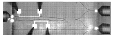
- FIG. 2 is a photomicrograph of the manufactured monolithic integrated optical gate switch observed from above. It can be seen that a Michelson interferometer, a variable light intensity attenuator, etc. are integrated in a device length of 1 mm.
- FIG. 3 is a photograph of the state when a TE-polarized continuous wave (CW) signal light having a wavelength of 1560 nm is input from the port 2 and taken with an infrared camera and a microscope. Images were taken under the condition that no current was passed through the heaters of the phase adjustment bias units 8 and 9. It can be confirmed that the signal light branched by the branching unit 5 reaches the end faces of the ports 3 and 4, and the signal light slightly converted into the radiation mode at the end faces appears to shine white. Furthermore, the light reflected from the ports 3 and 4 is multiplexed at the branching section 5 and then guided to the port 1. The signal light slightly converted into the radiation mode at the end face of the port 1 is lit white. This can be confirmed.
- CW TE-polarized continuous wave
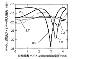
- FIG. 4 shows the static ON / OFF extinction characteristics of the prototype optical gate switch.
- the numbers in the figure are applied voltages (Volt) of the phase adjustment bias unit 9.
- TM polarization control light pulse repetition 10 GHz, wavelength 1545 nm, pulse width 2.4 ps, pulse energy 8.7 pJ
- TE polarization signal light CW, wavelength 1560 nm
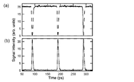
- 5A and 5B show the results of measuring the time waveform of the signal light returned to port 2 and the signal light output to port 1 and confirming the optical gate operation.
- FIG. 5A shows the signal light returned to the port 2
- FIG. 5B shows the signal light output to the port 1.
- a circulator was used to separate the signal light returning to port 2 from the input signal.
- an upward change FIG. 5
- the applied voltage of the phase adjustment bias unit 8 is adjusted to 3.45V.
- the most intense interference condition is obtained and the maximum signal intensity returns to the port 2.
- the output signal of the port 1 is the most destructive interference condition, and an optical signal with the minimum intensity close to 0 is output to the port 1.
- the time region showing the flat signal intensity corresponds to the time region in which the control light is not incident on the waveguide. Each corresponds to the strongest condition and the weakest condition.
- the time waveform in Fig. 5 (b) corresponds to the time response of the gate operation.
- the half width of the measured peak waveform is 3.2 ps.
- the half width of the input control light pulse is 2 ps, and the gate operation time is larger than the input width of the control light.
- This time lag is considered to be delayed by the amount of time required for electrons excited from the base subband to the upper subband due to intersubband transition to relax to the base subband. From the above, it was confirmed that the optical gate switch was operating due to the phase modulation effect caused by intersubband transition.
- an optical gate in a 160 Gb / s optical time multiplexed signal (40 Gb / s RZ (return-to-zero) signal is four-channel time multiplexed) required for an optical transmission system using an ultrafast optical time multiplexing system.
- the operation of the pulse train separation was performed by operating the switch and extracting one channel of the multiplexed signal.
- a 160 Gb / s signal (wavelength 1560 nm) is input from port 2 as TE polarization signal light, and TM polarization control light (wavelength 1545 nm, repetition 40 GHz, pulse width 2.4 ps, pulse energy 2.9 pJ) is transmitted from port 3. I input it.
- the applied voltage of the phase adjustment bias unit 8 was adjusted to 1.54 Volt so that the 160 Gb / s signal was not output from the port 2 when no control light was input.
- FIG. 6 shows a 40 Gb / s signal output from port 1 and separated from the pulse train.
- the light intensity is suppressed to the noise level, and it has been confirmed that only specific channels of the optical time division multiplexed signal are well separated. It was.
- Example 2 The second embodiment is an example in which the basic configuration of the first embodiment is further improved to reduce the propagation loss of the element with respect to the TE polarized signal light.
- FIG. 7 shows a structure for reducing a loss of signal light in a waveguide other than the phase modulation unit in the basic configuration diagram of the present invention (see FIG. 1).
- quantum well mixing is performed by phosphorus ion implantation and rapid annealing.
- the structure of Example 2 is manufactured in the same manner as in Example 1, but differs in the following steps.
- a mask is made of SiO 2 or the like in a region corresponding to the phase modulation unit 15 on a wafer for manufacturing an optical integrated circuit.
- a dose amount of 1 ⁇ 10 14 to 1 ⁇ 10 15 / cm 2 is implanted into a region other than the phase modulation unit 15, for example, with P or As ions.
- the energy of ions to be implanted is set so that the distribution of implanted ions in the depth direction has a peak near the center of the upper InP cladding layer.
- vacancies are implanted into the upper InP cladding layer crystal.
- the vacancies diffuse into the quantum well core layer below the upper cladding layer, thereby causing a transition between the sub-bands of the quantum well layer and the barrier layer. Atoms are mixed between them.
- the optical waveguide for connecting the branch portions 5 to 7, the attenuation portions 10 and 11, and the branch portion shown in FIG. 1 using a normal semiconductor process can be formed by a dry etching method.
- the phase modulation unit 15 is located in a partial region on the end face side of the phase modulation side arm of the Michelson interferometer.
- the core layer includes a phase modulation unit and a region having a characteristic in which the absorption edge wavelength of interband transition is shifted to a short wavelength.
- the phase modulation unit 15 can be 1/10 to 1, for example, about 1/2 the length of the phase modulation side arm of the Michelson interferometer.
- the length of the phase modulation unit connected to the port 3 is preferably set to a distance at which the TM wave incident from the end (port 3) of the phase modulation side arm is attenuated. Good.
- the region of the core layer having the characteristic that the absorption edge wavelength of the interband transition moves to a short wavelength is preferably the entire core layer other than the phase modulation unit from the viewpoint of reducing the propagation loss of the signal light. Even if it is a part, there is a reduction effect.
- Phase adjustment bias unit 8 9 Phase adjustment bias unit 9 10 Attenuator 10 11 Attenuator 11 12 Non-reflective film 12 13 Partial reflection film 13 14 Variable light intensity attenuation part 14 15 Phase modulator 15
Landscapes
- Physics & Mathematics (AREA)
- Nonlinear Science (AREA)
- Optics & Photonics (AREA)
- General Physics & Mathematics (AREA)
- Chemical & Material Sciences (AREA)
- Engineering & Computer Science (AREA)
- Nanotechnology (AREA)
- Life Sciences & Earth Sciences (AREA)
- Biophysics (AREA)
- Crystallography & Structural Chemistry (AREA)
- Optical Modulation, Optical Deflection, Nonlinear Optics, Optical Demodulation, Optical Logic Elements (AREA)
Abstract
Description
非特許文献3では、マイケルソン干渉計自体は光ファイバーやカプラにより構成されているのに対し、非特許文献4ではSOAの効果をもつ基板上にモノリシック集積化されている。これらの論文はSOAの光非線形性による位相変調効果を利用しており、サブバンド間遷移による位相変調効果を光集積化する際に必要となる技術の詳細については範囲外である。また干渉計の光路間の光強度のバランスを保つ機構が本発明と異なる。
この特許文献1では、Si細線導波路によるマイケルソン干渉計の反射側の一方のアームの光導波路と、位相変調効果を示すIII-V族半導体導波路を接続させることにより、位相変調部を干渉計内に導入している。信号光、制御光はともにSi細線導波路光回路側からバット接合部を通じて、III-V族半導体導波路へ導入されている。しかし、シリコン細線導波路とIII-V族半導体導波路の接続において、サブミクロン以下の位置合わせ精度が要求され、かつシリコン細線導波路とIII-V族半導体導波路の導波路モードサイズを一致させる方法が確立されておらず、実用上十分な光結合効率をとることは困難である。現在までのところ、このハイブリッド集積の形態をもつ実用的な光ゲートスイッチは実現されていない。
具体的には、ピエゾ素子をつけたミラーによる微動機構及びその位置安定化回路が必要であり、デバイス構成が複雑になるという問題点があった。また、多数の光ゲートスイッチを同時に動作させる必要がある場合、複数個の光ゲートスイッチを集積する必要がある。これまでの空間光学系の配置では、装置全体のサイズが大きくなるという問題点があった。
特許文献1で開示されたシリコン光細線とIII-V族半導体導波路をハイブリッド集積した光ゲートスイッチにおいては小型化が期待できるが、位相変調を発生させるIII-V族半導体導波路と、干渉計用の光集積回路との間の高い光結合効率を得るのが難しいという問題がある。接続部による光結合損により、位相変調を生じさせるのに必要な十分な制御光パワーが、III-V族半導体導波路に位相変調部に届かず、位相変調効率が落ちる。さらに信号光は、結合部を往復する必要があり、結合損が倍増する。以上により光ゲートで切り出された信号光に対して十分な信号/雑音比を得ることが困難である。
(1)サブバンド間遷移による位相変調効果を示す量子井戸をコア層とする光導波路ウエハと、該光導波路ウエハ上に形成されたマイケルソン干渉計と該マイケルソン干渉計反射側のアームの一方に干渉計の光バランスを調整するための可変光強度減衰部とを備えたことを特徴とする光ゲートスイッチ。
(2)上記コア層は、上記マイケルソン干渉計の位相変調用側アームの端面側の部分領域に位置する位相変調部と、バンド間遷移の吸収端波長が短波長へ移動した特性を有する領域とを、備えることを特徴とする(1)に記載の光ゲートスイッチ。
(3)上記マイケルソン干渉計の反射側のアームの端面に、制御光を導入できるように部分反射膜を形成したことを特徴とする(1)又は(2)に記載の光ゲートスイッチ。
(4)上記マイケルソン干渉計の信号光入出力側アーム端面に、無反射膜を形成したことを特徴とする(1)乃至(3)のいずれか1に記載の光ゲートスイッチ。
また、ポート3に接続される位相変調部15以外の部分は、PあるいはAsイオン注入と急速アニールにより量子井戸混合を生じさせ、バンド間遷移の吸収端波長を短波長化すると、素子の光損失が低減でき、信号対雑音比を高めることができる。
光ゲートスイッチの全体の構成は以下のとおりである。
(1)4つの入出力ポート(ポート1~4)と分岐部5によりマイケルソン干渉計を構成している。
(2)ポート1及び2は信号光入出力部であり、無反射膜12が設けられている。またポート3及び4は、信号光の反射部として働くと同時に、ポート3は制御光の入力部としての機能をもたせるために、部分反射膜13が設けられている。
(3)分岐部5とポート4との間には、分岐部6と7、位相調整バイアス部9、減衰部10、11から構成されたマッハーツェンダー干渉計からなる可変光強度減衰部14が設けられている。
(4)分岐部5とポート3との間には、位相変調用の干渉計アームとして動作すると同時に、マイケルソン干渉計の静的な位相調整バイアス部8が設けられている。
(5)分岐部6と7の間の光路のうちの一方には、光強度を可変減衰させるための位相調整バイアス部9が設けられている。
なおこの光ゲートスイッチ光集積回路のすべての分岐部は、TE偏波の信号光に対して3dB分岐として最適に動作するように、そのサイズが設計されている。
図7に本発明の光ゲートスイッチの改良された構成を示す。
(6)ポート3に接続される位相変調部15以外の部分は、PあるいはAsイオン注入と急速アニールにより量子井戸混合を生じさせて、バンド間遷移の吸収端波長を短波長化する。量子井戸混合の処理を行うことにより、TE偏波信号光が光回路中を伝搬するときに生じるバンド間遷移吸収による影響を避けることができる。このため素子の光損失が低減でき、信号対雑音比を高めることができる。
ポート1とポート2はそれぞれ信号入力部と出力部となるために、導波路端面はヘキカイにより形成されており、信号の反射損を抑制するために無反射膜が蒸着されている。
ポート1から入力されたTE偏波信号光は、分岐部5で等強度に分岐され、それぞれポート3及び4へと導かれる。
ポート3の導波路端面を部分反射膜とすることにより、TM偏波の制御光をポート3から導波路内へ導入することが可能となる。
ポート3から光導波路内に入力されたTM偏波制御光は、サブバンド間遷移吸収により急速に減衰する。このためポート3から分岐部5に至る光路内で、TM偏波制御光を完全に減衰することが理想である。この部分の光路の屈折率だけを変化させるように、光路長が設計されている。
したがって分岐部5において分岐され後、ポート3で反射して分岐部5に戻ってきたTE信号光は、TM偏波制御光により発生した屈折率変化の影響を受けて、位相変調効果を受けている。
ポート3及び4で反射されて分岐部5に戻ってきたTE偏波の信号は、分岐部5により再び合波されるが、干渉条件に応じてポート1あるいはポート2へ導かれる。
TM偏波制御光をポート3に入力すると、制御光がサブバンド間遷移により吸収され、熱に変換される。ポート3導波路端面からTM制御光が減衰する部分までの導波路において、この発熱は生じており、この部分の導波路の温度が上昇する。その結果、半導体量子井戸のバンド間遷移による吸収端が長波長側にシフトする。このような状況において、TE偏波信号光が量子井戸のバンド間遷移の吸収端よりわずかに長波に設定されている場合には、熱効果で長波長側へシフトした量子井戸のバンド間遷移吸収を受ける。発熱による効果は応答速度が遅く、10GHz程度以上の繰り返し光パルスの制御光に対して、ほとんど静的な振る舞いを示す。ポート3から反射して戻ってきた信号光のこの熱効果による静的な減衰は、マイケルソン干渉計のもう一方のアームから反射して戻ってきた光との間の光強度バランスをくずす。これは干渉度合いの低下により、光ゲートスイッチ動作時のON/OFF消光比の低下をもたらし、光ゲートスイッチ動作に支障をきたす。
モノリシック集積型の光ゲートスイッチを形成するための好ましい実施例について説明する。
光集積回路を形成するためのウエハとしては、サブバンド間遷移による位相変調効果を生じさせる量子井戸構造を容易に成長させるために、InP基板を用いる。
上記の光導波路用のウエハに対して、通常の半導体プロセスを用いて図1に示した分岐部5~7、減衰部10、11、分岐部をつなぐ接続用の光導波路をドライエッチング法により形成する。
可変強度減衰部14が正常に動作するためには、減衰部に導かれた信号光が効率よく減衰し、反射光として戻らないようにする必要がある。本実施例では、曲げ半径10μmのU字導波路を設けることにより、光導波路内の光を曲げ損失により外部へ放射させるようにした。またU字導波路の終端にU字導波路を終端まで伝搬した信号光を減衰させるために、U字導波路の終端にテーパー導波路を接続した。導波路の幅を1.6μmからモードカットオフサイズ以下の0.3μmまで断熱的に減少させて、信号光の減衰を図った。
その後、基板の裏面をラッピングにより100μm程度厚にまで薄くした後、デバイスチップをヘキカイにより切り出だす。ヘキカイ端面におけるポート1~4の反射率を調整するために、ECRスパッタ装置により誘電体膜の蒸着を行う。ECRスパッタ法による誘電体膜の蒸着に際して、まずECRスパッタ装置内でヘキカイ端面をArプラズマにさらして、端面の清浄化を行った後、誘電体膜の製膜を行うのが、密着性の観点から好ましい。
図2は、作製したモノリシック集積光ゲートスイッチを上部より観察した顕微鏡写真である。デバイス長1mmの中に、マイケルソン干渉計、可変光強度減衰部等が集積されている様子がわかる。
実施例に従って、作製したモノリシック集積型光ゲートスイッチの特性について説明する。
図3は、ポート2より波長1560nmのTE偏波の連続波(CW)信号光を入力したときの様子を、赤外カメラと顕微鏡により撮影したとき写真である。位相調整バイアス部8、9のヒーターには電流を流していない条件で撮影した。
分岐部5で分岐された信号光が、ポート3及び4の端面まで到達し、端面でわずかに放射モードに変換された信号光が白く光って見えているのが確認できる。
さらに、ポート3、4から反射した光が、分岐部5で合波された後、ポート1へ導かれていることが、ポート1の端面でわずかに放射モードに変換された信号光が白く光っていることにより、確認できる。
図4に、試作した光ゲートスイッチの静的ON/OFF消光特性を示す。図中内の数字は、位相調整バイアス部9の印加電圧(Volt)である。可変光減衰器内の位相バイアス調整部9の電圧が0のとき(減衰量が0)、位相調整バイアス部8の電圧を変化させると、24dBの強度変化が得られた。このことより、光ゲートスイッチの静的ON/OFF消光比が、通常の用途で要求される値(~20dB程度)をクリアする性能であることを示している。
図5において、100psおきにTM制御光がポート3に入射されたタイミングに応じて、ポート1より出力されたTE偏波信号光の光強度に上向きの変化(図5(b))が生じている。また図5(a)に示すように、ポート2に戻ってきた信号光には下向きの変化が生じている。
上記の干渉条件に保持した状態で、制御光パルスがポート3へ入力され、サブバンド間遷移により導波路内で吸収されると、位相変調効果により、位相変調用アーム側で反射される信号光の位相が、最大でπラジアンだけシフトする。このため、ポート2においては、干渉条件が最も弱め合う状態へと変化し、信号強度が0近くにまで減少する。その後、制御光により生じた位相変調効果が消滅すると、信号光は元の最大強度の状態へと回復する。このため、図5(a)において、下向きのパルス状の光信号強度変化が観測されている。一方、ポート1では、ポート2とは正反対の光強度の時間変化を示す。すなわち制御光パルスが入射されると、最も強め合う干渉条件へと変化し、制御光パルスの入射と同期して、最大強度の信号光が出力される。このため、図5(b)では上向きのパルス状の光強度変化が観測されている。
実施例2は、実施例1の基本構成において、さらに、TE偏波信号光に対する素子の伝搬損失を低減するための改良を行った例である。図7を参照して説明する。図7に、本発明の基本構成図(図1参照)において、位相変調部以外の導波路の信号光に対する損失を低減するための構造を示す。図7の位相変調部15の領域以外を、燐イオン注入と急速アニールにより量子井戸混合を生じさせることを行う。実施例2の構造は、実施例1と同様に製造するが、次の工程で異なる。光集積回路作製のためのウエハ上の、位相変調部15に相当する領域にSiO2等によりマスクを作製する。次に、位相変調部15以外の領域に、たとえばPあるいはAsイオンを、ドーズ量1×10¹⁴~1×10¹⁵/cm2注入する。注入するイオンのエネルギーは、注入イオンの深さ方向の分布が、上部InPクラッド層の中央部付近においてピークを持つように設定する。このイオン注入に伴い上部InPクラッド層結晶中に空孔が注入される。その後、700~800℃に急速に加熱しアニールすることにより、空孔が上部クラッド層より下部にある量子井戸コア層へ拡散することにより、サブバンド間遷移を生じさせる量子井戸層と障壁層の間で原子が混合される。このことにより、バンド間遷移の吸収端波長が短波長へ移動し、信号光の伝搬損失を低減することが可能になる。上記のイオン注入と急速アニールにより量子井戸混合を生じさせる工程の後、通常の半導体プロセスを用いて図1に示した分岐部5~7、減衰部10、11、分岐部をつなぐ接続用の光導波路をドライエッチング法により形成することができる。
2 ポート2
3 ポート3
4 ポート4
5 分岐部5
6 分岐部6
7 分岐部7
8 位相調整バイアス部8
9 位相調整バイアス部9
10 減衰部10
11 減衰部11
12 無反射膜12
13 部分反射膜13
14 可変光強度減衰部14
15 位相変調部15
Claims (4)
- サブバンド間遷移による位相変調効果を示す量子井戸をコア層とする光導波路ウエハと、該光導波路ウエハ上に形成されたマイケルソン干渉計と、該マイケルソン干渉計反射側のアームの一方に干渉計の光バランスを調整するための可変光強度減衰部とを備えたことを特徴とする光ゲートスイッチ。
- 上記コア層は、上記マイケルソン干渉計の位相変調用側アームの端面側の部分領域に位置する位相変調部と、バンド間遷移の吸収端波長が短波長へ移動した特性を有する領域とを、備えることを特徴とする請求項1記載の光ゲートスイッチ。
- 上記マイケルソン干渉計の反射側のアームの端面に、制御光を導入できるように部分反射膜を形成したことを特徴とする請求項1又は2に記載の光ゲートスイッチ。
- 上記マイケルソン干渉計の信号光入出力側アーム端面に、無反射膜を形成したことを特徴とする請求項1乃至3のいずれか1項に記載の光ゲートスイッチ。
Priority Applications (3)
| Application Number | Priority Date | Filing Date | Title |
|---|---|---|---|
| CN201280009046.9A CN103392149B (zh) | 2011-02-18 | 2012-02-15 | 光闸开关 |
| JP2012557984A JP5728693B2 (ja) | 2011-02-18 | 2012-02-15 | 光ゲートスイッチ |
| US13/985,699 US9002146B2 (en) | 2011-02-18 | 2012-02-15 | Optical gate switch |
Applications Claiming Priority (2)
| Application Number | Priority Date | Filing Date | Title |
|---|---|---|---|
| JP2011-033397 | 2011-02-18 | ||
| JP2011033397 | 2011-02-18 |
Publications (1)
| Publication Number | Publication Date |
|---|---|
| WO2012111689A1 true WO2012111689A1 (ja) | 2012-08-23 |
Family
ID=46672604
Family Applications (1)
| Application Number | Title | Priority Date | Filing Date |
|---|---|---|---|
| PCT/JP2012/053467 Ceased WO2012111689A1 (ja) | 2011-02-18 | 2012-02-15 | 光ゲートスイッチ |
Country Status (4)
| Country | Link |
|---|---|
| US (1) | US9002146B2 (ja) |
| JP (1) | JP5728693B2 (ja) |
| CN (1) | CN103392149B (ja) |
| WO (1) | WO2012111689A1 (ja) |
Cited By (1)
| Publication number | Priority date | Publication date | Assignee | Title |
|---|---|---|---|---|
| JPWO2016031096A1 (ja) * | 2014-08-27 | 2017-06-22 | 日本電気株式会社 | 光素子、終端器、波長可変レーザ装置及び光素子の製造方法 |
Families Citing this family (3)
| Publication number | Priority date | Publication date | Assignee | Title |
|---|---|---|---|---|
| JP6759739B2 (ja) * | 2016-06-13 | 2020-09-23 | 富士通オプティカルコンポーネンツ株式会社 | 光デバイス、波長可変光源、及びこれを用いた光送信器 |
| JP6870813B2 (ja) * | 2016-08-17 | 2021-05-12 | 国立大学法人 東京大学 | Mos型光変調器及びその製造方法 |
| US10244297B1 (en) | 2018-03-14 | 2019-03-26 | Juniper Networks, Inc. | Reduced crosstalk photonic switch |
Family Cites Families (7)
| Publication number | Priority date | Publication date | Assignee | Title |
|---|---|---|---|---|
| JPS6371826A (ja) * | 1986-09-16 | 1988-04-01 | Hitachi Ltd | 光半導体装置 |
| US5754714A (en) * | 1994-09-17 | 1998-05-19 | Kabushiki Kaisha Toshiba | Semiconductor optical waveguide device, optical control type optical switch, and wavelength conversion device |
| EP0744648A1 (en) * | 1995-05-25 | 1996-11-27 | Hitachi Europe Limited | Apparatus and method for coherently controlling an optical transition |
| GB2371406A (en) * | 2001-01-23 | 2002-07-24 | Univ Glasgow | An Optically Active Device |
| US6856737B1 (en) * | 2003-08-27 | 2005-02-15 | Mesophotonics Limited | Nonlinear optical device |
| JP4911404B2 (ja) * | 2006-08-25 | 2012-04-04 | 独立行政法人産業技術総合研究所 | 光信号処理回路 |
| JP5605621B2 (ja) | 2010-06-28 | 2014-10-15 | 独立行政法人産業技術総合研究所 | 光ゲートスイッチ |
-
2012
- 2012-02-15 CN CN201280009046.9A patent/CN103392149B/zh not_active Expired - Fee Related
- 2012-02-15 WO PCT/JP2012/053467 patent/WO2012111689A1/ja not_active Ceased
- 2012-02-15 US US13/985,699 patent/US9002146B2/en active Active
- 2012-02-15 JP JP2012557984A patent/JP5728693B2/ja not_active Expired - Fee Related
Non-Patent Citations (2)
| Title |
|---|
| AKIMOTO, R. ET AL.: "All-Optical Wavelength Conversion at 40Gb/s with Enhanced XPM by Facet Reflection using Intersubband Transition in InGaAs/AlAsSb Quantum Well Waveguide", ECOC 2010, September 2010 (2010-09-01), pages 1 - 3 * |
| SHOJI, Y. ET AL.: "Michelson Interferometer of Si-Wire Wavegude for Hybrid Integrated Devices", OECC 2010, July 2010 (2010-07-01), pages 868 - 869 * |
Cited By (1)
| Publication number | Priority date | Publication date | Assignee | Title |
|---|---|---|---|---|
| JPWO2016031096A1 (ja) * | 2014-08-27 | 2017-06-22 | 日本電気株式会社 | 光素子、終端器、波長可変レーザ装置及び光素子の製造方法 |
Also Published As
| Publication number | Publication date |
|---|---|
| CN103392149B (zh) | 2016-04-06 |
| US20130343694A1 (en) | 2013-12-26 |
| CN103392149A (zh) | 2013-11-13 |
| US9002146B2 (en) | 2015-04-07 |
| JP5728693B2 (ja) | 2015-06-03 |
| JPWO2012111689A1 (ja) | 2014-07-07 |
Similar Documents
| Publication | Publication Date | Title |
|---|---|---|
| Heck et al. | Hybrid silicon photonic integrated circuit technology | |
| USRE48379E1 (en) | Electronic-integration compatible photonic integrated circuit and method for fabricating electronic-integration compatible photonic integrated circuit | |
| US8483521B2 (en) | Cavity dynamics compensation in resonant optical modulators | |
| US9615152B2 (en) | Optical element and light receiving device | |
| KR100326582B1 (ko) | 비선형광학특성을갖는도파관을구비한광학장치 | |
| Skogen et al. | Monolithically integrated active components: a quantum-well intermixing approach | |
| US20120207428A1 (en) | Methods and systems for reducing polarization dependent loss | |
| US20130235890A1 (en) | Tunable hybrid laser with carrier-induced phase control | |
| JP6318468B2 (ja) | 導波路型半導体受光装置及びその製造方法 | |
| US11435522B2 (en) | Grating coupled laser for Si photonics | |
| WO2013055384A1 (en) | Gain medium providing laser and amplifier functionality to optical device | |
| CN105281200A (zh) | 基于rec技术的集成高速数字调制wdm-pon光模块 | |
| JP3616229B2 (ja) | 単一ポート光変調装置およびその装置を含む集積回路および光変調器を動作させる方法 | |
| JP5728693B2 (ja) | 光ゲートスイッチ | |
| US20220173572A1 (en) | Optical system and method for locking a wavelength of a tunable laser | |
| JP5228778B2 (ja) | 光回路素子 | |
| US11624943B2 (en) | Carrier injector having increased compatibility | |
| JP2011181789A (ja) | 半導体光源 | |
| US6512860B2 (en) | Bent electro-absorption modulator | |
| JP2005249973A (ja) | 波長フィルタ及び波長可変フィルタ | |
| JP2010211099A (ja) | 光フィルタ | |
| Wu et al. | Compact photonic integrated spatial mode controller based on thin film lithium niobate | |
| Wang et al. | Tunable Optical Delay Line Based on SOI Contradirectional Couplers with Sidewall-Rnodulated Bragg Gratings | |
| Akimoto et al. | Monolithically integrated ultrafast all-optical switch consisting of intersubband optical nonlinear waveguide and Michelson interferometer | |
| JP2025025671A (ja) | 混合変調レーザ |
Legal Events
| Date | Code | Title | Description |
|---|---|---|---|
| WWE | Wipo information: entry into national phase |
Ref document number: 201280009046.9 Country of ref document: CN |
|
| 121 | Ep: the epo has been informed by wipo that ep was designated in this application |
Ref document number: 12746569 Country of ref document: EP Kind code of ref document: A1 |
|
| ENP | Entry into the national phase |
Ref document number: 2012557984 Country of ref document: JP Kind code of ref document: A |
|
| NENP | Non-entry into the national phase |
Ref country code: DE |
|
| WWE | Wipo information: entry into national phase |
Ref document number: 13985699 Country of ref document: US |
|
| 122 | Ep: pct application non-entry in european phase |
Ref document number: 12746569 Country of ref document: EP Kind code of ref document: A1 |