WO2012108145A1 - 無線機器用アンテナ - Google Patents
無線機器用アンテナ Download PDFInfo
- Publication number
- WO2012108145A1 WO2012108145A1 PCT/JP2012/000656 JP2012000656W WO2012108145A1 WO 2012108145 A1 WO2012108145 A1 WO 2012108145A1 JP 2012000656 W JP2012000656 W JP 2012000656W WO 2012108145 A1 WO2012108145 A1 WO 2012108145A1
- Authority
- WO
- WIPO (PCT)
- Prior art keywords
- antenna
- conductor
- plate
- antenna elements
- raising
- Prior art date
- Legal status (The legal status is an assumption and is not a legal conclusion. Google has not performed a legal analysis and makes no representation as to the accuracy of the status listed.)
- Ceased
Links
Images



Classifications
-
- H—ELECTRICITY
- H01—ELECTRIC ELEMENTS
- H01Q—ANTENNAS, i.e. RADIO AERIALS
- H01Q21/00—Antenna arrays or systems
- H01Q21/06—Arrays of individually energised antenna units similarly polarised and spaced apart
- H01Q21/08—Arrays of individually energised antenna units similarly polarised and spaced apart the units being spaced along or adjacent to a rectilinear path
- H01Q21/12—Parallel arrangements of substantially straight elongated conductive units
-
- H—ELECTRICITY
- H01—ELECTRIC ELEMENTS
- H01Q—ANTENNAS, i.e. RADIO AERIALS
- H01Q21/00—Antenna arrays or systems
- H01Q21/28—Combinations of substantially independent non-interacting antenna units or systems
-
- H—ELECTRICITY
- H01—ELECTRIC ELEMENTS
- H01Q—ANTENNAS, i.e. RADIO AERIALS
- H01Q1/00—Details of, or arrangements associated with, antennas
- H01Q1/48—Earthing means; Earth screens; Counterpoises
-
- H—ELECTRICITY
- H01—ELECTRIC ELEMENTS
- H01Q—ANTENNAS, i.e. RADIO AERIALS
- H01Q1/00—Details of, or arrangements associated with, antennas
- H01Q1/52—Means for reducing coupling between antennas; Means for reducing coupling between an antenna and another structure
-
- H—ELECTRICITY
- H01—ELECTRIC ELEMENTS
- H01Q—ANTENNAS, i.e. RADIO AERIALS
- H01Q9/00—Electrically-short antennas having dimensions not more than twice the operating wavelength and consisting of conductive active radiating elements
- H01Q9/04—Resonant antennas
- H01Q9/0407—Substantially flat resonant element parallel to ground plane, e.g. patch antenna
- H01Q9/0421—Substantially flat resonant element parallel to ground plane, e.g. patch antenna with a shorting wall or a shorting pin at one end of the element
Definitions
- the present disclosure relates to an antenna for a wireless device that can satisfactorily transmit and receive radio waves in the entire circumferential direction, and more particularly to an antenna for a wireless device suitable for in-vehicle use.
- a shield plate for shielding a transmission / reception circuit for a wireless device is a GND plate, and a radiation plate parallel to the GND plate is disposed via a short-circuit conductor.
- an inverted F-type antenna having a shield plate as a GND plate is configured, and a diversity antenna is configured by arranging a plurality of the inverted F-type antennas in different directions.
- a nearly omnidirectional antenna could be realized by the directivity obtained by combining the directivity of a plurality of antennas.
- the present disclosure has been made in view of such problems, and an object thereof is to provide an antenna for a wireless device that can satisfactorily transmit and receive radio waves in the entire circumferential direction even when a conductive object is present in the vicinity.
- a wireless device antenna installed in the vicinity of a conductive object, the wireless device including a GND plate, a conductor plate, two antenna elements, and two raising conductor plates.
- a device antenna is provided.
- the GND plate is a conductor formed in a plate shape, and the potential is kept at the GND level.
- the conductor plate is disposed in parallel to the GND plate.
- Each antenna element is a monopole antenna element having a short-circuit conductor disposed on the conductor plate so as to be electrically connected to the conductor plate, and a radiation plate for radiating radio waves disposed at the tip of the short-circuit conductor It is.
- the two antenna elements are arranged substantially parallel to the side surface of the conductive object at an interval of a half wavelength of radio waves to be transmitted and received.
- the two raising conductor plates are provided between the GND plate and the previous conductor plate, and are disposed in the vicinity of the two antenna elements, respectively, and the conductor plate is raised to a predetermined height from the GND plate. Raise it.
- radio waves in all directions can be transmitted and received satisfactorily even when a conductive object is present in the vicinity.
- FIG. 1 is a configuration diagram showing a schematic configuration of a radio device antenna.
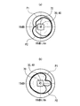
- FIG. 2A is a diagram illustrating a result of obtaining a current distribution flowing through the antenna element and the conductive object in the comparative example by simulation
- FIG. 2B is a current distribution flowing through the antenna element and the conductive object in the embodiment. It is a figure which shows the result calculated
- Fig.3 (a) is a figure which shows the directivity of the antenna of a comparative example
- FIG.3 (b) is a figure which shows the directivity of the antenna for radio
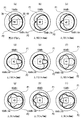
- FIGS. 4 (a) to 4 (i) are diagrams showing the directivity of the radio device antenna when the distance between the conductor plates for raising is changed.
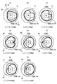
- FIGS. 5 (a) to 5 (h) are diagrams showing the directivity of the radio device antenna when the length of the raising conductor plate is changed.
- FIGS. 6A to 6C are diagrams showing the directivity of the radio device antenna when the length of the raising conductor plate is changed.
- FIG. 1 is a configuration diagram illustrating a schematic configuration of a radio device antenna 1.
- the radio device antenna 1 includes a GND board 10, a printed circuit board 20, antenna elements 30 and 40, and raising conductor plates 50 and 60, and is installed in the vicinity of the conductive object 70.
- the conductive object 70 is a conductor such as a metal structure, for example, a telematics antenna installed on the roof or bonnet of the vehicle body. That is, when the plurality of antennas including the wireless device antenna 1 are gathered in a narrow space to form a compact shape, an antenna other than the wireless device antenna 1 is an example of the conductive object 70.
- the GND plate 10 is a conductor plate made of metal such as a copper plate formed in a substantially rectangular plate shape.
- the GND board 10 is grounded so that its potential is maintained at the GND level.
- the printed circuit board 20 is formed in a substantially rectangular plate shape.
- the printed circuit board 20 is arranged so that the longitudinal direction of the printed circuit board 20 is parallel to the side surface of the conductive object 70 and the plate surface of the printed circuit board 20 is parallel to the GND board 10.
- the printed circuit board 20 is formed with a conductor pattern that conducts between the two antenna elements 30 and 40.
- the printed circuit board 20 is provided with an electronic circuit for mounting the semiconductor integrated circuit chip or the electronic component and operating the antenna 1 for the wireless device.
- the conductor pattern for comprising may be formed.
- the antenna elements 30 and 40 are arranged at both corners on the side far from the conductive object 70 on the printed circuit board 20.
- the two antenna elements 30 and 40 are inverted F type antennas which are a kind of monopole type antennas.
- the short-circuit conductors 32 and 42 are electrically connected to the conductor pattern of the antenna element on the printed circuit board 20 so as to be substantially perpendicular to the plate surface of the printed circuit board 20.
- radiation plates 34 and 44 are attached to the tips of the short-circuit conductors 32 and 42 so as to be parallel to the printed circuit board 20.
- plate-like feed conductors 36 and 46 are attached to the radiation plates 34 and 44 of the antenna elements 30 and 40 so that the tip portions thereof are not in contact with the GND plate 10 so as to be parallel to the short-circuit conductor 32.
- the tips of the feeding conductors 36 and 46 of the antenna elements 30 and 40 are used as feeding points, and a 5 GHz transmission signal is fed between the feeding point and the GND plate 10.
- the distance between the feeding points of the two antenna elements 30 and 40 is larger than the width of the conductive object 70, and the distance from the feeding point of the two antenna elements 30 and 40 to the conductive object 70 is half of the radio wave to be transmitted and received. It is arranged to be within the wavelength.
- the raising conductor plates 50 and 60 are two conductor plates formed in a substantially rectangular shape.
- the raising conductor plates 50 and 60 are conductor plates for raising the printed board 20 from the GND plate 10 to a height of 1/16 wavelength or more of radio waves to be transmitted and received.
- the two raising conductor plates 50 and 60 are attached between the GND board 10 and the printed circuit board 20, and their longitudinal ends are attached to the short direction ends of the printed circuit board 20.
- antenna 1 for wireless device In the radio device antenna 1 configured as described above, a printed circuit board 20 as a conductor plate is disposed in parallel with the GND plate 10.
- Two antenna elements 30 and 40 are arranged on the printed circuit board 20 at intervals of a half wavelength.
- the printed circuit board 20 is raised from the GND board 10 by 1/16 wavelength or more by the raising conductor plates 50 and 60. Further, the radio device antenna 1 is placed in the vicinity of the conductive object 70 so that the two antenna elements 30 and 40 are substantially parallel to the side surface of the conductive object 70.
- a current loop of approximately one wavelength is formed between the GND board 10, the printed board 20, and the two raising conductor plates 50 and 60 with respect to the transmission signal supplied from the feeding point. That is, the current path formed on the printed circuit board 20 between the two antenna elements 30 and 40, the current path formed on the two raising conductor plates 50 and 60, the current path formed by the GND board 10, and the A substantially one-wave current loop is formed which consists of a mirror image of the current path.
- the antenna can satisfactorily transmit and receive radio waves in the entire circumferential direction.
- the distance between the two antenna elements 30 and 40 is made larger than the width of the conductive object 70, and the distance from the feeding point of the two antenna elements 30 and 40 to the conductive object 70 is half of the radio wave to be transmitted and received. It is arranged to be within the wavelength.
- FIGS. 2 (a) and 2 (b) show the results obtained by simulating the distribution of current flowing through the antenna elements 30 and 40 and the conductive object 70 when a transmission signal of 5 GHz is applied to the feeding point of the antenna element 40.
- the direction of the current is indicated by an arrow
- the sparse / dense current distribution is indicated by the sparse / dense arrow distribution. That is, the current distribution is sparse in the portion where the arrow distribution is sparse, and the current distribution is dense in the portion where the arrow distribution is dense.
- the distribution of arrows in the lower right part of the conductive object 70 is denser than the other parts. That is, it can be seen that the current distribution in the lower right portion of the conductive object 70 is dense, and the current distribution in the conductive object 70 is not uniform.
- 3 (a) and 3 (b) show the antenna and the comparison example obtained by simulation when the radiated radio wave is 5 GHz and the height of the raising conductor plates 50 and 60 is ⁇ / 12. It is a figure which shows the directivity of the antenna 1 for radio
- the power supply point of the other antenna element 40 is connected to the conductor pattern of the printed circuit board 20 through a 50 ⁇ termination resistor.
- the wireless device antenna 1 (antenna elements 30 and 40) and the conductive object 70 are placed at the center, and the dashed curve indicated by P1 in FIG. The directivity of the element 30 is shown, and the solid curve indicated by P2 shows the directivity of the antenna element 40.
- FIG. 3 (a) shows the directivity of the antenna of the comparative example
- FIG. 3 (b) shows the directivity of the wireless device antenna 1 of the present embodiment.
- the directivity in the antenna of the comparative example is the directivity in the direction of the conductive object 70 even if the directivity P1 of the antenna element 30 and the directivity P2 of the antenna element 40 complement each other. It is falling.
- the radio device antenna 1 of the present embodiment as shown in FIG. 3B, as a result of complementation of P ⁇ b> 1 and P ⁇ b> 2, directivity is reduced with respect to the direction of the conductive object 70. Absent. That is, it can be seen that the wireless device antenna 1 of the present embodiment shows better directivity in the entire circumferential direction than the antenna of the comparative example.
- FIGS. 4 (a) to 4 (i) are diagrams showing the relationship between the height of the conductor plates 50 and 60 for raising and the directivity.
- FIG. 4 (a) shows the directivity of the antenna (the antenna of the comparative example) when there is no conductive plate 50, 60 for raising.
- 4 (b) to 4 (i) the heights of the conductor plates 50 and 60 for raising are set to ⁇ / 50, ⁇ / 25, ⁇ / 16, ⁇ / 12, The directivity of the wireless device antenna 1 when ⁇ / 10, ⁇ / 8, ⁇ / 7, and ⁇ / 6 is shown.
- the directivities shown in FIGS. 4B and 4C are not so different from the directivities shown in FIG. 4A, and even if P1 and P2 complement each other, they are directed toward the conductive object 70. There is a part where the sex decreases.
- the directivity shown in FIGS. 4D to 4I does not have a portion in which directivity decreases in the direction of the conductive object 70 by complementing P1 and P2, and FIG. It can be seen that better directivity is obtained in the entire circumferential direction than the directivity shown in FIG.
- the raising conductor plates 50 and 60 have a height of ⁇ / 16 or more, the directivity in the entire circumferential direction is improved.
- FIGS. 5 (a) to 5 (h) are diagrams showing the directivity of the radio device antenna 1 when the distance between the conductor plates 50 and 60 for raising is changed when a radio wave of 5 GHz is radiated. .
- the intervals between the raising conductor plates 50 and 60 are respectively set to ⁇ / 1, 9, ⁇ / 2, ⁇ / 2.2, ⁇ / 2.4, ⁇ /
- the directivity of the radio device antenna 1 when 2.7, ⁇ / 3, ⁇ / 3.4, and ⁇ / 3.9 is shown.
- 5A to 5H the height of the raising conductor plates 50 and 60 is ⁇ / 12.
- 6 (a) to 6 (c) are diagrams showing the directivity of the radio device antenna 1 when the lengths of the raising conductor plates 50 and 60 are changed when a radio wave of 5 GHz is radiated. is there.
- 6 (a) to 6 (c) show the directivity of the antenna 1 for radio equipment when the lengths of the conductive plates 50 and 60 for raising are 15 mm, 11.25 mm, and 7.5 mm, respectively. Yes.
- the antenna 1 for a radio device can be made shorter in height direction than other monopole type antennas. Therefore, it can be set as the antenna 1 for radio
- the radio device antenna 1 can be reduced in size.
- the raising conductive plate 60 is made the same as the length of the printed board 20 in the short direction. However, the same performance can be obtained if the conductor plate 60 for raising is longer than half the length of the printed circuit board 20 in the short direction.
- a wireless device antenna (1) installed in the vicinity of a conductive object (70) includes a GND plate (10), a conductor plate (20), and two antenna elements.
- an antenna for a wireless device including (30, 40) and two raising conductor plates (50, 60).
- the GND plate (10) is a conductor formed in a plate shape, and the potential is kept at the GND level.
- the conductor plate (20) is a conductor plate arranged in parallel to the GND plate (10).
- Each antenna element (30, 40) includes a short-circuit conductor (32, 42) disposed on the conductor plate (20) so as to be electrically connected to the conductor plate (20), and the short-circuit conductor (32, 42). It is a monopole antenna having radiation plates (34, 44) for radiating radio waves arranged at the tip.
- the two antenna elements (30, 40) are arranged approximately parallel to the side surface of the conductive object (70) at an interval of a half wavelength of radio waves to be transmitted and received.
- the two raising conductor plates (50, 60) are arranged between the GND plate (10) and the conductor plate (20) and in the vicinity of each of the two antenna elements (30, 40).
- the conductor plate (20) is a plate of two conductors for raising the conductor plate (20) from the GND plate (10) to a predetermined height.
- Such a radio device antenna (1) is an antenna that can satisfactorily transmit and receive radio waves in all directions even when a conductive object (70) is present in the vicinity. This will be described below.
- the conductor plate (20) is arranged in parallel to the GND plate (10), and two antenna elements (30, 40) are disposed on the conductor plate (20, 40) at half-wavelength intervals.
- the conductor plate (20) is raised to a predetermined height from the GND plate (10) by the raising conductor plates (50, 60).
- the radio device antenna (1) is placed in the vicinity of the conductive object (70) so that the two antenna elements (30, 40) are substantially parallel to the side surface of the conductive object (70).
- This current path is formed by the half-wavelength current path 1 between the two antenna elements (30, 40) formed on the conductor plate (20) and the two raising conductor plates (50, 60).
- the current path 2 and the mirror image formed by the GND plate (10) have a wavelength twice the sum of the current path 1 and the current path 2.
- the current loop acts as a new wave source
- the current distribution of the current induced in the conductive object (70) changes.
- the phase relationship between the currents flowing through the two antenna elements (30, 40) and the conductive object (70) changes, so that the directivity of the radio waves radiated from the two antenna elements (30, 40) is the same. Changes, and the directivity of the wireless device antenna (1) is complemented.
- the wireless device antenna (1) is an antenna that can satisfactorily transmit and receive radio waves in all directions.
- the transmission signal supplied to the antenna element (30, 40) is within a range where the conductive signal (20) can be conducted.
- Near each of the two antenna elements (30, 40) means that the distance between the two antenna elements (30, 40) and the conductor plate (20) is within a range where the above-described current loop is formed. It means that there is.
- the conductor plate (20) is raised from the GND plate (10) by the raising conductor plates (50, 60), a current loop is formed. It becomes the antenna (1) for radio
- the predetermined height of the raising conductor plate (50, 60) is set to 1/16 wavelength or more of radio waves to be transmitted and received, radio waves in the entire circumferential direction can be transmitted and received better.
- the distance between the two antenna elements (30, 40) is made larger than the width of the conductive object (70), and the distance from the feeding point of the two antenna elements (30, 40) to the conductive object (70).
- the monopole antenna elements (30, 40) include various antennas such as a monopole antenna and an L antenna.
- the monopole antenna element (30, 40) may be an inverted F antenna. According to this structure, it can be set as the radio
- the conductor plate (20) may be a printed board on which a conductor pattern for conducting at least between the two antenna elements (30, 40) is formed. According to this configuration, in addition to the conductor pattern that conducts between the two antenna elements (30, 40), by forming other conductor patterns, various circuit elements can be arranged on the conductor plate (20), and electronic Since the circuit can be formed, the antenna (1) for the wireless device can be reduced in size.
Landscapes
- Variable-Direction Aerials And Aerial Arrays (AREA)
- Details Of Aerials (AREA)
- Waveguide Aerials (AREA)
Abstract
Description
(無線機器用アンテナ1の構成)
図1は、無線機器用アンテナ1の概略の構成を示す構成図である。無線機器用アンテナ1は、GND板10、プリント基板20、アンテナエレメント30,40及びかさ上げ用導体板50,60を備えており、導電物体70の近傍に設置されている。
(無線機器用アンテナ1の作用)
以上のように構成された無線機器用アンテナ1では、GND板10に平行に、導体板としてのプリント基板20を配置する。プリント基板20の上に2分の1波長の間隔で2つのアンテナエレメント30,40を配置する。プリント基板20をかさ上げ用導体板50,60でGND板10から16分の1波長以上かさ上げする。さらに、2つのアンテナエレメント30,40が導電物体70の側面と略平行になるように、無線機器用アンテナ1を導電物体70の近傍に置くようにしてある。
(その他の実施形態]
上記実施形態では、かさ上げ用導体板60をプリント基板20の短手方向の長さと同じにした。しかし、かさ上げ用導体板60をプリント基板20の短手方向の長さの2分の1以上の長さであれば、同じ性能を得ることができる。
(様態)
本開示の無線機器用アンテナは、様々な様態を有する。例えば、本開示の一様態によると、導電物体(70)の近傍に設置される無線機器用アンテナ(1)であって、GND板(10)と、導体板(20)と、2つのアンテナエレメント(30,40)と、2つのかさ上げ用導体板(50,60)とを備える無線機器用アンテナが提供される。
「2つのアンテナエレメント(30,40)それぞれの近傍」とは、2つのアンテナエレメント(30,40)と導体板(20)の間の距離が、前述の電流ループが形成される程度の範囲内にあることを意味している。
Claims (5)
- 導電物体(70)の近傍に設置される無線機器用アンテナであって、
板状に形成された導体であって、電位がGNDレベルに保たれたGND板(10)と、
前記GND板(10)に平行に配置された導体板(20)と、
2つのアンテナエレメント(30、40)と、
2つのかさ上げ用導体板(50、60)と、
を備え、
各アンテナエレメント(30、40)は、前記導体板(20)と導通するように該導体板(20)上に配置された短絡導体(32、42)と、該短絡導体(32、42)の先端に配置される電波を放射するための放射板(34,44)と、を有するモノポール型アンテナエレメントであり、
前記2つのアンテナエレメント(30、40)は、送受信する電波の2分の1波長の間隔で、前記導電物体(70)の側面と略平行に配置され、
前記2つのかさ上げ用導体板(50、60)は、前記GND板(10)と前記導体板(20)との間に設けれ、前記2つのアンテナエレメント(30,40)それぞれの近傍に配置され、前記導体板(20)を前記GND板(10)から、所定の高さにかさ上げする無線機器用アンテナ。 - 請求項1に記載の無線機器用アンテナにおいて、
前記2つのかさ上げ用導体板(50、60)による所定の高さは、
送受信する電波の16分の1波長以上である無線機器用アンテナ。 - 請求項1又は請求項2に記載の無線機器用アンテナにおいて、
前記2つのアンテナエレメント(30、40)間の距離は、前記導電物体(70)の幅より大きく、
前記2つのアンテナエレメント(30、40)は、当該2つのアンテナエレメント(30、40)の給電点から前記導電物体までの距離が、送受信する電波の2分の1波長以内であるように配置されている無線機器用アンテナ。 - 請求項1~請求項3のいずれか1項に記載の無線機器用アンテナにおいて、
各モノポール型のアンテナエレメントは、逆F型アンテナである無線機器用アンテナ。 - 請求項1~請求項4のいずれか1項に記載の無線機器用アンテナにおいて、
前記導体板(20)は、
少なくとも、前記2つのアンテナエレメント(30、40)間を導通させる導体パターンが形成されたプリント基板(20)である無線機器用アンテナ。
Priority Applications (2)
| Application Number | Priority Date | Filing Date | Title |
|---|---|---|---|
| US13/997,849 US9059518B2 (en) | 2011-02-08 | 2012-02-01 | Antenna for wireless apparatus |
| DE112012000716T DE112012000716T5 (de) | 2011-02-08 | 2012-02-01 | Antenne für eine Funkvorrichung |
Applications Claiming Priority (2)
| Application Number | Priority Date | Filing Date | Title |
|---|---|---|---|
| JP2011025108A JP5368493B2 (ja) | 2011-02-08 | 2011-02-08 | 無線機器用アンテナ |
| JP2011-025108 | 2011-02-08 |
Publications (1)
| Publication Number | Publication Date |
|---|---|
| WO2012108145A1 true WO2012108145A1 (ja) | 2012-08-16 |
Family
ID=46638372
Family Applications (1)
| Application Number | Title | Priority Date | Filing Date |
|---|---|---|---|
| PCT/JP2012/000656 Ceased WO2012108145A1 (ja) | 2011-02-08 | 2012-02-01 | 無線機器用アンテナ |
Country Status (4)
| Country | Link |
|---|---|
| US (1) | US9059518B2 (ja) |
| JP (1) | JP5368493B2 (ja) |
| DE (1) | DE112012000716T5 (ja) |
| WO (1) | WO2012108145A1 (ja) |
Families Citing this family (1)
| Publication number | Priority date | Publication date | Assignee | Title |
|---|---|---|---|---|
| JP6589815B2 (ja) * | 2016-10-21 | 2019-10-16 | 株式会社Soken | アンテナ装置 |
Citations (3)
| Publication number | Priority date | Publication date | Assignee | Title |
|---|---|---|---|---|
| JPH07297631A (ja) * | 1994-04-28 | 1995-11-10 | Toyota Central Res & Dev Lab Inc | 複合アンテナ |
| JP2005269228A (ja) * | 2004-03-18 | 2005-09-29 | Clarion Co Ltd | アンテナ |
| JP2009124577A (ja) * | 2007-11-16 | 2009-06-04 | Furukawa Electric Co Ltd:The | 複合アンテナ |
Family Cites Families (9)
| Publication number | Priority date | Publication date | Assignee | Title |
|---|---|---|---|---|
| FR962499A (ja) * | 1942-06-02 | 1950-06-10 | ||
| US3530473A (en) * | 1965-05-17 | 1970-09-22 | Warwick Electronics Inc | Single monopole antenna for vhf and uhf television |
| US4724443A (en) * | 1985-10-31 | 1988-02-09 | X-Cyte, Inc. | Patch antenna with a strip line feed element |
| US5648787A (en) * | 1994-11-29 | 1997-07-15 | Patriot Scientific Corporation | Penetrating microwave radar ground plane antenna |
| US6489925B2 (en) * | 2000-08-22 | 2002-12-03 | Skycross, Inc. | Low profile, high gain frequency tunable variable impedance transmission line loaded antenna |
| JP2003298340A (ja) | 2002-03-29 | 2003-10-17 | Toko Inc | 無線機器用アンテナ |
| US7236133B2 (en) * | 2004-06-09 | 2007-06-26 | Denso Corporation | Antenna system |
| CN101558531B (zh) * | 2006-12-15 | 2013-02-27 | 株式会社村田制作所 | 天线及具备该天线的通信装置 |
| JP4901920B2 (ja) | 2009-07-22 | 2012-03-21 | 中国電力株式会社 | 排ガス処理システムおよび方法 |
-
2011
- 2011-02-08 JP JP2011025108A patent/JP5368493B2/ja not_active Expired - Fee Related
-
2012
- 2012-02-01 DE DE112012000716T patent/DE112012000716T5/de not_active Withdrawn
- 2012-02-01 US US13/997,849 patent/US9059518B2/en not_active Expired - Fee Related
- 2012-02-01 WO PCT/JP2012/000656 patent/WO2012108145A1/ja not_active Ceased
Patent Citations (3)
| Publication number | Priority date | Publication date | Assignee | Title |
|---|---|---|---|---|
| JPH07297631A (ja) * | 1994-04-28 | 1995-11-10 | Toyota Central Res & Dev Lab Inc | 複合アンテナ |
| JP2005269228A (ja) * | 2004-03-18 | 2005-09-29 | Clarion Co Ltd | アンテナ |
| JP2009124577A (ja) * | 2007-11-16 | 2009-06-04 | Furukawa Electric Co Ltd:The | 複合アンテナ |
Also Published As
| Publication number | Publication date |
|---|---|
| US9059518B2 (en) | 2015-06-16 |
| DE112012000716T5 (de) | 2013-12-12 |
| JP2012165258A (ja) | 2012-08-30 |
| JP5368493B2 (ja) | 2013-12-18 |
| US20130307745A1 (en) | 2013-11-21 |
Similar Documents
| Publication | Publication Date | Title |
|---|---|---|
| KR101306547B1 (ko) | 평면형 역 에프 안테나용 방사체 및 이를 이용한 안테나 | |
| JP6435829B2 (ja) | アンテナ装置 | |
| JP6195080B2 (ja) | アンテナ装置 | |
| CN110024224A (zh) | 天线装置 | |
| US8854274B2 (en) | Antenna device with choke sleeve structures | |
| WO2019031270A1 (ja) | アンテナ装置 | |
| JP5742426B2 (ja) | 板状逆fアンテナ | |
| CN103378420A (zh) | 天线系统 | |
| WO2019027036A1 (ja) | 車載用アンテナ装置 | |
| US20160352000A1 (en) | Antenna device, wireless communication device, and electronic device | |
| JP2005312062A (ja) | 小型アンテナ | |
| JP5545375B2 (ja) | アンテナ装置 | |
| JP6221937B2 (ja) | アンテナ装置 | |
| JP6658889B2 (ja) | アンテナ及び無線モジュール | |
| US20150077305A1 (en) | Antenna device | |
| JP5368493B2 (ja) | 無線機器用アンテナ | |
| US11424536B2 (en) | Multiband compatible antenna and radio communication device | |
| JP5078732B2 (ja) | アンテナ装置 | |
| US20220239006A1 (en) | Antenna apparatus and wireless communication apparatus | |
| US20150054707A1 (en) | Antenna apparatus | |
| JP2007243836A (ja) | 面型アンテナ | |
| CN101557031B (zh) | 超宽频天线 | |
| KR102108834B1 (ko) | 레이더 시스템의 안테나 장치 | |
| KR20080006415A (ko) | 광자밴드갭 구조의 안테나 | |
| WO2015133065A1 (ja) | アンテナ装置、無線通信装置、及び電子機器 |
Legal Events
| Date | Code | Title | Description |
|---|---|---|---|
| 121 | Ep: the epo has been informed by wipo that ep was designated in this application |
Ref document number: 12744909 Country of ref document: EP Kind code of ref document: A1 |
|
| WWE | Wipo information: entry into national phase |
Ref document number: 13997849 Country of ref document: US |
|
| WWE | Wipo information: entry into national phase |
Ref document number: 112012000716 Country of ref document: DE Ref document number: 1120120007166 Country of ref document: DE |
|
| 122 | Ep: pct application non-entry in european phase |
Ref document number: 12744909 Country of ref document: EP Kind code of ref document: A1 |