WO2012105295A1 - 導光板を製造する方法 - Google Patents
導光板を製造する方法 Download PDFInfo
- Publication number
- WO2012105295A1 WO2012105295A1 PCT/JP2012/050632 JP2012050632W WO2012105295A1 WO 2012105295 A1 WO2012105295 A1 WO 2012105295A1 JP 2012050632 W JP2012050632 W JP 2012050632W WO 2012105295 A1 WO2012105295 A1 WO 2012105295A1
- Authority
- WO
- WIPO (PCT)
- Prior art keywords
- adhesive layer
- light guide
- ink
- guide plate
- resin plate
- Prior art date
- Legal status (The legal status is an assumption and is not a legal conclusion. Google has not performed a legal analysis and makes no representation as to the accuracy of the status listed.)
- Ceased
Links
Images
Classifications
-
- G—PHYSICS
- G02—OPTICS
- G02B—OPTICAL ELEMENTS, SYSTEMS OR APPARATUS
- G02B6/00—Light guides; Structural details of arrangements comprising light guides and other optical elements, e.g. couplings
- G02B6/0001—Light guides; Structural details of arrangements comprising light guides and other optical elements, e.g. couplings specially adapted for lighting devices or systems
- G02B6/0011—Light guides; Structural details of arrangements comprising light guides and other optical elements, e.g. couplings specially adapted for lighting devices or systems the light guides being planar or of plate-like form
- G02B6/0065—Manufacturing aspects; Material aspects
-
- G—PHYSICS
- G02—OPTICS
- G02B—OPTICAL ELEMENTS, SYSTEMS OR APPARATUS
- G02B6/00—Light guides; Structural details of arrangements comprising light guides and other optical elements, e.g. couplings
- G02B6/0001—Light guides; Structural details of arrangements comprising light guides and other optical elements, e.g. couplings specially adapted for lighting devices or systems
- G02B6/0011—Light guides; Structural details of arrangements comprising light guides and other optical elements, e.g. couplings specially adapted for lighting devices or systems the light guides being planar or of plate-like form
- G02B6/0033—Means for improving the coupling-out of light from the light guide
- G02B6/0035—Means for improving the coupling-out of light from the light guide provided on the surface of the light guide or in the bulk of it
- G02B6/004—Scattering dots or dot-like elements, e.g. microbeads, scattering particles, nanoparticles
- G02B6/0043—Scattering dots or dot-like elements, e.g. microbeads, scattering particles, nanoparticles provided on the surface of the light guide
-
- G—PHYSICS
- G02—OPTICS
- G02B—OPTICAL ELEMENTS, SYSTEMS OR APPARATUS
- G02B6/00—Light guides; Structural details of arrangements comprising light guides and other optical elements, e.g. couplings
- G02B6/0001—Light guides; Structural details of arrangements comprising light guides and other optical elements, e.g. couplings specially adapted for lighting devices or systems
- G02B6/0011—Light guides; Structural details of arrangements comprising light guides and other optical elements, e.g. couplings specially adapted for lighting devices or systems the light guides being planar or of plate-like form
- G02B6/0033—Means for improving the coupling-out of light from the light guide
- G02B6/005—Means for improving the coupling-out of light from the light guide provided by one optical element, or plurality thereof, placed on the light output side of the light guide
Definitions
- the present invention relates to a method of manufacturing a light guide plate.
- a transmissive image display device such as a liquid crystal display device generally has a surface light source device as a backlight.
- the edge light type surface light source device includes a light guide plate having a translucent resin plate and a light source that supplies light to an end surface of the translucent resin plate. Light incident from the end face of the translucent resin plate is reflected by a reflecting means such as a reflective dot provided on the back side of the translucent resin plate, and planar light for image display is emitted from the exit surface of the light guide plate. Supplied.
- the transparent resin original plate used for manufacturing the light guide plate may be supplied in a state in which a protective film for protecting the surface is bonded (see, for example, Patent Document 1).
- a protective film those having an adhesive layer containing a polyethylene-based elastomer are widely used from the viewpoint of production cost and the like.
- an ink jet printing method has been proposed as a method for forming reflective dots on a translucent resin plate. According to the inkjet method, it is expected that the reflective dots constituting a desired pattern can be easily formed.
- the reflective dots are formed by the inkjet method, there is a problem that the reflective dots may be formed in a pattern as designed because the shape of the reflective dots is disturbed or adjacent reflective dots are connected to each other. When the pattern of the reflective dots is disturbed, the function as the light guide plate can be remarkably impaired.
- an object of the present invention is to sufficiently suppress the disorder of the pattern of the reflective dots when the reflective dots of the light guide plate are formed by the ink jet method.
- the protective film having an adhesive layer when peeled off from the resin plate, a part of the adhesive forming the adhesive layer remains on the surface of the resin plate, resulting from the remaining adhesive. It is thought that the pattern of reflective dots is disturbed. In particular, when reflective dots are formed by the ink jet method, pattern disturbances due to the adhesive are likely to occur. As a result of intensive studies, the present inventors have found that the use of a protective film having a pressure-sensitive adhesive layer containing a specific component suppresses the disorder of the reflective dot pattern, leading to the completion of the present invention.
- the method for producing a light guide plate according to the present invention includes a base film and an adhesive layer provided on the base film and bonded to the surface of the resin plate, and the adhesive layer is ethylene-acetic acid.
- a step of forming reflective dots from the ink forming the pattern is
- the present invention also relates to a light guide plate that can be obtained by the manufacturing method according to the present invention.
- the light guide plate according to the present invention can be manufactured easily and with high efficiency by taking advantage of the inkjet method while sufficiently suppressing the disorder of the pattern of the reflective dots.
- the present invention comprises a base film and an adhesive layer provided on the base film and bonded to the surface of the resin plate, and the adhesive layer comprises an ethylene-vinyl acetate copolymer.
- the present invention relates to a resin plate for inkjet printing, which can be obtained by a method including a step of peeling a protective film contained from a resin plate.
- the resin plate according to the present invention it is possible to sufficiently suppress the disorder of the printing pattern when the ink is printed in a dot pattern on the surface.
- the resin plate according to the present invention can be suitably used for producing a light guide plate.
- the disorder of the pattern of the reflective dots can be sufficiently suppressed.
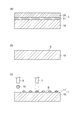
- FIG. 1 is a process diagram showing an embodiment of a method for producing a light guide plate.
- the method which concerns on this embodiment is the process of peeling the protective film 2 which has the adhesion layer 21 provided on the base film 25 and the surface of the resin board 15 provided on the base film 25 from the resin board 15. And forming a dot-shaped pattern by disposing the ink 10 by ink jet printing on the surface S on which the adhesive layer of the resin plate 15 is bonded, and reflecting dots 11 from the ink 10 forming the pattern. It is mainly comprised from the process to form.
- the light guide plate 1 having the resin plate 15 and the reflective dots 11 provided on the resin plate 15 is manufactured.
- the adhesive layer 21 of the protective film 2 contains an ethylene-vinyl acetate copolymer that is an elastomer.
- the ethylene-vinyl acetate copolymer preferably contains 8 to 20% by mass of monomer units derived from vinyl acetate and 80 to 92% by mass of monomer units derived from ethylene.
- the adhesive layer 21 may contain components other than the ethylene-vinyl acetate copolymer.
- the adhesive layer 21 contains a material selected from rosin resin, coumarone indene resin, coumarone resin and indene resin, which improves the wettability with respect to the adherend (resin plate 15).
- the rosin resin is selected from, for example, rosin, polymerized rosin, hydrogenated rosin, rosin-modified product, and glycerin ester or pentaerythritol ester of rosin or hydrogenated rosin. Of these, hydrogenated rosin is preferred.
- the base film 25 is preferably a polyolefin resin film.
- the polyolefin resin film includes, for example, at least one polyolefin resin selected from low density polyethylene, medium density polyethylene, high density polyethylene, linear low density polyolefin, polypropylene, and ethylene-propylene copolymer.
- the base film 25 may be a single layer film or a multilayer film composed of two or more layers.
- the resin plate 15 is a translucent resin sheet.
- the resin plate 15 is preferably a poly (meth) acrylic acid alkyl resin sheet, a polystyrene sheet, or a polycarbonate resin sheet.
- the protective film 2 is peeled from the resin plate 15 to expose the surface S which is one main surface of the resin plate 15 ((b) in FIG. 1).
- the method for peeling off the protective film 2 is not particularly limited.
- the resin plate 15 having the surface S is used for printing the surface S with ink by an ink jet method to form a print pattern. That is, the resin plate 15 is a resin plate for inkjet printing.
- the ink 10 for forming reflective dots is arranged on the surface S on which the adhesive layer 21 has been bonded to form a dot-like pattern.
- the ink 10 is ejected from the inkjet head 5 in the form of droplets.
- the ink 10 may be ink that forms reflective dots by curing or drying, and for example, ultraviolet curable ink, water-based ink, or solvent ink is used. Among these, ultraviolet curable ink and water-based ink are preferable from the viewpoint of easy environmental measures.
- the ultraviolet curable ink is used, the reflective dots 11 made of the cured ink are formed through a process of curing the ink 10 by irradiating the printed ink 10 with ultraviolet rays from the lamp 7.
- water-based ink or solvent ink is used, the ink is dried by a drying device to form reflective dots. Any type of ink may contain fine particles such as pigments, and may be transparent without fine particles, if necessary.
- the protective film 2 in which the adhesive layer 21 contains an ethylene-vinyl acetate copolymer By using the protective film 2 in which the adhesive layer 21 contains an ethylene-vinyl acetate copolymer, partial disturbance of the shape of the reflective dots 11 in the process from printing to curing is suppressed. For example, it is hard to occur that the base part of the mountain-shaped reflective dot 11 spreads and adjacent reflective dots 11 are connected.
- the light guide plate 1 is suitably used as a light guide plate for an edge light type surface light source device constituting a liquid crystal display device, for example.
- the appropriate amount of ink was set to about 40 pL, and the scanning speed of the inkjet head was set to 200 mm / s. Two seconds after ink landing, the ink was cured by irradiating with an ultraviolet ray with an integrated light quantity of 0.5 J / m 2 to form reflective dots, and the light guide plate of the example was obtained.
- a light guide plate of a comparative example was obtained by the same procedure as in the example except that the protective film was replaced with a film having an adhesive layer containing polyethylene (Hitalex ML2230, manufactured by Hitachi Chemical Co., Ltd.).
- the state of the reflective dots of the light guide plate was visually observed, and the state was determined according to the following criteria.
- the evaluation results are shown in Table 1.
- the light guide plate of the example using the resin plate on which the adhesive layer containing the ethylene-vinyl acetate copolymer was bonded As shown in the table, the light guide plate of the example using the resin plate on which the adhesive layer containing the ethylene-vinyl acetate copolymer was bonded, the shape of the reflective dots formed by the inkjet method was polyethylene. Compared with the light guide plate of the comparative example using the resin plate to which the pressure-sensitive adhesive layer was bonded, it was remarkably improved. That is, according to the present invention, it was confirmed that when the reflective dots of the light guide plate are formed by the inkjet method, the disorder of the pattern of the reflective dots can be sufficiently suppressed.
Landscapes
- Physics & Mathematics (AREA)
- Engineering & Computer Science (AREA)
- Manufacturing & Machinery (AREA)
- General Physics & Mathematics (AREA)
- Optics & Photonics (AREA)
- Planar Illumination Modules (AREA)
Abstract
基材フィルムと該基材フィルム上に設けられ樹脂板の表面に貼合されている粘着層とを有し、該粘着層がエチレン-酢酸ビニル共重合体を含んでいる保護フィルムを、樹脂板から剥離する工程と、樹脂板の前記粘着層が貼合されていた表面に、インクジェット印刷によってインクを配置してドット状のパターンを形成する工程と、前記パターンを形成している前記インクから反射ドットを形成させる工程と、を備える、導光板を製造する方法。
Description
本発明は導光板を製造する方法に関する。
液晶表示装置等の透過型画像表示装置は、一般に、バックライトとしての面光源装置を有している。エッジライト型面光源装置は、透光性樹脂板を有する導光板と、透光性樹脂板の端面に光を供給する光源とから構成される。透光性樹脂板の端面から入射した光が、透光性樹脂板の背面側に設けられた反射ドット等の反射手段によって反射し、導光板の出射面から画像表示用の面状の光が供給される。
導光板を製造するために用いられる透明樹脂原板は、その表面を保護するための保護フィルムが貼合された状態で供給されることがある(例えば、特許文献1参照。)。保護フィルムとしては、製造コスト等の観点から、ポリエチレン系のエラストマーを含む粘着層を有するものが広く用いられている。
透光性樹脂板上に反射ドットを形成する方法として、インクジェット印刷法の適用が提案されている。インクジェット法によれば、所望のパターンを構成する反射ドットを簡易に形成できることが期待される。
しかし、インクジェット法によって反射ドットを形成すると、反射ドットの形状が乱れたり、隣り合う反射ドット同士が連結されたりして、反射ドットを設計通りのパターンで形成できない場合があるという問題があった。反射ドットのパターンの乱れが生じると、導光板としての機能が著しく損なわれ得る。
そこで、本発明の目的は、導光板の反射ドットをインクジェット法によって形成する場合において、反射ドットのパターンの乱れを十分に抑制することにある。
本発明者らの知見によれば、粘着層を有する保護フィルムを樹脂板から剥離したときに、粘着層を形成する粘着剤の一部が樹脂板の表面に残り、残った粘着剤に起因して反射ドットのパターンが乱れると考えられる。特に、インクジェット法により反射ドットを形成する場合に、粘着剤に起因するパターンの乱れが生じやすい。本発明者らは、鋭意検討の結果、特定の成分を含む粘着層を有する保護フィルムを用いることにより、反射ドットのパターンの乱れが抑制されることを見出し、本発明の完成に至った。
すなわち、本発明に係る導光板を製造する方法は、基材フィルムと該基材フィルム上に設けられ樹脂板の表面に貼合されている粘着層とを有し、該粘着層がエチレン-酢酸ビニル共重合体を含んでいる保護フィルムを、樹脂板から剥離する工程と、樹脂板の粘着層が貼合されていた表面に、インクジェット印刷によってインクを配置してドット状のパターンを形成する工程と、前記パターンを形成している前記インクから反射ドットを形成させる工程と、を備える。
本発明はまた、上記本発明に係る製造方法により得ることのできる導光板に関する。本発明に係る導光板は、反射ドットのパターンの乱れを十分に抑制しつつ、インクジェット法の利点を生かした簡易且つ高い効率で製造されることができる。
別の側面において、本発明は、基材フィルムと該基材フィルム上に設けられ樹脂板の表面に貼合されている粘着層とを有し、該粘着層がエチレン-酢酸ビニル共重合体を含んでいる保護フィルムを、樹脂板から剥離する工程を含む方法により得ることのできる、インクジェット印刷用樹脂板に関する。
本発明に係る樹脂板によれば、その表面上にインクをドット状にパターン印刷したときに、印刷パターンの乱れを十分に抑制することができる。本発明に係る樹脂板は、導光板を製造するために好適に用いることができる。
本発明によれば、導光板の反射ドットをインクジェット法によって形成する場合において、反射ドットのパターンの乱れを十分に抑制することができる。
以下、本発明の好適な実施形態について詳細に説明する。ただし、本発明は以下の実施形態に限定されるものではない。
図1は、導光板を製造する方法の一実施形態を示す工程図である。本実施形態に係る方法は、基材フィルム25と基材フィルム25上に設けられ樹脂板15の表面に貼合されている粘着層21とを有する保護フィルム2を、樹脂板15から剥離する工程と、樹脂板15の粘着層が貼合されていた表面Sに、インクジェット印刷によってインク10を配置してドット状のパターンを形成する工程と、パターンを形成しているインク10から反射ドット11を形成させる工程とから主として構成される。この方法により、樹脂板15及び樹脂板15上に設けられた反射ドット11を有する導光板1が製造される。
図1の(a)に示されるように、樹脂板15は、その表面に保護フィルム2が貼合された状態で供給される。保護フィルム2の粘着層21は、エラストマーであるエチレン-酢酸ビニル共重合体を含有している。このエチレン-酢酸ビニル共重合体は、好ましくは、酢酸ビニルに由来する単量体単位8~20質量%と、エチレンに由来する単量体単位80~92質量%とを含む。粘着層21は、エチレン-酢酸ビニル共重合体以外の他の成分を含有していてもよい。好ましくは、粘着層21は、ロジン系樹脂、クマロンインデン樹脂、クマロン樹脂及びインデン樹脂から選ばれる、被着体(樹脂板15)に対する濡れ性を向上させる材料を含有する。ロジン系樹脂は、例えば、ロジン、重合ロジン、水添ロジン、ロジン変性物、及び、ロジン又は水添ロジンのグリセリンエステル又はペンタエリスリットエステルから選ばれる。これらのなかでも水添ロジンが好ましい。
基材フィルム25は、好ましくは、ポリオレフィン系樹脂フィルムである。ポリオレフィン系樹脂フィルムは、例えば、低密度ポリエチレン、中密度ポリエチレン、高密度ポリエチレン、直鎖状低密度ポリオレフィン、ポリプロピレン、及びエチレン-プロピレン共重合体から選ばれる少なくとも1種のポリオレフィン系樹脂を含む。基材フィルム25は、単層のフィルムであってもよいし、2層以上から構成される多層のフィルムであってもよい。
樹脂板15は、透光性の樹脂シートである。具体的には、樹脂板15は、ポリ(メタ)アクリル酸アルキル樹脂シート、ポリスチレンシート又はポリカーボネート系樹脂シートであることが好ましい。
保護フィルム2を樹脂板15から剥離して、樹脂板15の一方の主面である表面Sを露出させる(図1の(b))。保護フィルム2を剥離する方法は特に限定されない。表面Sを有する樹脂板15は、表面Sをインクジェット法によりインクで印刷して印刷パターンを形成するために用いられる。すなわち、樹脂板15はインクジェット印刷用樹脂板である。
次いで、図1の(c)に示されるように、粘着層21が貼合されていた表面Sに、反射ドット形成用のインク10が配置されてドット状のパターンが形成される。インク10は、インクジェットヘッド5から液滴状に吐出される。
インク10は、硬化又は乾燥により反射ドットを形成するインクであればよく、例えば、紫外線硬化インク、水性インク又は溶剤インクが用いられる。これらのなかでも、環境対策の容易さなどの観点から、紫外線硬化インク及び水性インクが好ましい。紫外線硬化インクを用いる場合、印刷されたインク10に対してランプ7により紫外線を照射してインク10を硬化する工程を経て、硬化したインクからなる反射ドット11が形成される。水性インク又は溶剤インクを用いる場合、乾燥装置によりインクが乾燥されて、反射ドットが形成される。いずれの種類のインクも、顔料等の微粒子を含んでいてもよいし、必要に応じて、微粒子を含まない透明なものであってもよい。
粘着層21がエチレン-酢酸ビニル共重合体を含んでいる保護フィルム2を用いたことにより、印刷から硬化に至る過程における反射ドット11の形状の部分的な乱れが抑制される。例えば、山型の反射ドット11の裾部が広がって、隣り合う反射ドット11同士が連結されるようなことが生じ難い。
導光板1は、例えば、液晶表示装置を構成するエッジライト型面光源装置用の導光板として好適に用いられる。
以下、実施例を挙げて本発明についてさらに具体的に説明する。ただし、本発明はこれら実施例に限定されるものではない。
導光板の作製
エチレン-酢酸ビニル共重合体を含む粘着層を有する保護フィルム(東レフィルム加工製、トレテック7232)が表面に貼合されたポリメチルメタクリレート樹脂シート(厚さ4mm、サイズ370mm×100mm)を準備した。このアクリル樹脂シート(ポリメチルメタクリレート樹脂シート)から保護フィルムを剥離し、剥離により露出したアクリル樹脂シートの表面を、紫外線硬化インク(40℃における粘度:8.3mPa・s)を用いたインクジェット法により、解像度300dpi、解像度150dpi又は解像度75dpiで印刷した。インクの液適量は約40pLに、インクジェットヘッドの走査速度は200mm/sに設定した。インク着弾から2秒後、積算光量0.5J/m2の紫外線照射によりインクを硬化して、反射ドットを形成させ、実施例の導光板を得た。
エチレン-酢酸ビニル共重合体を含む粘着層を有する保護フィルム(東レフィルム加工製、トレテック7232)が表面に貼合されたポリメチルメタクリレート樹脂シート(厚さ4mm、サイズ370mm×100mm)を準備した。このアクリル樹脂シート(ポリメチルメタクリレート樹脂シート)から保護フィルムを剥離し、剥離により露出したアクリル樹脂シートの表面を、紫外線硬化インク(40℃における粘度:8.3mPa・s)を用いたインクジェット法により、解像度300dpi、解像度150dpi又は解像度75dpiで印刷した。インクの液適量は約40pLに、インクジェットヘッドの走査速度は200mm/sに設定した。インク着弾から2秒後、積算光量0.5J/m2の紫外線照射によりインクを硬化して、反射ドットを形成させ、実施例の導光板を得た。
保護フィルムを、ポリエチレンを含む粘着層を有するフィルム(日立化成工業製、ヒタレックスML2230)に代えた他は実施例と同様の手順により、比較例の導光板を得た。
評価
導光板の反射ドットの状態を目視により観察し、その状態を以下の基準により判定した。評価結果を表1に示す。
A:隣り合う反射ドット同士が連結されることなく、ほぼ円形の底面を有する反射ドットが形成されている。
B:隣り合う反射ドット同士が連結されている、及び/又は、円形から乱れた形状の底面を有する反射ドットが形成されている。
導光板の反射ドットの状態を目視により観察し、その状態を以下の基準により判定した。評価結果を表1に示す。
A:隣り合う反射ドット同士が連結されることなく、ほぼ円形の底面を有する反射ドットが形成されている。
B:隣り合う反射ドット同士が連結されている、及び/又は、円形から乱れた形状の底面を有する反射ドットが形成されている。

表に示されるように、エチレン-酢酸ビニル共重合体を含む粘着層が貼合されていた樹脂板を用いた実施例の導光板は、インクジェット法により形成された反射ドットの形状が、ポリエチレンを含む粘着層が貼合されていた樹脂板を用いた比較例の導光板と比較して顕著に改善された。すなわち、本発明によれば、導光板の反射ドットをインクジェット法によって形成する場合において、反射ドットのパターンの乱れを十分に抑制することができることが確認された。
1…導光板、2…保護フィルム、5…インクジェットヘッド、7…ランプ、10…インク、11…反射ドット、15…樹脂板、21…粘着層、25…基材フィルム、S…粘着層21が貼合されていた表面。
Claims (3)
- 基材フィルムと該基材フィルム上に設けられ樹脂板の表面に貼合されている粘着層とを有し、該粘着層がエチレン-酢酸ビニル共重合体を含んでいる保護フィルムを、前記樹脂板から剥離する工程と、
前記樹脂板の前記粘着層が貼合されていた表面に、インクジェット印刷によってインクを配置してドット状のパターンを形成する工程と、
前記パターンを形成している前記インクから反射ドットを形成させる工程と、
を備える、導光板を製造する方法。 - 請求項1に記載の方法により得ることのできる導光板。
- 基材フィルムと該基材フィルム上に設けられ樹脂板の表面に貼合されている粘着層とを有し、該粘着層がエチレン-酢酸ビニル共重合体を含んでいる保護フィルムを、前記樹脂板から剥離する工程を含む方法により得ることのできる、インクジェット印刷用樹脂板。
Applications Claiming Priority (2)
| Application Number | Priority Date | Filing Date | Title |
|---|---|---|---|
| JP2011020125A JP2012160378A (ja) | 2011-02-01 | 2011-02-01 | 導光板の製造方法 |
| JP2011-020125 | 2011-02-01 |
Publications (1)
| Publication Number | Publication Date |
|---|---|
| WO2012105295A1 true WO2012105295A1 (ja) | 2012-08-09 |
Family
ID=46602516
Family Applications (1)
| Application Number | Title | Priority Date | Filing Date |
|---|---|---|---|
| PCT/JP2012/050632 Ceased WO2012105295A1 (ja) | 2011-02-01 | 2012-01-13 | 導光板を製造する方法 |
Country Status (3)
| Country | Link |
|---|---|
| JP (1) | JP2012160378A (ja) |
| TW (1) | TW201235693A (ja) |
| WO (1) | WO2012105295A1 (ja) |
Cited By (2)
| Publication number | Priority date | Publication date | Assignee | Title |
|---|---|---|---|---|
| CN110737042A (zh) * | 2018-07-20 | 2020-01-31 | 梅姆斯莱克斯 | 显示装置及导光板 |
| CN112666773A (zh) * | 2019-10-16 | 2021-04-16 | 元太科技工业股份有限公司 | 反射式显示器 |
Families Citing this family (1)
| Publication number | Priority date | Publication date | Assignee | Title |
|---|---|---|---|---|
| JP2015049968A (ja) * | 2013-08-30 | 2015-03-16 | 住友化学株式会社 | 導光板 |
Citations (2)
| Publication number | Priority date | Publication date | Assignee | Title |
|---|---|---|---|---|
| JPH05210004A (ja) * | 1991-11-27 | 1993-08-20 | Meitaku Syst:Kk | 成形エッジライトパネル及びその製造方法 |
| JP2010091604A (ja) * | 2008-10-03 | 2010-04-22 | Mitsubishi Rayon Co Ltd | 保護フィルム付き成形体、およびその製造方法 |
-
2011
- 2011-02-01 JP JP2011020125A patent/JP2012160378A/ja active Pending
-
2012
- 2012-01-13 WO PCT/JP2012/050632 patent/WO2012105295A1/ja not_active Ceased
- 2012-01-19 TW TW101102297A patent/TW201235693A/zh unknown
Patent Citations (2)
| Publication number | Priority date | Publication date | Assignee | Title |
|---|---|---|---|---|
| JPH05210004A (ja) * | 1991-11-27 | 1993-08-20 | Meitaku Syst:Kk | 成形エッジライトパネル及びその製造方法 |
| JP2010091604A (ja) * | 2008-10-03 | 2010-04-22 | Mitsubishi Rayon Co Ltd | 保護フィルム付き成形体、およびその製造方法 |
Cited By (2)
| Publication number | Priority date | Publication date | Assignee | Title |
|---|---|---|---|---|
| CN110737042A (zh) * | 2018-07-20 | 2020-01-31 | 梅姆斯莱克斯 | 显示装置及导光板 |
| CN112666773A (zh) * | 2019-10-16 | 2021-04-16 | 元太科技工业股份有限公司 | 反射式显示器 |
Also Published As
| Publication number | Publication date |
|---|---|
| TW201235693A (en) | 2012-09-01 |
| JP2012160378A (ja) | 2012-08-23 |
Similar Documents
| Publication | Publication Date | Title |
|---|---|---|
| CN104025169B (zh) | 显示器装置用装饰膜和保护面板 | |
| CN102069651B (zh) | 导光板及其印刷方法和背光模组 | |
| JP5899145B2 (ja) | インプリント用下層膜形成組成物およびパターン形成方法 | |
| CN103988100B (zh) | 显示体、转印箔及带显示体的物品 | |
| JP3681978B2 (ja) | 光反射板および反射型液晶表示装置 | |
| CN102681043B (zh) | 光学元件及其制造方法、显示装置、信息输入装置、相片 | |
| WO2009157243A1 (ja) | 導光板及び、導光板の製造方法 | |
| JP2017194568A (ja) | 偏光板およびその製造方法、ならびに該偏光板を用いた画像表示装置 | |
| JP7456269B2 (ja) | マイクロledチップ搬送用フィルム及びマイクロledチップの搬送方法 | |
| WO2012111243A1 (ja) | 印刷物の印刷方法及び印刷物 | |
| WO2012105295A1 (ja) | 導光板を製造する方法 | |
| US20130286687A1 (en) | Light guide with a printed film | |
| JP2010089386A (ja) | シート | |
| JP2013101783A (ja) | 導光板の製造方法、導光板、エッジライト型面光源装置及び透過型画像表示装置 | |
| JP2014035493A (ja) | カバーフィルム、カバーフィルムの製造方法及び表示装置 | |
| JP2018521445A (ja) | 積層された抽出フィルムを含む光ガイド | |
| KR102289805B1 (ko) | 가식 부착 적층체, 광학 적층체 및 플렉서블 화상 표시 장치 | |
| JP2009301919A (ja) | 面発光装置用導光板 | |
| JP2010066568A (ja) | 光回折構造体とその製造方法、ステッカー、漉き込み用紙、包装材 | |
| CN114545539A (zh) | 出光部件和其制造方法及包含其的照明单元 | |
| KR20220129628A (ko) | 화상 표시 장치의 제조 방법 | |
| JP6083042B2 (ja) | 遊技板及び遊技板の製造方法 | |
| JP6805458B2 (ja) | 導光板ユニット、これを備えたバックライトユニットおよび液晶表示装置 | |
| JP2015025884A (ja) | 両面印刷ラベル及び両面印刷ラベルの作製方法 | |
| JP2014206754A (ja) | 表示機器、及び、携帯端末 |
Legal Events
| Date | Code | Title | Description |
|---|---|---|---|
| 121 | Ep: the epo has been informed by wipo that ep was designated in this application |
Ref document number: 12742116 Country of ref document: EP Kind code of ref document: A1 |
|
| NENP | Non-entry into the national phase |
Ref country code: DE |
|
| 122 | Ep: pct application non-entry in european phase |
Ref document number: 12742116 Country of ref document: EP Kind code of ref document: A1 |