WO2012105166A1 - コンデンサ内蔵基板およびこの基板を備えるモジュール - Google Patents
コンデンサ内蔵基板およびこの基板を備えるモジュール Download PDFInfo
- Publication number
- WO2012105166A1 WO2012105166A1 PCT/JP2012/000228 JP2012000228W WO2012105166A1 WO 2012105166 A1 WO2012105166 A1 WO 2012105166A1 JP 2012000228 W JP2012000228 W JP 2012000228W WO 2012105166 A1 WO2012105166 A1 WO 2012105166A1
- Authority
- WO
- WIPO (PCT)
- Prior art keywords
- capacitor
- substrate
- built
- electrode
- capacitors
- Prior art date
- Legal status (The legal status is an assumption and is not a legal conclusion. Google has not performed a legal analysis and makes no representation as to the accuracy of the status listed.)
- Ceased
Links
Images

Classifications
-
- H—ELECTRICITY
- H01—ELECTRIC ELEMENTS
- H01G—CAPACITORS; CAPACITORS, RECTIFIERS, DETECTORS, SWITCHING DEVICES, LIGHT-SENSITIVE OR TEMPERATURE-SENSITIVE DEVICES OF THE ELECTROLYTIC TYPE
- H01G4/00—Fixed capacitors; Processes of their manufacture
- H01G4/002—Details
- H01G4/228—Terminals
-
- H—ELECTRICITY
- H01—ELECTRIC ELEMENTS
- H01G—CAPACITORS; CAPACITORS, RECTIFIERS, DETECTORS, SWITCHING DEVICES, LIGHT-SENSITIVE OR TEMPERATURE-SENSITIVE DEVICES OF THE ELECTROLYTIC TYPE
- H01G4/00—Fixed capacitors; Processes of their manufacture
- H01G4/002—Details
- H01G4/005—Electrodes
- H01G4/012—Form of non-self-supporting electrodes
-
- H—ELECTRICITY
- H01—ELECTRIC ELEMENTS
- H01G—CAPACITORS; CAPACITORS, RECTIFIERS, DETECTORS, SWITCHING DEVICES, LIGHT-SENSITIVE OR TEMPERATURE-SENSITIVE DEVICES OF THE ELECTROLYTIC TYPE
- H01G4/00—Fixed capacitors; Processes of their manufacture
- H01G4/002—Details
- H01G4/018—Dielectrics
- H01G4/06—Solid dielectrics
- H01G4/08—Inorganic dielectrics
- H01G4/12—Ceramic dielectrics
-
- H—ELECTRICITY
- H05—ELECTRIC TECHNIQUES NOT OTHERWISE PROVIDED FOR
- H05K—PRINTED CIRCUITS; CASINGS OR CONSTRUCTIONAL DETAILS OF ELECTRIC APPARATUS; MANUFACTURE OF ASSEMBLAGES OF ELECTRICAL COMPONENTS
- H05K1/00—Printed circuits
- H05K1/02—Details
- H05K1/11—Printed elements for providing electric connections to or between printed circuits
- H05K1/115—Via connections; Lands around holes or via connections
-
- H—ELECTRICITY
- H05—ELECTRIC TECHNIQUES NOT OTHERWISE PROVIDED FOR
- H05K—PRINTED CIRCUITS; CASINGS OR CONSTRUCTIONAL DETAILS OF ELECTRIC APPARATUS; MANUFACTURE OF ASSEMBLAGES OF ELECTRICAL COMPONENTS
- H05K1/00—Printed circuits
- H05K1/16—Printed circuits incorporating printed electric components, e.g. printed resistors, capacitors or inductors
- H05K1/162—Printed circuits incorporating printed electric components, e.g. printed resistors, capacitors or inductors incorporating printed capacitors
-
- H—ELECTRICITY
- H05—ELECTRIC TECHNIQUES NOT OTHERWISE PROVIDED FOR
- H05K—PRINTED CIRCUITS; CASINGS OR CONSTRUCTIONAL DETAILS OF ELECTRIC APPARATUS; MANUFACTURE OF ASSEMBLAGES OF ELECTRICAL COMPONENTS
- H05K2201/00—Indexing scheme relating to printed circuits covered by H05K1/00
- H05K2201/09—Shape and layout
- H05K2201/09209—Shape and layout details of conductors
- H05K2201/095—Conductive through-holes or vias
- H05K2201/09545—Plated through-holes or blind vias without lands
-
- H—ELECTRICITY
- H05—ELECTRIC TECHNIQUES NOT OTHERWISE PROVIDED FOR
- H05K—PRINTED CIRCUITS; CASINGS OR CONSTRUCTIONAL DETAILS OF ELECTRIC APPARATUS; MANUFACTURE OF ASSEMBLAGES OF ELECTRICAL COMPONENTS
- H05K3/00—Apparatus or processes for manufacturing printed circuits
- H05K3/40—Forming printed elements for providing electric connections to or between printed circuits
- H05K3/4038—Through-connections; Vertical interconnect access [VIA] connections
- H05K3/4053—Through-connections; Vertical interconnect access [VIA] connections by thick-film techniques
- H05K3/4061—Through-connections; Vertical interconnect access [VIA] connections by thick-film techniques for via connections in inorganic insulating substrates
-
- H—ELECTRICITY
- H05—ELECTRIC TECHNIQUES NOT OTHERWISE PROVIDED FOR
- H05K—PRINTED CIRCUITS; CASINGS OR CONSTRUCTIONAL DETAILS OF ELECTRIC APPARATUS; MANUFACTURE OF ASSEMBLAGES OF ELECTRICAL COMPONENTS
- H05K3/00—Apparatus or processes for manufacturing printed circuits
- H05K3/46—Manufacturing multilayer circuits
- H05K3/4611—Manufacturing multilayer circuits by laminating two or more circuit boards
- H05K3/4626—Manufacturing multilayer circuits by laminating two or more circuit boards characterised by the insulating layers or materials
- H05K3/4629—Manufacturing multilayer circuits by laminating two or more circuit boards characterised by the insulating layers or materials laminating inorganic sheets comprising printed circuits, e.g. green ceramic sheets
Definitions
- the present invention relates to a capacitor built-in substrate that incorporates a capacitor formed by opposing capacitor electrodes and a module including this substrate.
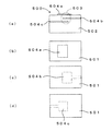
- the capacitor-embedded substrate 500 shown in FIG. 6 includes a stacked body 502 formed by stacking a plurality of dielectric layers 501 and a capacitor 503 provided in the substrate.
- the capacitor 503 includes planar electrodes 504a to 504c (capacitor electrodes) formed by printing using a conductive paste such as Cu or Ag on the surface of each dielectric layer 501 formed of a resin substrate material or ceramic.
- Each dielectric layer 501 is formed by being stacked and facing each other.
- 6A and 6B are diagrams showing an example of a conventional capacitor built-in substrate, where FIG. 6A is a cross-sectional view, and FIGS. 6B to 6D are plan views of dielectric layers forming the capacitor built-in substrate. .
- each of the planar electrodes 504a to 504c is formed on each dielectric layer 501 by printing using a conductive paste, the formed planar electrodes 504a to 504c may be blurred or peeled off from the dielectric layer. There is. Further, in the process of forming the capacitor built-in substrate 500 by laminating the dielectric layers 501 printed with the planar electrodes 504a to 504c, the planar electrodes 504a to 504c may be deformed or damaged. .
- the magnitude of the error in the capacitance of the capacitor 503 due to such bleeding, peeling, or deformation of each of the planar electrodes 504a to 504c is very large compared to the required capacitance of the capacitor 503. It's big and needs improvement.
- the present invention has been made in view of the above-described problems, and an object of the present invention is to provide a capacitor built-in substrate in which a capacitor formed with a small capacity with high accuracy and a module including the substrate are provided.
- the capacitor-embedded substrate of the present invention is a capacitor-embedded substrate including a capacitor formed by opposing capacitor electrodes, and at least one of the capacitor electrodes is formed by filling a via hole with a conductor. It is characterized by being constituted by the end face of the formed via conductor (claim 1).
- the other capacitor electrode may be a planar electrode, and the area of the planar electrode may be larger than the area of the end face of the via conductor forming the one capacitor electrode.
- the other capacitor electrode is constituted by an end face of a via conductor formed by filling a via hole with a conductor, and the area of the end face of the via conductor constituting the other capacitor electrode is the same as that of the one capacitor electrode.
- the area may be larger than the area of the end face of the via conductor to constitute.
- the one capacitor electrode may be formed by end surfaces of the plurality of via conductors that are electrically connected to each other.
- a module of the present invention is characterized by including the capacitor built-in substrate according to any one of claims 1 to 4 (claim 5).
- At least one of the opposing capacitor electrodes forming the capacitor built in the capacitor built-in substrate is constituted by the end face of the via conductor formed by filling the via hole with the conductor.
- the via hole can be accurately formed with a smaller diameter compared to the area of the planar electrode formed by screen printing or the like, the area of the end surface of the via conductor can be formed minutely, Since the electric capacity of the built-in capacitor can be made smaller, it is possible to provide a capacitor built-in substrate that incorporates a capacitor formed with a small capacity with high accuracy.
- the area of the planar electrode constituting the other capacitor electrode is formed larger than the area of the end face of the via conductor constituting one capacitor electrode. For this reason, the end face of the via conductor and the planar electrode always face each other even if a slight displacement occurs in the formation position of the planar electrode and the via conductor when the dielectric layers are laminated. Thereby, it is possible to prevent variation in the capacitance of the capacitor due to the stacking error.
- the area of the end surface of the via conductor which comprises the other capacitor electrode is formed larger than the area of the end surface of the via conductor which comprises one capacitor electrode, Both via conductors always face each other even if a slight misalignment occurs in the conductor formation position. Thereby, it is possible to prevent variation in the capacitance of the capacitor due to the stacking error.
- one capacitor electrode is constituted by end faces of a plurality of via conductors that are electrically connected to each other, a capacitor having a large electric capacity can be formed easily and accurately.
- FIG. 7 is a diagram showing an example of a conventional capacitor built-in substrate, in which (a) is a cross-sectional view, and (b) to (d) are plan views of dielectric layers forming the capacitor built-in substrate.
- FIG. 1 is a cross-sectional view showing an embodiment of the module of the present invention.
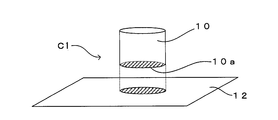
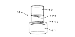
- FIG. 2 and FIG. 3 are enlarged views of main parts showing examples of capacitors built in the capacitor built-in substrate.
- a module 1 shown in FIG. 1 is mounted on a mobile communication terminal such as a mobile phone, and includes a capacitor built-in substrate 2 and ICs, resistors, capacitors, coils, and the like mounted on a component mounting surface of the capacitor built-in substrate 2. It includes various components 3, a mold layer 4 for sealing the component mounting surface, and a plurality of mounting electrodes 5 formed on the back surface of the capacitor-embedded substrate 2, and various components 3 are selected according to the purpose of use.
- Modules with various functions such as Bluetooth (registered trademark) modules, wireless LAN modules, and antenna switch modules for mobile phones (switch ICs, SAW duplexers, etc.) 1 can be formed.
- the capacitor built-in substrate 2 is integrally formed as a dielectric ceramic laminate by laminating and firing a plurality of dielectric layers 21 to 26 formed of ceramic green sheets.
- the ceramic green sheets forming the dielectric layers 21 to 26 are obtained by forming a sheet in which a slurry in which a mixed powder such as alumina and glass is mixed with an organic binder and a solvent is formed by a film forming apparatus. It is formed so that it can be fired at a temperature lower than 0 ° C., so-called low temperature firing.
- the dielectric green layers 21 to 26 are formed on the ceramic green sheet cut into a predetermined shape by forming vias with a laser and printing various patterns with a conductive paste containing Ag, Cu, or the like.
- the dielectric layers 21 to 26 are provided with electrode patterns 13 for electrically connecting various components 3 mounted on the module 1 and mounting electrodes 5 and via conductors 14 for interlayer connection. Further, the end face 10a of the via conductor 10 constituting one capacitor electrode of the capacitor C1 provided on the dielectric layer 23, and the planar electrode 12 constituting the other capacitor electrode of the capacitor C1 provided on the dielectric layer 22; 2 form the capacitor C1 shown in FIG.
- the end face 10a of the via conductor 10 constituting one capacitor electrode of the capacitor C2 provided on the dielectric layer 25 and the via conductor 11 constituting the other capacitor electrode of the capacitor C2 provided on the dielectric layer 23 are also shown.
- the capacitor C3 shown in FIG. 3 is formed by facing the end surface 11a.
- the area of the planar electrode 12 and the end surface 11a of the via conductor 11 is formed larger than the area of the end surface 10a of the via conductor 10 facing each other.
- the via conductors 10 and 11 are formed by filling a via hole formed by laser processing or the like with a conductor paste.
- the mold layer 4 is made of a general mold resin, and the component 3 mounted on the component mounting surface of the capacitor built-in substrate 2 is protected from the external environment by the mold layer 4.
- via holes are formed in a ceramic green sheet formed in a predetermined shape with a laser or the like, and a conductor paste is filled therein, thereby forming via conductors 14 for interlayer connection and via conductors 10 and 11 for forming capacitors C1 and C2.
- the predetermined electrode pattern 13 and the planar electrode 12 are printed with the conductive paste, and ceramic green sheets for forming the dielectric layers 21 to 26 constituting the capacitor built-in substrate 2 are prepared.
- Each ceramic green sheet is provided with a plurality of via conductors 14, via conductors 10 and 11, planar electrodes 12, and electrode patterns 13 so that a large amount of the capacitor built-in substrate 2 can be formed at a time.
- the dielectric layers 21 to 26 are laminated to form a laminated body. And the groove
- the component 3 is mounted on the component mounting surface of the assembly of the capacitor built-in substrate 2 before being divided into individual capacitor built-in substrates 2, and the component mounting of the assembly of the capacitor built-in substrate 2 on which the component 3 is mounted.
- the mold resin is filled in the surface, and this is heated and cured, whereby the mold layer 4 is provided on each capacitor built-in substrate 2, and the assembly of the modules 1 is formed. Then, the assembly of the modules 1 is divided individually, and the module 1 is completed.
- the module 1 including the capacitor built-in substrate 2, the component 3, and the mold layer 4 incorporating the capacitors C1 and C2 is not limited to the above-described manufacturing method, and may be formed by a known general manufacturing method.
- 2 may be formed of a resin multilayer substrate made of glass epoxy resin or the like.
- a coil, a resistor, or the like may be provided in the capacitor built-in substrate 2, and the number of capacitors C1 and C2 incorporated is not limited to the number described above, and is opposed depending on the required electric capacity.
- a capacitor formed by a planar electrode may be built in.
- At least one of the capacitor electrodes constituting the capacitors C1 and C2 built in the capacitor built-in substrate 2 is an end face of the via conductor 10 formed by filling the via hole with the conductive paste. 10a.
- the via hole can be formed with a smaller area and with higher accuracy, and therefore the area of the end face 10a of the via conductor 10 is formed to be very small. be able to.
- the area of the planar electrode 12 constituting the other capacitor electrode of the capacitor C1 is formed larger than the area of the end face 10a of the via conductor 10 constituting one capacitor electrode of the capacitor C1, and each dielectric layer 21
- the end face 10a of the via conductor 10 and the planar electrode 12 always face each other even if a slight misalignment occurs in the positions where the planar electrode 12 and the via conductor 10 are formed. For this reason, it is possible to prevent variation in the electric capacity of the capacitor C1 caused by stacking deviation.
- the area of the end face 11a of the via conductor 11 constituting the other capacitor electrode of the capacitor C2 is formed larger than the area of the end face 10a of the via conductor 10 constituting one capacitor electrode of the capacitor C2.
- the capacitor built-in substrate 2 including the capacitors C1 and C2 that are accurately formed in a minute capacity as described above variation in electrical characteristics is suppressed, and a module 1 having designed characteristics is provided. be able to.
- the processing time required for forming the via conductors 10 and 11 by laser processing is shorter than the processing time required for forming the planar electrode 12 by screen printing. Therefore, the manufacturing time of the module 1 can be shortened by forming the capacitors C1 and C2 built in the capacitor built-in substrate 2 by the via conductors 10a and 11a as described above.
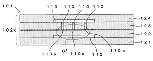
- FIG. 4 is another embodiment of the module of the present invention, and is an enlarged view of a main part showing a capacitor built-in substrate provided in the module.
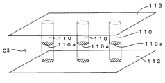
- FIG. 5 is a diagram illustrating an example of a capacitor.
- This embodiment is different from the above-described embodiment in that the capacitor-embedded substrate 102 included in the module 101 shown in FIG. 4 is configured by the end surfaces 110a of the plurality of via conductors 110 that are electrically connected to each other in addition to the capacitors C1 and C2.
- the capacitor C3 formed by facing one capacitor electrode and the other capacitor electrode formed by the planar electrode 112 is built in. Since the other configuration is the same as that of the above-described embodiment, description of the configuration is omitted by assigning a corresponding symbol.
- one capacitor electrode forming the capacitor C ⁇ b> 3 is electrically connected to each other through an electrode pattern 113 provided in the dielectric layer 124, and a plurality of vias provided in the dielectric layer 123. It is constituted by the end face 110a of the conductor 110.
- the other capacitor electrode forming the capacitor C3 is constituted by the planar electrode 112 provided on the dielectric layer 122.
- the planar electrode 112 is formed larger than the total area of the end surfaces 110a of the plurality of via conductors 110.
- the other capacitor electrode constituting the capacitor C3 may be constituted by the end faces 110a of the plurality of via conductors 110 that are electrically connected to each other in the same manner as the one capacitor electrode.
- one capacitor electrode is constituted by the end surfaces 110a of the plurality of via conductors 110 that are electrically connected to each other.
- the capacitors formed by the end faces 110a of the individual via conductors 110 are connected in parallel, so that the capacitor C3 having a relatively large capacitance can be easily formed with high accuracy.
- each of the via conductors 10 and 11 is possible.
- Via conductors 10 and 11 may be formed such that the end surfaces 10a and 11a have the same area.
- the present invention can be widely applied to a capacitor built-in substrate in which a capacitor formed by opposing capacitor electrodes is built.
Landscapes
- Engineering & Computer Science (AREA)
- Power Engineering (AREA)
- Microelectronics & Electronic Packaging (AREA)
- Manufacturing & Machinery (AREA)
- Chemical & Material Sciences (AREA)
- Ceramic Engineering (AREA)
- Inorganic Chemistry (AREA)
- Production Of Multi-Layered Print Wiring Board (AREA)
Abstract
精度よく微小容量に形成されたコンデンサを内蔵するコンデンサ内蔵基板を提供する。 コンデンサ内蔵基板2に内蔵されるコンデンサC1,C2を形成する対向するコンデンサ電極のうち、少なくとも一方は、ビアホールに導体が充填されて形成されたビア導体10の端面10aにより形成されているが、スクリーン印刷などにより形成される平面電極12の面積と比較すると、より小さな直径で精度よくビアホールを形成することによりビア導体10の端面10aの面積を非常に小さく形成することができ、基板2に内蔵されるコンデンサC1,C2の電気容量をより小さなものとすることができるため、精度よく微小容量に形成されたコンデンサC1,C2を内蔵するコンデンサ内蔵基板2を提供することができる。
Description
本発明は、対向するコンデンサ電極により形成されるコンデンサを内蔵するコンデンサ内蔵基板およびこの基板を備えるモジュールに関する。
近年、携帯電話などの携帯端末の小型化に伴い、携帯端末に搭載されるモジュールの小型化を図るために、コンデンサを内蔵するコンデンサ内蔵基板が採用されている(例えば特許文献1参照)。例えば、図6に示すコンデンサ内蔵基板500は、複数の誘電体層501が積層されて形成される積層体502と、基板内に設けられたコンデンサ503とを備えている。そして、コンデンサ503は、樹脂基板材料やセラミックにより形成された各誘電体層501の表面にCuやAgなどの導電体ペーストを用いた印刷により形成された平面電極504a~504c(コンデンサ電極)が、各誘電体層501が積層されて対向することにより形成される。なお、図6は、従来のコンデンサ内蔵基板の一例を示す図であって、(a)は断面図、(b)~(d)はコンデンサ内蔵基板を形成する各誘電体層の平面図である。
ところで、近年、通信容量を拡大するため、携帯電話などの携帯端末のより一層の高周波化が要望されており、コンデンサ内蔵基板500に内蔵されるコンデンサ503の電気容量を微小化することが要求されている。さらに、微小容量のコンデンサ503を内蔵するコンデンサ内蔵基板500の電気的特性が、基板ごとにばらつかないようにするために、各誘電体層501に、平面電極504a~504cの面積を微小に、かつ、精度よく形成する必要性が生じている。
ところが、各平面電極504a~504cは、導電体ペーストを用いた印刷により各誘電体層501に形成されるため、形成された各平面電極504a~504cが滲んだり、誘電体層から剥がれたりするおそれがある。また、平面電極504a~504cが印刷された各誘電体層501が積層されることによりコンデンサ内蔵基板500が形成される過程において、各平面電極504a~504cが変形したりして破損するおそれがある。
このような、各平面電極504a~504cの滲みや剥がれ、変形などに起因する、コンデンサ503の電気容量の誤差の大きさは、要求されているコンデンサ503の電気容量の大きさに対して非常に大きなものであり、改善が求められている。
この発明は、上記した課題に鑑みてなされたものであり、精度よく微小容量に形成されたコンデンサを内蔵するコンデンサ内蔵基板およびこの基板を備えるモジュールを提供することを目的とする。
上記した目的を達成するために、本発明のコンデンサ内蔵基板は、対向するコンデンサ電極により形成されるコンデンサを内蔵するコンデンサ内蔵基板において、前記コンデンサ電極の少なくとも一方は、ビアホールに導体が充填されて形成されたビア導体の端面により構成されていることを特徴としている(請求項1)。
また、他方の前記コンデンサ電極は、平面電極により構成されて、前記平面電極の面積は前記一方のコンデンサ電極を形成するビア導体の端面の面積よりも大きくするとよい(請求項2)。
また、他方の前記コンデンサ電極は、ビアホールに導体が充填されて形成されたビア導体の端面により構成されて、前記他方のコンデンサ電極を構成するビア導体の端面の面積は、前記一方のコンデンサ電極を構成するビア導体の端面の面積よりも大きくしてもよい(請求項3)。
また、前記一方のコンデンサ電極は、互いに導通する複数の前記ビア導体の端面により形成されていてもよい(請求項4)。
また、本発明のモジュールは、請求項1ないし4のいずれかに記載のコンデンサ内蔵基板を備えることを特徴としている(請求項5)。
請求項1の発明によれば、コンデンサ内蔵基板に内蔵されるコンデンサを形成する対向するコンデンサ電極のうち、少なくとも一方は、ビアホールに導体が充填されて形成されたビア導体の端面により構成されている。この場合、スクリーン印刷などにより形成される平面電極の面積と比較すると、ビアホールをより小さな直径で精度よく形成することができるため、ビア導体の端面の面積を微小に形成することができ、基板に内蔵されるコンデンサの電気容量をより小さなものとすることができるため、精度よく微小容量に形成されたコンデンサを内蔵するコンデンサ内蔵基板を提供することができる。
請求項2の発明によれば、他方のコンデンサ電極を構成する平面電極の面積が、一方のコンデンサ電極を構成するビア導体の端面の面積よりも大きく形成されている。このため、各誘電体層を積層する際に平面電極およびビア導体の形成位置に多少の位置ずれが生じても、ビア導体の端面および平面電極は必ず対向する。これにより、積層ずれに起因するコンデンサの電気容量にばらつきが生じるのを防止することができる。
請求項3の発明によれば、他方のコンデンサ電極を構成するビア導体の端面の面積が、一方のコンデンサ電極を構成するビア導体の端面の面積よりも大きく形成されており、一方および他方のビア導体の形成位置に多少の位置ずれが生じても、両ビア導体は必ず対向する。これにより、積層ずれに起因するコンデンサの電気容量にばらつきが生じるのを防止することができる。
請求項4の発明によれば、一方のコンデンサ電極が、互いに導通する複数のビア導体の端面により構成されているため、電気容量の大きなコンデンサを容易に精度よく形成することができる。
請求項5の発明によれば、精度よく微小容量に形成されたコンデンサを内蔵するコンデンサ内蔵基板を備えることにより、電気的特性のばらつきが抑制され、設計通りの特性を有するモジュールを提供することができる。
<一実施形態>
本発明のコンデンサ内蔵基板を備えるモジュールの一実施形態について図1~図3を参照して説明する。図1は本発明のモジュールの一実施形態を示す断面図である。図2および図3はそれぞれコンデンサ内蔵基板に内蔵されるコンデンサの一例を示す要部拡大図である。
本発明のコンデンサ内蔵基板を備えるモジュールの一実施形態について図1~図3を参照して説明する。図1は本発明のモジュールの一実施形態を示す断面図である。図2および図3はそれぞれコンデンサ内蔵基板に内蔵されるコンデンサの一例を示す要部拡大図である。
図1に示すモジュール1は、携帯電話などの携帯通信端末に搭載されるものであり、コンデンサ内蔵基板2と、コンデンサ内蔵基板2の部品実装面に実装されるIC、抵抗、コンデンサ、コイルなどの各種の部品3と、部品実装面を封止するモールド層4と、コンデンサ内蔵基板2の裏面に形成された複数の実装用電極5とを備え、使用目的に応じて種々の部品3が選択されてコンデンサ内蔵基板2の部品実装面に実装されることにより、Bluetooth(登録商標)モジュールや無線LANモジュール、携帯電話用のアンテナスイッチモジュール(スイッチICやSAWデュプレクサなど)など、種々の機能を有するモジュール1を形成することができる。
コンデンサ内蔵基板2は、この実施形態では、セラミックグリーンシートにより形成された複数の誘電体層21~26が積層されて焼成されることで一体的に誘電体セラミック積層体として形成されており、内部にはビア導体10,11および平面電極12により形成されたコンデンサC1,C2が設けられている。各誘電体層21~26を形成するセラミックグリーンシートは、アルミナおよびガラスなどの混合粉末が有機バインダおよび溶剤などと一緒に混合されたスラリーが成膜装置によりシート化されたものであり、約1000℃よりも低い温度で、所謂、低温焼成できるように形成されている。そして、所定形状に切り取られたセラミックグリーンシートに、レーザーによるビア形成、AgやCuなどを含む導体ペーストによる種々のパターン印刷が行われて各誘電体層21~26が形成される。
各誘電体層21~26には、モジュール1に実装される各種部品3および実装用電極5を電気的に接続するための電極パターン13および層間接続用のビア導体14が設けられている。また、誘電体層23に設けられたコンデンサC1の一方のコンデンサ電極を構成するビア導体10の端面10aと、誘電体層22に設けられたコンデンサC1の他方のコンデンサ電極を構成する平面電極12とが対向することで、図2に示すコンデンサC1が形成される。
また、誘電体層25に設けられたコンデンサC2の一方のコンデンサ電極を構成するビア導体10の端面10aと、誘電体層23に設けられたコンデンサC2の他方のコンデンサ電極を構成するビア導体11の端面11aとが対向することで、図3に示すコンデンサC3が形成される。なお、平面電極12およびビア導体11の端面11aの面積は、それぞれに対向するビア導体10の端面10aの面積よりも大きく形成されている。また、ビア導体10,11は、レーザー加工などにより形成されたビアホールに導体ペーストが充填されて形成される。
モールド層4は、一般的なモールド樹脂により形成されており、モールド層4により、コンデンサ内蔵基板2の部品実装面に実装された各部品3は外部環境から保護される。
次に、図1のモジュール1の製造方法の一例についてその概略を説明する。
まず、所定形状に形成されたセラミックグリーンシートに、レーザーなどでビアホールを形成し、内部に導体ペーストを充填することにより層間接続用のビア導体14およびコンデンサC1,C2形成用のビア導体10,11が形成され、導体ペーストにより所定の電極パターン13および平面電極12が印刷されて、コンデンサ内蔵基板2を構成する各誘電体層21~26を形成するためのセラミックグリーンシートが準備される。なお、それぞれのセラミックグリーンシートには、一度に大量のコンデンサ内蔵基板2を形成できるように、ビア導体14、ビア導体10,11、平面電極12、電極パターン13が複数設けられている。
次に、各誘電体層21~26が積層されて積層体が形成される。そして、焼成後に個々のコンデンサ内蔵基板2に分割するための溝が、個々のコンデンサ内蔵基板2の領域を囲むように形成される。続いて、積層体が加圧されながら低温焼成されることによりコンデンサ内蔵基板2の集合体が形成される。
次に、個々のコンデンサ内蔵基板2に分割される前に、コンデンサ内蔵基板2の集合体の部品実装面に部品3が実装され、部品3が実装されたコンデンサ内蔵基板2の集合体の部品実装面にモールド樹脂が充填されて、これが加熱硬化されることによりモールド層4が各コンデンサ内蔵基板2上に設けられて、モジュール1の集合体が形成される。そして、モジュール1の集合体は個々に分割されて、モジュール1が完成する。
なお、コンデンサC1,C2を内蔵するコンデンサ内蔵基板2、部品3、モールド層4を備えるモジュール1は、上記した製造方法に限らず、周知の一般的な製造方法により形成すればよく、コンデンサ内蔵基板2を、ガラスエポキシ樹脂などによる樹脂多層基板などにより形成してもよい。また、コンデンサ内蔵基板2内に、コイルや抵抗などを設けてもよく、内蔵されるコンデンサC1,C2の数は上記した数に限られるものではなく、必要とされる電気容量に応じて、対向する平面電極により形成されたコンデンサを内蔵してもよい。
以上のように、この実施形態では、コンデンサ内蔵基板2に内蔵されるコンデンサC1,C2を構成するコンデンサ電極のうち、少なくとも一方は、ビアホールに導体ペーストが充填されて形成されたビア導体10の端面10aにより形成されている。本実施形態によれば、スクリーン印刷などにより形成される平面電極12と比較すると、より小さな面積で精度よくビアホールを形成することができるため、ビア導体10の端面10aの面積を非常に小さく形成することができる。これにより、精度よく微小容量に形成されたコンデンサC1,C2を内蔵するコンデンサ内蔵基板2を提供することができる。
また、コンデンサC1の他方のコンデンサ電極を構成する平面電極12の面積が、コンデンサC1の一方のコンデンサ電極を構成するビア導体10の端面10aの面積よりも大きく形成されており、各誘電体層21~26が積層される際に、平面電極12およびビア導体10の形成位置に多少の位置ずれが生じても、ビア導体10の端面10aおよび平面電極12は必ず対向する。このため、積層ずれに起因するコンデンサC1の電気容量にばらつきが生じるのを防止することができる。
また、コンデンサC2の他方のコンデンサ電極を構成するビア導体11の端面11aの面積が、コンデンサC2の一方のコンデンサ電極を構成するビア導体10の端面10aの面積よりも大きく形成されており、各誘電体層21~26が積層される際に、ビア導体10,11の形成位置に多少の位置ずれが生じても、両ビア導体10,11は必ず対向する。このため、積層ずれに起因するコンデンサC2の電気容量にばらつきが生じるのを防止することができる。
また、上記したように精度よく微小容量に形成されたコンデンサC1,C2を内蔵するコンデンサ内蔵基板2を備えることにより、電気的特性のばらつきが抑制され、設計通りの特性を有するモジュール1を提供することができる。
また、一般的に、スクリーン印刷により平面電極12を形成するのに必要な処理時間と比較すれば、レーザー加工によりビア導体10,11を形成するのに必要な処理時間の方が短時間で済むため、上記したようにビア導体10a,11aによりコンデンサ内蔵基板2に内蔵されるコンデンサC1,C2を形成することにより、モジュール1の製造時間の短縮を図ることができる。
<他の実施形態>
本発明のコンデンサ内蔵基板を備えるモジュールの他の実施形態について図4および図5を参照して説明する。図4は本発明のモジュールの他の実施形態であって、モジュールが備えるコンデンサ内蔵基板を示す要部拡大図である。図5はコンデンサの一例を示す図である。
本発明のコンデンサ内蔵基板を備えるモジュールの他の実施形態について図4および図5を参照して説明する。図4は本発明のモジュールの他の実施形態であって、モジュールが備えるコンデンサ内蔵基板を示す要部拡大図である。図5はコンデンサの一例を示す図である。
この実施形態が上記した実施形態と異なる点は、図4に示すモジュール101が備えるコンデンサ内蔵基板102が、上記したコンデンサC1,C2の他に、互いに導通する複数のビア導体110の端面110aにより構成された一方のコンデンサ電極と、平面電極112により構成された他方のコンデンサ電極とが対向することにより形成されたコンデンサC3を内蔵する点である。その他の構成は上記した実施形態と同様の構成であるため、相当符号を付すことによりその構成の説明は省略する。
図4および図5に示すように、コンデンサC3を形成する一方のコンデンサ電極は、誘電体層124に設けられた電極パターン113を介して互いに導通し、誘電体層123に設けられた複数のビア導体110の端面110aにより構成される。また、コンデンサC3を形成する他方のコンデンサ電極は、誘電体層122に設けられた平面電極112により構成される。また、平面電極112は、複数のビア導体110の端面110aの総面積よりも大きく形成されている。
なお、コンデンサC3を構成する他方のコンデンサ電極を、一方のコンデンサ電極と同様に、互いに導通する複数のビア導体110の端面110aにより構成してもよい。
以上のように、この実施形態によれば、上記した実施形態と同様の効果を奏することができると共に、一方のコンデンサ電極が、互いに導通する複数のビア導体110の端面110aにより構成されているため、個々のビア導体110の端面110aにより形成される電気容量が並列接続されて、比較的に電気容量の大きなコンデンサC3を容易に精度よく形成することができる。
なお、本発明は上記した実施形態に限定されるものではなく、その趣旨を逸脱しない限りにおいて、上記したもの以外に種々の変更を行なうことが可能であり、例えば、ビア導体10,11のそれぞれの端面10a,11aの面積が、同じ面積となるようにビア導体10,11を形成してもよい。
本発明は、対向するコンデンサ電極により形成されるコンデンサを内蔵するコンデンサ内蔵基板に広く適用することができる。
1,101 モジュール
2,102 コンデンサ内蔵基板
10,11,110 ビア導体
10a,11a,110a 端面
12,112 平面電極
C1,C2,C3 コンデンサ
2,102 コンデンサ内蔵基板
10,11,110 ビア導体
10a,11a,110a 端面
12,112 平面電極
C1,C2,C3 コンデンサ
Claims (5)
- 対向するコンデンサ電極により形成されるコンデンサを内蔵するコンデンサ内蔵基板において、
前記コンデンサ電極の少なくとも一方は、ビアホールに導体が充填されて形成されたビア導体の端面により形成されていることを特徴とするコンデンサ内蔵基板。 - 他方の前記コンデンサ電極は、平面電極により形成されて、前記平面電極の面積は前記一方のコンデンサ電極を形成するビア導体の端面の面積よりも大きいことを特徴とする請求項1に記載のコンデンサ内蔵基板。
- 他方の前記コンデンサ電極は、ビアホールに導体が充填されて形成されたビア導体の端面により形成されて、前記他方のコンデンサ電極を形成するビア導体の端面の面積は、前記一方のコンデンサ電極を形成するビア導体の端面の面積よりも大きいことを特徴とする請求項1に記載のコンデンサ内蔵基板。
- 前記一方のコンデンサ電極は、互いに導通する複数の前記ビア導体の端面により形成されていることを特徴とする請求項1ないし3のいずれかに記載のコンデンサ内蔵基板。
- 請求項1ないし4のいずれかに記載のコンデンサ内蔵基板を備えるモジュール。
Applications Claiming Priority (2)
| Application Number | Priority Date | Filing Date | Title |
|---|---|---|---|
| JP2011018309 | 2011-01-31 | ||
| JP2011-018309 | 2011-01-31 |
Publications (1)
| Publication Number | Publication Date |
|---|---|
| WO2012105166A1 true WO2012105166A1 (ja) | 2012-08-09 |
Family
ID=46602396
Family Applications (1)
| Application Number | Title | Priority Date | Filing Date |
|---|---|---|---|
| PCT/JP2012/000228 Ceased WO2012105166A1 (ja) | 2011-01-31 | 2012-01-17 | コンデンサ内蔵基板およびこの基板を備えるモジュール |
Country Status (1)
| Country | Link |
|---|---|
| WO (1) | WO2012105166A1 (ja) |
Citations (3)
| Publication number | Priority date | Publication date | Assignee | Title |
|---|---|---|---|---|
| JPH1168261A (ja) * | 1997-08-25 | 1999-03-09 | Denso Corp | 配線基板 |
| JP2005311156A (ja) * | 2004-04-23 | 2005-11-04 | Matsushita Electric Ind Co Ltd | コンデンサを内蔵したセラミック多層基板 |
| JP2006261651A (ja) * | 2005-03-18 | 2006-09-28 | Samsung Electro Mech Co Ltd | ブラインドビアホールを備えたキャパシタ内蔵型プリント回路基板およびその製造方法 |
-
2012
- 2012-01-17 WO PCT/JP2012/000228 patent/WO2012105166A1/ja not_active Ceased
Patent Citations (3)
| Publication number | Priority date | Publication date | Assignee | Title |
|---|---|---|---|---|
| JPH1168261A (ja) * | 1997-08-25 | 1999-03-09 | Denso Corp | 配線基板 |
| JP2005311156A (ja) * | 2004-04-23 | 2005-11-04 | Matsushita Electric Ind Co Ltd | コンデンサを内蔵したセラミック多層基板 |
| JP2006261651A (ja) * | 2005-03-18 | 2006-09-28 | Samsung Electro Mech Co Ltd | ブラインドビアホールを備えたキャパシタ内蔵型プリント回路基板およびその製造方法 |
Similar Documents
| Publication | Publication Date | Title |
|---|---|---|
| US9384898B2 (en) | Multilayer ceramic capacitor and method of manufacturing the same | |
| JP5404312B2 (ja) | 電子装置 | |
| US8879234B2 (en) | Laminated ceramic electronic component | |
| KR20130091270A (ko) | 적층 세라믹 전자부품의 제조방법 | |
| KR20140081360A (ko) | 적층 세라믹 커패시터, 그 제조방법 및 적층 세라믹 커패시터가 실장된 회로기판 | |
| KR20120122590A (ko) | 칩형 코일 부품 | |
| JP2014187216A (ja) | 積層セラミックコンデンサの製造方法 | |
| US20130271240A1 (en) | Through-hole via inductor in a high-frequency device | |
| KR20000011521A (ko) | 인덕터소자및그제조방법 | |
| CN115798864B (zh) | 一种片式电感器及其制造方法 | |
| KR20120000529A (ko) | 세라믹 전자 부품 및 그 제조 방법 | |
| US7926154B2 (en) | Method of manufacturing multi-layer ceramic condenser | |
| US10122339B2 (en) | Composite electronic component and board having the same | |
| US8879237B2 (en) | Multilayer ceramic electronic component and method of manufacturing the same | |
| KR102436222B1 (ko) | 기판 내장용 적층 세라믹 전자 부품, 그 제조 방법 및 적층 세라믹 전자 부품 내장형 인쇄회로기판 | |
| JP4821302B2 (ja) | セラミック多層基板及びその製造方法 | |
| KR20090051627A (ko) | 다층 세라믹 기판 및 그의 제조방법 | |
| KR101477426B1 (ko) | 기판 내장용 적층 세라믹 전자부품 및 적층 세라믹 전자부품 내장형 인쇄회로기판 | |
| WO2012105166A1 (ja) | コンデンサ内蔵基板およびこの基板を備えるモジュール | |
| KR100951264B1 (ko) | 적층 세라믹 기판 제조방법 | |
| KR100946017B1 (ko) | 세라믹 기판의 제조 방법 | |
| KR100951265B1 (ko) | 적층 세라믹 기판 제조방법 | |
| KR100916075B1 (ko) | 다층 세라믹기판 제조방법 | |
| JP5838978B2 (ja) | セラミック積層部品 | |
| US12381036B2 (en) | Manufacturing method of capacitor component |
Legal Events
| Date | Code | Title | Description |
|---|---|---|---|
| 121 | Ep: the epo has been informed by wipo that ep was designated in this application |
Ref document number: 12742141 Country of ref document: EP Kind code of ref document: A1 |
|
| NENP | Non-entry into the national phase |
Ref country code: DE |
|
| 122 | Ep: pct application non-entry in european phase |
Ref document number: 12742141 Country of ref document: EP Kind code of ref document: A1 |
|
| NENP | Non-entry into the national phase |
Ref country code: JP |