WO2012105101A1 - 発光素子、光電気混載基板および発光装置 - Google Patents
発光素子、光電気混載基板および発光装置 Download PDFInfo
- Publication number
- WO2012105101A1 WO2012105101A1 PCT/JP2011/076102 JP2011076102W WO2012105101A1 WO 2012105101 A1 WO2012105101 A1 WO 2012105101A1 JP 2011076102 W JP2011076102 W JP 2011076102W WO 2012105101 A1 WO2012105101 A1 WO 2012105101A1
- Authority
- WO
- WIPO (PCT)
- Prior art keywords
- electrode
- light
- dielectric layer
- emitting element
- light emitting
- Prior art date
- Legal status (The legal status is an assumption and is not a legal conclusion. Google has not performed a legal analysis and makes no representation as to the accuracy of the status listed.)
- Ceased
Links
Images




Classifications
-
- H—ELECTRICITY
- H05—ELECTRIC TECHNIQUES NOT OTHERWISE PROVIDED FOR
- H05B—ELECTRIC HEATING; ELECTRIC LIGHT SOURCES NOT OTHERWISE PROVIDED FOR; CIRCUIT ARRANGEMENTS FOR ELECTRIC LIGHT SOURCES, IN GENERAL
- H05B33/00—Electroluminescent light sources
- H05B33/10—Apparatus or processes specially adapted to the manufacture of electroluminescent light sources
-
- H—ELECTRICITY
- H05—ELECTRIC TECHNIQUES NOT OTHERWISE PROVIDED FOR
- H05B—ELECTRIC HEATING; ELECTRIC LIGHT SOURCES NOT OTHERWISE PROVIDED FOR; CIRCUIT ARRANGEMENTS FOR ELECTRIC LIGHT SOURCES, IN GENERAL
- H05B33/00—Electroluminescent light sources
- H05B33/12—Light sources with substantially two-dimensional [2D] radiating surfaces
- H05B33/26—Light sources with substantially two-dimensional [2D] radiating surfaces characterised by the composition or arrangement of the conductive material used as an electrode
Definitions
- the present invention relates to a light emitting element, an opto-electric hybrid board, and a light emitting device.
- An inorganic electroluminescence (EL) element is expected to be used as a new display element that does not require a separate light source as a self-light-emitting light source.
- EL electroluminescence
- inorganic EL elements are realized using inorganic compounds (for example, see Patent Document 1 and Non-Patent Document 1).
- a conventional dispersion-type EL element an AC voltage is applied to an element having phosphor particles (for example, ZnS: Cu, Cl) whose current path is blocked between electrodes, whereby the phosphor particles emit electroluminescence.
- the optimum particle size of the phosphor particles is considered to be about 10 ⁇ m, and it is known that the emission luminance is remarkably lowered when the particle size is smaller than 2 to 3 ⁇ m.
- This dispersion type EL element is considered to emit light by recombination between a donor and an acceptor.
- the conventional thin-film EL element has an alternating current with an element having a phosphor light-emitting layer (for example, ZnS: Mn doped with Mn as a light emission center in a base material ZnS) sandwiched between insulating electrodes between electrodes.
- a phosphor light-emitting layer for example, ZnS: Mn doped with Mn as a light emission center in a base material ZnS
- CMOS circuits which are information processing devices and memory devices, are realized based on semiconductors centering on silicon, if light emitting elements can be created simultaneously with other functional elements such as transistors on a substrate such as silicon, The information processing device, the memory device, and the light-emitting element can be manufactured over the same substrate. This is expected to enable inter-chip communication and optical computing technology using light, and lead to further development of digital electronic devices.
- an electroluminescence having a peak of about 650 nm by forming a nanometer order cluster (emission center) of silicon in a silicon nitride film (insulator) on a silicon substrate and applying a voltage to the silicon nitride film.
- a nanometer order cluster emission center
- silicon nitride film insulator
- a high voltage of about 100 V is applied to the electrodes on both sides of the insulator film, and a strong electric field of about 7 MV / cm is applied to the insulator film. is required.
- the electrons of the electrode are supplied to the conduction band of the insulator film by FN (Fowler-Nordheim) tunneling, and after the electrons are accelerated by the electric field to obtain sufficient kinetic energy, the emission center is excited to emit light. It has been.
- FN Fluler-Nordheim
- light emission from conventional light-emitting elements in which a light emission center is formed in an insulator film is in the visible light region, most of which is light in a region with a relatively long wavelength such as red, and has a luminance, area, and light emission that can withstand practical use. Such uniformity is not actually realized. From the viewpoint of realization of individual lighting that replaces a display or a fluorescent lamp, a light emitting element that emits light with high brightness and uniformity in a shorter wavelength region is desired.
- a light-emitting element that can be directly fabricated on a semiconductor substrate and can be selectively fabricated in a very small region which has been the biggest problem in the construction of optical circuits in recent years, is desired.
- the present invention has been made in view of such circumstances, and can be easily manufactured on a semiconductor substrate, and emits light with higher luminance particularly in a short wavelength region of blue to green (about 450 to 550 nm).
- a light emitting device is provided.
- the present invention includes a first electrode made of a semiconductor containing impurities, a translucent second electrode, and a dielectric layer sandwiched between the first and second electrodes, and the first electrode is ion-implanted
- a light emitting device comprising an atom, wherein the atom has a concentration peak in the first electrode within 500 nm from the interface between the dielectric layer and the first electrode.
- a first electrode made of a semiconductor containing impurities, a translucent second electrode, and a dielectric layer sandwiched between the first and second electrodes are provided, and the first electrode is ion-implanted. Therefore, the emission center can be formed by the ion-implanted atoms. For this reason, by applying a voltage between the first electrode and the second electrode, the emission center can emit light, and light can be extracted through the translucent second electrode.
- the present invention since it includes the first electrode, the second electrode, and the dielectric layer, it can be directly formed on a semiconductor substrate such as a silicon substrate, and is selectively manufactured in a very small region. be able to. Further, unlike conventional EL elements and LEDs, it can be easily built into a silicon semiconductor circuit without using a multi-component material or a very multilayer structure.
- the light-emitting element of the present invention includes a first electrode made of a semiconductor containing an impurity, a translucent second electrode, and a dielectric layer sandwiched between the first and second electrodes. It has an implanted atom, and the atom has a concentration peak in the first electrode within 500 nm from the interface between the dielectric layer and the first electrode.
- the first electrode and the dielectric layer have ion-implanted atoms.
- the ion implantation step can be performed after the dielectric layer is formed on the first electrode.
- an emission center can be formed both in the first electrode and in the dielectric layer.
- the total amount of ion-implanted atoms in the first electrode is preferably larger than the total amount of ion-implanted atoms in the dielectric layer. According to such a configuration, the light emission intensity of the light emitting element can be increased.
- the ion-implanted atoms in the first electrode are preferably Ge atoms or Si atoms. According to such a configuration, the light emitting element can emit light. In the light-emitting device of the present invention, it is preferable that the ion-implanted atoms in the first electrode form a light-emitting center composed of clusters, unpaired electrons or ions of 1 nm or less. According to such a configuration, a voltage can be applied to the light emitting element to cause the light emission center to emit light.
- the first electrode is preferably a silicon substrate or a part thereof, and the dielectric layer is preferably made of SiO 2 , SiN or SiON. According to such a configuration, the dielectric layer can be formed by a normal semiconductor manufacturing process.
- the first electrode is preferably made of an n-type semiconductor. According to such a configuration, the light emitting element can emit light better.
- the dielectric layer preferably has a thickness of 5 nm to 75 nm. According to such a configuration, a voltage applied to the light emitting element can be reduced, and power consumption accompanying light emission can be reduced.
- the ion-implanted atoms in the first electrode are implanted with an ion implantation amount of 1 ⁇ 10 15 ion / cm 2 or more and 1 ⁇ 10 17 ion / cm 2 or less. According to such a configuration, a light emission center can be formed in the light emitting element.
- the first electrode preferably has an impurity concentration of 1 ⁇ 10 14 / cm 3 or more and less than 1 ⁇ 10 17 / cm 3 . According to such a configuration, the light emission intensity of the light emitting element can be increased.
- the first electrode preferably has a resistivity of 0.05 ⁇ ⁇ cm to 8 ⁇ ⁇ cm. According to such a configuration, the light emission intensity of the light emitting element can be increased.
- the light emitting device of the present invention further includes a semiconductor substrate, the first electrode is a part of the semiconductor substrate, and the dielectric layer and the second electrode are 0.1 ⁇ m 2 or more and 0.1 mm 2 or less of the semiconductor. It is preferably provided on the area of the substrate. According to such a configuration, a light emitting element can be mounted on a semiconductor substrate on which an electronic circuit is formed, and optical communication between a plurality of electronic circuits is possible.
- the light emitting device of the present invention preferably further comprises a photocatalyst portion provided on the opposite side of the second electrode to the dielectric layer side. According to such a configuration, light emitted by applying a voltage between the first electrode and the second electrode can be emitted to the photocatalyst portion, and the photocatalyst portion can have photocatalytic activity.
- the present invention is a circuit in which the light-emitting element and the semiconductor circuit of the present invention are provided on a semiconductor substrate, the semiconductor circuit is electrically connected to the light-emitting element and performs signal processing.
- the light-emitting element also provides an opto-electric hybrid board that optically outputs a signal that has been processed by the semiconductor circuit. According to the opto-electric hybrid board of the present invention, it is possible to optically output a signal that has been subjected to arithmetic processing by a semiconductor circuit, and optical communication between a plurality of semiconductor circuits becomes possible.
- the present invention includes the light emitting device of the present invention and a power supply circuit for applying a voltage between the first electrode and the second electrode, and the power supply circuit has a current having a constant direction and the dielectric.
- a light emitting device electrically connected to the light emitting element so as to flow through the layer is also provided. According to the light emitting device of the present invention, the light emitting element of the present invention can emit light while suppressing heat generation.
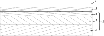
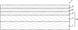
- FIGS. 1, 3, and 4 are cross-sectional views showing the structure of the light-emitting element of this embodiment.
- FIG. 2 is a graph showing the concentration distribution of ion-implanted atoms included in the light emitting device of this embodiment.
- the light emitting element 7 of the present embodiment includes a first electrode 1 made of a semiconductor containing impurities, a translucent second electrode 6, and a dielectric layer 3 sandwiched between the first electrode 1 and the second electrode 6.
- the first electrode 1 contains ion-implanted atoms, and the atoms ion-implanted into the first electrode 1 are within the first electrode 1 within 500 nm from the interface between the dielectric layer 3 and the first electrode 1. It has a concentration peak inside.
- the light emitting element 7 of the present embodiment may further include a photocatalyst unit 8.
- the light-emitting element 7 of the present embodiment will be described.
- the first electrode 1 is made of an n-type semiconductor or a p-type semiconductor.
- the 1st electrode 1 contains the impurity used as a donor
- the 1st electrode 1 consists of a p-type semiconductor
- it contains the impurity used as an acceptor.
- the first electrode 1 when the first electrode 1 is made of crystalline silicon or amorphous silicon and is an n-type semiconductor, the first electrode 1 contains impurities such as P, As, and Sb as a donor.
- the first electrode 1 is made of crystalline silicon or amorphous silicon and is a p-type semiconductor, the first electrode 1 contains impurities such as B and Al as an acceptor.
- the concentration of impurities contained in the first electrode 1 is not particularly limited, but may be, for example, 1 ⁇ 10 14 / cm 3 or more and less than 1 ⁇ 10 17 / cm 3 . Thereby, the light emission intensity of the light emitting element 7 can be further increased.
- the electrical resistivity of the first electrode 1 that varies depending on the impurity concentration in the first electrode 1 can be, for example, 0.05 ⁇ ⁇ cm or more and 8 ⁇ ⁇ cm or less. Thereby, the light emission intensity of the light emitting element 7 can be further increased.
- the form of the 1st electrode 1 is not specifically limited, For example, a semiconductor substrate may be sufficient, a part of semiconductor substrate may be sufficient, and the semiconductor layer formed on the substrate may be sufficient.
- a thermal oxide film of the semiconductor substrate can be used for the dielectric layer 3.
- the dielectric layer 3 can be a SiO 2 film which is a thermal oxide film thereof.
- the light emitting element 7 can be formed on an area of 0.1 ⁇ m 2 or more and 0.1 mm 2 or less of the semiconductor substrate. Thereby, the light emitting element 7 can be mounted on the opto-electric hybrid board described later, and optical communication can be facilitated between electronic circuits.
- the first electrode 1 has ions implanted. This will be described later.
- the first electrode 1 may have a light emission center formed by ion-implanted atoms.
- the first electrode 1 may be formed by diffusing an n-type impurity or a p-type impurity in a semiconductor substrate, or may be formed by forming a semiconductor film on the substrate by a CVD method or the like.
- the dielectric layer 3 is formed on the first electrode 1.
- the dielectric layer 3 is made of an insulator such as silicon oxide, silicon nitride, or silicon oxynitride.
- a strong electric field of about 7 MV / cm can be applied between the first electrode 1 and the second electrode 6, which contributes to the light emission of the light emitting element 7 to the dielectric layer 3. Electrons having kinetic energy can flow.
- the dielectric layer 3 has a large electrical resistivity, it is possible to reduce the flow of electrons having a small kinetic energy that does not contribute to light emission, and to improve effective light emission efficiency. 7 can emit light with low power consumption.
- the dielectric material layer 3 has translucency. As a result, light emitted by applying a voltage between the first electrode 1 and the second electrode 6 can be efficiently extracted through the dielectric layer 3.
- the light transmittance of light having a wavelength of 250 nm or more and 500 nm or less of the dielectric layer 3 is preferably 50% or more. As a result, the light extraction efficiency can be further increased.
- silicon oxide, silicon nitride, or silicon oxynitride is used for the dielectric layer 3, these materials are relatively difficult to transmit oxygen, so that they are formed by atoms implanted into the first electrode 1 or the dielectric layer 3. It is possible to suppress oxidation of the emitted light centers.
- the light emitting element 7 can emit light stably.
- silicon oxide, particularly thermal silicon oxide showed particularly good characteristics. This is presumably because the thermal silicon oxide film has the fewest defects, so that the electrons from the second electrode 6 are rarely trapped in the middle, or a leak path is formed and no voltage is applied.
- the thickness of the dielectric layer 3 is not particularly limited, but may be 5 nm or more and 100 nm or less. In this case, the voltage applied between the first electrode 1 and the second electrode 6 when the light emitting element 7 emits light can be further reduced. Further, the thickness of the dielectric layer 3 may be a range between any two of 5, 10, 20, 25, 30, 35, 40, 50, 60, 70, 75, 80, 90 and 100 nm. Good. The thickness of the dielectric layer 3 is particularly preferably 5 nm or more and 75 nm or less. As a result, the voltage applied between the first electrode 1 and the second electrode 6 can be further reduced, and electrons having a large kinetic energy contributing to the light emission of the light-emitting element 7 can be applied to the dielectric layer 3.
- the thickness of the dielectric layer 3 was less than 5 nm, only a large amount of current flowed experimentally, and almost no light emission could be confirmed visually.
- the thickness of the dielectric layer 3 exceeds 75 nm, the voltage at which light emission becomes strong approaches 100 V, and when it exceeds 100 nm, the voltage at which light emission starts exceeds 100 V, which is not practical.
- the dielectric layer 3 can be formed by thermally oxidizing the semiconductor substrate to form a thermal oxide film, and by CVD or the like on the semiconductor substrate.
- the dielectric layer 3 can also be formed.
- the dielectric layer 3 can be a thermal oxide film made of SiO 2 formed by thermally oxidizing the silicon substrate.
- a silicon oxide film, a silicon nitride film, or a silicon oxynitride film can be formed. Since these dielectric layers 3 can be formed by a normal silicon semiconductor process, the light emitting element 7 is excellent in mass productivity and can be combined with other electronic circuits.
- the dielectric layer 3 may have ion-implanted atoms. This will be described later.
- the dielectric layer 3 may have a light emission center formed by ion-implanted atoms.
- the first electrode 1 has ion implanted atoms.
- the dielectric layer 3 can also have ion implanted atoms.
- the ion-implanted atoms are not particularly limited as long as a light emission center can be formed, and are, for example, Ge atoms, Si atoms, C atoms, or O atoms. In particular, Ge atom is preferable. Since the first electrode 1 or the dielectric layer 3 has ions implanted therein, a light emission center can be formed in the first electrode 1 or the dielectric layer 3, and the first electrode 1 and the second electrode 6 can be formed. The light emission center can be made to emit light by applying a voltage between them.
- the emission center Although details of the emission center are unknown, it is considered to be a cluster, unpaired electron or ion of 1 nm or less. It is considered that the light emitting element 7 emits light when the light emission center is excited by electrons accelerated by the electric field between the first electrode 1 and the second electrode 6.
- the ion-implanted atoms contained in the light emitting element 7 have a concentration peak in the first electrode 1 within 500 nm from the interface between the dielectric layer 3 and the first electrode 1. Thereby, the light emission intensity of the light emitting element can be increased.
- the reason for this is not clear, but is considered as follows.
- the presence of the dielectric layer 3 between the second electrode 6 and the first electrode 1 generates a sufficient electric field, and electrons are sufficiently accelerated toward the second electrode 6 and the first electrode 1 so that sufficient energy is obtained. Is considered to win. Electrons that have acquired this energy can enter the first electrode 1, and the emission center in the first electrode 1 can be excited.
- the first electrode 1 is made of a semiconductor, it is considered that electrons that have lost the energy after the excitation of the emission center and electrons that have not contributed to the excitation of the emission center are quickly discharged from the first electrode 1 without staying. It is done. If the electrons stay, charge-up occurs, and electrons from the second electrode 6 are not sufficiently accelerated, cannot reach the emission center, or cannot obtain sufficient energy, thereby exciting the emission center. It may not be possible to emit enough light. For example, if the concentration peak of atoms contributing to light emission is in the dielectric 3, typically the emission center is in the dielectric 3, electrons that have lost energy by exciting the emission center will pass through the dielectric 3.
- the concentration peak of the ion-implanted atom is the portion of the first electrode 1 where the concentration of the ion-implanted atom is the highest.
- the concentration peak of the ion-implanted atoms has, for example, an interface between the dielectric layer 3 and the first electrode 1 or a depth from this interface of 1, 5, 10, 15, 20, 30, 50, 100, It may be in the first electrode 1 of 200, 400, 500 nm, or may be in the range between any two of these numbers.
- the concentration distribution of the ion-implanted atoms can be expressed by simulation based on conditions for ion implantation into the dielectric layer 3 or the first electrode 1.
- the ion-implanted atoms may be directly ion-implanted into the first electrode 1, or after the dielectric layer 3 is formed on the first electrode 1, the ions may be implanted from above the dielectric layer 3. .
- the ion-implanted atoms have, for example, a concentration distribution as shown by the solid line in FIG.
- the implanted ions have a concentration distribution as shown by a one-dot chain line in FIG. 2.
- the ion implantation amount of the atoms implanted into the first electrode 1 or the dielectric layer 3 is, for example, 1 ⁇ 10 15 , 2 ⁇ 10 15 , 5 ⁇ 10 15 , 10 ⁇ 10 15 , 20 ⁇ 10 15 , 50 ⁇ 10. 15 or 100 ⁇ 10 15 ions / cm 2 , or a range between any two of these numbers.
- the ion acceleration energy at the time of ion implantation into the first electrode 1 or the dielectric layer 3 is, for example, 5, 10, 15, 20, 30, 50, 100, 200, 400 keV, or any of these numerical values. Or a range between two numbers.
- the atoms ion-implanted in the first electrode 1 or the dielectric layer 3 may form fine particles.
- heat treatment is performed in an inert gas atmosphere or an atmosphere containing oxygen, whereby the implanted ions can be aggregated to form fine particles. it can.
- the fine particles may be partially oxidized.
- fine particles partially oxidized can be formed by heat-treating the ion-implanted atoms in an atmosphere containing oxygen. By aggregating the ion-implanted atoms by heat treatment in an atmosphere containing oxygen, smaller particles can be obtained.
- the heat treatment can be performed in an atmospheric gas containing oxygen of 5% to 25%.
- fine particles partially oxidized may be obtained by aggregating the ion-implanted atoms in an inert gas atmosphere and then performing heat treatment in an atmosphere containing oxygen.
- Ge atoms Ge ions
- the first electrode 1 and the dielectric layer 3 are heat-treated to thereby form Ge in the first electrode 1 and the dielectric layer 3.
- Fine particles containing atoms can be formed.
- fine particles containing a zero-valent Ge atom, a divalent Ge atom (GeO), and a tetravalent Ge atom (GeO 2 ) can be formed.
- the first electrode 1 emits light even when it is made of a p-type semiconductor, but emits light more stably when it is made of an n-type semiconductor. The reason for this is not clear, but when the first electrode 1 is made of a p-type semiconductor, the positive charge of majority carriers is attracted to the silicon substrate near the dielectric layer 3 when a voltage is applied, and the second electrode 6 to the first electrode 1 It is conceivable that the electrons coming toward the hinder the excitation of the emission center. When the first electrode is made of an n-type semiconductor, electrons of majority carriers are discharged from the silicon substrate near the dielectric layer 3 so that electrons coming from the second electrode 6 toward the first electrode 1 are present on the silicon substrate.
- the first electrode 1 may be an intrinsic semiconductor, but in that case, the resistance of the first electrode 1 increases, and it is considered that the light emission efficiency is lowered because excess electrons are not efficiently discharged. On the contrary, when the first electrode 1 is made of a semiconductor and the impurity concentration for forming the n-type or p-type is high, the resistance of the first electrode 1 is lowered and the efficiency of discharging excess electrons is improved. It is considered that there are cases where electrons coming from the second electrode 6 toward the first electrode 1 inhibit the excitation of the emission center due to the presence of many impurities or many majority carriers.
- the first electrode 1 when a semiconductor is used for the first electrode 1, the first electrode 1 is thinned leaving only a portion where many emission centers exist, and aluminum is formed on the side opposite to the dielectric 3 side of the first electrode 1. It is considered that by further providing a low-resistance conductive material such as the above, it is possible to achieve both the efficiency of exciting the luminescent center and the efficiency of discharging excess electrons, thereby increasing the luminous efficiency.
- the thickness of the first electrode 1 can be set to be not less than 1 and not more than 3 times the depth of the concentration peak of atoms implanted into the first electrode 1.
- the thickness of the first electrode 1 can be about twice the depth of the concentration peak of the atoms ion-implanted into the first electrode 1. This is because it is thick enough to contain most of the implanted atoms. If importance is attached to the efficiency of discharging and discharging excess electrons, the thickness of the first electrode 1 can be set to the depth of the concentration peak of the ion-implanted atoms. Therefore, when this method is adopted, the thickness of the first electrode 1 is preferably 100 nm or more and 1000 nm or less.
- the second electrode 6 has translucency and is provided on the dielectric layer 3.
- the second electrode 6 is one electrode for applying a voltage to the dielectric layer 3.
- the second electrode 6 can transmit light emitted from the light emitting element 7.
- the second electrode 6 may be a light-transmitting electrode itself or a gap serving as a light path.
- the second electrode 6 having translucency in itself is, for example, a metal oxide thin film such as ITO, a metal thin film such as Al, Ti, or Ta, or a semiconductor thin film such as Si, SiC, or GaN. These can be formed by, for example, sputtering or CVD.
- the second electrode 6 may have a light transmittance of 50% or more and 99.99% or less within a wavelength range of 250 to 500 nm.
- the second electrode 6 having a gap serving as an optical path is, for example, a conductor having a perforated structure such as a slit structure or a porous structure.
- a conductor having a perforated structure such as a slit structure or a porous structure.
- a voltage can be applied to the dielectric layer 3 at the conductor portion, and light that has passed through the gap between the conductors can be extracted.
- the second electrode 6 having a perforated structure can be produced using, for example, conductive nanowires.
- the nanowires for example, silicon, preferably a silicon nanowire doped with doping to increase conductivity, a carbon nanotube, or a metal nanorod can be used.
- the photocatalyst part 8 is provided on the opposite side of the second electrode 6 to the dielectric layer 3 side, and can receive light emitted by applying a voltage between the first electrode 1 and the second electrode 6. .
- the photocatalyst portion 8 can be provided as shown in FIGS.
- the photocatalyst portion 8 can be a photocatalyst thin film.
- a portion near the surface of the photocatalytic portion 8 having photocatalytic activity can receive light, and the photocatalytic portion 8 can have high photocatalytic activity.
- the dirt adhering to the photocatalyst unit 8 can be removed, and the gas or liquid brought into contact with the photocatalyst unit 8 can be purified.
- the photocatalyst portion 8 can be made of titanium oxide TiO 2 which is a photocatalyst. This is because titanium oxide is generally easily available and has photocatalytic activity with excitation light having a wavelength of 388 nm. When titanium oxide is irradiated with light having energy greater than or equal to the band gap, electrons are excited from the valence band to the conduction band, electrons are generated in the conduction band and holes are generated in the valence band, and are photoexcited. Titanium oxide has a characteristic that the band gap is 3.2 eV, recombination of electrons and holes hardly occurs, and the deactivation rate due to recombination is small. Titanium oxide uses anatase type rather than rutile type.
- the band gap of the anatase type is 3.23 eV, which is larger than the rutile type 3.02 eV, the energy of electrons and holes generated by light absorption is large, and recombination of electrons and holes is less likely. is there.
- the photocatalyst unit 8 includes platinum (Pt), palladium (Pd), ruthenium (Ru), rhodium (Rh), gold (Au), silver (Ag), copper (Cu), iron (Fe), nickel (Ni ), Zinc (Zn), gallium (Ga), germanium (Ge), indium (In), and tin (Sn), and may be titanium oxide on which at least one metal is supported. This is because the inclusion of a small amount of the above metals can be expected to increase the excitation wavelength band and improve the generation efficiency of electrons and holes.
- an insulating layer 10 may be provided between the photocatalyst unit 8 and the second electrode 6.
- the second electrode 6 and the photocatalyst portion 8 can be electrically insulated. Thereby, it is possible to prevent the potential of the second electrode 6 from affecting the photocatalytic activity of the photocatalytic portion 8.
- the insulating layer 10 can have a light transmitting property. As a result, the photocatalyst unit 8 can receive light.
- the insulating layer 10 is not particularly limited as long as it is an insulating layer, and is, for example, silicon oxide, silicon nitride, or silicon oxynitride.
- the insulating layer 10 can be formed by depositing silicon oxide, silicon nitride, or the like on the second electrode 6 by CVD or sputtering, for example.
- Diagram 5 of the opto-electric hybrid board is a schematic plan view showing the structure of the opto-electric hybrid board of the present embodiment
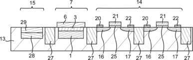
- FIG. 6 is a schematic sectional view showing the structure of the opto-electric hybrid board of the present embodiment.
- the light emitting element 7 and the semiconductor circuit 14 are provided on the semiconductor substrate 13.
- the semiconductor circuit 14 is electrically connected to the light emitting element 7 and performs signal processing.
- the light-emitting element 7 is a circuit, and is characterized by optically outputting a signal that has been subjected to arithmetic processing by the semiconductor circuit 14.
- the opto-electric hybrid board 30 may include the light receiving element 15.
- the semiconductor substrate 13 is not particularly limited as long as it is a semiconductor substrate on which the light emitting element 7 and the semiconductor circuit 14 can be provided.
- a silicon substrate, a germanium substrate, a silicon compound substrate, or a germanium compound substrate. is there.
- the semiconductor substrate 13 may be an impurity semiconductor substrate to which an n-type impurity or a p-type impurity is added.
- the semiconductor substrate 13 may be made by forming a silicon layer and a germanium layer on the SiO 2 or the like substrate, an insulating layer such as SiO 2 is formed on such a Si substrate, a silicon layer and a germanium layer on its May be formed.
- the light emitting element 7 may be formed on a crystalline silicon substrate, or on an insulator layer such as SiO 2 by using a CVD method or the like. Amorphous silicon may be formed, and the light emitting element 7 may be formed thereon. This is because conventional semiconductor circuits such as CMOS circuits are manufactured on a substrate made of a group IV element material.
- the semiconductor circuit 14 is not particularly limited as long as it is a circuit that is provided on the semiconductor substrate 13 and is electrically connected to the light emitting element 7 and performs signal processing.
- the semiconductor circuit 14 is a semiconductor circuit composed of a plurality of transistors and the like.
- it is a semiconductor integrated circuit.
- the semiconductor circuit 14 may be a part other than the light emitting element 7 of the semiconductor integrated circuit.
- the light-emitting element 7 is an element that is provided on the semiconductor substrate 13 and includes the first electrode 1, the second electrode 6, and the dielectric layer 3 sandwiched between the first electrode 1 and the second electrode 6.
- the light emitting element 7 outputs the signal that the semiconductor circuit 14 has performed the arithmetic processing.
- the electrical signal calculated by the semiconductor circuit 14 can be converted into an optical signal by the light emitting element 7 and output.
- the light emitting element 7 can emit light by applying a voltage between the first electrode 1 and the second electrode 6.
- a plurality of the light emitting elements 7 may be provided on the semiconductor substrate 13.
- One or more of the light emitting elements 7 are formed by forming a phosphor-containing layer on the second electrode 6, thereby converting the light emission wavelength. 7 may be sufficient.
- An encoding circuit can also be provided between the light emitting element 7 and the semiconductor circuit 14. As a result, the light emitting element 7 can optically output the signal that the semiconductor circuit 14 has performed arithmetic processing. Note that the encoding circuit may be included in the semiconductor circuit 14.
- the light receiving element 15 may be provided on the semiconductor substrate 13.
- the light receiving element 15 is electrically connected to the semiconductor circuit 14 and can receive light output from other light emitting elements.
- an optical signal input from the outside by the light receiving element 15 can be converted into an electrical signal, and the semiconductor circuit 14 can process the signal input by the light receiving element 15. Therefore, since the opto-electric hybrid board 30 includes the light-emitting element 7 and the light-receiving element 15, high-speed optical communication can be performed between the plurality of opto-electric hybrid boards.
- a decoder circuit may be provided between the light receiving element 15 and the semiconductor circuit 14. As a result, the encoded signal received by the light receiving element 15 can be decoded and transmitted to the semiconductor circuit 14.
- the light receiving element 15 has a region in which an n-type region 28 and a p-type region 29 are pn-junctioned.
- the semiconductor substrate 13 is a p-type semiconductor or an n-type semiconductor, one of the p-type region 29 and the n-type region 28 can be omitted.
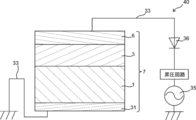
- FIG. 7 is a schematic sectional view of the light emitting device of the present embodiment
- FIG. 8 is a schematic circuit diagram of the light emitting device of the present embodiment.
- the light-emitting device 40 of this embodiment includes a light-emitting element 7 and a power supply circuit 33 for applying a voltage between the first electrode 1 and the second electrode 6. Is electrically connected to the light emitting element 7 so as to flow through the dielectric layer 3.
- the electric energy of the voltage applied between the first electrode 1 and the second electrode 6 can be efficiently converted into light energy. That is, when the first electrode 1 is the positive electrode and the second electrode 6 is the negative electrode and a current is passed through the dielectric layer 3, and when the first electrode 1 is the negative electrode and the second electrode 6 is the positive electrode and the current is passed through the dielectric layer 3 In one of the cases, when light emission is larger, a current in this direction can be passed through the dielectric layer 3. As a result, it is possible to prevent the electrical energy of the voltage applied between the first electrode 1 and the second electrode 6 from being converted into thermal energy and the like, and to reduce the light emission efficiency. Heat generation can be suppressed.
- the power supply circuit 33 is an electric circuit for applying power supplied from the drive power supply 35 to the light emitting element 7.
- the power supply circuit 33 applies a voltage between the first electrode 1 and the second electrode 6 so that a current having a constant direction flows through the dielectric layer 3.
- the power output from the drive power supply 35 is supplied to the light emitting element 7 by the power supply circuit 33.
- the driving power source 35 may be a DC power source or an AC power source as long as the direction of the current flowing through the dielectric layer 3 is constant.
- the drive power supply 35 may include a rectifier diode 36 in the power supply circuit 33 for applying a voltage to the dielectric layer 3. This makes it possible to convert the power supply having the opposite polarity and output a desired polarity voltage.
- the drive power supply 35 may include a booster circuit or a step-down circuit in the power supply circuit 33 for applying a voltage to the dielectric layer 3.
- the output of the drive power supply 35 can be converted into a desired voltage value and output to the light emitting element 7.
- the “current having a constant direction” means a current having a constant direction in which the current value increases as the applied voltage increases.
- the drive power supply 35 When the drive power supply 35 is an AC power supply, the drive power supply 35 may be a power supply that outputs a voltage having a desired waveform.
- the drive power supply 35 may output, for example, a rectangular wave voltage or a sine wave voltage.
- FIGS. 8A to 8C are circuit diagrams showing various power supply circuits 33 that output a voltage to the light emitting element 7 by the drive power supply 35.
- the drive power supply 35 is, for example, a low-voltage sine wave AC power supply as shown in FIG. 8A, and a booster circuit and a rectifier diode 36 are provided between the light-emitting element 7 and electrically connected to the light-emitting element 7. Good.
- the voltage output from the drive power supply 35 can be converted into a desired voltage value by the booster circuit, and only a half wave can be output to the light emitting element 7 by the rectifier diode 36.
- a current having a constant direction of current flow can be passed through the light emitting element 7.
- the drive power supply 35 may be an AC power supply as shown in FIG. 8B, for example, and may be electrically connected to the light emitting element 7 by providing a step-down circuit and a rectifier diode 36 between the light emitting element 7.
- the voltage output from the drive power supply 35 can be converted into a desired voltage value by the booster circuit, and only a half wave can be output to the light emitting element 7 by the rectifier diode 36.
- the drive power supply 35 may be a direct current power supply as shown in FIG. 8C, for example, and a DC-DC conversion circuit may be provided between the light emitting element 7 and electrically connected to the light emitting element 7.
- the voltage output from the drive power supply 35 can be converted into a desired voltage value and output to the light emitting element 7 by the DC-DC conversion circuit.
- Light emitting device fabrication experiment 1 A light emitting element manufacturing experiment was conducted by the following method. An n-type silicon substrate having a resistivity of 3-8 ⁇ ⁇ cm (impurity concentration of about 1 ⁇ 10 15 / cm 3 ) and having an about 1.5 cm square is first heat-treated in an oxygen atmosphere at 1000 ° C. for 40 minutes. A SiO 2 film as a dielectric layer was formed on the surface of the silicon substrate. This SiO 2 film has a thickness of about 50 nm. The first electrode is an n-type silicon substrate. Next, Ge ions were implanted into the SiO 2 film with an acceleration energy of 220 keV. The ion implantation amount was 1.6 ⁇ 10 16 ions / cm 2 . FIG.
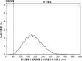
- FIG. 9 shows simulation results of the concentration distribution of ion-implanted Ge atoms in the dielectric layer and the first electrode.
- the ion-implanted Ge atoms have a concentration peak in the first electrode having a depth of about 170 nm from the interface between the second electrode and the dielectric layer.
- an ITO electrode as a second electrode was formed on the SiO 2 film using a sputtering apparatus, an aluminum electrode was formed on the silicon substrate side, and a light emitting element was manufactured.
- a direct current power source was connected to the light emitting element so that the aluminum electrode became a positive electrode and the ITO electrode became a negative electrode, and a voltage was applied to the light emitting element to cause the light emitting element to emit light.
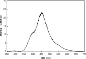
- the emission spectrum is shown in FIG. Referring to FIG. 10, light having a peak at a wavelength of about 450 nm was confirmed with light in a wavelength range of about 340 nm to about 650 nm.
- the wavelength range having an emission intensity at half or more of the emission intensity at the peak of the emission was about 400 nm to about 500 nm. Further, it was confirmed that when a voltage was applied to the light emitting element, light was emitted uniformly over the entire surface of the ITO electrode.
- a heat treatment process can be further added between the ion implantation process and the second electrode formation process.
- the silicon substrate subjected to the above ion implantation was put into an electric furnace, and 50 ml of nitrogen was introduced while being drawn with a rotary pump, and heat treatment was performed at 700 ° C. for 1 hour.
- 10 ml of a gas containing 80% nitrogen and 20% oxygen was introduced, and heat treatment was performed for 1 hour.
- the light emission characteristics were stabilized. The reason for this is not clear, but implantation defects generated in the SiO 2 film as the dielectric layer or the silicon substrate as the first electrode during ion implantation are recovered by heat treatment or formed in the first electrode.
- the emission center is stabilized by approaching a thermal equilibrium state through a heat treatment step. Oxidizing the Ge atoms having entered the dangling bonds and the SiO 2 film of Si-based generated in the SiO 2 film, is prevented to become a charge trap sites contemplated or by performing heat treatment in an oxygen-containing gas .
- Light emitting device fabrication experiment 2 Similar to “Light-Emitting Element Fabrication Experiment 1” using an n-type silicon substrate having a resistivity of 0.01-0.05 ⁇ ⁇ cm (impurity concentration of about 1 ⁇ 10 17 / cm 3 ) and about 1.5 cm square.
- a light emitting element was manufactured by the method described above. A direct current power source was connected to the light emitting element so that the aluminum electrode became a positive electrode and the ITO electrode became a negative electrode, and a voltage was applied to the light emitting element to cause the light emitting element to emit light. However, it was confirmed that this light-emitting element emits light with lower light emission intensity than the light-emitting element manufactured in “Light-emitting element manufacturing experiment 1”.
- Light emitting device fabrication experiment 3 A light emitting element manufacturing experiment was conducted by the following method. Ge ions were implanted at an acceleration energy of 200 keV into an n-type silicon substrate having a resistivity of 3-8 ⁇ ⁇ cm and about 1.5 cm square. The ion implantation amount was 1.0 ⁇ 10 16 ions / cm 2 . Next, a 50 nm SiO 2 film was deposited on the ion-implanted surface of the silicon substrate using plasma CVD. Next, the silicon substrate was put into an electric furnace, and 50 ml of nitrogen was introduced while pulling with a rotary pump, and heat treatment was performed at 700 ° C. for 1 hour.
Landscapes
- Engineering & Computer Science (AREA)
- Manufacturing & Machinery (AREA)
- Electroluminescent Light Sources (AREA)
Abstract
本発明は、半導体基板上に容易に作製することができ、特に青色~緑色(450~550nm程度)の短波長領域でより大きい輝度で発光する発光素子を提供する。本発明の発光素子は、不純物を含む半導体からなる第1電極と、透光性の第2電極と、第1および第2電極に挟まれた誘電体層とを備え、第1電極は、イオン注入された原子を含有し、前記原子は、前記誘電体層と第1電極との界面から500nm以内の第1電極中に濃度ピークを有することを特徴とする。
Description
本発明は、発光素子、光電気混載基板および発光装置に関する。
無機エレクトロルミネッセンス(EL)素子は、自己発光する光源として、別途の光源が不要な新たな表示素子等としての利用が期待されている。
従来のEL素子には、「分散型」と「薄膜型」の2つのタイプが存在し、その多くが交流駆動によって、発光する。
従来のEL素子には、「分散型」と「薄膜型」の2つのタイプが存在し、その多くが交流駆動によって、発光する。
従来の分散型と薄膜型のEL素子については、無機EL素子が無機化合物を用いて実現されている(例えば、特許文献1や非特許文献1参照)。
従来の分散型EL素子は、電極間に電流経路が遮断された蛍光体粒子(例えば、ZnS:Cu,Clなど)を有する素子に交流電圧を印加することにより、蛍光体粒子が電界発光をする。この蛍光体粒子の粒子径は10μm程度が最適であると考えられ、2~3μmよりも小さくなると発光輝度が著しく低下することが知られている。なお、この分散型EL素子は、ドナー・アクセプタ間の再結合により発光すると考えられている。
従来の分散型EL素子は、電極間に電流経路が遮断された蛍光体粒子(例えば、ZnS:Cu,Clなど)を有する素子に交流電圧を印加することにより、蛍光体粒子が電界発光をする。この蛍光体粒子の粒子径は10μm程度が最適であると考えられ、2~3μmよりも小さくなると発光輝度が著しく低下することが知られている。なお、この分散型EL素子は、ドナー・アクセプタ間の再結合により発光すると考えられている。
また、従来の薄膜型EL素子は、電極間に絶縁層で挟まれた蛍光体の発光層(例えば、発光中心となるMnを母材ZnS中にドープしたZnS:Mnなど)を有する素子に交流電圧を印加することにより、発光層が電界発光する。なお、この薄膜型EL素子は、母材中を走るホットエレクトロンによる発光中心の衝突励起により発光すると考えられている。
その一方で、半導体基板、特にシリコン基板上に発光素子を作製する技術の開発が盛んに行われている。情報処理装置や記憶装置であるCMOS回路などはシリコンを中心として半導体を基幹として実現されているため、シリコン等の基板上にトランジスタ等の他の機能素子と同時に発光素子を作成することができれば、情報処理装置や記憶装置と発光素子を同一基板上に作製することができる。このことにより、光によるチップ間通信や光コンピューティング技術が可能となり、更なるデジタル電子機器の発展につながることが期待されている。
例えば、シリコン基板上のシリコン窒化膜(絶縁体)中にシリコンのナノメートルオーダーのクラスター(発光中心)を形成し、このシリコン窒化膜に電圧を印加することによって約650nmのピークを有するエレクトロルミネセンスが確認されたことが知られている(例えば、特許文献2参照)。
なお、従来の絶縁体膜中に発光中心を形成した発光素子は、絶縁体膜の両側の電極に100V程度の高い電圧を印加し、絶縁体膜に7MV/cm程度の強い電界を印加することが必要である。このことにより、電極の電子が絶縁体膜の伝導帯にFN(ファウラー・ノルドハイム)トンネリングによって供給され、この電子が電界により加速され十分な運動エネルギーを得た後、発光中心を励起し発光すると考えられている。
これら従来無機ELのなかには、460~480nm程度の青色を発光する材料も存在するが100V程度かそれ以上の高電圧が必要な上に、充分な輝度が得られていない。
これら従来無機ELのなかには、460~480nm程度の青色を発光する材料も存在するが100V程度かそれ以上の高電圧が必要な上に、充分な輝度が得られていない。
最新無機EL開発動向~材料特性と製造技術・応用展開~、第1版、情報機構、2007年3月27日
しかし、従来の絶縁体膜中に発光中心を形成した発光素子の発光は可視光領域であり、そのほとんどは赤色など波長の比較的長い領域の発光であり、また実用に耐える輝度、面積、発光の均一性等は実際には実現されていない。ディスプレイや、蛍光灯にかわる個体照明の実現等の観点から、より短波長領域で、大きい輝度、むらなく発光する発光素子が望まれている。また、近年光回路を構成する上で最大の課題となっている、半導体基板上に直接作り込みが可能であって極めて微小領域に選択的に作製可能な発光素子が望まれている。
本発明は、このような事情に鑑みてなされたものであり、半導体基板上に容易に作製することができ、特に青色~緑色(450~550nm程度)の短波長領域でより大きい輝度で発光する発光素子を提供する。
本発明は、このような事情に鑑みてなされたものであり、半導体基板上に容易に作製することができ、特に青色~緑色(450~550nm程度)の短波長領域でより大きい輝度で発光する発光素子を提供する。
本発明は、不純物を含む半導体からなる第1電極と、透光性の第2電極と、第1および第2電極に挟まれた誘電体層とを備え、第1電極は、イオン注入された原子を含有し、前記原子は、前記誘電体層と第1電極との界面から500nm以内の第1電極中に濃度ピークを有することを特徴とする発光素子を提供する。
本発明によれば、不純物を含む半導体からなる第1電極と、透光性の第2電極と、第1および第2電極に挟まれた誘電体層とを備え、第1電極は、イオン注入された原子を含有するため、イオン注入された原子により発光中心を形成することができる。このため、第1電極と第2電極との間に電圧を印加することにより、この発光中心を発光させることができ、透光性の第2電極を介して光を取り出すことができる。
本発明によれば、第1電極と第2電極と誘電体層とにより構成されるため、シリコン基板などの半導体基板上に直接作り込むことが可能であり、極めて微少領域に選択的に作製することができる。また、従来のEL素子やLEDとは異なり、多元系の材料や非常に多層な構造を用いることなく容易にシリコン半導体回路に作り込むことができる。
本発明によれば、第1電極と第2電極と誘電体層とにより構成されるため、シリコン基板などの半導体基板上に直接作り込むことが可能であり、極めて微少領域に選択的に作製することができる。また、従来のEL素子やLEDとは異なり、多元系の材料や非常に多層な構造を用いることなく容易にシリコン半導体回路に作り込むことができる。
本発明の発光素子は、不純物を含む半導体からなる第1電極と、透光性の第2電極と、第1および第2電極に挟まれた誘電体層とを備え、第1電極は、イオン注入された原子を有し、前記原子は、前記誘電体層と第1電極との界面から500nm以内の第1電極中に濃度ピークを有することを特徴とする。
本発明の発光素子において、第1電極および前記誘電体層は、イオン注入された原子を有することが好ましい。
このような構成によれば、第1電極の上に誘電体層を形成した後イオン注入工程を行うことができる。また、第1電極中および誘電体層中の両方に発光中心を形成することができる。
本発明の発光素子において、第1電極中のイオン注入された原子の総量は、前記誘電体層中のイオン注入された原子の総量よりも多いことが好ましい。
このような構成によれば、発光素子の発光強度を大きくすることができる。
このような構成によれば、第1電極の上に誘電体層を形成した後イオン注入工程を行うことができる。また、第1電極中および誘電体層中の両方に発光中心を形成することができる。
本発明の発光素子において、第1電極中のイオン注入された原子の総量は、前記誘電体層中のイオン注入された原子の総量よりも多いことが好ましい。
このような構成によれば、発光素子の発光強度を大きくすることができる。
本発明の発光素子において、第1電極中のイオン注入された原子は、Ge原子またはSi原子であることが好ましい。
このような構成によれば、発光素子を発光させることができる。
本発明の発光素子において、第1電極中のイオン注入された原子は、1nm以下のクラスター、不対電子またはイオンからなる発光中心を形成することが好ましい。
このような構成によれば、発光素子に電圧を印加し発光中心を発光させることができる。
このような構成によれば、発光素子を発光させることができる。
本発明の発光素子において、第1電極中のイオン注入された原子は、1nm以下のクラスター、不対電子またはイオンからなる発光中心を形成することが好ましい。
このような構成によれば、発光素子に電圧を印加し発光中心を発光させることができる。
本発明の発光素子において、第1電極は、シリコン基板またはその一部であり、前記誘電体層は、SiO2、SiNまたはSiONからなることが好ましい。
このような構成によれば、誘電体層を通常の半導体製造プロセスにより形成することができる。
本発明の発光素子において、第1電極は、n型半導体からなることが好ましい。
このような構成によれば、発光素子をより良く発光させることができる。
このような構成によれば、誘電体層を通常の半導体製造プロセスにより形成することができる。
本発明の発光素子において、第1電極は、n型半導体からなることが好ましい。
このような構成によれば、発光素子をより良く発光させることができる。
本発明の発光素子において、前記誘電体層は、5nm以上75nm以下の厚さを有することが好ましい。
このような構成によれば、発光素子に印加する電圧を小さくすることができ、発光に伴う消費電力を小さくすることができる。
本発明の発光素子において、第1電極中のイオン注入された原子は、1×10¹⁵ion/cm2以上1×1017ion/cm2以下のイオン注入量で注入されたことが好ましい。
このような構成によれば、発光素子に発光中心を形成することができる。
このような構成によれば、発光素子に印加する電圧を小さくすることができ、発光に伴う消費電力を小さくすることができる。
本発明の発光素子において、第1電極中のイオン注入された原子は、1×10¹⁵ion/cm2以上1×1017ion/cm2以下のイオン注入量で注入されたことが好ましい。
このような構成によれば、発光素子に発光中心を形成することができる。
本発明の発光素子において、第1電極は、1×10¹⁴/cm3以上1×1017/cm3より少ない不純物濃度を有することが好ましい。
このような構成によれば、発光素子の発光強度を大きくすることができる。
本発明の発光素子において、第1電極は、0.05Ω・cm以上8Ω・cm以下の抵抗率を有することが好ましい。
このような構成によれば、発光素子の発光強度を大きくすることができる。
このような構成によれば、発光素子の発光強度を大きくすることができる。
本発明の発光素子において、第1電極は、0.05Ω・cm以上8Ω・cm以下の抵抗率を有することが好ましい。
このような構成によれば、発光素子の発光強度を大きくすることができる。
本発明の発光素子において、半導体基板をさらに備え、第1電極は、前記半導体基板の一部であり、前記誘電体層および第2電極は、0.1μm2以上0.1mm2以下の前記半導体基板の区域上に設けられたことが好ましい。
このような構成によれば、電子回路を形成する半導体基板に発光素子を搭載することができ、複数の電子回路間での光通信が可能となる。
本発明の発光素子において、第2電極の前記誘電体層側の反対側に設けられた光触媒部をさらに備えることが好ましい。
このような構成によれば、第1電極と第2電極との間に電圧を印加することよる発光を光触媒部に照射することができ、光触媒部が光触媒活性を有することができる。
このような構成によれば、電子回路を形成する半導体基板に発光素子を搭載することができ、複数の電子回路間での光通信が可能となる。
本発明の発光素子において、第2電極の前記誘電体層側の反対側に設けられた光触媒部をさらに備えることが好ましい。
このような構成によれば、第1電極と第2電極との間に電圧を印加することよる発光を光触媒部に照射することができ、光触媒部が光触媒活性を有することができる。
また、本発明は、本発明の発光素子と半導体回路とが半導体基板に設けられ、前記半導体回路は、前記発光素子と電気的に接続し、かつ、信号の演算処理を行う回路であり、前記発光素子は、前記半導体回路が演算処理を行った信号を光出力する光電気混載基板も提供する。
本発明の光電気混載基板によれば、半導体回路が演算処理を行った信号を光出力することができ、複数の半導体回路間での光通信が可能となる。
さらに、本発明は、本発明の発光素子と、第1電極と第2電極との間に電圧を印加するための電源回路とを備え、前記電源回路は、向きが一定の電流が前記誘電体層を流れるように前記発光素子と電気的に接続する発光装置も提供する。
本発明の発光装置によれば、発熱することを抑えて本発明の発光素子を発光させることができる。
本発明の光電気混載基板によれば、半導体回路が演算処理を行った信号を光出力することができ、複数の半導体回路間での光通信が可能となる。
さらに、本発明は、本発明の発光素子と、第1電極と第2電極との間に電圧を印加するための電源回路とを備え、前記電源回路は、向きが一定の電流が前記誘電体層を流れるように前記発光素子と電気的に接続する発光装置も提供する。
本発明の発光装置によれば、発熱することを抑えて本発明の発光素子を発光させることができる。
以下、本発明の一実施形態を図面を用いて説明する。図面や以下の記述中で示す構成は、例示であって、本発明の範囲は、図面や以下の記述中で示すものに限定されない。
発光素子の構成
図1、3、4は本実施形態の発光素子の構造を示す断面図である。また、図2は、本実施形態の発光素子に含まれるイオン注入した原子の濃度分布を示すグラフである。
本実施形態の発光素子7は、不純物を含む半導体からなる第1電極1と、透光性の第2電極6と、第1電極1と第2電極6とに挟まれた誘電体層3とを備え、第1電極1は、イオン注入された原子を含有し、第1電極1にイオン注入された原子は、誘電体層3と第1電極1との界面から500nm以内の第1電極1中に濃度ピークを有することを特徴とする。
また、本実施形態の発光素子7は、光触媒部8をさらに有してもよい。
以下、本実施形態の発光素子7について説明する。
図1、3、4は本実施形態の発光素子の構造を示す断面図である。また、図2は、本実施形態の発光素子に含まれるイオン注入した原子の濃度分布を示すグラフである。
本実施形態の発光素子7は、不純物を含む半導体からなる第1電極1と、透光性の第2電極6と、第1電極1と第2電極6とに挟まれた誘電体層3とを備え、第1電極1は、イオン注入された原子を含有し、第1電極1にイオン注入された原子は、誘電体層3と第1電極1との界面から500nm以内の第1電極1中に濃度ピークを有することを特徴とする。
また、本実施形態の発光素子7は、光触媒部8をさらに有してもよい。
以下、本実施形態の発光素子7について説明する。
1.第1電極
第1電極1は、n型半導体またはp型半導体からなる。第1電極1がn型半導体からなる場合、第1電極1はドナーとなる不純物を含み、第1電極1がp型半導体からなる場合、アクセプタとなる不純物を含む。例えば、第1電極1が結晶シリコンまたはアモルファスシリコンからなり、n型半導体である場合、第1電極1は、ドナーとしてP、As、Sbなどの不純物を含む。また、第1電極1が、結晶シリコンまたはアモルファスシリコンからなり、p型半導体である場合、第1電極1は、アクセプタとしてB、Alなどの不純物を含む。
第1電極1は、n型半導体またはp型半導体からなる。第1電極1がn型半導体からなる場合、第1電極1はドナーとなる不純物を含み、第1電極1がp型半導体からなる場合、アクセプタとなる不純物を含む。例えば、第1電極1が結晶シリコンまたはアモルファスシリコンからなり、n型半導体である場合、第1電極1は、ドナーとしてP、As、Sbなどの不純物を含む。また、第1電極1が、結晶シリコンまたはアモルファスシリコンからなり、p型半導体である場合、第1電極1は、アクセプタとしてB、Alなどの不純物を含む。
第1電極1に含まれる不純物濃度は、特に限定されないが、例えば、1×10¹⁴/cm3以上であり1×1017/cm3より小さい濃度とすることができる。このことにより、発光素子7の発光強度をより大きくすることができる。また、第1電極1中の不純物濃度により変化する第1電極1の電気抵抗率は、例えば、0.05Ω・cm以上8Ω・cm以下とすることができる。このことにより、発光素子7の発光強度をより大きくすることができる。
第1電極1の形態は、特に限定されないが、例えば、半導体基板であってもよく、半導体基板の一部であってもよく、基板上に形成された半導体層であってもよい。第1電極1を半導体基板または半導体基板の一部とすることにより、誘電体層3に半導体基板の熱酸化膜を用いることができる。例えば、第1電極1がシリコン基板またはその一部である場合、誘電体層3はその熱酸化膜であるSiO2膜とすることができる。
また、第1電極1を半導体基板の一部とすることにより、半導体基板の0.1μm2以上0.1mm2以下の区域上に発光素子7を形成することができる。このことにより、後述する光電気混載基板に発光素子7を搭載することができ、電子回路間で光通信を容易にすることができる。
また、第1電極1を半導体基板の一部とすることにより、半導体基板の0.1μm2以上0.1mm2以下の区域上に発光素子7を形成することができる。このことにより、後述する光電気混載基板に発光素子7を搭載することができ、電子回路間で光通信を容易にすることができる。
また、第1電極1は、イオン注入された原子を有する。このことは、後述する。また、第1電極1はイオン注入された原子により形成された発光中心を有してもよい。
第1電極1は、半導体基板にn型不純物またはp型不純物を拡散させることにより形成してもよく、基板上にCVD法などにより半導体膜を成膜することにより形成してもよい。
第1電極1は、半導体基板にn型不純物またはp型不純物を拡散させることにより形成してもよく、基板上にCVD法などにより半導体膜を成膜することにより形成してもよい。
2.誘電体層
誘電体層3は、第1電極1上に形成される。誘電体層3は、例えば、酸化シリコン、窒化シリコン又は酸窒化シリコンなどの絶縁体からなる。誘電体層3を設けることにより、第1電極1と第2電極6との間に7MV/cm程度の強い電界を印加することができ、誘電体層3に発光素子7の発光に寄与する大きい運動エネルギーを有する電子を流すことができる。また、誘電体層3は、大きい電気抵抗率を有するため、発光に寄与しない小さい運動エネルギーを有する電子が流れることを低減することができ、実効的な発光効率を向上することができ、発光素子7を低消費電力で発光させることができる。
誘電体層3は、第1電極1上に形成される。誘電体層3は、例えば、酸化シリコン、窒化シリコン又は酸窒化シリコンなどの絶縁体からなる。誘電体層3を設けることにより、第1電極1と第2電極6との間に7MV/cm程度の強い電界を印加することができ、誘電体層3に発光素子7の発光に寄与する大きい運動エネルギーを有する電子を流すことができる。また、誘電体層3は、大きい電気抵抗率を有するため、発光に寄与しない小さい運動エネルギーを有する電子が流れることを低減することができ、実効的な発光効率を向上することができ、発光素子7を低消費電力で発光させることができる。
また、誘電体層3は、透光性を有することが好ましい。このことにより第1電極1と第2電極6との間に電圧を印加することによる発光を誘電体層3を介して効率よく取り出すことができる。誘電体層3の250nm以上500nm以下の波長の光の光透過率は、50%以上であることが好ましい。このことにより、光取り出し効率をより高くすることができる。
また、誘電体層3に酸化シリコン、窒化シリコン又は酸窒化シリコンを用いると、これらの材料は、比較的酸素を透過させにくいため、第1電極1または誘電体層3にイオン注入した原子により形成される発光中心が酸化されることを抑制することができる。このことにより、発光素子7を安定して発光させることができる。
この中でも酸化シリコン、特に熱酸化シリコンは特に良い特性を示した。これは熱酸化シリコン膜がもっとも欠陥が少ないために、第2電極6からの電子が途中でトラップされたり、リークパスができて電圧がかからなくなったりすることが少ないためと考えられる。
また、誘電体層3に酸化シリコン、窒化シリコン又は酸窒化シリコンを用いると、これらの材料は、比較的酸素を透過させにくいため、第1電極1または誘電体層3にイオン注入した原子により形成される発光中心が酸化されることを抑制することができる。このことにより、発光素子7を安定して発光させることができる。
この中でも酸化シリコン、特に熱酸化シリコンは特に良い特性を示した。これは熱酸化シリコン膜がもっとも欠陥が少ないために、第2電極6からの電子が途中でトラップされたり、リークパスができて電圧がかからなくなったりすることが少ないためと考えられる。
誘電体層3の厚さは、特に限定されないが、5nm以上100nm以下であってもよい。この場合、発光素子7を発光させるときに第1電極1と第2電極6との間に印加する電圧をより小さくすることができる。また、誘電体層3の厚さは、5、10、20、25、30、35、40、50、60、70、75、80、90および100nmの何れか2つの間の範囲であってもよい。また、誘電体層3の厚さは、5nm以上75nm以下であることが特に好ましい。このことにより、第1電極1と第2電極6との間に印加する電圧をより小さくすることができ、かつ、誘電体層3に発光素子7の発光に寄与する大きい運動エネルギーを有する電子を流すことができる。
なお、誘電体層3の厚さが5nm未満だと、実験的に電流が多く流れるのみで目視でもほとんど発光を確認することができなかった。誘電体層3の厚さが75nmを超えると発光が強くなる電圧が100Vに近づき、100nmより厚いと、発光をはじめる電圧が100Vを超えてしまい、実用的でなかった。
なお、誘電体層3の厚さが5nm未満だと、実験的に電流が多く流れるのみで目視でもほとんど発光を確認することができなかった。誘電体層3の厚さが75nmを超えると発光が強くなる電圧が100Vに近づき、100nmより厚いと、発光をはじめる電圧が100Vを超えてしまい、実用的でなかった。
誘電体層3は、例えば、第1電極1が半導体基板からなる場合、半導体基板を熱酸化し熱酸化膜を形成することにより形成することができ、また、半導体基板の上にCVD法などにより、誘電体層3を形成することもできる。例えば、第1電極1がシリコン基板からなる場合、誘電体層3はシリコン基板を熱酸化することにより形成されるSiO2からなる熱酸化膜とすることができ、また、シリコン基板上にCVD法などにより形成した酸化シリコン膜、窒化シリコン膜または酸窒化シリコン膜とすることができる。これらの誘電体層3は、通常のシリコン半導体プロセスで製膜可能であるため、発光素子7は、量産性に優れる上、他の電子回路と組み合わせることが可能である。
また、誘電体層3は、イオン注入された原子を有してもよい。このことは、後述する。また、誘電体層3は、イオン注入された原子により形成された発光中心を有してもよい。
また、誘電体層3は、イオン注入された原子を有してもよい。このことは、後述する。また、誘電体層3は、イオン注入された原子により形成された発光中心を有してもよい。
3. イオン注入された原子
第1電極1は、イオン注入された原子を有する。また、誘電体層3は、イオン注入された原子を有することができる。このイオン注入された原子は、発光中心を形成することができれば特に限定されないが、例えば、Ge原子、Si原子、C原子またはO原子である。特にGe原子が好ましい。第1電極1または誘電体層3がイオン注入された原子を有することにより、第1電極1中または誘電体層3中に発光中心を形成することができ、第1電極1と第2電極6との間に電圧を印加することにより発光中心を発光させることができる。
発光中心の詳細は不明であるが、1nm以下のクラスター、不対電子またはイオンであると考えられる。この発光中心が、第1電極1と第2電極6との間の電界により加速された電子により励起されることにより発光素子7は発光すると考えられる。
第1電極1は、イオン注入された原子を有する。また、誘電体層3は、イオン注入された原子を有することができる。このイオン注入された原子は、発光中心を形成することができれば特に限定されないが、例えば、Ge原子、Si原子、C原子またはO原子である。特にGe原子が好ましい。第1電極1または誘電体層3がイオン注入された原子を有することにより、第1電極1中または誘電体層3中に発光中心を形成することができ、第1電極1と第2電極6との間に電圧を印加することにより発光中心を発光させることができる。
発光中心の詳細は不明であるが、1nm以下のクラスター、不対電子またはイオンであると考えられる。この発光中心が、第1電極1と第2電極6との間の電界により加速された電子により励起されることにより発光素子7は発光すると考えられる。
この発光素子7に含まれるイオン注入された原子は、誘電体層3と第1電極1との界面から500nm以内の第1電極1中に濃度ピークを有する。このことにより、発光素子の発光強度を大きくすることができる。この理由は、明らかではないが次のように考えられる。
第2電極6と第1電極1の間に誘電体層3が存在することで十分な電界が発生し、第2電極6と第1電極1に向かって電子が十分に加速されて十分なエネルギーを獲得すると考えられる。このエネルギーを獲得した電子が第1電極1内部に突入することができ、更に第1電極1中の発光中心を励起することができる。また第1電極1は半導体から成るため発光中心を励起し終わってエネルギーを失った電子や発光中心の励起に寄与しなかった電子は滞留することなく速やかに第1電極1から排出されると考えられる。もし電子が滞留すると、チャージアップが発生し、第2電極6からの電子が十分に加速されずに、発光中心に届かなかったり、十分なエネルギー得ることができずに発光中心を励起することができなかったりして十分に発光しないと考えられる。例えば、もし発光に寄与する原子の濃度ピークが誘電体3中、典型的には発光中心が誘電体3中にある場合、発光中心を励起してエネルギーを失った電子は、誘電体3中を速やかに移動することができずに滞留してチャージアップが発生し急速に発光強度が弱まると考えられる。最悪の場合には、このチャージアップによって誘電体3の絶縁破壊が起こり、不可逆的な劣化が発生すると考えられる。
なお、特に断らない限り、イオン注入された原子の濃度ピークとは、イオン注入された原子の濃度が最も高い第1電極1の部分である。
このイオン注入された原子の濃度ピークは、例えば、誘電体層3と第1電極1との界面、またはこの界面からの深さが1、5、10、15、20、30、50、100、200、400、500nmの第1電極1中にあり、または、これらの数値のうちいずれか2つ数値の間の範囲にあってもよい。なお、このイオン注入された原子の濃度分布は、誘電体層3または第1電極1にイオン注入する条件などに基づくシミュレーションにより表すことができる。
第2電極6と第1電極1の間に誘電体層3が存在することで十分な電界が発生し、第2電極6と第1電極1に向かって電子が十分に加速されて十分なエネルギーを獲得すると考えられる。このエネルギーを獲得した電子が第1電極1内部に突入することができ、更に第1電極1中の発光中心を励起することができる。また第1電極1は半導体から成るため発光中心を励起し終わってエネルギーを失った電子や発光中心の励起に寄与しなかった電子は滞留することなく速やかに第1電極1から排出されると考えられる。もし電子が滞留すると、チャージアップが発生し、第2電極6からの電子が十分に加速されずに、発光中心に届かなかったり、十分なエネルギー得ることができずに発光中心を励起することができなかったりして十分に発光しないと考えられる。例えば、もし発光に寄与する原子の濃度ピークが誘電体3中、典型的には発光中心が誘電体3中にある場合、発光中心を励起してエネルギーを失った電子は、誘電体3中を速やかに移動することができずに滞留してチャージアップが発生し急速に発光強度が弱まると考えられる。最悪の場合には、このチャージアップによって誘電体3の絶縁破壊が起こり、不可逆的な劣化が発生すると考えられる。
なお、特に断らない限り、イオン注入された原子の濃度ピークとは、イオン注入された原子の濃度が最も高い第1電極1の部分である。
このイオン注入された原子の濃度ピークは、例えば、誘電体層3と第1電極1との界面、またはこの界面からの深さが1、5、10、15、20、30、50、100、200、400、500nmの第1電極1中にあり、または、これらの数値のうちいずれか2つ数値の間の範囲にあってもよい。なお、このイオン注入された原子の濃度分布は、誘電体層3または第1電極1にイオン注入する条件などに基づくシミュレーションにより表すことができる。
このイオン注入された原子は、第1電極1に直接イオン注入してもよく、第1電極1の上に誘電体層3を形成した後、誘電体層3の上からイオン注入してもよい。分かり易く模式的に図示すると、誘電体層3の上からイオン注入した場合、イオン注入された原子は、例えば、図2の実線のような濃度分布を有する。第1電極1に直接イオン注入した場合、イオン注入された原子は、図2の一点鎖線のような濃度分布を有する。
第1電極1または誘電体層3にイオン注入する原子のイオン注入量は、例えば、1×10¹⁵、2×10¹⁵、5×10¹⁵、10×1015、20×1015、50×1015、100×1015ion/cm2であり、または、これらの数値のうちいずれか2つの数値の間の範囲であってもよい。
第1電極1または誘電体層3にイオン注入するときのイオン加速エネルギーは、例えば、5、10、15、20、30、50、100、200、400keVであり、または、これらの数値のうちいずれか2つの数値の間の範囲であってもよい。
第1電極1または誘電体層3にイオン注入する原子のイオン注入量は、例えば、1×10¹⁵、2×10¹⁵、5×10¹⁵、10×1015、20×1015、50×1015、100×1015ion/cm2であり、または、これらの数値のうちいずれか2つの数値の間の範囲であってもよい。
第1電極1または誘電体層3にイオン注入するときのイオン加速エネルギーは、例えば、5、10、15、20、30、50、100、200、400keVであり、または、これらの数値のうちいずれか2つの数値の間の範囲であってもよい。
第1電極1中または誘電体層3中にイオン注入された原子は、微粒子を形成してもよい。例えば、第1電極1または誘電体層3にイオン注入した後、不活性ガス雰囲気中または酸素を含む雰囲気中で熱処理することにより、イオン注入した原子を凝集させることができ、微粒子とすることができる。また、この微粒子は、一部酸化されていてもよい。例えば、イオン注入した原子を酸素を含む雰囲気中で熱処理することにより一部が酸化された微粒子を形成することができる。酸素を含む雰囲気中で熱処理することによりイオン注入した原子を凝集させることにより、より小さい微粒子とすることができる。例えば5%以上25%以下の酸素を含む雰囲気ガス中で熱処理を行うことができる。また、不活性ガス雰囲気中でイオン注入した原子を凝集させた後、酸素を含む雰囲気中で熱処理することにより一部が酸化された微粒子としてもよい。例えば、Ge原子(Geイオン)を第1電極1および誘電体層3にイオン注入し、第1電極1および誘電体層3を熱処理することにより第1電極1中および誘電体層3中にGe原子を含む微粒子を形成することができる。この熱処理を酸素を含む雰囲気下で行うことにより、0価のGe原子、2価のGe原子(GeO)および4価のGe原子(GeO2)を含む微粒子を形成することができる。
なお、第1電極1は、p型半導体からなる場合でも発光するが、n型半導体からなる場合の方がより安定的に発光することが実験的に分かった。この理由はよく分からないが、第1電極1がp型半導体からなる場合、電圧印加時に多数キャリアの正電荷が誘電体層3近傍のシリコン基板に引き付けられ、第2電極6から第1電極1に向かって来た電子が発光中心を励起するのを阻害することが考えられる。第1電極がn型半導体からなる場合、多数キャリアの電子が誘電体層3近傍のシリコン基板から出払うことにより、第2電極6から第1電極1に向かって来た電子がシリコン基板にあったキャリアに阻害されることなく発光中心を励起することができると考えられる。
第1電極1が真性半導体であっても構わないが、その場合は第1電極1の抵抗が大きくなり、余分な電子が効率よく排出されなくなるために発光効率が低下すると考えられる。逆に第1電極1が半導体からなる場合であってn型あるいはp型を形成するための不純物濃度が高い場合、第1電極1の抵抗が低くなり余分な電子の排出効率は向上するが、多くの不純物あるいはそれによる多くの多数キャリアの存在によって第2電極6から第1電極1に向かって来た電子が発光中心を励起することを阻害する場合があると考えられる。
これらの観点から、第1電極1に半導体を用いる場合には、第1電極1を発光中心が多く存在する部分だけを残して薄くし、第1電極1の誘電体3側と反対側にアルミニウム等の低抵抗の導電性物質を更に備えることによって発光中心を励起する効率と、余分な電子を排出する効率を両立させ、発光効率を上げることができると考えられる。例えば第1電極1の厚さを、第1電極1にイオン注入した原子の濃度ピークの深さの1倍以上3倍以下とすることができる。また、好ましくは第1電極1の厚さを第1電極1にイオン注入した原子の濃度ピークの深さの2倍程度とすることができる。これは注入した原子のほとんどを含むことができる厚さであるからである。余分な電子の出払い効率を重視するならば、第1電極1の厚さを、イオン注入した原子の濃度ピークの深さ程度とすることができる。したがって、この手法を取り入れる場合には、第1電極1の厚さは100nm以上1000nm以下が良いことになる。
なお、第1電極1は、p型半導体からなる場合でも発光するが、n型半導体からなる場合の方がより安定的に発光することが実験的に分かった。この理由はよく分からないが、第1電極1がp型半導体からなる場合、電圧印加時に多数キャリアの正電荷が誘電体層3近傍のシリコン基板に引き付けられ、第2電極6から第1電極1に向かって来た電子が発光中心を励起するのを阻害することが考えられる。第1電極がn型半導体からなる場合、多数キャリアの電子が誘電体層3近傍のシリコン基板から出払うことにより、第2電極6から第1電極1に向かって来た電子がシリコン基板にあったキャリアに阻害されることなく発光中心を励起することができると考えられる。
第1電極1が真性半導体であっても構わないが、その場合は第1電極1の抵抗が大きくなり、余分な電子が効率よく排出されなくなるために発光効率が低下すると考えられる。逆に第1電極1が半導体からなる場合であってn型あるいはp型を形成するための不純物濃度が高い場合、第1電極1の抵抗が低くなり余分な電子の排出効率は向上するが、多くの不純物あるいはそれによる多くの多数キャリアの存在によって第2電極6から第1電極1に向かって来た電子が発光中心を励起することを阻害する場合があると考えられる。
これらの観点から、第1電極1に半導体を用いる場合には、第1電極1を発光中心が多く存在する部分だけを残して薄くし、第1電極1の誘電体3側と反対側にアルミニウム等の低抵抗の導電性物質を更に備えることによって発光中心を励起する効率と、余分な電子を排出する効率を両立させ、発光効率を上げることができると考えられる。例えば第1電極1の厚さを、第1電極1にイオン注入した原子の濃度ピークの深さの1倍以上3倍以下とすることができる。また、好ましくは第1電極1の厚さを第1電極1にイオン注入した原子の濃度ピークの深さの2倍程度とすることができる。これは注入した原子のほとんどを含むことができる厚さであるからである。余分な電子の出払い効率を重視するならば、第1電極1の厚さを、イオン注入した原子の濃度ピークの深さ程度とすることができる。したがって、この手法を取り入れる場合には、第1電極1の厚さは100nm以上1000nm以下が良いことになる。
4.第2電極
第2電極6は、透光性を有し、かつ、誘電体層3の上に設けられる。第2電極6は、誘電体層3に電圧を印加するための一方の電極である。また、第2電極6は、発光素子7が発する光を透過させることができる。例えば、第2電極6は、電極自体が透光性を有するものであってもよく、光通路となる隙間を有するものであってもよい。電極自体が透光性を有する第2電極6としては、例えば、ITOなどの金属酸化物薄膜またはAl、Ti、Taなどの金属薄膜またはSi、SiC、GaNなどの半導体薄膜である。これらは、例えばスパッタリングやCVD法などで形成することができる。この場合、第2電極6は、波長250~500nmの範囲内の光の透過率が50%以上99.99%以下であってもよい。
第2電極6は、透光性を有し、かつ、誘電体層3の上に設けられる。第2電極6は、誘電体層3に電圧を印加するための一方の電極である。また、第2電極6は、発光素子7が発する光を透過させることができる。例えば、第2電極6は、電極自体が透光性を有するものであってもよく、光通路となる隙間を有するものであってもよい。電極自体が透光性を有する第2電極6としては、例えば、ITOなどの金属酸化物薄膜またはAl、Ti、Taなどの金属薄膜またはSi、SiC、GaNなどの半導体薄膜である。これらは、例えばスパッタリングやCVD法などで形成することができる。この場合、第2電極6は、波長250~500nmの範囲内の光の透過率が50%以上99.99%以下であってもよい。
光通路となる隙間を有する第2電極6としては、例えば、スリット構造あるいはポーラス構造などの穴開き構造を有する導電体などである。例えば、格子戸状にITOやAlなどの導電体を成膜することで、導電体部分で誘電体層3に電圧を印加し、導電体間の隙間を通過した光を取り出すことができる。
穴あき構造の第2電極6は、例えば、導電性のナノワイヤを用いて作製することができる。また、例えばナノワイヤを分散させた溶液を誘電体層3の上に塗布し、乾燥することでナノワイヤが適度に重なり合うとともに隙間を有する構造ができる。ナノワイヤとしては、例えばシリコン、好ましくはドーピングして導電性を高めたシリコンナノワイヤや、カーボンナノチューブ、あるいは金属ナノロッドを用いることができる。
穴あき構造の第2電極6は、例えば、導電性のナノワイヤを用いて作製することができる。また、例えばナノワイヤを分散させた溶液を誘電体層3の上に塗布し、乾燥することでナノワイヤが適度に重なり合うとともに隙間を有する構造ができる。ナノワイヤとしては、例えばシリコン、好ましくはドーピングして導電性を高めたシリコンナノワイヤや、カーボンナノチューブ、あるいは金属ナノロッドを用いることができる。
5.光触媒部
光触媒部8は、第2電極6の誘電体層3側の反対側に設けられ、第1電極1と第2電極6との間に電圧を印加することによる発光を受光することができる。例えば、図3、4のように光触媒部8を設けることができる。また、光触媒部8は光触媒の薄膜とすることができる。このことにより、光触媒活性を有する光触媒部8の表面の近い部分が受光することができ、光触媒部8が高い光触媒活性を有することができる。このことにより光触媒部8に付着した汚れを除去することができ、また、光触媒部8に接触させた気体や液体を浄化することができる。
光触媒部8は、第2電極6の誘電体層3側の反対側に設けられ、第1電極1と第2電極6との間に電圧を印加することによる発光を受光することができる。例えば、図3、4のように光触媒部8を設けることができる。また、光触媒部8は光触媒の薄膜とすることができる。このことにより、光触媒活性を有する光触媒部8の表面の近い部分が受光することができ、光触媒部8が高い光触媒活性を有することができる。このことにより光触媒部8に付着した汚れを除去することができ、また、光触媒部8に接触させた気体や液体を浄化することができる。
光触媒部8は光触媒である酸化チタンTiO2からなることができる。これは、酸化チタンは一般に入手容易であるとともに、波長が388nmの励起光で光触媒活性を有するからである。酸化チタンにバンドギャップ以上のエネルギーを有する光を照射すると、価電子帯から伝導帯へ電子が励起され、伝導帯に電子が価電子帯に正孔が生じ、光励起される。そして、酸化チタンは、バンドギャップが3.2eVであり、電子と正孔の再結合が起こりにくく、再結合による失活率が小さいという特性を有する。酸化チタンはルチル型よりアナターゼ型を用いる。これは、バンドギャップが、アナターゼ型のほうが、3.23eV でルチル型の3.02 eV より大きく、光吸収により生成した電子と正孔のエネルギーが大きく、電子と正孔との再結合が起こりにくいためである。
また、光触媒部8は、白金(Pt)、パラジウム(Pd)、ルテニウム(Ru)、ロジウム(Rh)、金(Au)、銀(Ag)、銅(Cu)、鉄(Fe)、ニッケル(Ni)、亜鉛(Zn)、ガリウム(Ga)、ゲルマニウム(Ge)、インジウム(In)、スズ(Sn)のうち少なくとも1つ以上の金属が担持された酸化チタンであってもよい。上記の金属を少量含有することによって、励起波長帯が拡大したり、電子と正孔の発生効率が向上するという効果が期待できるからである。
また、光触媒部8と第2電極6との間に絶縁層10を設けてもよい。絶縁層10を設けることにより、第2電極6と光触媒部8との間を電気的に絶縁することができる。このことにより、第2電極6の電位が光触媒部8の光触媒活性に影響を与えることを防止することができる。また、絶縁層10は透光性を有することができる。このことにより光触媒部8が受光することができる。
絶縁層10は、絶縁体の層であれば特に限定されないが、例えば、酸化シリコン、窒化シリコン又は酸窒化シリコンである。絶縁層10は、例えば、第2電極6の上に酸化シリコンや窒化シリコンなどをCVDやスパッタリングで堆積し形成することができる。
絶縁層10は、絶縁体の層であれば特に限定されないが、例えば、酸化シリコン、窒化シリコン又は酸窒化シリコンである。絶縁層10は、例えば、第2電極6の上に酸化シリコンや窒化シリコンなどをCVDやスパッタリングで堆積し形成することができる。
光電気混載基板の構成
図5は、本実施形態の光電気混載基板の構造を示す概略平面図であり、図6は、本実施形態の光電気混載基板の構造を示す概略断面図である。
本実施形態の光電気混載基板30は、発光素子7と半導体回路14とが半導体基板13に設けられ、半導体回路14は、発光素子7と電気的に接続し、かつ、信号の演算処理を行う回路であり、発光素子7は、半導体回路14が演算処理を行った信号を光出力することを特徴とする。
また、光電気混載基板30は、受光素子15を備えてもよい。
図5は、本実施形態の光電気混載基板の構造を示す概略平面図であり、図6は、本実施形態の光電気混載基板の構造を示す概略断面図である。
本実施形態の光電気混載基板30は、発光素子7と半導体回路14とが半導体基板13に設けられ、半導体回路14は、発光素子7と電気的に接続し、かつ、信号の演算処理を行う回路であり、発光素子7は、半導体回路14が演算処理を行った信号を光出力することを特徴とする。
また、光電気混載基板30は、受光素子15を備えてもよい。
1.半導体基板
半導体基板13は、発光素子7と半導体回路14を設けることができる半導体の基板であれば特に限定されないが、例えば、シリコン基板、ゲルマニウム基板、シリコンの化合物の基板またはゲルマニウムの化合物の基板である。また、半導体基板13はn型不純物またはp型不純物が添加された不純物半導体基板であってもよい。さらに半導体基板13は、SiO2基板などの上にシリコン層やゲルマニウム層を形成したものでもよく、Si基板などの上にSiO2などの絶縁体層を形成し、その上にシリコン層やゲルマニウム層を形成したものでもよい。例えば、半導体基板13がSOI(Silicon On Insulator)基板の場合、結晶シリコン基板上に発光素子7を形成してもよいし、または、CVD法等を用いてSiO2などの絶縁体層の上にアモルファスシリコンを形成し、その上に発光素子7を形成してもよい。
従来CMOS回路をはじめとした半導体回路はIV族元素材料からなる基板に作製されているからである。
半導体基板13は、発光素子7と半導体回路14を設けることができる半導体の基板であれば特に限定されないが、例えば、シリコン基板、ゲルマニウム基板、シリコンの化合物の基板またはゲルマニウムの化合物の基板である。また、半導体基板13はn型不純物またはp型不純物が添加された不純物半導体基板であってもよい。さらに半導体基板13は、SiO2基板などの上にシリコン層やゲルマニウム層を形成したものでもよく、Si基板などの上にSiO2などの絶縁体層を形成し、その上にシリコン層やゲルマニウム層を形成したものでもよい。例えば、半導体基板13がSOI(Silicon On Insulator)基板の場合、結晶シリコン基板上に発光素子7を形成してもよいし、または、CVD法等を用いてSiO2などの絶縁体層の上にアモルファスシリコンを形成し、その上に発光素子7を形成してもよい。
従来CMOS回路をはじめとした半導体回路はIV族元素材料からなる基板に作製されているからである。
2.半導体回路
半導体回路14は、半導体基板13に設けられ、発光素子7と電気的に接続し、信号の演算処理を行う回路であれば特に限定されない。例えば、半導体回路14は、複数のトランジスタなどから構成された半導体回路である。また、例えば、半導体集積回路である。また、発光素子7が半導体集積回路に組み込まれている場合、半導体回路14は、半導体集積回路の発光素子7以外の部分であってもよい。
半導体回路14は、半導体基板13に設けられ、発光素子7と電気的に接続し、信号の演算処理を行う回路であれば特に限定されない。例えば、半導体回路14は、複数のトランジスタなどから構成された半導体回路である。また、例えば、半導体集積回路である。また、発光素子7が半導体集積回路に組み込まれている場合、半導体回路14は、半導体集積回路の発光素子7以外の部分であってもよい。
3.発光素子
発光素子7は、半導体基板13に設けられ、第1電極1、第2電極6および第1電極1と第2電極6とに挟まれた誘電体層3を備える素子である。また、発光素子7は、半導体回路14が演算処理を行った信号を光出力する。このことにより、半導体回路14が演算処理した電気信号を発光素子7により光信号に変換し出力することができる。さらに発光素子7は、第1電極1と第2電極6との間に電圧を印加することにより発光させることができる。
また、発光素子7は、半導体基板13に複数設けられてもよく、そのうち1つ以上は、第2電極6の上に蛍光体を含む層を形成することにより、発光の波長を変換した発光素子7であってもよい。
また、符号化回路を発光素子7と半導体回路14との間に設けることもできる。このことにより、半導体回路14が演算処理を行った信号を発光素子7が光出力することができる。なお、符号化回路は半導体回路14に含まれてもよい。
発光素子7は、半導体基板13に設けられ、第1電極1、第2電極6および第1電極1と第2電極6とに挟まれた誘電体層3を備える素子である。また、発光素子7は、半導体回路14が演算処理を行った信号を光出力する。このことにより、半導体回路14が演算処理した電気信号を発光素子7により光信号に変換し出力することができる。さらに発光素子7は、第1電極1と第2電極6との間に電圧を印加することにより発光させることができる。
また、発光素子7は、半導体基板13に複数設けられてもよく、そのうち1つ以上は、第2電極6の上に蛍光体を含む層を形成することにより、発光の波長を変換した発光素子7であってもよい。
また、符号化回路を発光素子7と半導体回路14との間に設けることもできる。このことにより、半導体回路14が演算処理を行った信号を発光素子7が光出力することができる。なお、符号化回路は半導体回路14に含まれてもよい。
4.受光素子
受光素子15は、半導体基板13に設けられてもよい。受光素子15は、半導体回路14と電気的に接続し、かつ、他の発光素子が出力した光を光入力することができる。このことにより、受光素子15が外部から入力した光信号を電気信号に変換することができ、受光素子15が入力した信号を半導体回路14が演算処理することができる。
従って、光電気混載基板30が発光素子7と受光素子15を備えることにより、複数の光電気混載基板間で高速光通信をすることができる。また、同一基板上に複数の半導体回路13を備え、各半導体回路13にそれぞれ発光素子7、受光素子15が電気的に接続している場合、同一基板上に形成された各半導体回路13間で高速光通信をすることができる。
また、受光素子15と半導体回路14との間にデコーダ回路が設けられてもよい。このことにより、受光素子15が受信した符号化された信号を復号化して半導体回路14に伝送することができる。
受光素子15は、半導体基板13に設けられてもよい。受光素子15は、半導体回路14と電気的に接続し、かつ、他の発光素子が出力した光を光入力することができる。このことにより、受光素子15が外部から入力した光信号を電気信号に変換することができ、受光素子15が入力した信号を半導体回路14が演算処理することができる。
従って、光電気混載基板30が発光素子7と受光素子15を備えることにより、複数の光電気混載基板間で高速光通信をすることができる。また、同一基板上に複数の半導体回路13を備え、各半導体回路13にそれぞれ発光素子7、受光素子15が電気的に接続している場合、同一基板上に形成された各半導体回路13間で高速光通信をすることができる。
また、受光素子15と半導体回路14との間にデコーダ回路が設けられてもよい。このことにより、受光素子15が受信した符号化された信号を復号化して半導体回路14に伝送することができる。
例えば、図6に示すように受光素子15は、n型領域28とp型領域29がpn接合した領域を有している。なお、半導体基板13がp型半導体またはn型半導体である場合、p型領域29およびn型領域28のうちどちらか一方を省略することが可能である。
発光装置の構成
図7は、本実施形態の発光装置の概略断面図などであり、図8は、本実施形態の発光装置の概略回路図である。
本実施形態の発光装置40は、発光素子7と、第1電極1と第2電極6との間に電圧を印加するための電源回路33とを備え、電源回路33は、向きが一定の電流が誘電体層3を流れるように発光素子7と電気的に接続することを特徴とする。
図7は、本実施形態の発光装置の概略断面図などであり、図8は、本実施形態の発光装置の概略回路図である。
本実施形態の発光装置40は、発光素子7と、第1電極1と第2電極6との間に電圧を印加するための電源回路33とを備え、電源回路33は、向きが一定の電流が誘電体層3を流れるように発光素子7と電気的に接続することを特徴とする。
向きが一定の電流が誘電体層3に流れることにより、第1電極1と第2電極6との間に印加する電圧の電気エネルギーを効率的に光エネルギーに変換することができる。つまり、第1電極1を正極とし第2電極6を負極として誘電体層3に電流を流した場合および第1電極1を負極とし第2電極6を正極として誘電体層3に電流を流した場合のうち、一方の場合で、より発光が大きい場合、この向きの電流を誘電体層3に流すことができる。このことにより、第1電極1と第2電極6との間に印加する電圧の電気エネルギーが熱エネルギーなどに変換され、発光効率が低下することを抑制することができ、また、発光素子7が発熱することを抑制することができる。
電源回路33とは、駆動電源35から供給される電力を発光素子7に印加するための電気回路である。電源回路33は、向きが一定の電流が誘電体層3を流れるように第1電極1と第2電極6との間に電圧を印加する。駆動電源35が出力する電力は電源回路33により発光素子7に供給される。駆動電源35は、誘電体層3に流れる電流の向きが一定であれば直流電源であっても交流電源であってもよい。また、駆動電源35が交流電源の場合、駆動電源35が誘電体層3に電圧を印加するための電源回路33中に整流ダイオード36を含んでもよい。このことにより、反極性を持つ電源を変換して所望の極性電圧を出力することができる。また、駆動電源35が誘電体層3に電圧を印加するための電源回路33中に昇圧回路または降圧回路を含んでもよい。このことにより駆動電源35の出力を所望の電圧値に変換して発光素子7に出力することができる。
なお、本発明において、「向きが一定の電流」とは、印加電圧が増加すると電流値が大きくなるような電流の向きが一定である電流をいう。
なお、本発明において、「向きが一定の電流」とは、印加電圧が増加すると電流値が大きくなるような電流の向きが一定である電流をいう。
駆動電源35が交流電源である場合、駆動電源35は所望の波形の電圧を出力する電源であってもよい。駆動電源35は、例えば、矩形波の電圧を出力するものであってもよく、正弦波の電圧を出力するものであってもよい。図8(a)~(c)は、駆動電源35により発光素子7に電圧を出力する様々な電源回路33を示した回路図である。駆動電源35は、例えば、図8(a)のように低電圧正弦波交流電源とし、発光素子7との間に昇圧回路および整流ダイオード36を設けて発光素子7と電気的に接続してもよい。昇圧回路によって、駆動電源35から出力される電圧を所望の電圧値に変換し、整流ダイオード36によって、半波のみを発光素子7に出力することができる。このことにより、電流が流れる向きが一定の電流を発光素子7に流すことができる。この電流の向きを発光素子が効率よく発光する電流が流れる向きと同じにすることにより、発光素子を効率的に発光させることができる。
また、駆動電源35は、例えば、図8(b)のように交流電源とし、発光素子7との間に降圧回路および整流ダイオード36を設けて発光素子7と電気的に接続してもよい。昇圧回路によって、駆動電源35から出力される電圧を所望の電圧値に変換し、整流ダイオード36によって、半波のみを発光素子7に出力することができる。
また、駆動電源35は、例えば、図8(c)のように直流電源とし、発光素子7との間にDC-DC変換回路を設けて発光素子7と電気的に接続してもよい。DC-DC変換回路によって、駆動電源35から出力される電圧を所望の電圧値に変換し発光素子7に出力することができる。
また、駆動電源35は、例えば、図8(c)のように直流電源とし、発光素子7との間にDC-DC変換回路を設けて発光素子7と電気的に接続してもよい。DC-DC変換回路によって、駆動電源35から出力される電圧を所望の電圧値に変換し発光素子7に出力することができる。
発光素子作製実験1
以下の方法で発光素子作製実験を行った。
抵抗率が3-8Ω・cm(不純物濃度約1×10¹⁵/cm3)であり、約1.5cm角のn型シリコン基板をまず酸素雰囲気中、1000℃、40分で熱処理することにより、シリコン基板表面に誘電体層であるSiO2膜を形成した。このSiO2膜は約50nmの厚さを有する。なお、第1電極は、n型シリコン基板となる。
次に、SiO2膜にGeイオンを220keVの加速エネルギーでイオン注入した。イオン注入量は、1.6×10¹⁶ions/cm2とした。
図9に誘電体層中および第1電極中のイオン注入したGe原子の濃度分布のシミュレーション結果を示す。図9を見ると、イオン注入したGe原子は、第2電極と誘電体層との界面からの深さが約170nmの第1電極中に濃度ピークを有することがわかる。
以下の方法で発光素子作製実験を行った。
抵抗率が3-8Ω・cm(不純物濃度約1×10¹⁵/cm3)であり、約1.5cm角のn型シリコン基板をまず酸素雰囲気中、1000℃、40分で熱処理することにより、シリコン基板表面に誘電体層であるSiO2膜を形成した。このSiO2膜は約50nmの厚さを有する。なお、第1電極は、n型シリコン基板となる。
次に、SiO2膜にGeイオンを220keVの加速エネルギーでイオン注入した。イオン注入量は、1.6×10¹⁶ions/cm2とした。
図9に誘電体層中および第1電極中のイオン注入したGe原子の濃度分布のシミュレーション結果を示す。図9を見ると、イオン注入したGe原子は、第2電極と誘電体層との界面からの深さが約170nmの第1電極中に濃度ピークを有することがわかる。
次に、SiO2膜上にスパッタ装置を用いて第2電極であるITO電極を形成し、シリコン基板側にアルミニウム電極を形成し、発光素子を作製した。
次にアルミニウム電極が正極となり、ITO電極が負極となるように直流電源を発光素子に接続し、電圧を発光素子に印加することにより、発光素子を発光させた。この発光スペクトルを図10に示す。図10を見ると、約340nm~約650nmの波長範囲の光で波長約450nmにピークを有する発光が確認された。また、この発光のピークにおける発光強度の半値以上の発光強度を有する波長範囲は、約400nm~約500nmであった。
また、この発光素子に電圧を印加するとITO電極の全面にわたり均一に発光することが確認された。
なお、イオン注入工程と第2電極形成工程の間に、更に熱処理工程を加えることができる。例えば、上記イオン注入を行ったシリコン基板を電気炉に入れ、ロータリーポンプで引きながら、窒素を50ml流入させ、700℃で1時間の熱処理を行った。次に、窒素80%酸素20%のガスを10ml流入させ、1時間熱処理を行った。この工程を加える事により発光特性が安定した。この理由は明らかではないが、イオン注入の際に誘電体層であるSiO2膜あるいは第1電極であるシリコン基板に生じた注入欠陥が熱処理よって回復することや、第1電極中に形成された発光中心が熱処理工程を経て、熱平衡状態に近づくことにより安定化することが考えられる。あるいは酸素を含むガス中で熱処理を行うことでSiO2膜に生じたSi系のダングリングボンドやSiO2膜に入り込んだGe原子を酸化し、チャージのトラップサイトになることを防ぐことが考えられる。
また、この発光素子に電圧を印加するとITO電極の全面にわたり均一に発光することが確認された。
なお、イオン注入工程と第2電極形成工程の間に、更に熱処理工程を加えることができる。例えば、上記イオン注入を行ったシリコン基板を電気炉に入れ、ロータリーポンプで引きながら、窒素を50ml流入させ、700℃で1時間の熱処理を行った。次に、窒素80%酸素20%のガスを10ml流入させ、1時間熱処理を行った。この工程を加える事により発光特性が安定した。この理由は明らかではないが、イオン注入の際に誘電体層であるSiO2膜あるいは第1電極であるシリコン基板に生じた注入欠陥が熱処理よって回復することや、第1電極中に形成された発光中心が熱処理工程を経て、熱平衡状態に近づくことにより安定化することが考えられる。あるいは酸素を含むガス中で熱処理を行うことでSiO2膜に生じたSi系のダングリングボンドやSiO2膜に入り込んだGe原子を酸化し、チャージのトラップサイトになることを防ぐことが考えられる。
発光素子作製実験2
抵抗率が0.01-0.05Ω・cm(不純物濃度約1×10¹⁷/cm3)であり、約1.5cm角のn型シリコン基板を用いて、「発光素子作製実験1」と同様の方法で、発光素子を作製した。
アルミニウム電極が正極となり、ITO電極が負極となるように直流電源を発光素子に接続し、電圧を発光素子に印加することにより、発光素子を発光させた。しかし、この発光素子は、「発光素子作製実験1」で作製した発光素子に比べ、小さい発光強度で発光することが確認された。
抵抗率が0.01-0.05Ω・cm(不純物濃度約1×10¹⁷/cm3)であり、約1.5cm角のn型シリコン基板を用いて、「発光素子作製実験1」と同様の方法で、発光素子を作製した。
アルミニウム電極が正極となり、ITO電極が負極となるように直流電源を発光素子に接続し、電圧を発光素子に印加することにより、発光素子を発光させた。しかし、この発光素子は、「発光素子作製実験1」で作製した発光素子に比べ、小さい発光強度で発光することが確認された。
発光素子作製実験3
以下の方法で発光素子作製実験を行った。
抵抗率が3-8Ω・cmであり、約1.5cm角のn型シリコン基板にGeイオンを200keVの加速エネルギーでイオン注入した。イオン注入量は、1.0×10¹⁶ions/cm2とした。
次に、このシリコン基板のイオン注入した面の上にプラズマCVDを用いてSiO2膜を50nm堆積した。
次に、このシリコン基板を電気炉に入れ、ロータリーポンプで引きながら、窒素を50ml流入させ、700℃で1時間の熱処理を行った。次に、窒素80%酸素20%のガスを10ml流入させ、1時間熱処理を行った。
次に、SiO2膜上にスパッタ装置を用いて第2電極であるITO電極を形成し、シリコン基板側にアルミニウム電極を形成し、発光素子を作製した。
以下の方法で発光素子作製実験を行った。
抵抗率が3-8Ω・cmであり、約1.5cm角のn型シリコン基板にGeイオンを200keVの加速エネルギーでイオン注入した。イオン注入量は、1.0×10¹⁶ions/cm2とした。
次に、このシリコン基板のイオン注入した面の上にプラズマCVDを用いてSiO2膜を50nm堆積した。
次に、このシリコン基板を電気炉に入れ、ロータリーポンプで引きながら、窒素を50ml流入させ、700℃で1時間の熱処理を行った。次に、窒素80%酸素20%のガスを10ml流入させ、1時間熱処理を行った。
次に、SiO2膜上にスパッタ装置を用いて第2電極であるITO電極を形成し、シリコン基板側にアルミニウム電極を形成し、発光素子を作製した。
次にアルミニウム電極が正極となり、ITO電極が負極となるように直流電源を発光素子に接続し、電圧を発光素子に印加したところ、波長約450nm付近にピークを有する発光が確認された。また、この発光のピークにおける発光強度の半値以上の発光強度を有する波長範囲は、約400nm~約500nmであった。
また、この発光素子に電圧を印加するとITO電極の全面にわたり均一に発光することが確認された。
また、この発光素子に電圧を印加するとITO電極の全面にわたり均一に発光することが確認された。
1:第1電極 3:誘電体層 6:第2電極 7:発光素子 8:光触媒部 10:絶縁層 12:光源部 13:半導体基板 14:半導体回路 15:受光素子 16:ソース領域 17:ドレイン領域 20:ソース電極 21:ゲート電極 22:ドレイン電極 24:p型ウェル 25:ゲート絶縁膜 27:トレンチアイソレーション 28:n型領域 29:p型領域 30:光電気混載基板 31:アルミニウム電極 33:電源回路 35:駆動電源 36:整流ダイオード 40:発光装置
Claims (15)
- 不純物を含む半導体からなる第1電極と、透光性の第2電極と、第1および第2電極に挟まれた誘電体層とを備え、
第1電極は、イオン注入された原子を含有し、
前記原子は、前記誘電体層と第1電極との界面から500nm以内の第1電極中に濃度ピークを有することを特徴とする発光素子。 - 第1電極および前記誘電体層は、イオン注入された原子を有する請求項1に記載の素子。
- 第1電極中のイオン注入された原子の総量は、前記誘電体層中のイオン注入された原子の総量よりも多い請求項2に記載の素子。
- 第1電極中のイオン注入された原子は、Ge原子またはSi原子である請求項1~3のいずれか1つに記載の素子。
- 第1電極中のイオン注入された原子は、1nm以下のクラスター、不対電子またはイオンからなる発光中心を形成する請求項1~4のいずれか1つに記載の素子。
- 第1電極は、シリコン基板またはその一部であり、
前記誘電体層は、SiO2、SiNまたはSiONからなる請求項1~5のいずれか1つに記載の素子。 - 第1電極は、n型半導体からなる請求項1~6のいずれか1つに記載の素子。
- 前記誘電体層は、5nm以上75nm以下の厚さを有する請求項1~7のいずれか1つに記載の素子。
- 第1電極中のイオン注入された原子は、1×10¹⁵ion/cm2以上1×1017ion/cm2以下のイオン注入量で注入された請求項1~8のいずれか1つに記載の素子。
- 第1電極は、1×10¹⁴/cm3以上1×1017/cm3より少ない不純物濃度を有する請求項1~9のいずれか1つに記載の素子。
- 第1電極は、0.05Ω・cm以上8Ω・cm以下の抵抗率を有する請求項1~10のいずれか1つに記載の素子。
- 半導体基板をさらに備え、
第1電極は、前記半導体基板の一部であり、
前記誘電体層および第2電極は、0.1μm2以上0.1mm2以下の前記半導体基板の区域上に設けられた請求項1~11のいずれか1つに記載の素子。 - 第2電極の前記誘電体層側の反対側に設けられた光触媒部をさらに備える請求項1~12のいずれか1つに記載の素子。
- 請求項1~12のいずれか1つに記載の発光素子と半導体回路とが半導体基板に設けられ、
前記半導体回路は、前記発光素子と電気的に接続し、かつ、信号の演算処理を行う回路であり、
前記発光素子は、前記半導体回路が演算処理を行った信号を光出力する光電気混載基板。 - 請求項1~13のいずれか1つに記載の発光素子と、第1電極と第2電極との間に電圧を印加するための電源回路とを備え、
前記電源回路は、向きが一定の電流が前記誘電体層を流れるように前記発光素子と電気的に接続する発光装置。
Applications Claiming Priority (2)
| Application Number | Priority Date | Filing Date | Title |
|---|---|---|---|
| JP2011-019843 | 2011-02-01 | ||
| JP2011019843A JP5055442B2 (ja) | 2011-02-01 | 2011-02-01 | 発光素子、光電気混載基板および発光装置 |
Publications (1)
| Publication Number | Publication Date |
|---|---|
| WO2012105101A1 true WO2012105101A1 (ja) | 2012-08-09 |
Family
ID=46602333
Family Applications (1)
| Application Number | Title | Priority Date | Filing Date |
|---|---|---|---|
| PCT/JP2011/076102 Ceased WO2012105101A1 (ja) | 2011-02-01 | 2011-11-11 | 発光素子、光電気混載基板および発光装置 |
Country Status (2)
| Country | Link |
|---|---|
| JP (1) | JP5055442B2 (ja) |
| WO (1) | WO2012105101A1 (ja) |
Families Citing this family (1)
| Publication number | Priority date | Publication date | Assignee | Title |
|---|---|---|---|---|
| EP3021640A4 (en) * | 2013-07-09 | 2017-03-29 | Nitto Denko Corporation | Organic electroluminescent device, and refrigerator |
Citations (3)
| Publication number | Priority date | Publication date | Assignee | Title |
|---|---|---|---|---|
| JPH0817576A (ja) * | 1994-04-25 | 1996-01-19 | Canon Inc | 発光素子及びその製造方法 |
| JP2010033908A (ja) * | 2008-07-29 | 2010-02-12 | Sharp Corp | 発光素子、発光素子の使用方法、発光素子の製造方法、ディスプレイ |
| JP2010140720A (ja) * | 2008-12-10 | 2010-06-24 | Sharp Corp | 発光素子、発光素子の使用方法、発光素子の製造方法 |
-
2011
- 2011-02-01 JP JP2011019843A patent/JP5055442B2/ja not_active Expired - Fee Related
- 2011-11-11 WO PCT/JP2011/076102 patent/WO2012105101A1/ja not_active Ceased
Patent Citations (3)
| Publication number | Priority date | Publication date | Assignee | Title |
|---|---|---|---|---|
| JPH0817576A (ja) * | 1994-04-25 | 1996-01-19 | Canon Inc | 発光素子及びその製造方法 |
| JP2010033908A (ja) * | 2008-07-29 | 2010-02-12 | Sharp Corp | 発光素子、発光素子の使用方法、発光素子の製造方法、ディスプレイ |
| JP2010140720A (ja) * | 2008-12-10 | 2010-06-24 | Sharp Corp | 発光素子、発光素子の使用方法、発光素子の製造方法 |
Also Published As
| Publication number | Publication date |
|---|---|
| JP2012160372A (ja) | 2012-08-23 |
| JP5055442B2 (ja) | 2012-10-24 |
Similar Documents
| Publication | Publication Date | Title |
|---|---|---|
| CN105449067B (zh) | 一种石墨烯led芯片及其制备方法 | |
| KR20100103866A (ko) | 고성능 헤테로구조 발광 소자 및 방법 | |
| Ji et al. | Highly efficient flexible quantum-dot light emitting diodes with an ITO/Ag/ITO cathode | |
| JP2005321790A (ja) | エレクトロルミネッセンスデバイス | |
| CN101361199A (zh) | 用于固态光发射器的工程结构 | |
| TW201133930A (en) | Improved multi-junction LED | |
| Chen et al. | Photocarrier relaxation behavior of a single ZnO nanowire UV photodetector: effect of surface band bending | |
| WO2009106583A1 (en) | Electroluminescent device | |
| CN111903191A (zh) | 发光元件、发光设备以及发光元件的制造装置 | |
| CN101361198B (zh) | 用于一种固态发光器件的像素结构 | |
| CN106684223A (zh) | 一种发光二极管的芯片及其制作方法 | |
| JP5055442B2 (ja) | 発光素子、光電気混載基板および発光装置 | |
| JP2011529277A5 (ja) | ||
| CN102403416A (zh) | 光源装置 | |
| CN102386203B (zh) | 有机发光显示装置 | |
| KR20150042409A (ko) | 발광 소자의 제조 방법 | |
| US10553745B2 (en) | Light-emitting metal-oxide-semiconductor devices and associated systems, devices, and methods | |
| CN114631200A (zh) | 发光元件 | |
| JP7470360B2 (ja) | 発光素子、ディスプレイ、照明装置 | |
| JP4834720B2 (ja) | 発光素子、発光素子の使用方法、発光素子の製造方法 | |
| WO2021145462A1 (ja) | 光電変換素子 | |
| JP2011066061A (ja) | 酸化亜鉛系半導体発光素子の製造方法及び酸化亜鉛系半導体発光素子 | |
| JP5124547B2 (ja) | 発光素子およびその使用方法 | |
| CN103094430B (zh) | 一种发光结构 | |
| JP4768466B2 (ja) | 発光デバイス装置 |
Legal Events
| Date | Code | Title | Description |
|---|---|---|---|
| 121 | Ep: the epo has been informed by wipo that ep was designated in this application |
Ref document number: 11857647 Country of ref document: EP Kind code of ref document: A1 |
|
| NENP | Non-entry into the national phase |
Ref country code: DE |
|
| 122 | Ep: pct application non-entry in european phase |
Ref document number: 11857647 Country of ref document: EP Kind code of ref document: A1 |