WO2012091269A1 - 원자층 증착을 이용한 엑스선/감마선 집속 광학계의 제조 방법 - Google Patents
원자층 증착을 이용한 엑스선/감마선 집속 광학계의 제조 방법 Download PDFInfo
- Publication number
- WO2012091269A1 WO2012091269A1 PCT/KR2011/008143 KR2011008143W WO2012091269A1 WO 2012091269 A1 WO2012091269 A1 WO 2012091269A1 KR 2011008143 W KR2011008143 W KR 2011008143W WO 2012091269 A1 WO2012091269 A1 WO 2012091269A1
- Authority
- WO
- WIPO (PCT)
- Prior art keywords
- ray
- gamma
- capillary
- reaction gas
- oxygen
- Prior art date
- Legal status (The legal status is an assumption and is not a legal conclusion. Google has not performed a legal analysis and makes no representation as to the accuracy of the status listed.)
- Ceased
Links
Images




Classifications
-
- B—PERFORMING OPERATIONS; TRANSPORTING
- B82—NANOTECHNOLOGY
- B82Y—SPECIFIC USES OR APPLICATIONS OF NANOSTRUCTURES; MEASUREMENT OR ANALYSIS OF NANOSTRUCTURES; MANUFACTURE OR TREATMENT OF NANOSTRUCTURES
- B82Y10/00—Nanotechnology for information processing, storage or transmission, e.g. quantum computing or single electron logic
-
- G—PHYSICS
- G02—OPTICS
- G02B—OPTICAL ELEMENTS, SYSTEMS OR APPARATUS
- G02B3/00—Simple or compound lenses
- G02B3/02—Simple or compound lenses with non-spherical faces
- G02B3/08—Simple or compound lenses with non-spherical faces with discontinuous faces, e.g. Fresnel lens
-
- C—CHEMISTRY; METALLURGY
- C23—COATING METALLIC MATERIAL; COATING MATERIAL WITH METALLIC MATERIAL; CHEMICAL SURFACE TREATMENT; DIFFUSION TREATMENT OF METALLIC MATERIAL; COATING BY VACUUM EVAPORATION, BY SPUTTERING, BY ION IMPLANTATION OR BY CHEMICAL VAPOUR DEPOSITION, IN GENERAL; INHIBITING CORROSION OF METALLIC MATERIAL OR INCRUSTATION IN GENERAL
- C23C—COATING METALLIC MATERIAL; COATING MATERIAL WITH METALLIC MATERIAL; SURFACE TREATMENT OF METALLIC MATERIAL BY DIFFUSION INTO THE SURFACE, BY CHEMICAL CONVERSION OR SUBSTITUTION; COATING BY VACUUM EVAPORATION, BY SPUTTERING, BY ION IMPLANTATION OR BY CHEMICAL VAPOUR DEPOSITION, IN GENERAL
- C23C16/00—Chemical coating by decomposition of gaseous compounds, without leaving reaction products of surface material in the coating, i.e. chemical vapour deposition [CVD] processes
- C23C16/44—Chemical coating by decomposition of gaseous compounds, without leaving reaction products of surface material in the coating, i.e. chemical vapour deposition [CVD] processes characterised by the method of coating
- C23C16/455—Chemical coating by decomposition of gaseous compounds, without leaving reaction products of surface material in the coating, i.e. chemical vapour deposition [CVD] processes characterised by the method of coating characterised by the method used for introducing gases into reaction chamber or for modifying gas flows in reaction chamber
- C23C16/45523—Pulsed gas flow or change of composition over time
- C23C16/45525—Atomic layer deposition [ALD]
- C23C16/45555—Atomic layer deposition [ALD] applied in non-semiconductor technology
-
- G—PHYSICS
- G21—NUCLEAR PHYSICS; NUCLEAR ENGINEERING
- G21K—HANDLING OF PARTICLES OR IONISING RADIATION NOT OTHERWISE PROVIDED FOR; IRRADIATION DEVICES; GAMMA RAY OR X-RAY MICROSCOPES
- G21K1/00—Arrangements for handling particles or ionising radiation, e.g. focusing or moderating
- G21K1/06—Arrangements for handling particles or ionising radiation, e.g. focusing or moderating using diffraction, refraction or reflection, e.g. monochromators
- G21K1/062—Devices having a multilayer structure
-
- G—PHYSICS
- G21—NUCLEAR PHYSICS; NUCLEAR ENGINEERING
- G21K—HANDLING OF PARTICLES OR IONISING RADIATION NOT OTHERWISE PROVIDED FOR; IRRADIATION DEVICES; GAMMA RAY OR X-RAY MICROSCOPES
- G21K1/00—Arrangements for handling particles or ionising radiation, e.g. focusing or moderating
- G21K1/06—Arrangements for handling particles or ionising radiation, e.g. focusing or moderating using diffraction, refraction or reflection, e.g. monochromators
- G21K1/067—Arrangements for handling particles or ionising radiation, e.g. focusing or moderating using diffraction, refraction or reflection, e.g. monochromators using surface reflection, e.g. grazing incidence mirrors, gratings
-
- G—PHYSICS
- G21—NUCLEAR PHYSICS; NUCLEAR ENGINEERING
- G21K—HANDLING OF PARTICLES OR IONISING RADIATION NOT OTHERWISE PROVIDED FOR; IRRADIATION DEVICES; GAMMA RAY OR X-RAY MICROSCOPES
- G21K2201/00—Arrangements for handling radiation or particles
- G21K2201/06—Arrangements for handling radiation or particles using diffractive, refractive or reflecting elements
- G21K2201/061—Arrangements for handling radiation or particles using diffractive, refractive or reflecting elements characterised by a multilayer structure
-
- G—PHYSICS
- G21—NUCLEAR PHYSICS; NUCLEAR ENGINEERING
- G21K—HANDLING OF PARTICLES OR IONISING RADIATION NOT OTHERWISE PROVIDED FOR; IRRADIATION DEVICES; GAMMA RAY OR X-RAY MICROSCOPES
- G21K2201/00—Arrangements for handling radiation or particles
- G21K2201/06—Arrangements for handling radiation or particles using diffractive, refractive or reflecting elements
- G21K2201/067—Construction details
Definitions
- the present invention relates to a method for manufacturing an X-ray / gamma-ray focused optical system, and more particularly, to a method for manufacturing an X-ray / gamma focused optical system using atomic layer deposition. .
- X-ray microscopy technology can provide accurate chemical, structural, and morphological information of nanostructures due to its inherent high transmittance and short wavelength characteristics, and thus complementary to materials that optical or electron microscopes cannot provide. It is expected to be able to provide information.
- the X-rays / gamma rays can be focused to a size similar to that of the X-rays / gamma rays in principle.
- R the resolution
- ⁇ the wavelength
- NA the numerical aperture
- X-ray focusing optics that focus on X-rays with a refractive index less than 1 and very short wavelength ranges require much more demanding conditions than conventional optics require. That is, the interaction with the material becomes very small, so that only a very small angle refracts or reflects. In other words, it is difficult to obtain a large numerical aperture, and the focusing speed of the X-rays / gamma rays is very low, so that it is difficult to actually obtain the nanometer-scale X-rays / gamma beams.
- Various attempts have been made worldwide for X-ray / gamma nano-focusing optics, including the Fresnel Zone Plate and the Multilayer Laue Lens.
- the Fresnel zone plate is a structure in which transparent and opaque circular rings appear repeatedly, which is a kind of optical system that focuses light rays using diffraction phenomenon of electromagnetic waves.
- a typical Fresnel zone plate is in the form of a circular transmissive grating, with alternating transparent layers through which X-rays / gamma rays can pass and opaque layers serving to change phases.
- the diffracted X-rays / gamma rays in each layer collect beams at the focal point on the principle that constructive interference occurs at a specific point.
- Each layer is located at a distance from the origin by the following Fresnel form:
- r n is the position of the nth layer and f is the focal length.
- the second term may be omitted when n ⁇ ⁇ f.
- the thickness ⁇ r of the outermost layer is r n -r n-1 .
- the optical contrast between the transmission layer and the absorption layer, the depth of transmission (the size of the optical system in the beam traveling direction), the accuracy of each layer, the source size of the incident beam, the coherence, etc. are the major factors that determine the resolution.
- Fresnel zone plates Conventional manufacturing methods for manufacturing Fresnel zone plates include electron beam lithography and electrochemical techniques, and sputtered-sliced methods.
- the focusing efficiency of the zone plate is influenced by the thickness of the outermost layer, the material, the X-ray / gamma energy, and the like, in particular, largely by the aspect ratio (ie, the ratio of the thickness of the outermost layer and the depth of transmission).
- the manufacturing method using electron beam lithography and electrochemical techniques has an electron beam of a zone plate pattern on a photoresist (PMMA, ZEP, etc.) (ST21) coated on a Si 3 N 4 membrane to obtain a large aspect ratio.
- PMMA, ZEP, etc. a photoresist coated on a Si 3 N 4 membrane to obtain a large aspect ratio.
- Au is deposited by electroplating to complete the zone plate (ST23).
- This method is the bottom-up growth method for producing X-ray / gamma optics (20 nm level) with the highest performance among existing fabrication techniques.
- the line width of the outermost layer of the zone plate made in this way depends largely on the size of the focused electron beam.
- the outermost layer thickness of the zone plate manufactured by this method is currently the smallest at 15 nm (the depth of penetration at this time) Is about 200 nm).
- the penetration depth for determining the focusing efficiency is practically limited to 1 ⁇ m or less, so that the focusing efficiency of the Fresnel zone plate used for light X-rays / gamma rays is very small (several%), as shown in FIG.
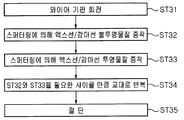
- the sputtered-slice method deposits two materials alternately using sputtering on a rotating wire substrate ST31 (ST32, ST33, ST34), and cuts them (ST35).
- ST31 rotating wire substrate
- ST35 rotating wire substrate
- This method makes it possible to fabricate a high aspect ratio structure, but it is difficult to finely control the structure and has difficulty in focusing X-rays / gamma rays at a high resolution of 20 nm or less.
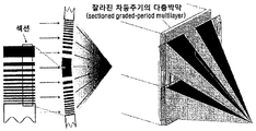
- the multilayer thin film Lauer lens (MLL) as shown in FIG. 5 is a novel technique for manufacturing a zone plate form by deposition and cutting polishing of a thin film, rather than a conventional lithography method.
- FIG. 1 As a method for manufacturing an existing MLL, there is a physical vapor deposition method as shown in FIG.
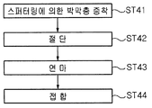
- This method produces a multilayer by the PVD method, and deposits hundreds or thousands of thin film layers corresponding to zones on a flat surface (silicon wafer) to an exact thickness by sputtering (ST41), and then cuts them.
- Deposition first deposits the outermost layer with the smallest thickness so that defects in the most important part of focusing are minimized.
- the two multilayer thin film sections face each other to complete one zone plate.
- MLL is basically the same concept as Fresnel zone plate, but due to the superiority of its manufacturing method, MLL is a new technique that goes beyond the limits of Fresnel zone plate.
- this method has a problem that it is possible to focus X-rays / gamma rays in only one direction and to produce circular focused X-rays / gamma rays because it is manufactured on a flat surface.
- An object of the present invention is to provide a method for manufacturing an X-ray / gamma-ray focusing optical system comprising a structure for X-ray / gamma-ray focusing, the thickness of the outermost layer of the structure can be adjusted by atomic layer unit and the X-ray / gamma-ray focusing optical system manufactured thereby To provide.
- the present invention also provides an X-ray / gamma focusing optical system including an outermost layer having a high aspect ratio, a structure capable of fine control, and a focusing structure having various shapes.
- an X-ray / gamma-ray focusing optical system which includes the following steps.
- the thickness of each layer may be controlled such that the first deposition layer adjacent to the inner surface of the capillary substrate has a minimum thickness, and the final deposition layer furthest from the inner surface of the capillary substrate has a maximum thickness. have.
- the atomic layer deposition may comprise the following steps:
- Removing reaction gas which is not adsorbed on the surface to be deposited inside the capillary, from the inside of the capillary among the reaction gases injected into the capillary.
- the X-ray / gamma opaque material is ruthenium (Ru), the precursor gas of the ruthenium is selected from RuCp 2 , Ru (EtCp) 2 , Ru (od) 3 and Ru (thd) 3 , the RuCp 2
- the reaction gas of is selected from air and oxygen
- the reaction gas of Ru (EtCp) 2 is selected from oxygen and NH 3 plasma
- the reaction gas of Ru (od) 3 is oxygen
- Their reaction mechanism is based on the oxidation of ruthenium precursors by oxygen or on reduction with NH 3 plasma or hydrogen.
- the X-ray / gamma opaque material is platinum (Pt)
- the precursor gas of the Pt is selected from MeCpPtMe 3 and Pt (acac) 2
- the reaction gas of MeCpPtMe 3 is selected from air, oxygen and hydrogen
- the X-ray / gamma opaque material is iridium (Ir)
- the precursor gas of Ir is Ir (acac) 3
- the reaction gas of Ir (acac) 3 may be selected from air, oxygen, and hydrogen. have.
- the X-ray / gamma opaque material is palladium (Pd)
- the precursor gas of Pd is selected from Pd (hfac) 2 , Pd (thd) 2 and Pd (keim2) 2
- the reaction gas of 2 may be selected from hydrogen and glyoxylic acid + Ar carrier
- the reaction gas of Pd (thd) 2 may be selected from hydrogen and oxygen
- the X-ray / gamma ray opaque material is rhodium (Rh)
- the precursor gas of Rh is selected from CpRh (CO) 2 and Rh (acac) 3
- the reaction gas of CpRh (CO) 2 is oxygen
- the reaction gas of Rh (acac) 3 may be oxygen.
- the X-ray / gamma transparent material may be Al 2 O 3
- the precursor gas of Al 2 O 3 may be Al (CH 3 )
- the reaction gas of Al (CH 3 ) may be H 2 O.
- the capillary substrate may have a circular or rectangular cross section.
- the capillary substrate may have a trapezoidal longitudinal section.
- the surface roughness of the inner surface of the capillary substrate may be 1 nm to 10 nm or less.
- the capillary substrate may be made of glass or quartz.
- the X-ray / gamma focusing optical system may be a Fresnel zone plate or a multilayer thin film Lauer lens.
- the thickness of the outermost layer of the structure can be controlled in atomic layers in the X-ray / gamma-focused optical system, so that the outermost layer can be manufactured as a structure having a high aspect ratio (thickness of 1 nm or less and transmission depth of 1 ⁇ m or more).
- X-ray / gamma converging optics eg, Fresnel zone
- Plates and MLL can be fabricated.
- 1 is a cross-sectional view of a typical Fresnel zone plate.
- FIG. 2 is a flow chart illustrating the fabrication of a typical Fresnel zone plate using electron beam lithography and electrochemistry.
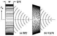
- Figure 3 shows (a) a typical Fresnel zone plate with a flat longitudinal section and (b) an ideal Fresnel zone plate with a trapezoidal longitudinal section.
- FIG. 4 is a flow chart showing the manufacturing process of a typical Fresnel zone plate using the sputtered-slice method.
- FIG. 5 is a longitudinal cross-sectional view (left) and a perspective view (right) illustrating a two-dimensional MLL to illustrate the basic concept of a typical MLL.
- PVD physical vapor deposition
- FIG. 7 is a flowchart illustrating a method of manufacturing an X-ray / gamma-focus focused optical system using atomic layer deposition according to a preferred embodiment of the present invention.
- 8A is a flow chart illustrating the deposition of X-ray / gamma-ray opaque materials by atomic layer deposition used in one preferred embodiment of the present invention.
- 8B is a flow chart illustrating the deposition of X-ray / gamma-ray transparent materials by atomic layer deposition used in one preferred embodiment of the present invention.
- FIG. 9 is a view showing a cross-section and a longitudinal section of the X-ray / gamma ray focusing optical system manufactured according to an embodiment of the present invention.
- a capillary substrate is provided (ST51), and a plurality of alternating layers of X-ray / gamma-opaque material and X-ray / gamma-ray transparent material are formed on the inner surface of the capillary substrate, respectively.
- patterns are deposited sequentially by atomic layer deposition (ST52, ST53, ST54).
- the thickness control of the outermost layer of the multilayer thin film structure that constitutes the X-ray / gamma-ray focused optical system is possible in atomic layer units, so that the high aspect ratio (the outermost layer thickness is 1 nm or less and the transmission depth is 1 ⁇ m or more) and An X-ray / gamma focused optical system having a high resolution (20 nm or less) could be manufactured.
- the deposition (ST52, ST53, ST54) of each layer of the multilayer thin film structure follows the Fresnel type. According to this, the thickness of each layer is controlled such that the first deposited layer adjacent to the inner surface of the capillary substrate has a minimum thickness in the multilayer thin film structure, and the final deposited layer furthest from the inner surface of the capillary substrate has the maximum thickness.
- each layer of the multilayer thin film structure is located at a distance from the origin by the following Fresnel type:
- r n is the position of the nth layer and f is the focal length.
- the second term may be omitted when n ⁇ ⁇ f.
- the thickness ⁇ r of the outermost layer is r n -r n-1 .
- atomic layer deposition (ST52) of an X-ray / gamma-ray opaque material constituting a plurality of alternating layers may be performed in the following order, as shown in FIG. 8A:
- a precursor gas of a deposition material formed of an X-ray / gamma-ray opaque material is injected into the capillary to adsorb the precursor gas onto the deposition target surface inside the capillary (ST61),
- Residual gas which is not adsorbed on the surface to be deposited inside the capillary among the precursor gases injected into the capillary is removed by purging from the inside of the capillary (ST62),
- Au, Ru, Pt, Pd, Rh, W, Ir, Ag, etc. (which is a material having a high electron density) may be used as the X-ray / gamma ray opaque material, and more preferably Ru, Pt, Ir , Pd, Rh may be used, most preferably Pt may be used.
- the materials described above are listed in order of being suitable as opaque materials: Au>Pt>Ir>W> Ru »Ag>Pd> Rh.
- Au is currently difficult to apply because there is no suitable precursor, and although not listed above, commonly used HfO 2 may also be used as an opaque material.
- the precursor gas for each opaque material and the reactant gas suitable for the precursor gas are described in more detail below.
- the precursor gas of ruthenium is selected from RuCp 2 , Ru (EtCp) 2 , Ru (od) 3, and Ru (thd) 3 , and the reaction of RuCp 2
- the gas is selected from air and oxygen
- the reaction gas of Ru (EtCp) 2 is selected from oxygen and NH 3 plasma
- the reaction gas of Ru (od) 3 is oxygen
- the reaction gas of Ru (thd) 3 Can be selected from air, oxygen and hydrogen.
- the precursor gas of Pt is selected from MeCpPtMe 3 and Pt (acac) 2
- the reaction gas of MeCpPtMe 3 is selected from air, oxygen, and hydrogen
- the reaction gas of Pt (acac) 2 may be selected from oxygen and hydrogen.
- the precursor gas of Ir is Ir (acac) 3
- the reaction gas of Ir (acac) 3 may be selected from air, oxygen, and hydrogen.
- the precursor gas of Pd is selected from Pd (hfac) 2 , Pd (thd) 2 and Pd (keim2) 2 , and the reaction of Pd (hfac) 2
- the gas may be selected from hydrogen and glyoxylic acid + Ar carrier, the reaction gas of Pd (thd) 2 may be selected from hydrogen and oxygen, and the reaction gas of Pd (keim2) 2 may be oxygen.
- the precursor gas of Rh is selected from CpRh (CO) 2 and Rh (acac) 3 , and the reaction gas of CpRh (CO) 2 is oxygen, and
- the reaction gas of Rh (acac) 3 may be oxygen.
- atomic layer deposition (ST53) of the X-ray / gamma-ray transparent material constituting the plurality of alternating layers is basically the same as atomic layer deposition (ST52) of the X-ray / gamma-opaque material, and the material to be deposited is X-ray.
- ST53 atomic layer deposition
- ST52 atomic layer deposition
- ST52 atomic layer deposition
- ST52 atomic layer deposition of the X-ray / gamma-ray transparent material constituting the plurality of alternating layers
- the material to be deposited is X-ray.
- the precursor gas and the reactant gas accordingly, inject the precursor gas of X-ray / gamma-opaque material into the capillary tube as shown in FIG.
- the inside of the capillary tube is removed (ST72), the reaction gas is injected into the capillary tube (ST73), and the unreacted reaction gas is removed from the inside of the capillary tube (ST74).
- the X-ray / gamma transparent material C, Al 2 O 3 , silicon nitride, etc. may be used, and more preferably Al 2 O 3 may be used, and the precursor of Al 2 O 3 used at this time
- the gas is Al (CH 3 ), and the reaction gas of Al (CH 3 ) may be H 2 O.
- the X-ray / gamma opaque material and the X-ray / gamma transparent material are repeatedly deposited alternately according to the Fresnel pattern on the inner surface of the capillary substrate by the necessary cycle, and the multilayer thin film structure is formed inside the capillary substrate.
- Form (ST54) the X-ray / gamma opaque material and the X-ray / gamma transparent material are repeatedly deposited alternately according to the Fresnel pattern on the inner surface of the capillary substrate by the necessary cycle, and the multilayer thin film structure is formed inside the capillary substrate.
- the monolayer of X-ray / gamma opaque material and the monolayer of X-ray / gamma transparent material are alternately repeated in concentric circles, and between the overall thickness, the number of cycles, and the thickness of each layer are as follows. Simple relationships can be established:
- the manufacturing method of the X-ray / gamma-focused optical system according to the present invention simply manipulates the cross-sectional shape (cross section, longitudinal section) of the capillary substrate to be used, and simply cross-sectional shape (cross section) of the multilayer thin film structure that is atomic layer deposited inside the capillary substrate And longitudinal section) can be controlled.
- the multilayer thin film structure deposited thereon also has a circular cross section (possible to fabricate a circular Fresnel zone plate and MLL).
- the multilayer thin film structure deposited thereon also has a trapezoidal profile (an ideal form of Fresnel zone plate and MLL).
- the capillary substrate used in the present invention is a physically / chemically stable material in a general atomic layer deposition process environment (150-300 ° C., a vacuum / atmospheric precursor gas), preferably made of glass, quartz, or the like. Since the surface roughness of the inner surface should be relatively small compared with the line width of the outermost layer of the zone plate, a level of 1 nm to 10 nm or less is preferable.
- a capillary substrate having a circular cross section and a trapezoidal longitudinal section is prepared.
- X-ray / gamma-opaque material and X-ray / gamma-ray transparent material are alternately and sequentially deposited by atomic layer deposition according to Fresnel type in the prepared capillary substrate to form a multilayer thin film as follows:
- the precursor gas MeCpPtMe 3 of the deposited material Pt which is an X-ray / gamma-ray opaque material, is evaporated at a temperature slightly lower than its melting point of 30 ° C.
- the vapor pressure of MeCpPtMe 3 at room temperature is relatively high. MeCpPtMe 3 reacts with air and therefore must be handled under inert gas.
- the evaporated precursor gas (MeCpPtMe 3 ) is injected into the capillary tube to adsorb the precursor gas (MeCpPtMe 3 ) onto the deposition target surface inside the capillary tube.
- N 2 is flowed into the capillary tube to remove residual gas (MeCpPtMe 3 ) which is not adsorbed on the deposition target surface of the capillary tube from the injected precursor gas (MeCpPtMe 3 ) by purging from the inside of the capillary tube.
- the reaction gas (air or O 2 ) is injected into the capillary until the X-ray / gamma-opaque layer made of Pt has a predetermined thickness according to the Fresnel type. Air or O 2 ) is adsorbed.
- oxygen used as the reaction gas, a platinum film is obtained at a temperature of 300 ° C or higher. Thermal self-decomposition of MeCpPtMe 3 becomes significant at temperatures higher than 300 ° C. Therefore 300 ° C is used as the upper temperature limit for this process. As a result, the reactivity of the precursor increases as the oxygen partial pressure increases at temperatures below 300 ° C.
- the remaining gas (Al (CH 3 )) which is not adsorbed on the surface to be deposited inside the capillary among the precursor gas (Al (CH 3 )) injected by flowing N 2 into the capillary is purged from the inside of the capillary By removing.
- reaction gas H 2 O is injected into the capillary until the X-ray / gamma transparent layer made of Al 2 O 3 has a predetermined thickness according to the Fresnel type. 2 O) is adsorbed.
- the thickness control of the outermost layer of the multilayer thin film structure is possible on an atomic layer basis so that the high aspect ratio (the thickness of the outermost layer is 1 nm or less and the transmission depth is 1 ⁇ m or more) and the high resolution (20 nm or less) It is possible to produce an ideal form of X-ray / gamma focusing optics having a circular cross section and a trapezoidal longitudinal section.
Landscapes
- Physics & Mathematics (AREA)
- Chemical & Material Sciences (AREA)
- Engineering & Computer Science (AREA)
- General Engineering & Computer Science (AREA)
- Spectroscopy & Molecular Physics (AREA)
- High Energy & Nuclear Physics (AREA)
- Nanotechnology (AREA)
- Chemical Kinetics & Catalysis (AREA)
- Mathematical Physics (AREA)
- Crystallography & Structural Chemistry (AREA)
- General Chemical & Material Sciences (AREA)
- Theoretical Computer Science (AREA)
- Materials Engineering (AREA)
- Mechanical Engineering (AREA)
- Metallurgy (AREA)
- Organic Chemistry (AREA)
- General Physics & Mathematics (AREA)
- Optics & Photonics (AREA)
- Analysing Materials By The Use Of Radiation (AREA)
Abstract
본 발명은 엑스선/감마선 집속 광학계의 제조 방법에 관한 것으로서, 모세관 기판을 제공하는 단계, 그리고 상기 모세관 기판의 내부 표면상에 각각 엑스선/감마선 불투명 물질과 엑스선/감마선 투명 물질로 이루어진 복수의 교대 층을 프레넬 형식에 따라 원자층 증착에 의해 순차적으로 퇴적하는 단계를 포함한다.
Description
본 발명은 엑스선(X-ray)/감마선(γ-ray) 집속 광학계의 제조 방법에 관한 것으로서, 보다 상세하게는 원자층 증착(atomic layer deposition)을 이용한 엑스선/감마선 집속 광학계의 제조 방법에 관련된다.
근래, 나노미터 스케일 크기를 갖는 다양한 형태의 나노 구조체들이 반도체 소자, 에너지, 디스플레이, 바이오, 의료 산업 등 전반에 걸쳐 연구, 응용되기 시작하면서, 나노 해상도의 영상화 또는 전자기파의 나노 스케일 집속이 매우 중요한 과학적 이슈가 되고 있다.
그 중에서도 특히 엑스선 현미경 기술은 그 고유의 높은 투과력, 짧은 파장과 같은 특성으로 인하여 나노 구조의 정확한 화학적, 구조적, 형태적 정보 제공 등이 가능하여, 광학 현미경이나 전자 현미경이 제공하지 못했던 물질의 상보적 정보를 제공할 수 있을 것으로 기대를 모으고 있다.
Rayleigh 가설(R=0.5λ/NA, 여기서 R은 분해능, λ는 파장, NA는 개구수)에 의하면 엑스선/감마선은 원칙적으로 엑스선/감마선의 파장과 비슷한 크기로 집속할 수 있다. 그러나 엑스선/감마선을 집속할 수 있는 광학계를 제조하는 어려움으로 인하여 현재까지 이러한 한계에 도달하지 못하고 있을 뿐만 아니라, 이론적으로 어떠한 형태의 광학계가 효과적인지 아직까지 연구가 활발하게 진행되고 있는 실정이다.
굴절률이 1보다 작고 파장 영역이 매우 짧은 엑스선을 집속하는 엑스선 집속 광학계는 일반적인 광학계가 요구하는 것보다 훨씬 까다로운 조건을 요구한다. 즉, 물질과의 상호작용이 매우 작게 되어, 아주 작은 각도만이 굴절하거나 반사한다. 다시 말하면 큰 개구수를 얻기 힘들고, 엑스선/감마선의 집속도도 매우 낮아지게 되어, 실제적으로 나노미터 스케일의 엑스선/감마선 빔을 얻는데 어려움이 많다. 전 세계적으로 엑스선/감마선 나노 집속 광학계에 대한 다양한 시도들이 있었는데, 그 중 대표적인 것으로는 프레넬 존 플레이트(Fresnel Zone Plate)와 다층박막 라우에 렌즈(Multilayer Laue Lens)를 들 수 있다.
도 1에 나타낸 바처럼, 프레넬 존 플레이트는 투명, 불투명한 원형 링(ring)이 반복적으로 나타나는 구조로, 전자기파의 회절 현상을 이용하여 광선을 집속하는 광학계의 일종이다. 일반적인 프레넬 존 플레이트는 원형 투과 격자 형태이고, 엑스선/감마선이 투과할 수 있는 투명한 층과 위상을 바꾸는 역할을 하는 불투명 층이 교대로 위치하게 된다. 이때 각각의 층에서 회절된 엑스선/감마선들이 특정 지점에서 보강 간섭이 일어나는 원리로 초점에 빔이 모아지게 된다. 각각의 층은 아래와 같은 프레넬 형식에 의하여 원점으로부터의 거리에 위치하게 된다:

여기서, rn은 n번째 층의 위치이고, f는 초점거리이다. 두 번째 항은 nλ≪f일 때 생략할 수 있다. 최외각층의 두께 Δr은 rn-rn-1이다. 프레넬 존 플레이트의 분해능은 최외각층의 두께와 거의 같다 (원형 존 플레이트의 경우는 R=1.22Δr, 선형일 경우는 R=Δr). 또한, 투과층과 흡수층 사이의 광학적 대비, 투과 깊이(빔 진행방향으로의 광학계의 크기), 각 층의 정확도, 입사빔의 근원 크기, 결맞음성 등이 분해능을 결정하는 주요한 요인이 된다.
기존의 프레넬 존 플레이트를 제조하기 위한 제조 방법으로는 전자빔 리소그래피(electron beam lithography) 및 전기화학 기술을 이용한 제조법과 스퍼터드-슬라이스(sputtered-sliced) 제조법이 있다.
존 플레이트의 집속 효율은 최외각층의 두께, 물질, 엑스선/감마선 에너지 등에 의해 영향을 받는데, 그 중에서도 특히 종횡비(aspect ratio)(즉, 최외각층의 두께와 투과 깊이의 비)에 의해 크게 좌우된다.
먼저, 도 2에 나타낸 것처럼, 전자빔 리소그래피와 전기화학 기술을 이용한 제조법은 큰 종횡비를 얻기 위하여 Si3N4 막(membrane) 위에 코팅한 감광제(PMMA, ZEP 등)(ST21)에 존 플레이트 패턴을 전자빔 리소그래피를 이용하여 제조한 후(ST22), 전기 도금법에 의하여 Au를 증착하여 존 플레이트를 완성한다(ST23).
이 방법은 현존하는 제작 기법 중 가장 고성능으로 엑스선/감마선 광학계를 제작할 수 있는 방법(20 ㎚ 수준)으로 아래에서 위로의(bottom-up) 성장 방식이다. 이 방법으로 만들어진 존 플레이트의 최외각층의 선폭은 집속된 전자빔의 크기에 의해 크게 좌우된다.
최근 기술 발전에 따라, 전자빔은 약 1 nm 이하 수준까지 집속할 수 있는 것으로 알려져 있다. 그러나 감광제의 분해능, 진동 등 장치의 안정도와 전자빔 공정 과정에서 사용되는 전자의 산란 등으로 인하여 실제로 이 방법에 의해 제작된 존 플레이트의 최외각층 두께는 현재 15 ㎚가 가장 작은 크기이다 (이때의 투과 깊이는 200 ㎚ 정도이다).
또한 이 방법을 이용할 경우, 집속 효율을 결정하는 투과 깊이는 실제적으로 1 ㎛ 이하로 제한되어, 경 엑스선/감마선에 사용되는 프레넬 존 플레이트의 집속 효율은 수%로 매우 작고, 도 3에 나타낸 바처럼, (a) 평탄한(flat) 형태의 프레넬 존 플레이트만을 제조할 수 있을 뿐 (b) 이상적 형태의 프레넬 존 플레이트는 제작할 수 없다.
그 다음, 도 4에 나타낸 것처럼, 스퍼터드-슬라이스 법은 회전하는 와이어 기판(ST31) 상에 스퍼터링을 이용하여 두 물질을 번갈아 가면서 증착하고(ST32, ST33, ST34), 이를 절단(ST35)하는 방식으로 제작한다. 이 방법은 고 종횡비의 구조물을 제조하는 것이 가능하지만, 구조를 미세하게 조절하기 힘들고, 20 ㎚ 이하의 고해상도로 엑스선/감마선을 집속하는데 어려움이 있다.
둘째, 도 5에 나타낸 바와 같은 다층박막 라우에 렌즈(MLL)는 존 플레이트 형태를 기존의 리소그래피 등의 방법의 아닌, 박막의 증착 및 절단 연마에 의하여 제조하는 새로운 기법이다.
기존의 MLL을 제조하기 위한 방법으로는, 도 6에 나타낸 것과 같은 물리적 기상 증착법(physical vapor deposition)이 있다. 이 방법은 PVD 방법으로 다층박막(multilayer)을 제작하는데, 평탄한 표면(실리콘 웨이퍼) 상에 존에 해당하는 수백 개 혹은 수천 개의 박막층을 스퍼터링 방법에 의하여 정확한 두께만큼 증착한 후(ST41), 이를 잘라서(ST42) 연마하여(ST43) 접합시키고(ST44), 엑스선/감마선을 투과시키면 회절에 의해 엑스선/감마선 빔이 초점에 모이게 된다. 증착은 가장 작은 두께를 가지는 최외각층을 먼저 증착하기 때문에 집속을 결정하는 가장 중요한 부분의 결함이 최소화되도록 한다. 두 개의 다층박막 섹션을 서로 마주보게 하여 하나의 존 플레이트를 완성하게 된다. 이 때 Bragg 회절 각 만큼(θB=0.05-0.3°) 회전하게 되면(경사형 MLL) 평탄형 MLL보다 큰 집속 효율을 얻을 수 있다. 또한 절단 연마를 통하여 빔이 통과되는 투과 깊이를 결정할 경우 매우 큰 종횡비(5 ㎚의 최외각층과 10 ㎛의 투과 깊이의 경우 종횡비는 2000임)를 얻을 수 있어 집속 효율이 일반적인 프레넬 존 플레이트 보다 수십 배 이상 증가하게 된다. 기본적으로 MLL은 일차원적 집속렌즈이기 때문에 점 접속을 위해서 두 개의 MLL을 서로 교차하여 설치하여야 한다.
MLL은 기본적으로 프레넬 존 플레이트와 같은 개념이지만, 그 제조 방법의 우수성으로 인하여 프레넬 존 플레이트의 한계를 뛰어 넘는 새로운 기법이다. 하지만, 이 방법은 평탄한 표면에 제작하기 때문에 한 방향으로만 엑스선/감마선 집속이 가능하고 원형의 집속 엑스선/감마선을 생성시키는 것이 불가능한 문제점이 있다.
본 발명의 목적은 구조물의 최외각층의 두께가 원자층 단위로 조절될 수 있는, 엑스선/감마선 집속을 위한 구조물을 포함하는 엑스선/감마선 집속 광학계의 제작 방법 및 이에 의해 제작된 엑스선/감마선 집속 광학계를 제공하는 것이다.
본 발명은 또한 고종횡비를 갖는 최외각층과 미세조절이 가능한 구조와 다양한 형태를 가질 수 있는 집속 구조물을 포함하는 엑스선/감마선 집속 광학계를 제공하는 것이다.
상기 본 발명의 목적을 달성하기 위한 본 발명의 일 측면에 따른 엑스선/감마선 집속 광학계의 제조 방법은 하기 단계를 포함한다:
모세관 기판을 제공하는 단계; 및
상기 모세관 기판의 내부 표면상에 각각 엑스선/감마선 불투명 물질과 엑스선/감마선 투명 물질로 이루어진 복수의 교대 층을 프레넬 형식에 따라 원자층 증착에 의해 순차적으로 퇴적하는 단계.
바람직하게는, 상기 퇴적 단계에서, 상기 모세관 기판의 내부 표면에 인접한 최초 퇴적층이 최소 두께를 갖고, 상기 모세관 기판의 내부 표면으로부터 가장 멀리 떨어진 최종 퇴적층이 최대 두께를 갖도록 각 층의 두께가 제어될 수 있다.
바람직하게는, 상기 원자층 증착은 하기 단계를 포함할 수 있다:
상기 엑스선/감마선 불투명 물질과 상기 엑스선/감마선 투명 물질 중에서 선택된 피증착 물질의 전구체 가스를 상기 모세관 내부에 주입하여 상기 모세관 내부의 증착 대상 표면상에 상기 전구체 가스를 흡착시키는 단계;
상기 모세관 내부에 주입된 상기 전구체 가스 중 상기 모세관 내부의 증착 대상 표면상에 흡착되지 않은 잔류 가스를 상기 모세관 내부로부터 제거하는 단계;
상기 전구체 가스와 반응하여 상기 피증착 물질에 이르게 하는 반응 가스를 상기 모세관 내부에 주입하여 상기 모세관 내부의 증착 대상 표면상에 상기 반응 가스를 흡착시키는 단계; 및
상기 모세관 내부에 주입된 상기 반응 가스 중 상기 모세관 내부의 증착 대상 표면상에 흡착되지 않은 반응 가스를 상기 모세관 내부로부터 제거하는 단계.
바람직하게는, 상기 엑스선/감마선 불투명 물질은 루테늄(Ru)이고, 상기 루테늄의 전구체 가스는 RuCp2, Ru(EtCp)2, Ru(od)3 및 Ru(thd)3 중에서 선택되고, 상기 RuCp2의 반응 가스는 공기 및 산소 중에서 선택되고, 상기 Ru(EtCp)2의 반응 가스는 산소 및 NH3 플라즈마 중에서 선택되고, 상기 Ru(od)3의 반응 가스는 산소이고, 상기 Ru(thd)3의 반응 가스는 공기, 산소 및 수소 중에서 선택될 수 있다 (여기서, Cp=시클로펜타디에닐, Et=에틸, od=2,4옥탄디오나토, thd=2,2,6,6-테트라메틸-3,5-헵탄디오나토). 이들의 반응 메커니즘은 루테늄 전구체의 산소에 의한 산화에 근거하거나, NH3 플라즈마 또는 수소에 의한 환원에 근거한다.
또한 바람직하게는, 상기 엑스선/감마선 불투명 물질은 백금(Pt)이고, 상기 Pt의 전구체 가스는 MeCpPtMe3 및 Pt(acac)2 중에서 선택되고, 상기 MeCpPtMe3의 반응 가스는 공기, 산소 및 수소 중에서 선택되고, 상기 Pt(acac)2의 반응 가스는 산소와 수소 중에서 선택될 수 있다 (여기서, Me=메틸, acac=아세틸아세토나토).
또한 바람직하게는, 상기 엑스선/감마선 불투명 물질은 이리듐(Ir)이고, 상기 Ir의 전구체 가스는 Ir(acac)3이고, 상기 Ir(acac)3의 반응 가스는 공기, 산소 및 수소 중에서 선택될 수 있다.
또한 바람직하게는, 상기 엑스선/감마선 불투명 물질은 팔라듐(Pd)이고, 상기 Pd의 전구체 가스는 Pd(hfac)2, Pd(thd)2 및 Pd(keim2)2 중에서 선택되고, 상기 Pd(hfac)2의 반응 가스는 수소 및 글리옥실산+Ar담체 중에서 선택되고, 상기 Pd(thd)2의 반응 가스는 수소 및 산소 중에서 선택되고, 상기 Pd(keim2)2의 반응 가스는 산소일 수 있다 (여기서, hfac=헥사플루오로아세틸아세토나토, keim2=[CF3C(O)CHC(NBun)CF3]-).
또한 바람직하게는, 상기 엑스선/감마선 불투명 물질은 로듐(Rh)이고, 상기 Rh의 전구체 가스는 CpRh(CO)2 및 Rh(acac)3 중에서 선택되고, 상기 CpRh(CO)2의 반응 가스는 산소이고, 상기 Rh(acac)3의 반응 가스는 산소일 수 있다.
이러한 귀금속들의 원자층 증착 조건들은 예를 들면, Titta Aaltonen의 학술논문 “Atomic Layer Deposition of Noble Metal Thin Films” (University of Helsinki, 2005)에서 보다 자세히 찾아볼 수 있다.
바람직하게는, 상기 엑스선/감마선 투명 물질은 Al2O3이고, 상기 Al2O3의 전구체 가스는 Al(CH3)이고, 상기 Al(CH3)의 반응 가스는 H2O일 수 있다.
바람직하게는, 상기 모세관 기판은 원형 또는 직사각형의 횡단면을 가질 수 있다.
바람직하게는, 상기 모세관 기판은 사다리꼴의 종단면을 가질 수 있다.
바람직하게는, 상기 모세관 기판의 내부 표면의 표면 거칠기는 1 ㎚ 내지 10 ㎚ 이하일 수 있다.
바람직하게는, 상기 모세관 기판은 유리 또는 석영으로 이루어질 수 있다.
바람직하게는 상기 엑스선/감마선 집속 광학계는 프레넬 존 플레이트 또는 다층박막 라우에 렌즈일 수 있다.
본 발명에 의하면, 엑스선/감마선 집속 광학계에 있어서 구조물의 최외각층의 두께 조절이 원자층 단위로 가능하여, 최외각층이 고종횡비(1 ㎚ 이하의 두께와 1 ㎛ 이상의 투과 깊이)를 갖는 구조물로 제작할 수 있으며, 구조물 구조의 미세 조절이 가능할 뿐만 아니라 다양한 형태(예를 들면, 원형 횡단면, 사다리꼴 종단면 등)의 엑스선/감마선 집속을 위한 구조물을 포함하는 엑스선/감마선 집속 광학계(예를 들면, 프레넬 존 플레이트 및 MLL)를 제작할 수 있다.
도 1은 전형적인 프레넬 존 플레이트의 횡단면을 나타내는 도면이다.
도 2는 전자빔 리소그래피와 전기화학법을 이용한, 전형적인 프레넬 존 플레이트의 제조 과정을 나타내는 순서도이다.
도 3는 (a) 평탄한 종단면을 갖는 전형적인 프레넬 존 플레이트와 (b) 사다리꼴의 종단면을 갖는 이상적인 프레넬 존 플레이트를 나타내는 도면이다.
도 4는 스퍼터드-슬라이스법을 이용한, 전형적인 프레넬 존 플레이트의 제조 과정을 나타내는 순서도이다.
도 5는 전형적인 MLL의 기본 개념을 설명하기 위한 종-단면도(좌)와 2차원 MLL를 설명하는 사시도(우)이다.
도 6은 물리적 기상 증착법(PVD)을 이용한, 전형적인 MLL의 제조 과정을 나타내는 순서도이다.
도 7은 본 발명의 바람직한 일 실시예에 따라 원자층 증착을 이용한 엑스선/감마선 집속 광학계의 제조 방법을 나타내는 순서도이다.
도 8a는 본 발명의 바람직한 일 실시예에서 사용되는 원자층 증착에 의한 엑스선/감마선 불투명 물질의 증착을 나타내는 순서도이다.
도 8b는 본 발명의 바람직한 일 실시예에서 사용되는 원자층 증착에 의한 엑스선/감마선 투명 물질의 증착을 나타내는 순서도이다.
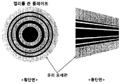
도 9는 본 발명의 바람직한 일 실시예에 따라 제조된 엑스선/감마선 집속 광학계의 횡단면과 종단면을 나타내는 도면이다.
이하 본 발명을 첨부 도면을 참고하여 보다 상세히 설명한다.
도 7을 참조하면, 본 발명에서는 모세관 기판을 제공하고(ST51), 상기 모세관 기판의 내부 표면 상에 각각 엑스선/감마선 불투명 물질과 엑스선/감마선 투명 물질로 이루어진 복수의 교대 층을 프레넬 형식(fresnel pattern)에 따라 원자층 증착에 의해 순차적으로 퇴적한다(ST52, ST53, ST54).
이러한 원자층 증착에 의해, 엑스선/감마선 집속 광학계를 이루는 다층박막 구조의 최외각층의 두께 조절이 원자층 단위로 가능해져 고종횡비(최외각층의 두께가 1 ㎚ 이하이고 투과 깊이가 1 ㎛ 이상)와 고해상도(20 ㎚ 이하)를 갖는 엑스선/감마선 집속 광학계를 제조할 수 있었다.
일반적으로 다층박막 구조의 각각의 층의 퇴적(ST52, ST53, ST54)은 프레넬 형식에 따른다. 이에 의하면, 다층박막 구조 중 상기 모세관 기판의 내부 표면에 인접한 최초 퇴적층이 최소 두께를 갖게 되고, 상기 모세관 기판의 내부 표면으로부터 가장 먼 최종 퇴적층이 최대 두께를 갖도록 각 층의 두께가 제어된다.
보다 구체적으로, 다층박막 구조의 각각의 층은 아래와 같은 프레넬 형식에 의하여 원점으로부터의 거리에 위치하게 된다:

여기서, rn은 n번째 층의 위치이고, f는 초점거리이다. 두 번째 항은 nλ≪f일 때 생략할 수 있다. 최외각층의 두께 Δr은 rn-rn-1이다. 프레넬 존 플레이트의 분해능은 최외각층의 두께와 거의 같다 (원형 존 플레이트의 경우는 R=1.22Δr, 선형일 경우는 R=Δr).
본 발명에서 복수의 교대 층을 구성하는 엑스선/감마선 불투명 물질의 원자층 증착(ST52)은, 도 8a에 나타낸 바처럼 다음 순서에 따라 이루어질 수 있다:
먼저, 엑스선/감마선 불투명 물질로 이루어지는 피증착 물질의 전구체 가스를 상기 모세관 내부에 주입하여 상기 모세관 내부의 증착 대상 표면상에 상기 전구체 가스를 흡착시키고(ST61),
상기 모세관 내부에 주입된 상기 전구체 가스 중 상기 모세관 내부의 증착 대상 표면상에 흡착되지 않은 잔류 가스를 상기 모세관 내부로부터 퍼징에 의해 제거하고(ST62),
상기 전구체 가스와 반응하여 상기 피증착 물질에 이르게 하는 반응 가스를 상기 모세관 내부에 주입하여 상기 모세관 내부의 증착 대상 표면상에 상기 반응 가스를 흡착시키고(ST63),
마지막으로, 상기 모세관 내부에 주입된 상기 반응 가스 중 상기 모세관 내부의 증착 대상 표면상에 흡착되지 않은 반응 가스를 상기 모세관 내부로부터 제거한다(ST64).
바람직하게는, 엑스선/감마선 불투명 물질로는 (높은 전자밀도를 가지는 물질인) Au, Ru, Pt, Pd, Rh, W, Ir, Ag 등이 사용될 수 있으며, 보다 바람직하게는 Ru, Pt, Ir, Pd, Rh가 사용될 수 있고, 가장 바람직하게는 Pt가 사용될 수 있다. 상기 기술된 물질을 불투명 물질로 적합한 물질 순으로 나열하면, Au > Pt > Ir > W > Ru ≫ Ag > Pd > Rh이다. 여기서, Au는 현재 적합한 precursor가 없어 아직까지는 적용되기 어렵고, 위에 나열되지는 않았으나 일반적으로 많이 사용되는 HfO2도 불투명 물질로 사용될 수 있다. 각각의 불투명 물질에 대한 전구체 가스와 그 전구체 가스에 적합한 반응 가스는 아래에서 보다 상세히 설명한다.
상기 엑스선/감마선 불투명 물질로 루테늄(Ru)을 사용할 경우, 상기 루테늄의 전구체 가스는 RuCp2, Ru(EtCp)2, Ru(od)3 및 Ru(thd)3 중에서 선택되고, 상기 RuCp2의 반응 가스는 공기 및 산소 중에서 선택되고, 상기 Ru(EtCp)2의 반응 가스는 산소 및 NH3 플라즈마 중에서 선택되고, 상기 Ru(od)3의 반응 가스는 산소이고, 상기 Ru(thd)3의 반응 가스는 공기, 산소 및 수소 중에서 선택될 수 있다.
상기 엑스선/감마선 불투명 물질로 백금(Pt)을 사용할 경우, 상기 Pt의 전구체 가스는 MeCpPtMe3 및 Pt(acac)2 중에서 선택되고, 상기 MeCpPtMe3의 반응 가스는 공기, 산소 및 수소 중에서 선택되고, 상기 Pt(acac)2의 반응 가스는 산소와 수소 중에서 선택될 수 있다.
상기 엑스선/감마선 불투명 물질로 이리듐(Ir)을 사용할 경우, 상기 Ir의 전구체 가스는 Ir(acac)3이고, 상기 Ir(acac)3의 반응 가스는 공기, 산소 및 수소 중에서 선택될 수 있다.
상기 엑스선/감마선 불투명 물질로 팔라듐(Pd)을 사용할 경우, 상기 Pd의 전구체 가스는 Pd(hfac)2, Pd(thd)2 및 Pd(keim2)2 중에서 선택되고, 상기 Pd(hfac)2의 반응 가스는 수소 및 글리옥실산+Ar담체 중에서 선택되고, 상기 Pd(thd)2의 반응 가스는 수소 및 산소 중에서 선택되고, 상기 Pd(keim2)2의 반응 가스는 산소일 수 있다.
상기 엑스선/감마선 불투명 물질로 로듐(Rh)을 사용할 경우, 상기 Rh의 전구체 가스는 CpRh(CO)2 및 Rh(acac)3 중에서 선택되고, 상기 CpRh(CO)2의 반응 가스는 산소이고, 상기 Rh(acac)3의 반응 가스는 산소일 수 있다.
그 다음, 본 발명에서 복수의 교대 층을 구성하는 엑스선/감마선 투명 물질의 원자층 증착(ST53)은 기본적으로 상기 엑스선/감마선 불투명 물질의 원자층 증착(ST52)과 동일하되, 피증착 물질을 엑스선/감마선 투명 물질로 교체하고, 이에 맞게 전구체 가스와 반응 가스를 변경하여, 도 8b에 나타낸 바처럼, 모세관 내부에 엑스선/감마선 불투명 물질의 전구체 가스를 주입하고(ST71), 흡착되지 않은 전구체를 가스 모세관 내부에서 제거(ST72)하고, 모세관 내부에 반응 가스를 주입하고(ST73), 반응하지 않은 반응 가스를 모세관 내부에서 제거한다(ST74).
바람직하게는, 엑스선/감마선 투명 물질로는 C, Al2O3, 실리콘 나이트라이드 등이 사용될 수 있으며, 보다 바람직하게는 Al2O3가 사용될 수 있고, 이 때 사용되는 Al2O3의 전구체 가스는 Al(CH3)이고, Al(CH3)의 반응 가스는 H2O가 사용될 수 있다.
이렇게, 원자층 증착을 이용하여 모세관 기판의 내부 표면상에 엑스선/감마선 불투명 물질과 엑스선/감마선 투명 물질을 프레넬 패턴에 따라 교대로 필요한 사이클만큼 반복 퇴적하여, 상기 모세관 기판의 내부에 다층박막 구조를 형성하게 된다(ST54).
이 다층박막 구조는 엑스선/감마선 불투명 물질의 단원자층과 엑스선/감마선 투명 물질의 단원자층이 동심원을 이루며 교대로 반복되며, 다층박막 구조의 전체 두께, 사이클 수 그리고 각 층의 두께 사이에는 다음과 같은 간단한 관계식이 성립될 수 있다:

유리하게도, 본 발명에 따른 엑스선/감마선 집속 광학계의 제조 방법은 사용되는 상기 모세관 기판의 단면 형태(횡단면, 종단면)만을 조작하여, 간단히 모세관 기판 내부에 원자층 증착되는 다층박막 구조의 단면 형태(횡단면과 종단면)를 제어할 수 있다.
예를 들면, 모세관 기판이 원형의 횡단면을 가질 경우, 그 내부에 원자층 증착되는 다층박막 구조 역시 이에 대응하여 원형의 횡단면을 가지게 되며 (원형의 프레넬 존 플레이트와 MLL 제작 가능), 모세관 기판의 사다리꼴의 종단면을 가질 경우, 도 9에 나타낸 것처럼, 그 내부에 원자층 증착되는 다층박막 구조 역시 이에 대응하여 사다리꼴의 종단면(이상적인 형태의 프레넬 존 플레이트와 MLL 제작 가능)을 가지게 된다.
본 발명에 사용되는 모세관 기판은 일반적인 원자층 증착 공정 환경(150-300℃, 진공/대기압의 전구체 가스)에서 물리적/화학적으로 안정적인 물질로, 유리 또는 석영 등으로 이루어지는 것이 바람직하고, 상기 모세관 기판의 내부 표면의 표면 거칠기는, 존 플레이트 최외각층의 선폭에 비해 상대적으로 작아야 하므로, 1 ㎚ 내지 10 ㎚ 이하의 수준이 바람직하다.
실시예
1. 모세관 기판 준비
일반적인 원자층 증착 공정 환경(150-300℃, 진공/대기압의 전구체 가스)에서 물리적/화학적으로 안정적인 물질로, 유리 또는 석영 등으로 이루어지고, 내부 표면의 표면 거칠기가 1 ㎚ 내지 10 ㎚ 이하 수준이고, 원형의 횡단면과 사다리꼴의 종단면을 갖는 모세관 기판을 준비한다.
2. 원자층 증착에 의한 다층박막의 형성
준비된 모세관 기판 내부에 아래와 같이 엑스선/감마선 불투명 물질과 엑스선/감마선 투명 물질을 프레넬 형식에 따라 원자층 증착에 의해 교대로 반복하여 순차적으로 퇴적하여 다층박막을 형성한다:
(1) 엑스선/감마선 불투명 물질 증착
엑스선/감마선 불투명 물질인 피증착 물질 Pt의 전구체 가스 MeCpPtMe3를 이의 융점인 30℃보다 약간 낮은 상온에서 증발시킨다. 상온에서의MeCpPtMe3의 증기압은 비교적 높다. MeCpPtMe3는 공기와 반응하므로 불활성 가스 하에서 취급되어야한다. 상기 증발된 전구체 가스(MeCpPtMe3)를 상기 모세관 내부에 주입하여 상기 모세관 내부의 증착 대상 표면상에 상기 전구체 가스(MeCpPtMe3)를 흡착시킨다.
상기 모세관 내부에 N2를 흐르게 하여 상기 주입된 전구체 가스(MeCpPtMe3) 중 상기 모세관 내부의 증착 대상 표면상에 흡착되지 않은 잔류 가스(MeCpPtMe3)를 상기 모세관 내부로부터 퍼징에 의해 제거한다.
Pt로 이루어진 엑스선/감마선 불투명층이 프레넬 형식에 따른 소정의 두께가 될 때까지, 반응 가스(공기 또는 O2)를 상기 모세관 내부에 주입하여 상기 모세관 내부의 증착 대상 표면상에 상기 반응 가스(공기 또는 O2)를 흡착시킨다. 산소를 반응 가스로 사용할 때, 300℃ 이상의 온도에서 백금 막이 얻어진다. MeCpPtMe3의 열적 자기-분해는 300℃보다 높은 온도에서 현저해 진다. 따라서 300℃를 이 공정에 대한 온도 상한으로 삼는다. 따라서 결과적으로 300℃보다 낮은 온도에서 산소 분압이 증가함에 따라 전구체의 반응성이 증가한다.
상기 모세관 내부에 N2를 흐르게 하여 주입된 상기 반응 가스(공기 또는 O2) 중 상기 모세관 내부의 증착 대상 표면상에 흡착되지 않은 반응 가스(공기 또는 O2)를 상기 모세관 내부로부터 퍼징에 의해 제거한다.
(2) 엑스선/감마선 투명 물질 증착
엑스선/감마선 투명 물질인 피증착 물질 Al2O3의 전구체 가스 Al(CH3)를 상기 모세관 내부에 주입하여 상기 모세관 내부의 증착 대상 표면상에 상기 전구체 가스(Al(CH3))를 흡착시킨다.
상기 모세관 내부에 N2를 흐르게 하여 주입된 상기 전구체 가스(Al(CH3)) 중 상기 모세관 내부의 증착 대상 표면상에 흡착되지 않은 잔류 가스(Al(CH3))를 상기 모세관 내부로부터 퍼징에 의해 제거한다.
Al2O3로 이루어진 엑스선/감마선 투명층이 프레넬 형식에 따른 소정의 두께가 될 때까지, 반응 가스 H2O를 상기 모세관 내부에 주입하여 상기 모세관 내부의 증착 대상 표면상에 상기 반응 가스(H2O)를 흡착시킨다.
상기 모세관 내부에 N2를 흐르게 하여 주입된 상기 반응 가스(H2O) 중 상기 모세관 내부의 증착 대상 표면상에 흡착되지 않은 반응 가스(H2O)를 상기 모세관 내부로부터 제거한다.
(3) 다층박막 구조 형성
(1)과 (2) 절차를 교대로 필요한 사이클만큼 반복함으로써 모세관 기판 내부에 다층박막 구조를 형성한다.
본 발명의 바람직한 일 실시예에 따르면 다층박막 구조의 최외각층의 두께 조절이 원자층 단위로 가능해져 고종횡비(최외각층의 두께가 1 ㎚ 이하이고 투과 깊이가 1 ㎛ 이상)와 고해상도(20 ㎚ 이하)를 가질 뿐만 아니라 원형의 횡단면 및 사다리꼴의 종단면을 갖는 이상적인 형태의 엑스선/감마선 집속 광학계를 제조할 수 있다.
Claims (14)
- 엑스선/감마선 집속 광학계의 제조 방법으로서,모세관 기판을 제공하는 단계; 및상기 모세관 기판의 내부 표면상에 각각 엑스선/감마선 불투명 물질과 엑스선/감마선 투명 물질로 이루어진 복수의 교대 층을 프레넬 형식에 따라 원자층 증착에 의해 순차적으로 퇴적하는 단계;를 포함하는 엑스선/감마선 광학계의 제조 방법.
- 제1항에 있어서, 상기 퇴적 단계에서, 상기 모세관 기판의 내부 표면에 인접한 최초 퇴적층이 최소 두께를 갖고, 상기 모세관 기판의 내부 표면으로부터 가장 멀리 떨어진 최종 퇴적층이 최대 두께를 갖도록 각 층의 두께가 제어되는 것을 특징으로 하는 엑스선/감마선 집속 광학계의 제조 방법.
- 제1항에 있어서, 상기 원자층 증착은,상기 엑스선/감마선 불투명 물질과 상기 엑스선/감마선 투명 물질 중에서 선택된 피증착 물질의 전구체 가스를 상기 모세관 내부에 주입하여 상기 모세관 내부의 증착 대상 표면상에 상기 전구체 가스를 흡착시키는 단계;상기 모세관 내부에 주입된 상기 전구체 가스 중 상기 모세관 내부의 증착 대상 표면상에 흡착되지 않은 잔류 가스를 상기 모세관 내부로부터 제거하는 단계;상기 전구체 가스와 반응하여 상기 피증착 물질에 이르게 하는 반응 가스를 상기 모세관 내부에 주입하여 상기 모세관 내부의 증착 대상 표면상에 상기 반응 가스를 흡착시키는 단계; 및상기 모세관 내부에 주입된 상기 반응 가스 중 상기 모세관 내부의 증착 대상 표면상에 흡착되지 않은 반응 가스를 상기 모세관 내부로부터 제거하는 단계;를 포함하는 엑스선/감마선 집속 광학계의 제조 방법.
- 제3항에 있어서, 상기 엑스선/감마선 불투명 물질은 루테늄(Ru)이고, 상기 루테늄의 전구체 가스는 RuCp2, Ru(EtCp)2, Ru(od)3 및 Ru(thd)3 중에서 선택되고, 상기 RuCp2의 반응 가스는 공기 및 산소 중에서 선택되고, 상기 Ru(EtCp)2의 반응 가스는 산소 및 NH3 플라즈마 중에서 선택되고, 상기 Ru(od)3의 반응 가스는 산소이고, 상기 Ru(thd)3의 반응 가스는 공기, 산소 및 수소 중에서 선택되는 것을 특징으로 하는 엑스선/감마선 집속 광학계의 제조 방법.
- 제3항에 있어서, 상기 엑스선/감마선 불투명 물질은 백금(Pt)이고, 상기 Pt의 전구체 가스는 MeCpPtMe3 및 Pt(acac)2 중에서 선택되고, 상기 MeCpPtMe3의 반응 가스는 공기, 산소 및 수소 중에서 선택되고, 상기 Pt(acac)2의 반응 가스는 산소와 수소 중에서 선택되는 것을 특징으로 하는 엑스선/감마선 집속 광학계의 제조 방법.
- 제3항에 있어서, 상기 엑스선/감마선 불투명 물질은 이리듐(Ir)이고, 상기 Ir의 전구체 가스는 Ir(acac)3이고, 상기 Ir(acac)3의 반응 가스는 공기, 산소 및 수소 중에서 선택되는 것을 특징으로 하는 엑스선/감마선 집속 광학계의 제조 방법.
- 제3항에 있어서, 상기 엑스선/감마선 불투명 물질은 팔라듐(Pd)이고, 상기 Pd의 전구체 가스는 Pd(hfac)2,Pd(thd)2 및 Pd(keim2)2 중에서 선택되고, 상기 Pd(hfac)2의 반응 가스는 수소 및 글리옥실산+Ar담체 중에서 선택되고, 상기 Pd(thd)2의 반응 가스는 수소 및 산소 중에서 선택되고, 상기 Pd(keim2)2의 반응 가스는 산소인 것을 특징으로 하는 엑스선/감마선 집속 광학계의 제조 방법.
- 제3항에 있어서, 상기 엑스선/감마선 불투명 물질은 로듐(Rh)이고, 상기 Rh의 전구체 가스는 CpRh(CO)2 및 Rh(acac)3 중에서 선택되고, 상기 CpRh(CO)2의 반응 가스는 산소이고, 상기 Rh(acac)3의 반응 가스는 산소인 것을 특징으로 하는 엑스선/감마선 집속 광학계의 제조 방법.
- 제3항에 있어서, 상기 엑스선/감마선 투명 물질은 Al2O3이고, 상기 Al2O3의 전구체 가스는 Al(CH3)이고, 상기 Al(CH3)의 반응 가스는 H2O인 것을 특징으로 하는 엑스선/감마선 집속 광학계의 제조 방법.
- 제3항에 있어서, 상기 모세관 기판은 원형 또는 직사각형의 횡단면을 갖는 것을 특징으로 하는 엑스선/감마선 집속 광학계의 제조 방법.
- 제3항에 있어서, 상기 모세관 기판은 사다리꼴의 종단면을 갖는 것을 특징으로 하는 엑스선/감마선 집속 광학계의 제조 방법.
- 제3항에 있어서, 상기 모세관 기판의 내부 표면의 표면 거칠기는 1 ㎚ 내지 10 ㎚ 이하인 것을 특징으로 하는 엑스선/감마선 집속 광학계의 제조 방법.
- 제1항에 있어서, 상기 모세관 기판은 유리 또는 석영으로 이루어지는 것을 특징으로 하는 엑스선/감마선 집속 광학계의 제조 방법.
- 제1항 내지 제13항 중 어느 한 항에 있어서, 상기 엑스선/감마선 집속 광학계는 프레넬 존 플레이트 또는 다층박막 라우에 렌즈인 것을 특징으로 하는 엑스선/감마선 집속 광학계의 제조 방법.
Priority Applications (1)
| Application Number | Priority Date | Filing Date | Title |
|---|---|---|---|
| US13/976,634 US9366786B2 (en) | 2010-12-29 | 2011-10-28 | Method for manufacturing X-ray/γ-ray focusing optical system using atomic layer deposition |
Applications Claiming Priority (2)
| Application Number | Priority Date | Filing Date | Title |
|---|---|---|---|
| KR10-2010-0138051 | 2010-12-29 | ||
| KR1020100138051A KR101195415B1 (ko) | 2010-12-29 | 2010-12-29 | 원자층 증착을 이용한 엑스선(Xray)/감마선(γray)집속 광학계의 제조방법 |
Publications (1)
| Publication Number | Publication Date |
|---|---|
| WO2012091269A1 true WO2012091269A1 (ko) | 2012-07-05 |
Family
ID=46383314
Family Applications (1)
| Application Number | Title | Priority Date | Filing Date |
|---|---|---|---|
| PCT/KR2011/008143 Ceased WO2012091269A1 (ko) | 2010-12-29 | 2011-10-28 | 원자층 증착을 이용한 엑스선/감마선 집속 광학계의 제조 방법 |
Country Status (3)
| Country | Link |
|---|---|
| US (1) | US9366786B2 (ko) |
| KR (1) | KR101195415B1 (ko) |
| WO (1) | WO2012091269A1 (ko) |
Families Citing this family (7)
| Publication number | Priority date | Publication date | Assignee | Title |
|---|---|---|---|---|
| US9859028B2 (en) * | 2012-03-08 | 2018-01-02 | Max-Planck-Gesellschaft Zur Foerderung Der Wissenschaften E.V. | Method of producing a Fresnel Zone Plate for applications in high energy radiation |
| US10183375B2 (en) | 2016-03-02 | 2019-01-22 | Alcorix Co. | Batch-processing method for super-high aspect ratio diffractive optics |
| US10816705B2 (en) | 2016-03-02 | 2020-10-27 | Alcorix Co. | Super-high aspect ratio diffractive optics fabricated by batch-processing |
| EP3282294B1 (en) * | 2016-08-12 | 2020-04-15 | Max-Planck-Gesellschaft zur Förderung der Wissenschaften e.V. | High resolution full material fresnel zone plate array and process for its fabrication |
| WO2020137047A1 (ja) * | 2018-12-28 | 2020-07-02 | 株式会社堀場製作所 | X線導管の製造方法、x線導管、分析装置 |
| EP3996112B1 (en) * | 2020-11-06 | 2024-05-01 | Deutsches Elektronen-Synchrotron DESY | Method for producing a multilayer laue lens |
| CN113345618B (zh) * | 2021-06-09 | 2023-02-28 | 中国科学院电工研究所 | 一种x射线光学元件的制备方法及系统 |
Citations (3)
| Publication number | Priority date | Publication date | Assignee | Title |
|---|---|---|---|---|
| JPH0784096A (ja) * | 1993-09-13 | 1995-03-31 | Nikon Corp | X線照明用ゾーンプレート |
| JPH07120597A (ja) * | 1993-10-26 | 1995-05-12 | Nikon Corp | 2次回折用ゾーンプレート及び軟x線顕微鏡 |
| JP2002350593A (ja) * | 2001-05-23 | 2002-12-04 | National Institute Of Advanced Industrial & Technology | X線集光方法及びx線集光装置 |
Family Cites Families (6)
| Publication number | Priority date | Publication date | Assignee | Title |
|---|---|---|---|---|
| JP4197195B2 (ja) * | 1998-02-27 | 2008-12-17 | ヒューレット・パッカード・カンパニー | 音声情報の提供方法 |
| JP2003338447A (ja) * | 2002-05-21 | 2003-11-28 | Mitsubishi Electric Corp | X線マスク、x線露光装置、x線露光方法およびこのx線露光方法で製造された半導体装置 |
| US7019304B2 (en) * | 2003-10-06 | 2006-03-28 | General Electric Company | Solid-state radiation imager with back-side irradiation |
| US7365918B1 (en) * | 2004-08-10 | 2008-04-29 | Xradia, Inc. | Fast x-ray lenses and fabrication method therefor |
| US7713907B2 (en) * | 2006-03-06 | 2010-05-11 | Uchicago Argonne, Llc | Method of preparing size-selected metal clusters |
| US20100227476A1 (en) * | 2009-03-04 | 2010-09-09 | Peck John D | Atomic layer deposition processes |
-
2010
- 2010-12-29 KR KR1020100138051A patent/KR101195415B1/ko not_active Expired - Fee Related
-
2011
- 2011-10-28 WO PCT/KR2011/008143 patent/WO2012091269A1/ko not_active Ceased
- 2011-10-28 US US13/976,634 patent/US9366786B2/en not_active Expired - Fee Related
Patent Citations (3)
| Publication number | Priority date | Publication date | Assignee | Title |
|---|---|---|---|---|
| JPH0784096A (ja) * | 1993-09-13 | 1995-03-31 | Nikon Corp | X線照明用ゾーンプレート |
| JPH07120597A (ja) * | 1993-10-26 | 1995-05-12 | Nikon Corp | 2次回折用ゾーンプレート及び軟x線顕微鏡 |
| JP2002350593A (ja) * | 2001-05-23 | 2002-12-04 | National Institute Of Advanced Industrial & Technology | X線集光方法及びx線集光装置 |
Also Published As
| Publication number | Publication date |
|---|---|
| KR101195415B1 (ko) | 2012-10-29 |
| US9366786B2 (en) | 2016-06-14 |
| US20130280421A1 (en) | 2013-10-24 |
| KR20120092745A (ko) | 2012-08-22 |
Similar Documents
| Publication | Publication Date | Title |
|---|---|---|
| KR101195415B1 (ko) | 원자층 증착을 이용한 엑스선(Xray)/감마선(γray)집속 광학계의 제조방법 | |
| US20110222179A1 (en) | Micromirror arrays having self aligned features | |
| WO1996007954A1 (en) | Microstructures and methods for manufacturing microstructures | |
| US20130140269A1 (en) | Method and mechanism of photoresist layer structure used in manufacturing nano scale patterns | |
| Saitoh et al. | Characterization of sliced multilayer zone plates for hard x rays | |
| Zhao et al. | The recent development of soft x-ray interference lithography in SSRF | |
| US9640291B2 (en) | Stacked zone plates for pitch frequency multiplication | |
| US20220057353A1 (en) | Light-activated gas sensor based on 3d nanostructure operable at low temperature with high performance and method for manufacturing the same | |
| US20210239889A1 (en) | High Resolution Full Material Fresnel Zone Plate Array and Process for its Fabrication | |
| KR20240127566A (ko) | 나노튜브를 기반으로 하는 극자외선 노광용 펠리클 및 그의 제조 방법 | |
| WO2018194184A1 (en) | Nanoplasmonic instrumentation, materials, methods and system integration | |
| US20100033702A1 (en) | Coated mirrors and their fabrication | |
| CN109116454B (zh) | 光栅的制备方法 | |
| Mojarad et al. | Fabrication of high aspect ratio and tilted nanostructures using extreme ultraviolet and soft x-ray interference lithography | |
| WO2020204285A1 (ko) | 3차원 나노구조의 고정상을 갖는 가스 크로마토그래피용 마이크로 분별기 및 그 제조 방법 | |
| CN116904966A (zh) | 制造用于euv光刻的衬底和反射光学元件的方法 | |
| Nachimuthu et al. | Performance characteristics of beamline 6.3. 1 from 200 eV to 2000 eV at the Advanced Light Source | |
| WO2017183941A1 (ko) | Euv 펠리클 구조체, 및 그 제조 방법 | |
| Kamijo et al. | Fabrication and testing of hard x‐ray sputtered‐sliced zone plate | |
| JP3923180B2 (ja) | X線用光学素子およびその製造方法 | |
| Yurgens et al. | Measurement and compensation of misalignment in double-sided hard X-ray Fresnel zone plates | |
| HK1052793A1 (zh) | X射線變焦鏡頭 | |
| US11966068B2 (en) | Inorganic wave plate and manufacturing method therefor | |
| FI20225350A1 (en) | A free-standing pellicle film comprising harm-structures | |
| Babin et al. | Fabrication of diffraction X-ray elements |
Legal Events
| Date | Code | Title | Description |
|---|---|---|---|
| 121 | Ep: the epo has been informed by wipo that ep was designated in this application |
Ref document number: 11852976 Country of ref document: EP Kind code of ref document: A1 |
|
| WWE | Wipo information: entry into national phase |
Ref document number: 13976634 Country of ref document: US |
|
| NENP | Non-entry into the national phase |
Ref country code: DE |
|
| 122 | Ep: pct application non-entry in european phase |
Ref document number: 11852976 Country of ref document: EP Kind code of ref document: A1 |