WO2012090772A1 - 蒸着装置、削具および蒸着材料の回収方法 - Google Patents
蒸着装置、削具および蒸着材料の回収方法 Download PDFInfo
- Publication number
- WO2012090772A1 WO2012090772A1 PCT/JP2011/079442 JP2011079442W WO2012090772A1 WO 2012090772 A1 WO2012090772 A1 WO 2012090772A1 JP 2011079442 W JP2011079442 W JP 2011079442W WO 2012090772 A1 WO2012090772 A1 WO 2012090772A1
- Authority
- WO
- WIPO (PCT)
- Prior art keywords
- vapor deposition
- deposited
- vapor
- deposition
- particles
- Prior art date
- Legal status (The legal status is an assumption and is not a legal conclusion. Google has not performed a legal analysis and makes no representation as to the accuracy of the status listed.)
- Ceased
Links
Images



Classifications
-
- C—CHEMISTRY; METALLURGY
- C23—COATING METALLIC MATERIAL; COATING MATERIAL WITH METALLIC MATERIAL; CHEMICAL SURFACE TREATMENT; DIFFUSION TREATMENT OF METALLIC MATERIAL; COATING BY VACUUM EVAPORATION, BY SPUTTERING, BY ION IMPLANTATION OR BY CHEMICAL VAPOUR DEPOSITION, IN GENERAL; INHIBITING CORROSION OF METALLIC MATERIAL OR INCRUSTATION IN GENERAL
- C23C—COATING METALLIC MATERIAL; COATING MATERIAL WITH METALLIC MATERIAL; SURFACE TREATMENT OF METALLIC MATERIAL BY DIFFUSION INTO THE SURFACE, BY CHEMICAL CONVERSION OR SUBSTITUTION; COATING BY VACUUM EVAPORATION, BY SPUTTERING, BY ION IMPLANTATION OR BY CHEMICAL VAPOUR DEPOSITION, IN GENERAL
- C23C14/00—Coating by vacuum evaporation, by sputtering or by ion implantation of the coating forming material
- C23C14/04—Coating on selected surface areas, e.g. using masks
- C23C14/042—Coating on selected surface areas, e.g. using masks using masks
-
- C—CHEMISTRY; METALLURGY
- C23—COATING METALLIC MATERIAL; COATING MATERIAL WITH METALLIC MATERIAL; CHEMICAL SURFACE TREATMENT; DIFFUSION TREATMENT OF METALLIC MATERIAL; COATING BY VACUUM EVAPORATION, BY SPUTTERING, BY ION IMPLANTATION OR BY CHEMICAL VAPOUR DEPOSITION, IN GENERAL; INHIBITING CORROSION OF METALLIC MATERIAL OR INCRUSTATION IN GENERAL
- C23C—COATING METALLIC MATERIAL; COATING MATERIAL WITH METALLIC MATERIAL; SURFACE TREATMENT OF METALLIC MATERIAL BY DIFFUSION INTO THE SURFACE, BY CHEMICAL CONVERSION OR SUBSTITUTION; COATING BY VACUUM EVAPORATION, BY SPUTTERING, BY ION IMPLANTATION OR BY CHEMICAL VAPOUR DEPOSITION, IN GENERAL
- C23C14/00—Coating by vacuum evaporation, by sputtering or by ion implantation of the coating forming material
- C23C14/22—Coating by vacuum evaporation, by sputtering or by ion implantation of the coating forming material characterised by the process of coating
- C23C14/24—Vacuum evaporation
Definitions
- the present invention relates to a vapor deposition apparatus, a cutting tool, and a method for collecting vapor deposition material for collecting vapor deposition material deposited on unnecessary portions.
- the core component of the electronic device include a semiconductor, a flat display panel including a liquid crystal panel, a solar cell, a semiconductor device, and a memory.
- Such an electronic device is manufactured using a vacuum film forming apparatus using a vacuum film forming method such as a sputtering method, a vacuum vapor deposition method, or an ion plating method, and a rare metal is often used as a film forming material.
- a vacuum film forming method such as a sputtering method, a vacuum vapor deposition method, or an ion plating method
- a rare metal is often used as a film forming material.
- flat panel displays have been used in various products and fields, and further flat panel displays are required to have larger sizes, higher image quality, and lower power consumption.
- an organic EL display device including an organic EL element using electroluminescence (electroluminescence; hereinafter referred to as “EL”) of an organic material is an all-solid-state type, driven at a low voltage and has a high-speed response.
- EL electroluminescence
- the organic EL display device has, for example, a configuration in which an organic EL element connected to a TFT is provided on a substrate made of a glass substrate or the like provided with a TFT (thin film transistor).
- the organic EL element is a light emitting element that can emit light with high luminance by low-voltage direct current drive, and has a structure in which a first electrode, an organic EL layer, and a second electrode are stacked in this order. Of these, the first electrode is connected to the TFT.
- the organic EL layer a hole injection layer, a hole transport layer, an electron blocking layer, a light emitting layer, a hole blocking layer, an electron transport layer, an electron injection layer
- a hole injection layer a hole injection layer, a hole transport layer, an electron blocking layer, a light emitting layer, a hole blocking layer, an electron transport layer, an electron injection layer
- a full-color organic EL display device is generally formed by arranging organic EL elements of red (R), green (G), and blue (B) as sub-pixels on a substrate, and using TFTs. Image display is performed by selectively emitting light from these organic EL elements with a desired luminance.
- the organic EL element in the light emitting portion of such an organic EL display device is generally formed by stacking organic films.
- a light emitting layer made of an organic light emitting material that emits light of each color is formed in a predetermined pattern for each organic EL element that is a light emitting element.
- a vacuum evaporation method using an evaporation mask called a “shadow mask”, an ink jet method, a laser transfer method, or the like can be applied to film formation of a predetermined pattern by stacked evaporation.
- crucible or “boat”, which is a deposition material storage unit that is provided in a deposition source and stores a deposition material inside, is heated under high vacuum.
- the vapor deposition material is deposited on the deposition target substrate by sublimation.
- the vapor deposition material injected from the vapor deposition material container as vapor deposition particles is vapor-deposited through an opening provided in the vapor deposition mask in a vacuum chamber of a vacuum vapor deposition apparatus, thereby forming a desired film formation pattern. Can be obtained.
- the organic EL element in the light emitting part of the organic EL display device is formed by stacking organic films.
- the scattered vapor deposition particles also adhere to components other than the deposition target substrate such as a TFT substrate. .
- the vacuum chamber of the vacuum deposition apparatus there are various components such as a deposition plate and a shutter.
- the organic material constituting the organic film is expensive, but the vapor deposition material adhering to these components, that is, the vapor deposition particles adhering to other than the film formation substrate such as the TFT substrate is wasted unless it is collected.
- material utilization efficiency shows the ratio of the material actually utilized among the materials used at the time of vapor deposition.
- Patent Document 1 discloses a method of heating and re-evaporating the vapor deposition material attached to the cell shutter and cooling and recovering the vapor with a shroud in which a cooling medium is circulated.
- Patent Document 2 discloses a method in which a vapor deposition material adhering to a shutter plate is heated and melted by a heater in the shutter, dropped into a vapor deposition source, and recovered.
- Patent Document 3 discloses a method of heating a cell shutter with a heater to evaporate vapor deposition material adhering to the lower surface of the cell shutter and recovering it in a crucible.
- a vapor deposition material recovery tool having a blocking wall and a vapor flow discharge port is arranged so as to cover the vapor outlet, and the divergence angle of the vapor flow from the vapor deposition source to the substrate to be processed is controlled. After vapor deposition, a method is disclosed in which the vapor deposition material recovery tool is taken out and the vapor deposition material deposited on the barrier wall is recovered.
- Patent Document 5 discloses that components such as a shutter in a chamber in which an organic material is deposited are made inactive materials that do not change the organic material, and the organic material deposited on these components is recovered.
- Patent Document 6 discloses a method for collecting deposits on a film forming jig by spraying a water jet.
- JP 2008-127642 A released on June 5, 2008
- JP 2008-88465 released on April 17, 2008
- JP 2008-223102 A published September 25, 2008
- JP 2002-190389 A released July 5, 2002
- JP 2002-292346 A released on October 8, 2002
- Patent Documents 1 to 3 have a problem that the vapor deposition material attached to portions other than the shutter cannot be recovered.
- the heating of the vapor deposition material may cause a deterioration of the vapor deposition material due to the heating.
- Patent Document 4 has a problem that the material attached to other than the blocking wall and the substrate to be processed cannot be recovered.
- Patent Document 5 discloses that an organic material deposited on a part such as a shutter in the chamber is recovered, but a specific recovery method is not disclosed.
- Patent Document 6 cannot be applied to a vapor deposition material that is easily denatured by moisture. Moreover, even with water, the film forming jig is damaged or peeled off by water pressure, and the peeled film forming jig is mixed into the peeled vapor deposition material. However, no mention is made of impurities mixed in this way.
- the conventional method could not collect the film forming material efficiently and at low cost.
- the present invention has been made in view of the above-described problems, and an object of the present invention is to provide a vapor deposition apparatus, a cutting tool, and a vapor deposition material collection method that can collect the vapor deposition material efficiently and at low cost. .
- the vapor deposition apparatus of the present invention is a vapor deposition apparatus that deposits vapor deposition particles released from a vapor deposition material storage unit provided in a vapor deposition source on a substrate in a vapor deposition chamber,
- the temperature of the vapor deposition material storage unit is set so that the vapor deposition material stored in the vapor deposition material storage unit is in a temperature region in which the vapor deposition material is not decomposed and a predetermined vapor deposition rate is obtained.
- the vapor deposition particles released in the first direction are vapor-deposited on the substrate, and the second deposition direction is different from the first direction during the first period from the deposition material storage unit.
- the vapor deposition particles released or the vapor deposition particles released from the vapor deposition material storage unit are vapor-deposited on an adhesion preventing member that can be removed from the vapor deposition apparatus.
- the member at least the steam At least a portion of the surface of the particles is deposited, at a maximum temperature below the above temperature range is characterized in that it consists of a material which does not have a melting point and sublimation point.
- the cutting tool of the present invention is capable of scraping and peeling the deposited film deposited on the surface of the deposition member provided in the deposition apparatus, and at least the surface of the deposition member.
- the portion in contact with the deposited film deposited on the substrate is characterized in that the hardness is higher than that of the deposition preventing member.
- At least a part of the surface on which the vapor deposition particles are vapor-deposited in the anti-adhesion member is made of a material having no melting point and sublimation point at the maximum temperature or lower in the temperature region.
- the deposited film deposited on the surface of the deposition preventing member provided in the deposition apparatus is shaved. In the case of peeling, only the material having no melting point and sublimation point and the vapor deposition material can be recovered below the maximum temperature in the above temperature range.
- the recovered material consisting only of the material having no melting point and sublimation point and the vapor deposition material can be directly put into the vapor deposition material storage section and reused.
- the vapor deposition material can be recovered efficiently and at low cost.
- the cutting tool of the present invention is an adhesion member for a vapor deposition apparatus that vapor-deposits vapor deposition particles released from a vapor deposition material storage unit provided in a vapor deposition source on a substrate in a vapor deposition chamber.
- the vapor deposition particles released in the first direction are vapor-deposited on the substrate, and the vapor deposition material storage unit supplies the vapor deposition particles.
- the portion of the cutting tool that is vapor-deposited on the material and in contact with at least the vapor-deposited film vapor-deposited on the surface of the adhesion-preventing member is made of a material that does not have a melting point and a sublimation point below the maximum temperature in the temperature range. It is characterized by that.
- the vapor deposition material recovery method of the present invention includes the vapor deposition apparatus according to any one of claims 1 to 8 and the cutting device according to any one of claims 10 to 16. It is characterized by using a tool.
- the material for forming at least a part of the surface on which the vapor deposition particles are vapor-deposited in the deposition member or the cutting tool contacts the vapor deposition film deposited on the surface of the deposition member.
- the vapor deposition material can be collected efficiently and at low cost regardless of the hardness of the material constituting the portion.
- the temperature of the vapor deposition material storage unit is such that the vapor deposition material stored in the vapor deposition material storage unit is not decomposed and a predetermined vapor deposition rate is obtained.
- the vapor deposition particles discharged in the first direction during the first period from the vapor deposition material storage unit are vapor deposited on the substrate and from the vapor deposition material storage unit during the first period,
- the vapor deposition particles emitted in the second direction different from the first direction or the vapor deposition particles emitted from the vapor deposition material storage unit during the second period different from the first period are the vapor deposition apparatus.
- the cutting tool of the present invention can scrape and peel off the deposited film deposited on the surface of the deposition preventing member provided in the deposition apparatus according to any one of claims 1 to 8, And at least the part which contacts the vapor deposition film vapor-deposited on the surface of the said adhesion prevention member is the structure characterized by having hardness higher than the said adhesion prevention member.
- the temperature of the vapor deposition material storage unit is a temperature at which the vapor deposition material stored in the vapor deposition material storage unit is not decomposed and a predetermined vapor deposition rate is obtained.
- the vapor deposition particles set in the region and released in the first direction are vapor deposited on the substrate, and are deposited from the vapor deposition material storage unit to the first period.
- the vapor deposition particles released in the second direction different from the first direction, or the vapor deposition particles released from the vapor deposition material container during the second period different from the first period, Vapor deposited on the deposition member detachable from the deposition apparatus, and at least a portion of the cutting tool that contacts the deposited film deposited on the surface of the deposition member has a melting point and sublimation below the maximum temperature in the temperature range.
- Material without dots It is a Ranaru configuration.
- recovery method of the vapor deposition material of this invention is as mentioned above,
- FIG. 1 It is a figure which shows schematic structure of the vacuum evaporation system of one embodiment of this invention. It is a figure for demonstrating the process of collect
- the vapor deposition apparatus and the cutting tool used in the manufacturing process of the organic EL display device will be described as an example in which the vapor deposition apparatus and the cutting tool of the present invention are used. Without being limited thereto, the vapor deposition apparatus and the cutting tool of the present invention can be used in manufacturing processes in various fields.
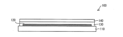
- FIG. 5 is a cross-sectional view illustrating a schematic configuration of the organic EL display device.
- the organic EL display device 100 includes a TFT (thin film transistor) substrate 110, an organic EL element 120, an adhesive layer 130, and a sealing substrate 140.
- TFT thin film transistor
- a TFT or the like is formed as a switching element in a portion that becomes a pixel region.
- the organic EL element 120 is formed in a matrix in the display area of the TFT substrate 110.
- the TFT substrate 110 on which the organic EL element 120 is formed is bonded to the sealing substrate 140 with an adhesive layer 130 or the like.
- FIG. 6 is a cross-sectional view showing a schematic configuration of the organic EL element 120 constituting the display unit of the organic EL display device 100.
- the TFT substrate 110 has a configuration in which a TFT 112 (switching element) and wiring 113, an interlayer insulating film 114, an edge cover 115, and the like are formed on a transparent insulating substrate 111 such as a glass substrate. ing.
- the organic EL display device 100 is a full-color active matrix organic EL display device.
- red (R), green (G), blue On the insulating substrate 111, red (R), green (G), blue ( The pixels 101R, 101G, and 101B of the respective colors including the organic EL elements 120 of the respective colors B) are arranged in a matrix.
- the TFTs 112 are provided corresponding to the pixels 101R, 101G, and 101B, respectively.
- the structure of the TFT is well known from the past. Therefore, illustration and description of each layer in the TFT 112 are omitted.
- the interlayer insulating film 114 is laminated over the entire area of the insulating substrate 111 on the insulating substrate 111 so as to cover each TFT 112 and the wiring 113.
- the first electrode 121 in the organic EL element 120 is formed on the interlayer insulating film 114.
- the interlayer insulating film 114 is provided with a contact hole 114a for electrically connecting the first electrode 121 in the organic EL element 120 to the TFT 112. Thereby, the TFT 112 is electrically connected to the organic EL element 120 through the contact hole 114a.
- the edge cover 115 prevents the first electrode 121 and the second electrode 126 in the organic EL element 120 from being short-circuited when the organic EL layer becomes thin or the electric field concentration occurs at the end of the first electrode 121.
- This is an insulating layer.
- the edge cover 115 is formed on the interlayer insulating film 114 so as to cover the end portion of the first electrode 121.
- the first electrode 121 is exposed at a portion where the edge cover 115 is not provided. This exposed portion becomes a light emitting portion of each of the pixels 101R, 101G, and 101B.
- each of the pixels 101R, 101G, and 101B is partitioned by the edge cover 115 having an insulating property.
- the edge cover 115 also functions as an element isolation film.
- insulating substrate 111 for example, alkali-free glass, plastic, or the like can be used. In the present embodiment, alkali-free glass having a thickness of 0.7 mm is used.
- the interlayer insulating film 114 and the edge cover 115 a known photosensitive resin can be used.
- the photosensitive resin include acrylic resin and polyimide resin.
- the TFT 112 is manufactured by a known method.
- the active matrix organic EL display device 100 in which the TFT 112 is formed in each of the pixels 101R, 101G, and 101B is taken as an example.
- the present embodiment is not limited to this, and the present invention can also be applied to the manufacture of a passive matrix organic EL display device in which TFTs are not formed.
- the organic EL element 120 is a light emitting element that can emit light with high luminance by low voltage direct current drive, and a first electrode 121, an organic EL layer, and a second electrode 126 are laminated in this order.
- the first electrode 121 is a layer having a function of injecting (supplying) holes into the organic EL layer. As described above, the first electrode 121 is connected to the TFT 112 through the contact hole 114a.
- a hole injection layer / hole transport layer 122 for example, from the first electrode 121 side, for example, a hole injection layer / hole transport layer 122, a light emitting layer 123R. 123G * 123B, the electron carrying layer 124, and the electron injection layer 125 have the structure formed in this order.
- a carrier blocking layer for blocking the flow of carriers such as holes and electrons may be inserted as necessary.
- One layer may have a plurality of functions. For example, one layer serving as both a hole injection layer and a hole transport layer may be formed.
- the stacking order is that in which the first electrode 121 is an anode and the second electrode 126 is a cathode.
- the order of stacking the organic EL layers is reversed.
- the hole injection layer is a layer having a function of increasing the hole injection efficiency into the light emitting layers 123R, 123G, and 123B.
- the hole transport layer is a layer having a function of improving the efficiency of transporting holes to the light emitting layers 123R, 123G, and 123B.
- the hole injection / hole transport layer 122 is uniformly formed on the entire display region of the TFT substrate 110 so as to cover the first electrode 121 and the edge cover 115.
- the hole injection layer / hole transport layer 122 in which the hole injection layer and the hole transport layer are integrated is provided as the hole injection layer and the hole transport layer. ing.
- this embodiment is not limited to this, and the hole injection layer and the hole transport layer may be formed as independent layers.
- light emitting layers 123R, 123G, and 123B are formed corresponding to the pixels 101R, 101G, and 101B, respectively.
- the light emitting layers 123R, 123G, and 123B are layers having a function of emitting light by recombining holes injected from the first electrode 121 side and electrons injected from the second electrode 126 side.
- the light emitting layers 123R, 123G, and 123B are each formed of a material having high light emission efficiency, such as a low molecular fluorescent dye or a metal complex.
- the electron transport layer 124 is a layer having a function of increasing the electron transport efficiency from the second electrode 126 to the light emitting layers 123R, 123G, and 123B.
- the electron injection layer 125 is a layer having a function of increasing the electron injection efficiency from the second electrode 126 to the light emitting layers 123R, 123G, and 123B.
- the electron transport layer 124 is formed on the light emitting layer 123R / 123G / 123B and the hole injection layer / hole transport layer 122 so as to cover the light emitting layer 123R / 123G / 123B and the hole injection layer / hole transport layer 122.
- the TFT substrate 110 is uniformly formed over the entire display area.
- the electron injection layer 125 is uniformly formed on the entire surface of the display region of the TFT substrate 110 on the electron transport layer 124 so as to cover the electron transport layer 124.
- the electron transport layer 124 and the electron injection layer 125 may be formed as independent layers as described above, or may be provided integrally with each other. That is, the organic EL display device 100 may include an electron transport layer / electron injection layer instead of the electron transport layer 124 and the electron injection layer 125.
- the second electrode 126 is a layer having a function of injecting electrons into the organic EL layer composed of the organic layers as described above.
- the second electrode 126 is uniformly formed on the electron injection layer 125 over the entire display region of the TFT substrate 110 so as to cover the electron injection layer 125.
- organic layers other than the light-emitting layers 123R, 123G, and 123B are not essential layers as the organic EL layer, and may be appropriately formed according to the required characteristics of the organic EL element 120.
- one layer may have a plurality of functions.
- a carrier blocking layer can be added to the organic EL layer as necessary. For example, by adding a hole blocking layer as a carrier blocking layer between the light emitting layers 123R, 123G, and 123B and the electron transport layer 124, holes are prevented from passing through the electron transport layer 124, thereby improving luminous efficiency. can do.
- the first electrode 121 is formed in a pattern corresponding to each of the pixels 101R, 101G, and 101B by photolithography and etching after an electrode material is formed by sputtering or the like.
- the first electrode 121 in the case of a bottom emission type organic EL element that emits light to the insulating substrate 111 side, it is necessary to be transparent or translucent.
- the second electrode 126 needs to be transparent or translucent.
- Examples of conductive film materials used for the first electrode 121 and the second electrode 126 include ITO (Indium Tin Oxide), IZO (Indium Zinc Oxide), gallium-doped zinc oxide (A transparent conductive material such as GZO) or a metal material such as gold (Au), nickel (Ni), or platinum (Pt) can be used.
- ITO Indium Tin Oxide
- IZO Indium Zinc Oxide
- GZO gallium-doped zinc oxide
- a transparent conductive material such as GZO
- a metal material such as gold (Au), nickel (Ni), or platinum (Pt) can be used.
- a sputtering method a vacuum deposition method, a CVD (chemical vapor deposition) method, a plasma CVD method, a printing method, or the like can be used.
- a sputtering method a vacuum deposition method
- a CVD (chemical vapor deposition) method a plasma CVD method, a printing method, or the like.
- stacking of the said 1st electrode 121 As shown in FIG.
- Each of the light emitting layers 123R, 123G, and 123B may be made of a single material, or may be a mixed material in which a certain material is used as a host material and another material is mixed as a guest material or a dopant. .
- Examples of the material of the hole injection layer, the hole transport layer, or the hole injection layer / hole transport layer 122 include anthracene, azatriphenylene, fluorenone, hydrazone, stilbene, triphenylene, benzine, styrylamine, triphenylamine, and porphyrin. , Triazoles, imidazoles, oxadiazoles, oxazoles, polyarylalkanes, phenylenediamines, arylamines, and derivatives thereof, polysilane compounds, thiophene compounds, vinylcarbazole compounds, aniline compounds, etc. A monomer, an oligomer, a polymer, etc. are mentioned.
- a material having high luminous efficiency such as a low molecular fluorescent dye or a metal complex is used.
- a material having high luminous efficiency such as a low molecular fluorescent dye or a metal complex.
- Examples of the material for the electron transport layer 124, the electron injection layer 125, or the electron transport layer / electron injection layer include tris (8-quinolinolato) aluminum complex, oxadiazole derivative, triazole derivative, phenylquinoxaline derivative, silole derivative, and the like. Can be mentioned.
- FIG. 7 is a cross-sectional view showing a schematic configuration of a conventional vacuum vapor deposition apparatus 90.
- the vacuum deposition apparatus 90 includes a vacuum chamber 10 as a film forming chamber.
- various components such as a vapor deposition source 20, a deposition plate 30, and a shutter 40 are provided.
- the vacuum chamber 10 has a vacuum pump (not shown) that evacuates the vacuum chamber 10 through an exhaust port (not shown) provided in the vacuum chamber 10 in order to keep the vacuum chamber 10 in a vacuum state during vapor deposition. Etc. are provided.
- the vacuum chamber 10 can be depressurized by a vacuum pump (not shown) or the like, and has an opening / closing portion, and is capable of attaching, removing, taking in and out various components provided in the vacuum chamber 10 so as to be detachable. Is possible.
- the vapor deposition source 20 injects a vapor deposition material such as an organic light emitting material as vapor deposition particles by heating and sublimating the vapor deposition material, which is a film forming material, under high vacuum.
- a vapor deposition material such as an organic light emitting material as vapor deposition particles by heating and sublimating the vapor deposition material, which is a film forming material, under high vacuum.
- the vapor deposition source 20 includes, for example, a container called “crucible” or “boat” as a vapor deposition material storage (not shown) that stores the vapor deposition material therein.
- the injection of the sublimated vapor deposition particles may be performed directly from the vapor deposition material storage unit, may have a load lock type pipe, and may be injected through the load lock type pipe.
- a vapor deposition mask 50 called a shadow mask in which an opening 51 (through hole, see FIG. 8) is formed at a desired position and shape is used.
- the vapor deposition source 20 is disposed opposite to the mask 50 disposed in the vacuum chamber 10 with a certain gap (that is, separated by a certain distance). Further, the vapor deposition source 20 is disposed so as to face the film formation surface 61 of the film formation substrate 60 through the mask 50 disposed in the vacuum chamber 10.
- the vapor deposition source 20 has an injection port 21 on the surface facing the mask 50 for injecting (scattering) the vapor deposition material as vapor deposition particles. Moreover, the vapor deposition source 20 shown in FIG. 7 has a mechanism which injects vapor deposition particles upwards, for example.
- the deposition source 20 is disposed below the film formation substrate 60, and the film formation substrate 60 is held in close contact with the mask 50 with the film formation surface 61 facing downward. This is illustrated with an example of the case.
- a deposition plate 30 is disposed in a scattering region of the deposition particles that are not desired to be deposited (an extra scattering region other than the injection path, which is a necessary scattering region of the deposition particles). Is provided.
- a first deposition plate 31 and a second deposition plate 32 are provided as the deposition plate 30.
- the vapor deposition particle injection path connecting the injection port 21 of the vapor deposition source 20 and the opening region (opening group forming region) in the mask 50, which becomes a vapor flow discharge port, is excluded.
- a first deposition plate 31 having an opening 31 a serving as the vapor flow outlet is provided adjacent to the inner wall 11 of the vacuum chamber 10 so as to cover the inner wall 11 of the vacuum chamber 10.
- a second deposition plate 32 having an opening 32a serving as the vapor flow outlet is provided around the vapor deposition source 20 so as to surround the vapor deposition source 20 except for the injection path.
- vapor deposition particles are present on the inner wall 11 of the vacuum chamber 10, each member or the like (for example, a drive unit) disposed in the vacuum chamber 10, and an extra portion other than the opening area of the mask 50.
- the deposition preventing plate 30 is provided as described above.
- a shutter 40 is provided for determining whether or not.
- the shutter 40 prevents vapor deposition particles from being ejected into the vacuum chamber 10 when the vapor deposition rate is stabilized or when vapor deposition is unnecessary. For example, during the alignment of the film formation substrate 60 and the mask 50, the injection path of the vapor deposition particles is prevented so that the vapor deposition particles do not reach the film formation substrate 60.
- the shutter 40 is provided between the mask 50 and the vapor deposition source 20 so as to be capable of moving back and forth (insertable), for example.
- the shutter 40 closes the opening 51 of the mask 50 by being inserted between the mask 50 and the vapor deposition source 20 based on, for example, a vapor deposition OFF signal from a control unit (not shown).
- the opening 51 of the mask 50 is opened by being separated from between the mask 50 and the vapor deposition source 20 based on a vapor deposition ON signal from a control unit (not shown).
- the components (members) disposed in the vacuum chamber 10 such as the deposition plate 30 and the shutter 40 and provided at positions where the deposition material such as the organic EL material, which is a film deposition material to be collected, is attached. It can be attached and detached for the purpose of reducing the cleaning work of the vapor deposition material adhering to the structure.
- the anti-adhesion plate 30 may be formed by bending a thin plate-like base material, but is preferably divided and installed so that it can be easily attached and detached.
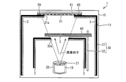
- FIG. 1 is a cross-sectional view showing a schematic configuration of a vacuum vapor deposition apparatus 1 in which a layer 3 made of a refractory material is provided on a surface of a chamber component on which the vapor deposition particles are deposited.
- the vacuum vapor deposition apparatus 1 is a vacuum vapor deposition apparatus 1 in a vacuum chamber 10 such as the above-mentioned deposition preventing plate 30, shutter 40, mask 50, etc. used as a film forming jig.
- a vacuum chamber 10 such as the above-mentioned deposition preventing plate 30, shutter 40, mask 50, etc. used as a film forming jig.
- the in-chamber component provided at the position where the vapor deposition material adheres as described above 7 is different from the conventional vacuum vapor deposition apparatus 90 shown in FIG. 7 in that at least a part of the surface on which the vapor deposition particles are vapor deposited is formed of a high melting point material.
- the high melting point material means that the vapor deposition material storage unit (not shown) provided in the vapor deposition source 20 does not decompose the vapor deposition material stored in the vapor deposition material storage unit and can obtain a predetermined vapor deposition rate.
- the material is set so as to be in a temperature region (deposition temperature region), but does not have a melting point and a sublimation point below the maximum temperature in the temperature region.
- the in-chamber component has a layer made of a high melting point material on at least the surface on the side where the vapor deposition particles are deposited.
- these chamber components may be entirely composed of a high melting point material, or only the surface thereof may be composed of a high melting point material.
- the entire surface on the side on which the deposited particles are deposited is composed of a high melting point material, but the present invention is not limited to this.
- the structure only a part with a large amount of vapor deposition particles may be composed of a high melting point material.
- a layer 3 made of a high melting point material is provided on the surface of the deposition preventing plate 30 or the shutter 40 on the side where the vapor deposition particles are vapor deposited.
- the layer 3 made of a high-melting-point material is formed of alumina having a melting point of about 2000 ° C. at normal pressure.
- the layer 3 is not limited to this, and varies depending on the type. Generally, glass having a melting point of 600 ° C. to 700 ° C. at normal pressure or silicon carbide having a melting point of 2700 ° C. at normal pressure can be used.
- the layer 3 made of a high melting point material is formed by using one material selected from iron, cobalt, nickel and stainless steel, or a material made of an alloy of two or more materials selected from the above. It may be formed.
- the above-described organic material is not decomposed and deposition is performed so as to obtain a predetermined deposition rate.
- the temperature region is generally 200 ° C. to 400 ° C., and the vapor deposition material container 19 is appropriately set within this temperature region.
- FIG. 2 shows a process of recovering the vapor deposition film 4 attached on the layer 3 made of a high melting point material provided on the deposition preventing plate 30 or the shutter 40 of the vacuum vapor deposition apparatus 1 and reusing it in the vacuum vapor deposition apparatus 1 (deposition). It is a figure for demonstrating the collection
- the deposited film 4 deposited on the layer 3 made of a high melting point material provided on the adhesion preventing plate 30 or the shutter 40 is scraped by using a spatula 2 called a scraper as a cutting tool. Shows how to drop.
- the spatula 2 is used as the cutting tool, but the present invention is not limited to this, and a grinder, a polisher, or the like can be used as the cutting tool.
- Embodiment 2 Furthermore, a sand blast method using an abrasive described in Embodiment 2 may be used.
- the hardness of the spatula 2 used as a cutting tool is higher than that of alumina which is the layer 3 made of a high melting point material.
- the material collected by scraping is pulverized, and again in the vapor deposition material storage section 19 which is a container called “crucible” or “boat” as the vapor deposition material. It is thrown.
- the vapor deposition material container 19 is placed in the vapor deposition source 20 of the vacuum vapor deposition apparatus 1 shown in FIG. Heated.
- the materials charged in the vapor deposition material storage unit 19 are alumina and the vapor deposition film 4, even if the temperature of the vapor deposition material storage unit 19 is increased to 200 ° C. to 400 ° C., which is the vapor deposition temperature region of the vapor deposition film 4,
- the vapor deposition material can be reused without deteriorating the vapor deposition material.
- alumina does not react with the vapor deposition film 4 as the vapor deposition material, and the vapor deposition material is not denatured.
- the layer 3 made of the high melting point material it is preferable to use a material that does not react with the vapor deposition material even if the temperature of the vapor deposition material storage portion 19 is raised to the vapor deposition temperature region.
- the vacuum deposition apparatus 1 and the spatula 2 having a hardness higher than that of alumina, which is the layer 3 made of a high melting point material the deposited film 4 attached to the deposition preventing plate 30 and the shutter 40 is recovered and complicated. Therefore, it can be reused without any separation or purification treatment.
- it is a method of immersing a composition having a deposition material attached thereto in an organic solvent.
- a method of immersing a composition having a deposition material attached thereto in an organic solvent By using such a method, only the vapor deposition material can be dissolved and separated in an organic solvent.
- the hardness of the layer 3 made of the high melting point material is not particularly limited, but the number of times of use decreases when it is desorbed or modified in large quantities by the deposit peeling process. It is better to have hardness.
- the layer 3 made of the high melting point material should have as high a hardness as possible from the viewpoint of reducing the amount of the desorbed material.
- the material to be used may be appropriately adjusted in consideration of the workability and material cost of the high melting point material.
- the material collected by scraping which is the step shown in FIG. 2C, is pulverized and put into the vapor deposition material storage unit 19, it may be filtered.
- the high melting point material is accumulated in the vapor deposition material storage unit 19. This means that the high melting point material can be recovered after a certain amount, and the present invention also has an effect of reusing the high melting point material.
- the high melting point material is expensive, the cost can be reduced by collection and reuse. If the high melting point material is an environmental pollutant, it is useful for environmental conservation by reducing waste.
- the material collected by scraping is reused in the vacuum vapor deposition apparatus 1 shown in FIG. 1 in consideration of repeated collection and reuse multiple times. Even if the conventional vacuum deposition apparatus 90 is used, it can be reused.
- the in-chamber component (an adhesion preventing member) in the present embodiment is provided between the substrate and the opening through which the vapor deposition particles are discharged from the vapor deposition material storage unit, and is normal to the substrate. It is formed at predetermined intervals along the direction perpendicular to the direction so that the opening is sandwiched between them, the maximum incident angle of the vapor deposition particles to the substrate is reduced, and blurring generated at the edge of the film formed on the substrate is suppressed.
- a plurality of control plates that can be used or a combination of these control plates may be included.
- FIG. 8 is a cross-sectional view schematically showing a method of forming a film formation pattern on a film formation substrate by a vacuum evaporation method.
- the TFT substrate 110 is used as the film formation substrate 60, an organic light emitting material is used as the vapor deposition material, and the vacuum evaporation method is formed on the film formation substrate 60 on which the first electrode 121 is formed.
- an organic EL layer is formed as a vapor deposition film will be described as an example.
- the illustration of the in-chamber components 70 other than the mask 50 such as the deposition preventing plate 30 and the shutter 40 is omitted.
- the pixels 101R, 101G, and 101B are arranged in a matrix.
- each color of, for example, cyan (C), magenta (M), and yellow (Y) is used. You may have a light emitting layer, and you may have the light emitting layer of each color which consists of red (R), green (G), blue (B), and yellow (Y).
- a color image display is performed by selectively emitting light of these organic EL elements 120 with a desired luminance using the TFT 112.
- the organic EL display device 100 it is necessary to form a light emitting layer made of an organic light emitting material that emits light of each color in a predetermined pattern on the film formation substrate 60 for each organic EL element 120. There is.
- the vapor deposition mask 50 is formed with the opening 51 at a desired position and shape.
- the mask 50 is disposed opposite to the film formation surface 61 of the film formation substrate 60 via a fixed or fixed gap.
- the mask 50 has the same size as the film formation substrate 60 and is tightly fixed to the film formation surface 61 of the film formation substrate 60. Is not limited to this.
- the mask 50 having a size smaller than that of the deposition target substrate 60 is used, and the deposition target substrate 60 is moved along the injection path of the vapor deposition particles emitted from the deposition source 20 with the mask 50 and the deposition source 20 fixed. You may move so that it may pass.
- the vapor deposition method itself is not particularly important as long as at least the surface of the in-chamber component 70 is formed of a high melting point material. Therefore, the present invention can be applied even when different vapor deposition methods are used as described above.
- the vapor deposition source 20 is disposed on the opposite side of the deposition target substrate 60 across the mask 50 so as to face the deposition target surface 61 of the deposition target substrate 60. Is done.
- the organic light emitting material is ejected from the vapor deposition source 20 as vapor deposition particles by being heated and sublimated under high vacuum.
- the vapor deposition material injected from the vapor deposition source 20 as vapor deposition particles is vapor deposited on the film formation substrate 60 through the opening 51 provided in the mask 50.
- an organic film having a desired film formation pattern is vapor-deposited as a vapor deposition film only at a desired position of the film formation substrate 60 corresponding to the opening 51.
- vapor deposition is performed for every color of a light emitting layer (this is called "separate vapor deposition").
- an open mask having an opening only on the entire surface of the display portion and an area where film formation is required is used. To form a film.
- the electron transport layer 124 the electron injection layer 125, and the second electrode 126.
- the film when forming the light emitting layer 123 ⁇ / b> R of the pixel displaying red, the film is formed using the fine mask having an opening only in the region where the red light emitting material is deposited as the deposition mask 50. .
- FIG. 9 is a flowchart showing manufacturing steps of the organic EL display device 100 in the order of steps.
- the TFT substrate 110 is fabricated, and the first electrode 121 is formed on the fabricated TFT substrate 110 (step S1).
- the TFT substrate 110 can be manufactured using a known technique.
- the hole injection layer and the hole transport layer are formed on the entire surface of the pixel region by vacuum evaporation using an open mask as the evaporation mask 50.
- the hole injection layer and the hole transport layer can be the hole injection layer / hole transport layer 122 as described above.
- step S3 the light emitting layers 123R, 123G, and 123B are separately deposited by vacuum vapor deposition. Thereby, a pattern film corresponding to each of the pixels 101R, 101G, and 101B is formed.
- the electron transport layer 124, the electron injection layer 125, and the second electrode 126 are sequentially vacuumed on the TFT substrate 110 on which the light emitting layers 123R, 123G, and 123B are formed, using an open mask as a vapor deposition mask 50. It is formed over the entire pixel region by vapor deposition (steps S4 to S6).
- the region (display unit) of the organic EL element 120 is sealed so that the organic EL element 120 is not deteriorated by moisture or oxygen in the atmosphere with respect to the substrate on which the vapor deposition is completed (step S7). ).
- Sealing includes a method of forming a film that does not easily transmit moisture or oxygen by a CVD method or the like, and a method of bonding a glass substrate or the like with an adhesive or the like.
- the organic EL display device 100 is manufactured through the processes as described above.
- the organic EL display device 100 can perform desired display by causing a current to flow from the driving circuit formed outside to the organic EL element 120 in each pixel to emit light.
- a second embodiment of the present invention will be described based on FIG.
- a sandblasting method using a spraying tool 5a and a polishing agent 5b made of a high melting point material as a shaving tool is applied to the deposition preventing plate 30 and the shutter 40 that are not provided with a high melting point material.
- the second embodiment is different from the first embodiment in that the deposited vapor deposition film 4 is peeled off, and the other configuration is as described in the first embodiment.
- members having the same functions as those shown in the drawings of the first embodiment are given the same reference numerals, and descriptions thereof are omitted.
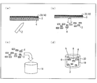
- FIG. 3 is a diagram for explaining a process of collecting the deposition film 4 attached to the deposition preventing plate 30 and the shutter 40 on which the high melting point material is not provided by the sandblasting method and reusing it in the vacuum deposition apparatus 1. .
- FIG. 3 (a) shows a deposited film attached to the deposition preventing plate 30 and the shutter 40, which is not provided with a high melting point material, by a sandblasting method using a spraying tool 5a and an abrasive 5b as a cutting tool. A state where 4 is scraped off is shown.
- the sand blasting method is a method in which an abrasive such as sand is sprayed on the surface to excavate or polish the surface.
- the abrasive 5b made of alumina is used as a cutting tool, and the hardness of alumina is lower than the material constituting the deposition preventing plate 30 and the shutter 40.
- the collected material in which the abrasive 5 b and the vapor deposition material (deposition film 4) are mixed is pulverized and put into the vapor deposition material storage unit 19 as it is.
- the vapor deposition material container 19 is placed in the vapor deposition source 20 of the vacuum vapor deposition apparatus 1 shown in FIG. Heated.
- the temperature of the vapor deposition material storage unit 19 is set to 200 ° C. or higher, which is the vapor deposition temperature region of the vapor deposition material. Even when the temperature is raised to 400 ° C., the vapor deposition material can be reused without deteriorating the vapor deposition material.
- the material collected by scraping is reused in the vacuum vapor deposition apparatus 1 shown in FIG. 1 in consideration of repeated collection and reuse multiple times. Even if the conventional vacuum deposition apparatus 90 is used, it can be reused.
- an organic solvent is not used, and a sand blasting method that can efficiently and sufficiently desorb deposits from the surface of the component is used.
- a scraper, grinder Polishers can also be used.
- the portion in contact with the deposit must be made of a high melting point material, and the hardness of the high melting point material is:
- the material needs to be lower than the material constituting the deposition preventing plate 30 and the shutter 40.
- the deposition film 4 attached on the layer 3 made of a high melting point material provided on the deposition preventing plate 30 or the shutter 40 is used as a cutting tool, and at least a portion in contact with the deposition film 4 is high.
- the second embodiment is different from the first and second embodiments in that peeling is performed using a spatula 2a made of a melting point material, and the other configuration is as described in the first embodiment.
- members having the same functions as those shown in the drawings of Embodiments 1 and 2 are given the same reference numerals, and descriptions thereof are omitted.
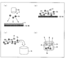
- FIG. 4 shows that the deposition film 4 attached on the layer 3 made of a high melting point material provided on the deposition preventing plate 30 or the shutter 40 has a spatula 2a made of a high melting point material at least in contact with the deposition film 4. It is a figure for demonstrating the process collect
- FIG. 4 shows that the deposition film 4 attached on the layer 3 made of a high melting point material provided on the deposition preventing plate 30 or the shutter 40 has a spatula 2a made of a high melting point material at least in contact with the deposition film 4.
- FIG. 4A shows a high melting point provided on the deposition preventing plate 30 and the shutter 40 using a spatula 2a made of alumina, which is a high melting point material, at least in contact with the vapor deposition film 4 as a cutting tool.
- a spatula 2a made of alumina which is a high melting point material
- the deposition preventing plate 30 and the shutter 40 are provided with a layer 3 (alumina) made of a high melting point material, and the spatula 2a as a cutting tool also has a portion in contact with the vapor deposition film 4. It is composed of a high melting point material (alumina).
- the vapor deposition material container 19 is placed in the vapor deposition source 20 of the vacuum vapor deposition apparatus 1 shown in FIG. Heated.
- the high melting point material used in the spatula 2a and the high melting point material used in the deposition preventing plate 30 and the shutter 40 are used from the viewpoint of reusing the high melting point material accumulated in the vapor deposition material storage unit 19.
- At least a part of the surface on which the deposited particles are deposited is made of a material that does not react with the deposited material at the maximum temperature or lower in the temperature range.
- the vapor deposition material is an organic material, and the temperature range is preferably 200 degrees or more and 400 degrees or less.
- the surface on which the vapor deposition particles are vapor-deposited is made of one material selected from alumina, glass, and silicon carbide.
- At least a part of the surface on which the deposited particles are deposited is at least one material selected from iron, cobalt, nickel, and stainless steel, or from the above It is preferably made of an alloy of two or more selected materials.
- the deposition member includes a deposition plate for preventing the deposition chamber from being contaminated by the deposited particles.
- the adhesion preventing member has a shutter for preventing vapor deposition particles released from the vapor deposition material storage portion from being vapor deposited on the substrate during the second period. It is preferably included.
- the adhesion preventing member is provided between an opening through which the vapor deposition particles are discharged from the vapor deposition material storage unit and the substrate, and is perpendicular to the normal direction of the substrate. It is preferable that a plurality of control plates formed at a predetermined interval so as to sandwich the opening portion or a combination of the plurality of control plates is included.
- the deposition member includes a deposition plate, a shutter, and a control plate with a relatively large deposition amount of vapor deposition particles, a vapor deposition apparatus that can efficiently collect the vapor deposition material can be realized.
- At least a portion in contact with the deposited film deposited on the surface of the deposition preventing member is made of a material that does not react with the deposited material at the maximum temperature or lower in the temperature range.
- the vapor deposition material stored in the vapor deposition material storage unit is an organic material, and the temperature range is 200 degrees or more and 400 degrees or less.
- At least a portion in contact with the deposited film deposited on the surface of the deposition preventing member is made of one material selected from alumina, glass, and silicon carbide.
- At least a portion in contact with the deposited film deposited on the surface of the adhesion-preventing member is selected from one material selected from iron, cobalt, nickel and stainless steel, or from the above.
- it is made of an alloy of two or more materials.
- At least a portion in contact with the deposited film deposited on the surface of the deposition preventing member has a hardness lower than that of the deposition preventing member.
- the abrasive is brought into contact with the deposited film deposited on the surface of the deposition member of the deposition apparatus to peel off the deposited film.
- the material for constituting at least a part of the surface on which the vapor deposition particles are vapor-deposited in the adhesion member and the tool are vapor-deposited at least on the surface of the adhesion member. It is preferable that the portion in contact with the deposited film is formed of the same material.
- the material constituting the portion to be made is the same material, there is no need to separate it separately, so that it can be reused efficiently.
- the adhesion preventing member is divided and provided.
- the deposition preventing member is divided and easy to attach and detach, so that it is easy to collect the vapor deposition material deposited on the deposition preventing member.
- the present invention can be applied to a vapor deposition apparatus and a cutting tool for recovering vapor deposition material deposited on unnecessary portions.
- Vacuum deposition equipment 1,90 Vacuum deposition equipment (vapor deposition equipment) 2, 2a Spatula (cutting tool) 3 Layer made of high melting point material 4 Deposition film 5 Cutting tool 5a Spraying tool 5b Abrasive agent 10 Vacuum chamber (deposition chamber) DESCRIPTION OF SYMBOLS 11 Inner wall 19 Vapor deposition material storage part 20 Vapor deposition source 21 Injection port 30 Prevention plate (attachment prevention member) 31 1st deposition board (protection member) 31a opening 32 2nd adhesion prevention board (attachment prevention member) 32a Opening 40 Shutter (proofing member) 50 Mask 51 Opening 60 Deposition Substrate 61 Deposition Surface
Landscapes
- Chemical & Material Sciences (AREA)
- Chemical Kinetics & Catalysis (AREA)
- Engineering & Computer Science (AREA)
- Materials Engineering (AREA)
- Mechanical Engineering (AREA)
- Metallurgy (AREA)
- Organic Chemistry (AREA)
- Electroluminescent Light Sources (AREA)
Abstract
真空チャンバ(10)において、蒸着材料収納部(19)は、蒸着材料収納部(19)に収納されている蒸着材料が分解せず、かつ、所定の蒸着速度を得られる温度領域となるように設定され、蒸着材料収納部(19)から第1の期間中、第1の方向に放出される蒸着粒子は、基板(60)上に蒸着され、蒸着材料収納部(19)から上記第1の期間中、上記第1の方向とは異なる第2の方向に放出される蒸着粒子または、上記第1の期間とは異なる第2の期間中、蒸着材料収納部(19)から放出される蒸着粒子は、真空蒸着装置1から取り外しできる防着板(30)やシャッタ(40)に蒸着され、防着板(30)やシャッタ(40)において、少なくとも上記蒸着粒子が蒸着される面には、上記温度領域における最高温度以下においては、融点および昇華点を有さない材料からなる層(3)が設けられている。
Description
本発明は、不要な部分に蒸着された蒸着材料を回収するための蒸着装置、削具および蒸着材料の回収方法に関するものである。
近年、大量生産・大量廃棄の社会へと変貌を遂げる中、電子機器、特に情報関連機器の増加は顕著である。上記電子機器の中核部品としては、半導体、液晶パネルを含むフラットディスプレイパネル、太陽電池、半導体デバイス、メモリ等が挙げられる。
このような電子機器は、スパッタリング法、真空蒸着法、イオンプレーティング法等の真空成膜法による真空成膜装置を用いて作製されており、成膜材に希少金属が用いられることも多い。
また、近年、様々な商品や分野でフラットパネルディスプレイが活用されており、フラットパネルディスプレイのさらなる大型化、高画質化、低消費電力化が求められている。
そのような状況下において、有機材料の電界発光(エレクトロルミネッセンス;以下、「EL」と記す)を利用した有機EL素子を備えた有機EL表示装置は、全固体型で、低電圧駆動、高速応答性、自発光性等の点で優れたフラットパネルディスプレイとして、高い注目を浴びている。
有機EL表示装置は、例えば、TFT(薄膜トランジスタ)が設けられたガラス基板等からなる基板上に、TFTに接続された有機EL素子が設けられた構成を有している。
有機EL素子は、低電圧直流駆動による高輝度発光が可能な発光素子であり、第1電極、有機EL層、および第2電極が、この順に積層された構造を有している。そのうち、第1電極はTFTと接続されている。
また、第1電極と第2電極との間には、上記有機EL層として、正孔注入層、正孔輸送層、電子ブロッキング層、発光層、正孔ブロッキング層、電子輸送層、電子注入層等を積層させた有機層が設けられている。
フルカラーの有機EL表示装置は、一般的に、赤(R)、緑(G)、青(B)の各色の有機EL素子をサブ画素として基板上に配列形成してなり、TFTを用いて、これら有機EL素子を選択的に所望の輝度で発光させることにより画像表示を行っている。
このような有機EL表示装置の発光部における有機EL素子は、一般的に、有機膜の積層蒸着によって形成される。有機EL表示装置の製造においては、少なくとも各色に発光する有機発光材料からなる発光層が、発光素子である有機EL素子毎に所定のパターンで成膜される。
積層蒸着による所定のパターンの成膜には、例えば、「シャドウマスク」と称される蒸着用のマスクを用いた真空蒸着法、インクジェット法、レーザ転写法等が適用可能である。
そのうち、現在では真空蒸着法を用いるのが最も一般的である。
真空蒸着法では、蒸着源に備えられ、内部に蒸着材料を収容する蒸着材料収納部である「るつぼ」あるいは「ボート」と称されるものを使用し、高真空下で上記蒸着材料を加熱して昇華させることにより、被成膜基板上に上記蒸着材料を蒸着させる。
このとき、蒸着粒子として上記蒸着材料収納部から射出された蒸着材料を、真空蒸着装置における真空チャンバ内で、上記蒸着用のマスクに設けられた開口部を通して蒸着させることで、所望の成膜パターンを得ることができる。
有機EL表示装置の発光部における有機EL素子は、有機膜の積層蒸着によって構成されている。
真空蒸着法では、上記したように蒸着材料を加熱し昇華させて蒸着粒子として蒸着源から射出されるため、飛散した蒸着粒子は、TFT基板等の被成膜基板以外の構成物にも付着する。
真空蒸着装置における真空チャンバ内には、防着板やシャッタ等、様々な構成物がある。
上記有機膜を構成する有機材料は高価であるが、これらの構成物に付着した蒸着材料、すなわちTFT基板等の被成膜基板以外に付着した蒸着粒子は、回収されない限り全て無駄となる。
現状、有機EL表示装置の量産で適用されている製造装置では、真空チャンバ内の防着板等に付着した有機材料は再利用できず、材料利用効率が低かった。
なお、材料利用効率とは、蒸着時に使用する材料のうち実際に活用される材料の比率を示す。
そこで、被成膜基板以外に付着した蒸着材料を回収し、再利用することができれば、材料利用効率が向上する。
そこで、例えば特許文献1には、セルシャッタに付着した蒸着材料を加熱して再蒸発させ、その蒸気を冷却媒体が循環されるシュラウドで冷却して回収する方法が開示されている。
また、特許文献2には、シャッタ板に付着した蒸着材料をシャッタ内のヒータにより加熱、融解させ蒸着源に落とし込んで回収する方法が開示されている。
特許文献3には、ヒータでセルシャッタを加熱し、セルシャッタの下面に付着した蒸着材料を蒸発させて坩堝(るつぼ)に回収する方法が開示されている。
特許文献4には、遮断壁と蒸気流放出口とを備えた蒸着材料回収具を、蒸気出口を覆うように配置し、蒸着源から被処理基板に向かう蒸気流の発散角が制御された状態で蒸着を行った後、上記蒸着材料回収具を取り出して遮断壁に堆積している蒸着材料を回収する方法が開示されている。
特許文献5には、有機材料が析出するチャンバ内におけるシャッタ等の部品を、有機材料が変質しない不活性な材質とし、これら部品に堆積した有機材料を回収することが開示されている。
特許文献6には、成膜治具への付着物をウォータジェットの吹き付けによって回収方法が開示されている。
しかしながら、特許文献1~3に記載の方法は、シャッタ以外の部分に付着した蒸着材料は回収し得ないという問題点を有している。
量産工程では、蒸着速度が安定した後、基板への蒸着処理を多数枚連続的に処理する。したがって、チャンバへの基板の出し入れや蒸着用のマスクの基板への密着期間という、僅かな時間を除いては、殆ど蒸着処理を行っており、シャッタは、殆どの期間、開放状態にあることになる。
このため、実際の量産工程では、シャッタ以外への蒸着材料の付着量が多く、シャッタに付着した蒸着材料を回収しただけでは、蒸着材料を効率的に回収、再利用することはできない。
しかも、蒸着材料の回収に際し加熱を行うことで、加熱による蒸着材料の劣化のおそれがある。
また、特許文献4に記載の方法では、遮断壁および被処理基板以外に付着した材料は回収が不可能であるという問題点を有している。
さらに、特許文献5には、チャンバ内におけるシャッタ等の部品に堆積した有機材料を回収することは開示されているものの、具体的な回収方法については開示がなされていない。
また、特許文献6に記載の方法は、水分により変性が生じ易い蒸着材料には適用することができない。しかも、水であっても、水圧により成膜治具の損傷、剥離があり、剥離した成膜治具は、剥離した蒸着材料に混入する。しかしながら、このように混入した不純物に関しては、言及がなされていない。
以上のように、従来の方法では、効率良く、且つ、低コストで成膜材料を回収することができなかった。
本発明は、上記の問題点に鑑みなされたものであり、その目的は、効率良く、且つ、低コストで蒸着材料を回収できる蒸着装置、削具および蒸着材料の回収方法を提供することにある。
本発明の蒸着装置は、上記の課題を解決するために、蒸着室において、蒸着源に備えられた蒸着材料収納部から放出された蒸着粒子を、基板上に蒸着させる蒸着装置であって、上記蒸着材料収納部の温度は、上記蒸着材料収納部に収納されている蒸着材料が分解せず、かつ、所定の蒸着速度を得られる温度領域となるように設定され、上記蒸着材料収納部から第1の期間中、第1の方向に放出される蒸着粒子は、上記基板上に蒸着され、上記蒸着材料収納部から上記第1の期間中、上記第1の方向とは異なる第2の方向に放出される蒸着粒子または、上記第1の期間とは異なる第2の期間中、上記蒸着材料収納部から放出される蒸着粒子は、上記蒸着装置から取り外しできる防着部材に蒸着され、上記防着部材において、少なくとも上記蒸着粒子が蒸着される面の少なくとも一部は、上記温度領域における最高温度以下においては、融点および昇華点を有さない材料からなることを特徴としている。
本発明の削具は、上記の課題を解決するために、上記蒸着装置に備えられた防着部材の表面に蒸着された蒸着膜を削って剥離でき、かつ、少なくとも、上記防着部材の表面に蒸着された蒸着膜と接触する部分は、上記防着部材より硬度が高いことを特徴としている。
上記構成によれば、上記防着部材において、少なくとも上記蒸着粒子が蒸着される面の少なくとも一部は、上記温度領域における最高温度以下においては、融点および昇華点を有さない材料からなるため、上記温度領域における最高温度以下においては、融点および昇華点を有さない材料より硬度が高い削具を用いて、上記蒸着装置に備えられた防着部材の表面に蒸着された蒸着膜を削って剥離する場合、上記温度領域における最高温度以下においては、融点および昇華点を有さない材料と蒸着材料のみを回収することができる。
したがって、上記温度領域における最高温度以下においては、融点および昇華点を有さない材料と蒸着材料のみからなる回収物をそのまま、上記蒸着材料収納部に入れて、再利用することができる。
よって、効率良く、且つ、低コストで蒸着材料を回収できる。
本発明の削具は、上記の課題を解決するために、蒸着室において、蒸着源に備えられた蒸着材料収納部から放出された蒸着粒子を、基板上に蒸着させる蒸着装置の防着部材の表面に蒸着された蒸着膜を削って剥離する削具であって、上記蒸着材料収納部の温度は、上記蒸着材料収納部に収納されている蒸着材料が分解せず、かつ、所定の蒸着速度を得られる温度領域となるように設定され、上記蒸着材料収納部から第1の期間中、第1の方向に放出される蒸着粒子は、上記基板上に蒸着され、上記蒸着材料収納部から上記第1の期間中、上記第1の方向とは異なる第2の方向に放出される蒸着粒子または、上記第1の期間とは異なる第2の期間中、上記蒸着材料収納部から放出される蒸着粒子は、上記蒸着装置から取り外しできる上記防着部材に蒸着され、上記削具において、少なくとも上記防着部材の表面に蒸着された蒸着膜と接触する部分は、上記温度領域における最高温度以下においては、融点および昇華点を有さない材料からなることを特徴としている。
本発明の蒸着材料の回収方法は、上記の課題を解決するために、請求項1から8の何れか1項に記載の蒸着装置と、請求項10から16の何れか1項に記載の削具とを、用いることを特徴としている。
上記方法によれば、上記防着部材において、少なくとも上記蒸着粒子が蒸着される面の少なくとも一部を構成する材料や上記削具において、上記防着部材の表面に蒸着された蒸着膜と接触する部分を構成する材料の硬度に関係なく、効率良く、且つ、低コストで蒸着材料を回収できる。
本発明の蒸着装置は、以上のように、上記蒸着材料収納部の温度は、上記蒸着材料収納部に収納されている蒸着材料が分解せず、かつ、所定の蒸着速度を得られる温度領域となるように設定され、上記蒸着材料収納部から第1の期間中、第1の方向に放出される蒸着粒子は、上記基板上に蒸着され、上記蒸着材料収納部から上記第1の期間中、上記第1の方向とは異なる第2の方向に放出される蒸着粒子または、上記第1の期間とは異なる第2の期間中、上記蒸着材料収納部から放出される蒸着粒子は、上記蒸着装置から取り外しできる防着部材に蒸着され、上記防着部材において、少なくとも上記蒸着粒子が蒸着される面の少なくとも一部は、上記温度領域における最高温度以下においては、融点および昇華点を有さない材料からなることを特徴としている構成である。
また、本発明の削具は、以上のように、請求項1から8の何れか1項に記載の蒸着装置に備えられた防着部材の表面に蒸着された蒸着膜を削って剥離でき、かつ、少なくとも、上記防着部材の表面に蒸着された蒸着膜と接触する部分は、上記防着部材より硬度が高いことを特徴としている構成である。
また、本発明の削具は、以上のように、上記蒸着材料収納部の温度は、上記蒸着材料収納部に収納されている蒸着材料が分解せず、かつ、所定の蒸着速度を得られる温度領域となるように設定され、上記蒸着材料収納部から第1の期間中、第1の方向に放出される蒸着粒子は、上記基板上に蒸着され、上記蒸着材料収納部から上記第1の期間中、上記第1の方向とは異なる第2の方向に放出される蒸着粒子または、上記第1の期間とは異なる第2の期間中、上記蒸着材料収納部から放出される蒸着粒子は、上記蒸着装置から取り外しできる上記防着部材に蒸着され、上記削具において、少なくとも上記防着部材の表面に蒸着された蒸着膜と接触する部分は、上記温度領域における最高温度以下においては、融点および昇華点を有さない材料からなる構成である。
また、本発明の蒸着材料の回収方法は、以上のように、請求項1から8の何れか1項に記載の蒸着装置と、請求項10から16の何れか1項に記載の削具とを、用いる方法である。
それゆえ、効率良く、且つ、低コストで蒸着材料を回収できる蒸着装置、削具および蒸着材料の回収方法を実現することができる。
以下、図面に基づいて本発明の実施の形態について詳しく説明する。ただし、この実施の形態に記載されている構成部品の寸法、材質、形状、その相対配置などはあくまで一実施形態に過ぎず、これらによってこの発明の範囲が限定解釈されるべきではない。
なお、以下の実施の形態においては、本発明の蒸着装置および削具が用いられる一例として、有機EL表示装置の製造工程に用いられる蒸着装置および削具を例に挙げて説明するが、これに限定されることはなく、本発明の蒸着装置および削具は、様々な分野の製造工程にて用いることができる。
〔実施の形態1〕
まず、図5および図6に基づいて、有機EL表示装置の構成について説明する。
まず、図5および図6に基づいて、有機EL表示装置の構成について説明する。
<有機EL表示装置の全体構成>
図5は、有機EL表示装置の概略構成を示す断面図である。
図5は、有機EL表示装置の概略構成を示す断面図である。
図5に示すように、有機EL表示装置100は、TFT(薄膜トランジスタ)基板110と、有機EL素子120と、接着層130と、封止基板140とを備えている。
TFT基板110には、画素領域となる部分に、スイッチング素子として、TFT等が形成されている。
有機EL素子120は、TFT基板110の表示領域に、マトリクス状に形成されている。
有機EL素子120が形成されたTFT基板110は、接着層130等により、封止基板140と貼り合わされている。
次に、上記有機EL表示装置100におけるTFT基板110および有機EL素子120の構成について詳述する。
<TFT基板110の構成>
図6は、有機EL表示装置100の表示部を構成する有機EL素子120の概略構成を示す断面図である。
図6は、有機EL表示装置100の表示部を構成する有機EL素子120の概略構成を示す断面図である。
図6に示すように、TFT基板110は、ガラス基板等の透明な絶縁基板111上に、TFT112(スイッチング素子)および配線113、層間絶縁膜114、エッジカバー115等が形成された構成を有している。
有機EL表示装置100は、フルカラーのアクティブマトリクス型の有機EL表示装置であり、絶縁基板111上には、配線113で囲まれた領域に、それぞれ、赤(R)、緑(G)、青(B)の各色の有機EL素子120からなる各色の画素101R・101G・101Bが、マトリクス状に配列されている。
TFT112は、それぞれ、各画素101R・101G・101Bに対応して設けられている。なお、TFTの構成は従来からよく知られている。したがって、TFT112における各層の図示並びに説明は省略する。
層間絶縁膜114は、各TFT112および配線113を覆うように、上記絶縁基板111上に、上記絶縁基板111の全領域に渡って積層されている。
層間絶縁膜114上には、有機EL素子120における第1電極121が形成されている。
また、層間絶縁膜114には、有機EL素子120における第1電極121をTFT112に電気的に接続するためのコンタクトホール114aが設けられている。これにより、TFT112は、上記コンタクトホール114aを介して、有機EL素子120に電気的に接続されている。
エッジカバー115は、第1電極121の端部で有機EL層が薄くなったり電界集中が起こったりすることで、有機EL素子120における第1電極121と第2電極126とが短絡することを防止するための絶縁層である。
エッジカバー115は、層間絶縁膜114上に、第1電極121の端部を覆うように形成されている。
第1電極121は、図6に示すように、エッジカバー115のない部分で露出している。この露出部分が各画素101R・101G・101Bの発光部となる。
言い換えれば、各画素101R・101G・101Bは、絶縁性を有するエッジカバー115によって仕切られている。エッジカバー115は、素子分離膜としても機能する。
<TFT基板110の製造方法>
絶縁基板111としては、例えば、無アルカリガラスやプラスチック等を用いることができる。本実施の形態においては、板厚0.7mmの無アルカリガラスを使用した。
絶縁基板111としては、例えば、無アルカリガラスやプラスチック等を用いることができる。本実施の形態においては、板厚0.7mmの無アルカリガラスを使用した。
層間絶縁膜114およびエッジカバー115としては、既知の感光性樹脂を用いることができる。上記感光性樹脂としては、例えば、アクリル樹脂やポリイミド樹脂等が挙げられる。
また、TFT112は既知の方法にて作製される。なお、本実施の形態においては、上記したように、TFT112を各画素101R・101G・101Bに形成したアクティブマトリックス型の有機EL表示装置100を例に挙げている。
しかしながら、本実施の形態はこれに限定されるものではなく、TFTが形成されていないパッシブマトリックス型の有機EL表示装置の製造についても、本発明を適用することができる。
<有機EL素子120の構成>
有機EL素子120は、低電圧直流駆動による高輝度発光が可能な発光素子であり、第1電極121、有機EL層、第2電極126が、この順に積層されている。
有機EL素子120は、低電圧直流駆動による高輝度発光が可能な発光素子であり、第1電極121、有機EL層、第2電極126が、この順に積層されている。
第1電極121は、上記有機EL層に正孔を注入(供給)する機能を有する層である。第1電極121は、前記したようにコンタクトホール114aを介してTFT112と接続されている。
第1電極121と第2電極126との間には、図6に示すように、有機EL層として、第1電極121側から、例えば、正孔注入層兼正孔輸送層122、発光層123R・123G・123B、電子輸送層124、および電子注入層125が、この順に形成された構成を有している。
なお、図示してないが、必要に応じて正孔、電子といったキャリアの流れをせき止めるキャリアブロッキング層が挿入されていてもよい。また、一つの層が複数の機能を有していてもよく、例えば、正孔注入層と正孔輸送層とを兼ねた一つの層を形成してもよい。
なお、上記積層順は、第1電極121を陽極とし、第2電極126を陰極としたものである。第1電極121を陰極とし、第2電極126を陽極とする場合には、有機EL層の積層順は反転する。
正孔注入層は、発光層123R・123G・123Bへの正孔注入効率を高める機能を有する層である。また、正孔輸送層は、発光層123R・123G・123Bへの正孔輸送効率を高める機能を有する層である。正孔注入層兼正孔輸送層122は、第1電極121およびエッジカバー115を覆うように、上記TFT基板110における表示領域全面に一様に形成されている。
なお、本実施の形態では、上記したように、正孔注入層および正孔輸送層として、正孔注入層と正孔輸送層とが一体化された正孔注入層兼正孔輸送層122を設けている。しかしながら、本実施の形態はこれに限定されるものではなく、正孔注入層と正孔輸送層とは互いに独立した層として形成されていてもよい。
正孔注入層兼正孔輸送層122上には、発光層123R・123G・123Bが、それぞれ、画素101R・101G・101Bに対応して形成されている。
発光層123R・123G・123Bは、第1電極121側から注入された正孔と第2電極126側から注入された電子とを再結合させて光を出射する機能を有する層である。発光層123R・123G・123Bは、それぞれ、低分子蛍光色素、金属錯体等の、発光効率が高い材料で形成されている。
電子輸送層124は、第2電極126から発光層123R・123G・123Bへの電子輸送効率を高める機能を有する層である。また、電子注入層125は、第2電極126から発光層123R・123G・123Bへの電子注入効率を高める機能を有する層である。
電子輸送層124は、発光層123R・123G・123Bおよび正孔注入層兼正孔輸送層122を覆うように、これら発光層123R・123G・123Bおよび正孔注入層兼正孔輸送層122上に、上記TFT基板110における表示領域全面に渡って一様に形成されている。
また、電子注入層125は、電子輸送層124を覆うように、電子輸送層124上に、上記TFT基板110における表示領域全面に渡って一様に形成されている。
なお、電子輸送層124と電子注入層125とは、上記したように互いに独立した層として形成されていてもよく、互いに一体化して設けられていてもよい。すなわち、有機EL表示装置100は、電子輸送層124および電子注入層125に代えて、電子輸送層兼電子注入層を備えていてもよい。
第2電極126は、上記のような有機層で構成される有機EL層に電子を注入する機能を有する層である。第2電極126は、電子注入層125を覆うように、電子注入層125上に、上記TFT基板110における表示領域全面に渡って一様に形成されている。
なお、発光層123R・123G・123B以外の有機層は有機EL層として必須の層ではなく、要求される有機EL素子120の特性に応じて適宜形成すればよい。
また、正孔注入層兼正孔輸送層122および電子輸送層兼電子注入層のように、一つの層は、複数の機能を有していてもよい。
また、有機EL層には、必要に応じ、キャリアブロッキング層を追加することもできる。例えば、発光層123R・123G・123Bと電子輸送層124との間にキャリアブロッキング層として正孔ブロッキング層を追加することで、正孔が電子輸送層124に抜けるのを阻止し、発光効率を向上することができる。
<有機EL素子120の製造方法>
第1電極121は、電極材料をスパッタ法等で形成した後、フォトリソグラフィ技術およびエッチングにより、個々の画素101R・101G・101Bに対応してパターン形成されている。
第1電極121は、電極材料をスパッタ法等で形成した後、フォトリソグラフィ技術およびエッチングにより、個々の画素101R・101G・101Bに対応してパターン形成されている。
第1電極121としては、様々な導電性材料を用いることができるが、絶縁基板111側に光を放射するボトムエミッション型の有機EL素子の場合、透明または半透明の必要がある。
一方、基板とは反対側から光を放射するトップエミッション型有機EL素子の場合には、第2電極126が透明または半透明の必要がある。
これら第1電極121および第2電極126に用いられる導電膜材料としては、例えば、ITO(Indium Tin Oxide:インジウム錫酸化物)、IZO(Indium Zinc Oxide:インジウム亜鉛酸化物)、ガリウム添加酸化亜鉛(GZO)等の透明導電材料、金(Au)、ニッケル(Ni)、白金(Pt)等の金属材料;を用いることができる。
また、上記第1電極121および第2電極126の積層方法としては、スパッタ法、真空蒸着法、CVD(chemical vapor deposition、化学蒸着)法、プラズマCVD法、印刷法等を用いることができる。例えば、上記第1電極121の積層に、後述する蒸着装置1を用いてもよい。
有機EL層の材料としては、既知の材料を用いることができる。なお、発光層123R・123G・123Bには、それぞれ、単一の材料を用いてもよく、ある材料をホスト材料とし、他の材料をゲスト材料またはドーパントとして混ぜ込んだ混合材料を用いてもよい。
正孔注入層、正孔輸送層、あるいは正孔注入層兼正孔輸送層122の材料としては、例えば、アントラセン、アザトリフェニレン、フルオレノン、ヒドラゾン、スチルベン、トリフェニレン、ベンジン、スチリルアミン、トリフェニルアミン、ポルフィリン、トリアゾール、イミダゾール、オキサジアゾール、オキザゾール、ポリアリールアルカン、フェニレンジアミン、アリールアミン、およびこれらの誘導体、ポリシラン系化合物、チオフェン系化合物、ビニルカルバゾール系化合物、アニリン系化合物等の複素環式共役系のモノマー、オリゴマー、またはポリマー等が挙げられる。
発光層123R・123G・123Bの材料としては、低分子蛍光色素、金属錯体等の発光効率が高い材料が用いられる。例えば、アントラセン、ナフタレン、インデン、フェナントレン、ピレン、ナフタセン、トリフェニレン、ペリレン、ピセン、フルオランテン、アセフェナントリレン、ペンタフェン、ペンタセン、コロネン、ブタジエン、クマリン、アクリジン、スチルベン、およびこれらの誘導体、トリス(8-キノリノラト)アルミニウム錯体、ビス(ベンゾキノリノラト)ベリリウム錯体、トリ(ジベンゾイルメチル)フェナントロリンユーロピウム錯体、ジトルイルビニルビフェニル、ヒドロキシフェニルオキサゾール、ヒドロキシフェニルチアゾール等が挙げられる。
電子輸送層124、電子注入層125、あるいは電子輸送層兼電子注入層の材料としては、例えば、トリス(8-キノリノラト)アルミニウム錯体、オキサジアゾール誘導体、トリアゾール誘導体、フェニルキノキサリン誘導体、シロール誘導体等が挙げられる。
次に、本実施の形態で用いる真空蒸着装置について説明する。
<真空蒸着装置の構成>
図7は、従来の真空蒸着装置90の概略構成を示す断面図である。
図7は、従来の真空蒸着装置90の概略構成を示す断面図である。
図7に示すように、真空蒸着装置90は、成膜チャンバとして真空チャンバ10を備えている。
真空チャンバ10内には、蒸着源20、防着板30、およびシャッタ40等の種々の構成物(部材)が設けられている。
なお、真空チャンバ10には、蒸着時に該真空チャンバ10内を真空状態に保つために、該真空チャンバ10に設けられた図示しない排気口を介して真空チャンバ10内を真空排気する図示しない真空ポンプ等が設けられている。
真空チャンバ10は、上記したように図示しない真空ポンプ等により減圧可能とされている他、開閉部を有し、真空チャンバ10内に脱着可能に設けられた各種構成物の取り付け、取り外し、出し入れ等が可能となっている。
蒸着源20は、高真空下で、成膜材料である蒸着材料を加熱して昇華させることにより、有機発光材料等の蒸着材料を、蒸着粒子として射出する。
蒸着源20には、内部に蒸着材料を収容する蒸着材料収納部(未図示)として、例えば、「るつぼ」あるいは「ボート」と称される容器が備えられている。
昇華された蒸着粒子の射出は、上記蒸着材料収納部から直接射出されるものであってもよく、ロードロック式の配管を有し、ロードロック式の配管を通じて射出するものであってもよい。
真空蒸着法では、所望の位置・形状に開口部51(貫通口、図8参照)が形成された、シャドウマスクと称される蒸着用のマスク50が使用される。
蒸着源20は、真空チャンバ10内に配されたマスク50との間に一定の空隙を有して(つまり、一定距離離間して)対向配置される。また、蒸着源20は、真空チャンバ10内に配されたマスク50を介して被成膜基板60の被成膜面61と対向配置される。
蒸着源20は、マスク50との対向面に、上記蒸着材料を蒸着粒子として射出(飛散)させる射出口21を有している。また、図7に示す蒸着源20は、例えば、上方に向けて蒸着粒子を射出する機構を有している。
図7では、蒸着源20が被成膜基板60の下方に配されており、被成膜基板60が、その被成膜面61が下方を向いている状態で、マスク50と密着して保持されている場合を例に挙げて図示している。
また、図7に示すように、蒸着源20の射出口21とマスク50における開口領域(開口部群形成領域)とを結ぶ蒸着粒子の射出経路を除く、蒸着源20の周囲および真空チャンバ10の内壁11等、真空チャンバ10内における、蒸着粒子が付着して欲しくない蒸着粒子の飛散領域(蒸着粒子の必要な飛散領域である射出経路以外の余計な飛散領域)には、防着板30が設けられている。
本実施の形態では、防着板30として、第1の防着板31および第2の防着板32を設けている。
本実施の形態では、図7に示すように、蒸気流放出口となる、蒸着源20の射出口21とマスク50における開口領域(開口部群形成領域)とを結ぶ蒸着粒子の射出経路を除いて真空チャンバ10の内壁11を覆うように、真空チャンバ10の内壁11に隣接して、上記蒸気流放出口となる開口部31aを有する第1の防着板31が設けられている。
また、蒸着源20の周囲に、上記射出経路を除いて蒸着源20を取り囲むように、上記蒸気流放出口となる開口部32aを有する第2の防着板32が設けられている。
これら防着板30が設けられていない場合、例えば、前述した有機EL表示装置100の製造において、マスク50および被成膜基板60に到達した蒸着粒子以外の蒸着粒子(飛散物)は、全て、真空チャンバ10の内壁11やシャッタ40等、蒸着装置1を構成する構成物に付着する。
そこで、真空チャンバ10内には、真空チャンバ10の内壁11、あるいは真空チャンバ10内に配された各部材等(例えば、駆動部等)、マスク50の開口領域以外の余計な部分に蒸着粒子が付着して汚染されることを防ぐために、上記したように防着板30が設けられている。
また、蒸着源20とマスク50との間には、蒸着源20から射出された蒸着粒子のマスク50への到達を制御するために、被成膜基板60に向けて蒸着粒子を放射させるか否かを決めるシャッタ40が設けられている。
シャッタ40は、蒸着レートを安定化させる時や、蒸着が不要な時に蒸着粒子が真空チャンバ10内に射出されるのを防止する。例えば、被成膜基板60とマスク50とのアライメントを行っている最中に、被成膜基板60に蒸着粒子が到達しないように、蒸着粒子の射出経路を妨げる。
シャッタ40は、例えば、マスク50と蒸着源20との間に進退可能(挿入可能)に設けられている。
シャッタ40は、例えば、図示しない制御部からの蒸着OFF(オフ)信号に基づいてマスク50と蒸着源20との間に挿入されることで、マスク50の開口部51を閉鎖する。一方、図示しない制御部からの蒸着ON(オン)信号に基づいてマスク50と蒸着源20との間から離脱されることで、マスク50の開口部51を開放する。
このように、マスク50と蒸着源20との間にシャッタ40を適宜差し挟むことで、被成膜基板60における余計な部分(非蒸着領域)への蒸着を防止することができる。
これら防着板30およびシャッタ40等、真空チャンバ10内に配置され、回収すべき成膜材料である、有機EL材料等の蒸着材料が付着する位置に設けられた構成物(部材)は、これら構成物に付着した蒸着材料の掃除作業を軽減する目的で着脱できるようになっている。
また、上記防着板30は、薄板状の基材を折り曲げる等して形成されていてもよいが、着脱し易いように、分割されて設置されていることがより好ましい。
図1は、チャンバ内構成物の上記蒸着粒子が蒸着される側の面に高融点材料からなる層3が設けられている真空蒸着装置1の概略構成を示す断面図である。
図示されているように、本実施の形態にかかる真空蒸着装置1は、成膜治具として用いられる、上記防着板30やシャッタ40、マスク50等の、真空チャンバ10内における真空蒸着装置1の構成物(以下、「チャンバ内構成物」と記す)に付着した蒸着材料を効率良く回収し、再利用するために、上記したように蒸着材料が付着する位置に設けられたチャンバ内構成物(防着部材)の少なくとも蒸着粒子が蒸着される面の少なくとも一部が、高融点材料で形成されている点において、図7に示す従来の真空蒸着装置90とは異なる。
上記高融点材料とは、蒸着源20に備えられた蒸着材料収納部(未図示)は、上記蒸着材料収納部に収納されている蒸着材料が分解せず、かつ、所定の蒸着速度を得られる温度領域(蒸着温度領域)となるように設定されるが、上記温度領域における最高温度以下においては、融点および昇華点を有さない材料である。
言い換えれば、上記チャンバ内構成物は、上記蒸着粒子が蒸着される側の少なくともその表面に、高融点材料からなる層を有している。
すなわち、これらチャンバ内構成物は、その全体が高融点材料で構成されていてもよく、その表面だけが高融点材料で構成されていてもよい。
なお、本実施の形態においては、これらチャンバ内構成物において、上記蒸着粒子が蒸着される側の表面全体が高融点材料で構成されているが、これに限定されることはなく、これらチャンバ内構成物において、上記蒸着粒子の蒸着量が多い一部分のみを高融点材料で構成してもよい。
図1に示す真空蒸着装置1および図7に示す従来の真空蒸着装置90の何れにおいても、防着板30やシャッタ40は、蒸着処理を続けていると、その表面に蒸着粒子が蒸着され、ある程度以上その蒸着量が増加すると、自重等により剥落し、真空チャンバ10内を汚染してしまう。
したがって、上記チャンバ内構成物は定期的な交換が必要となる。
このようなチャンバ内構成物に付着した蒸着材料を回収し、再利用するためには、上記チャンバ内構成物から付着物を脱離させる必要があり、その処理の際に、混入物が発生した場合には、別途分離精製を行う必要がある。
図1に図示されているように、真空蒸着装置1においては、防着板30やシャッタ40の上記蒸着粒子が蒸着される側の表面に、高融点材料からなる層3が設けられている。
本実施の形態においては、常圧での融点は約2000℃であるアルミナで高融点材料からなる層3を形成しているが、これに限定されることはなく、種類により様々であるが、一般的なその融点が常圧で600℃~700℃であるガラスやその融点が常圧で2700℃である炭化ケイ素を用いることもできる。
さらには、鉄、コバルト、ニッケルおよびステンレスの中から選択されるある一つの材料または、上記中から選択される二つ以上の材料の合金からなる材料を用いて、高融点材料からなる層3を形成してもよい。
図1に図示されている蒸着源20に備えられた蒸着材料収納部19に蒸着材料として有機材料が収納されている場合、上記有機材料が分解せず、かつ、所定の蒸着速度を得られる蒸着温度領域(温度領域)は、一般的に200℃~400℃であり、蒸着材料収納部19は、この温度領域内で適宜設定されることとなる。
もし、この温度領域未満に設定された場合、減圧下において有機材料の昇華温度に達せず、所望の蒸着レートを得ることができない。
一方、400℃を越えると、緻密な膜が得られなかったり、材料が熱分解したりしてしまう。
図2は、真空蒸着装置1の防着板30やシャッタ40に設けられた高融点材料からなる層3上に付着された蒸着膜4を回収し、真空蒸着装置1で再利用する工程(蒸着材料の回収方法)を説明するための図である。
図2の(a)は、防着板30やシャッタ40に設けられた高融点材料からなる層3上に付着された蒸着膜4を、削具として、スクレイパーと呼ばれるヘラ2を用いて、削ぎ落とす様子を示す。
本実施の形態においては、削具として、ヘラ2を用いているが、これに限定されることはなく、削具としては、グラインダーやポリッシャーなどを用いることもできる。
さらには、実施の形態2で説明する研磨剤を使用したサンドブラスト法を用いてもよい。
なお、本実施の形態において、削具として、用いているヘラ2の硬度は、高融点材料からなる層3であるアルミナより高い。
したがって、図2の(b)に図示されているように、ヘラ2で蒸着膜4を削ぎ落とす際に、防着板30やシャッタ40に設けられた高融点材料からなる層3でアルミナも削られて、蒸着材料に混入する。
そして、図2の(c)に図示されているように、削ぎ落として回収した材料は粉砕され、再度蒸着材料として「るつぼ」あるいは「ボート」と称される容器である蒸着材料収納部19に投入される。
それから、図2の(d)に図示されているように、蒸着材料収納部19は、図1に示す真空蒸着装置1の蒸着源20に入れられ、蒸着温度領域である200℃~400℃に加熱される。
蒸着材料収納部19に投入された材料は、アルミナと蒸着膜4であるため、蒸着材料収納部19の温度を、蒸着膜4の蒸着温度領域である200℃~400℃まで上昇させても、蒸着材料を劣化させることなく、蒸着材料を再利用することができる。
なお、上記蒸着温度領域は、アルミナの融点および昇華点未満であるため、アルミナは、蒸着材料収納部19内に残存する。
また、蒸着材料収納部19の温度を上記蒸着温度領域まで上げてもアルミナは蒸着材料である蒸着膜4と反応せず、蒸着材料は変性しない。
したがって、高融点材料からなる層3としては、蒸着材料収納部19の温度を上記蒸着温度領域まで上げても、上記蒸着材料と反応しない材料を用いることが好ましい。
以上のように、真空蒸着装置1と、高融点材料からなる層3であるアルミナより硬度が高いヘラ2を用いることにより、防着板30やシャッタ40に付着した蒸着膜4を回収し、複雑な分離、精製処理をすることなく、そのまま再利用することが可能となる。
本発明の方法とは別に、蒸着材料を溶解するような有機溶剤によって、蒸着材料を回収する方法が考えられる。
例えば、蒸着材料が付着した構成物を有機溶剤に浸漬するような方法である。このような方法を用いれば、蒸着材料のみを有機溶剤に溶解して分離することができる。
しかしながら、一方で以下の問題がある。
(1)有機溶剤を用いるので、溶剤コストがかかり、また高度な廃液設備、再処理設備が必要となる。
(2)有機溶剤が元々含有している不純物が、回収された蒸着材料に混入する。この不純物は分離が難しく、蒸着材料の昇華精製等による高純度化処理が必要となる(コスト増要因)。
(3)蒸着材料の溶解性に依存するため、回収できる蒸着材料が制限される。
(4)防着板やシャッタに対して、有機溶剤耐性を付与する必要がある。
(1)有機溶剤を用いるので、溶剤コストがかかり、また高度な廃液設備、再処理設備が必要となる。
(2)有機溶剤が元々含有している不純物が、回収された蒸着材料に混入する。この不純物は分離が難しく、蒸着材料の昇華精製等による高純度化処理が必要となる(コスト増要因)。
(3)蒸着材料の溶解性に依存するため、回収できる蒸着材料が制限される。
(4)防着板やシャッタに対して、有機溶剤耐性を付与する必要がある。
また、図2に示す真空蒸着装置1の防着板30やシャッタ40に設けられた高融点材料からなる層3上に付着された蒸着膜4を回収し、真空蒸着装置1で再利用する工程においては、加熱を行わないため、加熱による蒸着材料の劣化がない。さらには、水を用いる必要が無いため、水分による蒸着材料の変性の虞や乾燥工程の必要がない。
なお、高融点材料からなる層3の硬度は特に限定されないが、付着物剥離処理によって、大量に脱離したり変性したりすると使用回数が低下するため、できるだけ再利用回数を増やすためには、高い硬度をもつほうがよい。
また、最終回収物の純度をさらに向上させるために、脱離物の混入量を減らすという観点からも、高融点材料からなる層3はできるだけ高い硬度をもつほうがよいが、その他、削具の硬度、高融点材料の加工性や材料費なども考慮して、使用する材料は適宜調整すればよい。
なお、図2の(c)に示す工程である、削ぎ落として回収した材料を粉砕し、蒸着材料収納部19に投入する前に、フィルター処理を行ってもよい。
この処理を行うことによって、削ぎ落として回収した材料中に大きさが大きい脱離物が存在する場合、蒸着材料収納部19に投入する前に除去できる。
但し、脱離物の大きさがフィルター通過径以下の脱離混入物は除去できずに、そのまま蒸着材料収納部19に投入されることとなる。
また、図2に示す回収および再利用の工程を複数回繰り返すと、蒸着材料収納部19に高融点材料が蓄積されることになる。これは、高融点材料をある程度の量にしてから回収できることを意味し、本発明は、高融点材料を再利用し得る効果も有する。
したがって、高融点材料が高価な場合には回収・再利用によりコスト低減が可能であり、また高融点材料が環境汚染物質の場合には廃棄物の減少により環境保全にも役立つ。
なお、本実施の形態においては、削ぎ落として回収した材料を、複数回繰り返し回収および再利用することを考慮し、図1に示す真空蒸着装置1で再利用しているが、図7に示す従来の真空蒸着装置90を用いても、再利用は可能である。
なお、本実施の形態におけるチャンバ内構成物(防着部材)には、上記蒸着材料収納部から蒸着粒子が放出される開口部と上記基板との間に備えられ、且つ、上記基板の法線方向に直交する方向に沿って、上記開口部を間に挟むように所定間隔で形成され、蒸着粒子の基板に対する最大入射角度が小さくし、基板に形成される被膜の端縁に生じるボヤケを抑制することができる複数の制御板ないしはそれらの制御板が一体化したものが含まれていてもよい。
<真空蒸着法を用いた成膜パターンの形成方法>
ここで、真空蒸着法を用いた成膜パターンの形成方法について、主に図8および図9を用いて以下に説明する。
ここで、真空蒸着法を用いた成膜パターンの形成方法について、主に図8および図9を用いて以下に説明する。
図8は、真空蒸着法によって被成膜基板上に成膜パターンを形成する方法を模式的に示す断面図である。
なお、以下の説明では、被成膜基板60としてTFT基板110を使用するとともに、蒸着材料として有機発光材料を使用し、第1電極121が形成された被成膜基板60上に、真空蒸着法を用いて、蒸着膜として有機EL層を形成する場合を例に挙げて説明する。
また、図8では、防着板30およびシャッタ40等の、マスク50以外のチャンバ内構成物70については、図示を省略している。
フルカラーの有機EL表示装置100では、前記したように、例えば、赤(R)、緑(G)、青(B)の各色の発光層123R・123G・123Bを備えた有機EL素子120からなる各色の画素101R・101G・101Bが、マトリクス状に配列されている。
なお、勿論、赤(R)、緑(G)、青(B)の発光層123R・123G・123Bに代えて、例えば、シアン(C)、マゼンタ(M)、黄(Y)からなる各色の発光層を有していてもよく、赤(R)、緑(G)、青(B)、黄(Y)からなる各色の発光層を有していてもよい。
このような有機EL表示装置100では、TFT112を用いて、これら有機EL素子120を選択的に所望の輝度で発光させることによりカラー画像表示を行う。
このため、有機EL表示装置100を製造するためには、各色に発光する有機発光材料からなる発光層を、被成膜基板60上に、有機EL素子120毎に所定のパターンで成膜する必要がある。
前記したように、蒸着用のマスク50には、所望の位置・形状に開口部51が形成されている。
図7および図8に示すように、マスク50は、被成膜基板60の被成膜面61に、固定または一定の空隙を介して対向配置される。
なお、本実施の形態では、マスク50が被成膜基板60と同じ大きさを有し、被成膜基板60の被成膜面61に密着固定されているものとするが、本実施の形態はこれに限定されるものではない。
例えば、被成膜基板60よりもサイズが小さいマスク50を使用し、マスク50および蒸着源20を固定した状態で、被成膜基板60を蒸着源20から射出される蒸着粒子の射出経路上を通過するように移動させてもよい。
本発明では、チャンバ内構成物70の少なくとも表面が高融点材料で形成されていれば、蒸着方法そのものは特に重要ではない。したがって、上記したように異なる蒸着方法を用いた場合にも、本発明を適用することができる。
また、図7および図8に示すように、マスク50を挟んで被成膜基板60と反対側には、被成膜基板60の被成膜面61に対向するように、蒸着源20が配置される。
有機発光材料は、高真空下で加熱、昇華されることにより、蒸着粒子として蒸着源20から射出される。
蒸着粒子として上記蒸着源20から射出された蒸着材料は、マスク50に設けられた開口部51を通して被成膜基板60に蒸着される。
これにより、開口部51に対応する、被成膜基板60の所望の位置にのみ、所望の成膜パターンを有する有機膜が、蒸着膜として蒸着形成される。なお、蒸着は、発光層の色毎に行われる(これを「塗り分け蒸着」と言う)。
例えば、図6における正孔注入層兼正孔輸送層122の場合、表示部全面に成膜を行うため、表示部全面および成膜が必要な領域のみ開口しているオープンマスクを蒸着用のマスク50として用いて、成膜を行う。
なお、電子輸送層124や電子注入層125、第2電極126についても、同様である。
一方、図6において、赤色を表示する画素の発光層123Rの成膜を行う場合、赤色の発光材料を蒸着させる領域のみが開口したファインマスクを蒸着用のマスク50として用いて、成膜を行う。
<有機EL表示装置100の製造工程の流れ>
図9は、有機EL表示装置100の製造工程を工程順に示すフローチャートである。
図9は、有機EL表示装置100の製造工程を工程順に示すフローチャートである。
まず、TFT基板110を作製し、この作製したTFT基板110上に、第1電極121を形成する(ステップS1)。なお、TFT基板110は、公知の技術を用いて作製することができる。
次に、この第1電極121が形成されたTFT基板110上に、オープンマスクを蒸着用のマスク50として用いて、正孔注入層および正孔輸送層を、真空蒸着法により、画素領域全面に形成する(ステップS2)。なお、正孔注入層および正孔輸送層としては、前記したように、正孔注入層兼正孔輸送層122とすることができる。
次いで、ファインマスクを蒸着用のマスク50として用いて、発光層123R・123G・123Bを、真空蒸着法により塗り分け蒸着する(ステップS3)。これにより、各画素101R・101G・101Bに応じたパターン膜を形成する。
その後、発光層123R・123G・123Bが形成されたTFT基板110上に、オープンマスクを蒸着用のマスク50として用いて、電子輸送層124、電子注入層125、第2電極126を、順に、真空蒸着法により、画素領域全面に形成する(ステップS4~S6)。
以上のように、蒸着が完了した基板に対して、有機EL素子120が大気中の水分や酸素にて劣化しないように、有機EL素子120の領域(表示部)の封止を行う(ステップS7)。
封止は、水分や酸素の透過し難い膜をCVD法等で形成する方法、ガラス基板等を接着剤等により貼り合わせる方法等がある。
以上のような工程により、有機EL表示装置100が作製される。有機EL表示装置100は、外部に形成された駆動回路から、個々の画素にある有機EL素子120に電流を流し発光させることで、所望の表示を行うことができる。
〔実施の形態2〕
次に、図3に基づいて、本発明の第2の実施形態について説明する。本実施の形態においては、削具として、吹きつけ器具5aと、高融点材料からなる研磨剤5bと、を用いたサンドブラスト法で、高融点材料が設けられてない防着板30およびシャッタ40に付着した蒸着膜4を剥離するという点において実施の形態1とは異なっており、その他の構成については実施の形態1において説明したとおりである。説明の便宜上、上記の実施の形態1の図面に示した部材と同じ機能を有する部材については、同じ符号を付し、その説明を省略する。
次に、図3に基づいて、本発明の第2の実施形態について説明する。本実施の形態においては、削具として、吹きつけ器具5aと、高融点材料からなる研磨剤5bと、を用いたサンドブラスト法で、高融点材料が設けられてない防着板30およびシャッタ40に付着した蒸着膜4を剥離するという点において実施の形態1とは異なっており、その他の構成については実施の形態1において説明したとおりである。説明の便宜上、上記の実施の形態1の図面に示した部材と同じ機能を有する部材については、同じ符号を付し、その説明を省略する。
図3は、サンドブラスト法で、高融点材料が設けられてない防着板30およびシャッタ40に付着した蒸着膜4を回収し、真空蒸着装置1で再利用する工程を説明するための図である。
図3の(a)は、削具として、吹きつけ器具5aと、研磨剤5bと、を用いたサンドブラスト法で、高融点材料が設けられてない防着板30およびシャッタ40に付着した蒸着膜4を削ぎ落とす様子を示す。
なお、サンドブラスト法は、表面に砂などの研磨剤を吹きつけ、表面を掘削したり研磨したりする方法である。
なお、本実施の形態においては、削具として、アルミナからなる研磨剤5bを用いており、アルミナの硬度は、防着板30およびシャッタ40を構成する材料より低い。
したがって、図3の(b)に図示されているように、研磨剤5bで蒸着膜4を削ぎ落とす際に、防着板30やシャッタ40は削られず、研磨剤5bのみが混入されている。
そして、図3の(c)に図示されているように、研磨剤5bと蒸着材料(蒸着膜4)が混合した回収物を粉砕し、そのまま蒸着材料収納部19に投入する。
それから、図3の(d)に図示されているように、蒸着材料収納部19は、図1に示す真空蒸着装置1の蒸着源20に入れられ、蒸着温度領域である200℃~400℃に加熱される。
蒸着材料収納部19に投入された材料は、アルミナからなる研磨剤5bと蒸着材料(蒸着膜4)であるため、蒸着材料収納部19の温度を、蒸着材料の蒸着温度領域である200℃~400℃まで上昇させても、蒸着材料を劣化させることなく、蒸着材料を再利用することができる。
なお、上記蒸着温度領域は、研磨剤5bの融点および昇華点未満であるため、研磨剤5bは、蒸着材料収納部19内に残存する。
なお、本実施の形態においては、削ぎ落として回収した材料を、複数回繰り返し回収および再利用することを考慮し、図1に示す真空蒸着装置1で再利用しているが、図7に示す従来の真空蒸着装置90を用いても、再利用は可能である。
なお、本実施の形態においては、有機溶剤を用いず、付着物を効率的にかつ充分に構成物表面から脱離させることのできるサンドブラスト法を用いているが、サンドブラスト法以外にもスクレイパー、グラインダー、ポリッシャーなども使用できる。
但し、削具として、スクレイパー、グラインダー、ポリッシャーなどを使用する場合には、これらにおいて、少なくとも、上記付着物と接触する部分は、高融点材料からなる必要があり、この高融点材料の硬度は、防着板30およびシャッタ40を構成する材料より低い必要がある。
〔実施の形態3〕
次に、図4に基づいて、本発明の第3の実施形態について説明する。本実施の形態においては、防着板30やシャッタ40に設けられた高融点材料からなる層3上に付着された蒸着膜4を削具として、少なくとも、蒸着膜4と接触する部分が、高融点材料からなるヘラ2aを用いて剥離するという点において実施の形態1および2とは異なっており、その他の構成については実施の形態1において説明したとおりである。説明の便宜上、上記の実施の形態1および2の図面に示した部材と同じ機能を有する部材については、同じ符号を付し、その説明を省略する。
次に、図4に基づいて、本発明の第3の実施形態について説明する。本実施の形態においては、防着板30やシャッタ40に設けられた高融点材料からなる層3上に付着された蒸着膜4を削具として、少なくとも、蒸着膜4と接触する部分が、高融点材料からなるヘラ2aを用いて剥離するという点において実施の形態1および2とは異なっており、その他の構成については実施の形態1において説明したとおりである。説明の便宜上、上記の実施の形態1および2の図面に示した部材と同じ機能を有する部材については、同じ符号を付し、その説明を省略する。
図4は、防着板30やシャッタ40に設けられた高融点材料からなる層3上に付着された蒸着膜4を少なくとも、蒸着膜4と接触する部分が、高融点材料からなるヘラ2aを用いて回収し、真空蒸着装置1で再利用する工程を説明するための図である。
図4の(a)は、削具として、少なくとも、蒸着膜4と接触する部分が、高融点材料であるアルミナからなるヘラ2aを用いて、防着板30およびシャッタ40に設けられた高融点材料からなる層3上に付着した蒸着膜4を削ぎ落とす様子を示す。
なお、本実施の形態においては、防着板30およびシャッタ40には高融点材料からなる層3(アルミナ)が設けられており、削具としてのヘラ2aも、蒸着膜4と接触する部分が、高融点材料(アルミナ)から構成されている。
したがって、図4の(b)に図示されているように、ヘラ2aで蒸着膜4を削ぎ落とす際に、ヘラ2aと防着板30やシャッタ40に設けられた高融点材料からなる層3とは、相互削られるため、アルミナが蒸着材料に混入する。
そして、図4の(c)に図示されているように、削ぎ落として回収した材料は粉砕され、再度蒸着材料として蒸着材料収納部19に投入される。
それから、図4の(d)に図示されているように、蒸着材料収納部19は、図1に示す真空蒸着装置1の蒸着源20に入れられ、蒸着温度領域である200℃~400℃に加熱される。
なお、本実施の形態においては、蒸着材料収納部19に蓄積される高融点材料を再利用する観点から、ヘラ2aで用いられる高融点材料と防着板30やシャッタ40で用いられる高融点材料は何れもアルミナで同じ(同一材料)にしているが、これに限定されることはなく、異なる種類の高融点材料を用いることもできる。
本発明の蒸着装置は、上記防着部材において、少なくとも上記蒸着粒子が蒸着される面の少なくとも一部は、上記温度領域における最高温度以下においては、上記蒸着材料と反応しない材料からなることが好ましい。
本発明の蒸着装置においては、上記蒸着材料は、有機材料であり、上記温度領域は、200度以上、400度以下であることが好ましい。
本発明の蒸着装置は、上記防着部材において、少なくとも上記蒸着粒子が蒸着される面の少なくとも一部は、アルミナ、ガラスおよび炭化ケイ素の中から選択されるある一つの材料からなることが好ましい。
本発明の蒸着装置は、上記防着部材において、少なくとも上記蒸着粒子が蒸着される面の少なくとも一部は、鉄、コバルト、ニッケルおよびステンレスの中から選択されるある一つの材料または、上記中から選択される二つ以上の材料の合金からなることが好ましい。
本発明の蒸着装置においては、上記防着部材には、上記蒸着粒子によって上記蒸着室が汚染されるのを防止するための防着板が含まれていることが好ましい。
本発明の蒸着装置において、上記防着部材には、上記第2の期間中に、上記蒸着材料収納部から放出される蒸着粒子が、上記基板上に蒸着されるのを防止するためのシャッタが含まれていることが好ましい。
本発明の蒸着装置において、上記防着部材には、上記蒸着材料収納部から蒸着粒子が放出される開口部と上記基板との間に備えられ、且つ、上記基板の法線方向に直交する方向に沿って、上記開口部を間に挟むように所定間隔で形成された複数の制御板または、上記複数の制御板が一体化したものが含まれていることが好ましい。
上記蒸着装置において、上記防着部材には蒸着粒子の蒸着量が比較的多い、防着板やシャッタや制御板が含まれているため、効率良く蒸着材料を回収できる蒸着装置を実現できる。
本発明の削具は、少なくとも上記防着部材の表面に蒸着された蒸着膜と接触する部分は、上記温度領域における最高温度以下においては、上記蒸着材料と反応しない材料からなることが好ましい。
本発明の削具は、上記蒸着材料収納部に収納されている蒸着材料は、有機材料であり、上記温度領域は、200度以上、400度以下であることが好ましい。
本発明の削具は、少なくとも上記防着部材の表面に蒸着された蒸着膜と接触する部分は、アルミナ、ガラスおよび炭化ケイ素の中から選択されるある一つの材料からなることが好ましい。
本発明の削具は、少なくとも上記防着部材の表面に蒸着された蒸着膜と接触する部分は、鉄、コバルト、ニッケルおよびステンレスの中から選択されるある一つの材料または、上記中から選択される二つ以上の材料の合金からなることが好ましい。
本発明の削具は、少なくとも上記防着部材の表面に蒸着された蒸着膜と接触する部分は、上記防着部材より硬度が低いことが好ましい。
本発明の削具は、研磨剤を蒸着装置の防着部材の表面に蒸着された蒸着膜と接触させ、上記蒸着膜を剥離させることが好ましい。
上記構成によれば、従来の蒸着装置においても、効率良く、且つ、低コストで蒸着材料を回収できる削具を実現できる。
本発明の蒸着材料の回収方法は、上記防着部材において、上記蒸着粒子が蒸着される面の少なくとも一部を構成する材料と、上記削具において、少なくとも、上記防着部材の表面に蒸着された蒸着膜と接触する部分とは、同一材料で形成されていることが好ましい。
上記方法によれば、上記防着部材において、少なくとも上記蒸着粒子が蒸着される面の少なくとも一部を構成する材料と、上記削具において、上記防着部材の表面に蒸着された蒸着膜と接触する部分を構成する材料とが同一材料であるため、別途分離する必要がないので、効率よく再利用できる。
本発明の蒸着装置において、上記防着部材は、分割されて設けられていることが好ましい。
上記構成によれば、上記防着部材は、分割されており、着脱し易いので、上記防着部材に蒸着された蒸着材料の回収が容易になる。
本発明は上述した各実施形態に限定されるものではなく、請求項に示した範囲で種々の変更が可能であり、異なる実施形態にそれぞれ開示された技術的手段を適宜組み合わせて得られる実施形態についても本発明の技術的範囲に含まれる。
本発明は、不要な部分に蒸着された蒸着材料を回収するための蒸着装置および削具に適用することができる。
1、90 真空蒸着装置(蒸着装置)
2、2a ヘラ(削具)
3 高融点材料からなる層
4 蒸着膜
5 削具
5a 吹きつけ器具
5b 研磨剤
10 真空チャンバ(蒸着室)
11 内壁
19 蒸着材料収納部
20 蒸着源
21 射出口
30 防着板(防着部材)
31 第1の防着板(防着部材)
31a 開口部
32 第2の防着板(防着部材)
32a 開口部
40 シャッタ(防着部材)
50 マスク
51 開口部
60 被成膜基板
61 被成膜面
2、2a ヘラ(削具)
3 高融点材料からなる層
4 蒸着膜
5 削具
5a 吹きつけ器具
5b 研磨剤
10 真空チャンバ(蒸着室)
11 内壁
19 蒸着材料収納部
20 蒸着源
21 射出口
30 防着板(防着部材)
31 第1の防着板(防着部材)
31a 開口部
32 第2の防着板(防着部材)
32a 開口部
40 シャッタ(防着部材)
50 マスク
51 開口部
60 被成膜基板
61 被成膜面
Claims (19)
- 蒸着室において、蒸着源に備えられた蒸着材料収納部から放出された蒸着粒子を、基板上に蒸着させる蒸着装置であって、
上記蒸着材料収納部の温度は、上記蒸着材料収納部に収納されている蒸着材料が分解せず、かつ、所定の蒸着速度を得られる温度領域となるように設定され、
上記蒸着材料収納部から第1の期間中、第1の方向に放出される蒸着粒子は、上記基板上に蒸着され、
上記蒸着材料収納部から上記第1の期間中、上記第1の方向とは異なる第2の方向に放出される蒸着粒子または、上記第1の期間とは異なる第2の期間中、上記蒸着材料収納部から放出される蒸着粒子は、上記蒸着装置から取り外しできる防着部材に蒸着され、
上記防着部材において、少なくとも上記蒸着粒子が蒸着される面の少なくとも一部は、上記温度領域における最高温度以下においては、融点および昇華点を有さない材料からなることを特徴とする蒸着装置。 - 上記防着部材において、少なくとも上記蒸着粒子が蒸着される面の少なくとも一部は、上記温度領域における最高温度以下においては、上記蒸着材料と反応しない材料からなることを特徴とする請求項1に記載の蒸着装置。
- 上記蒸着材料は、有機材料であり、
上記温度領域は、200度以上、400度以下であることを特徴とする請求項1または2に記載の蒸着装置。 - 上記防着部材において、少なくとも上記蒸着粒子が蒸着される面の少なくとも一部は、アルミナ、ガラスおよび炭化ケイ素の中から選択されるある一つの材料からなることを特徴とする請求項1から3の何れか1項に記載の蒸着装置。
- 上記防着部材において、少なくとも上記蒸着粒子が蒸着される面の少なくとも一部は、鉄、コバルト、ニッケルおよびステンレスの中から選択されるある一つの材料または、上記中から選択される二つ以上の材料の合金からなることを特徴とする請求項1から3の何れか1項に記載の蒸着装置。
- 上記防着部材には、上記蒸着粒子によって上記蒸着室が汚染されるのを防止するための防着板が含まれていることを特徴とする請求項1から5の何れか1項に記載の蒸着装置。
- 上記防着部材には、上記第2の期間中に、上記蒸着材料収納部から放出される蒸着粒子が、上記基板上に蒸着されるのを防止するためのシャッタが含まれていることを特徴とする請求項1から6の何れか1項に記載の蒸着装置。
- 上記防着部材には、上記蒸着材料収納部から蒸着粒子が放出される開口部と上記基板との間に備えられ、且つ、上記基板の法線方向に直交する方向に沿って、上記開口部を間に挟むように所定間隔で形成された複数の制御板または、上記複数の制御板が一体化したものが含まれていることを特徴とする請求項1から7の何れか1項に記載の蒸着装置。
- 請求項1から8の何れか1項に記載の蒸着装置に備えられた防着部材の表面に蒸着された蒸着膜を削って剥離でき、かつ、少なくとも、上記防着部材の表面に蒸着された蒸着膜と接触する部分は、上記防着部材より硬度が高いことを特徴とする削具。
- 蒸着室において、蒸着源に備えられた蒸着材料収納部から放出された蒸着粒子を、基板上に蒸着させる蒸着装置の防着部材の表面に蒸着された蒸着膜を削って剥離する削具であって、
上記蒸着材料収納部の温度は、上記蒸着材料収納部に収納されている蒸着材料が分解せず、かつ、所定の蒸着速度を得られる温度領域となるように設定され、
上記蒸着材料収納部から第1の期間中、第1の方向に放出される蒸着粒子は、上記基板上に蒸着され、
上記蒸着材料収納部から上記第1の期間中、上記第1の方向とは異なる第2の方向に放出される蒸着粒子または、上記第1の期間とは異なる第2の期間中、上記蒸着材料収納部から放出される蒸着粒子は、上記蒸着装置から取り外しできる上記防着部材に蒸着され、
上記削具において、少なくとも上記防着部材の表面に蒸着された蒸着膜と接触する部分は、上記温度領域における最高温度以下においては、融点および昇華点を有さない材料からなることを特徴とする削具。 - 少なくとも上記防着部材の表面に蒸着された蒸着膜と接触する部分は、上記温度領域における最高温度以下においては、上記蒸着材料と反応しない材料からなることを特徴とする請求項10に記載の削具。
- 上記蒸着材料収納部に収納されている蒸着材料は、有機材料であり、
上記温度領域は、200度以上、400度以下であることを特徴とする請求項10または11に記載の削具。 - 少なくとも上記防着部材の表面に蒸着された蒸着膜と接触する部分は、アルミナ、ガラスおよび炭化ケイ素の中から選択されるある一つの材料からなることを特徴とする請求項10から12の何れか1項に記載の削具。
- 少なくとも上記防着部材の表面に蒸着された蒸着膜と接触する部分は、鉄、コバルト、ニッケルおよびステンレスの中から選択されるある一つの材料または、上記中から選択される二つ以上の材料の合金からなることを特徴とする 請求項10から12の何れか1項に記載の削具。
- 少なくとも上記防着部材の表面に蒸着された蒸着膜と接触する部分は、上記防着部材より硬度が低いことを特徴とする請求項10から14の何れか1項に記載の削具。
- 研磨剤を上記蒸着装置の防着部材の表面に蒸着された蒸着膜と接触させ、上記蒸着膜を剥離させることを特徴とする請求項9から15の何れか1項に記載の削具。
- 請求項1から8の何れか1項に記載の蒸着装置と、請求項10から16の何れか1項に記載の削具とを、用いることを特徴とする蒸着材料の回収方法。
- 上記防着部材において、上記蒸着粒子が蒸着される面の少なくとも一部を構成する材料と、上記削具において、少なくとも、上記防着部材の表面に蒸着された蒸着膜と接触する部分とは、同一材料で形成されていることを特徴とする請求項17に記載の蒸着材料の回収方法。
- 上記防着部材は、分割されて設けられていることを特徴とする請求項1から8の何れか1項に記載の蒸着装置。
Applications Claiming Priority (2)
| Application Number | Priority Date | Filing Date | Title |
|---|---|---|---|
| JP2010-291200 | 2010-12-27 | ||
| JP2010291200 | 2010-12-27 |
Publications (1)
| Publication Number | Publication Date |
|---|---|
| WO2012090772A1 true WO2012090772A1 (ja) | 2012-07-05 |
Family
ID=46382883
Family Applications (1)
| Application Number | Title | Priority Date | Filing Date |
|---|---|---|---|
| PCT/JP2011/079442 Ceased WO2012090772A1 (ja) | 2010-12-27 | 2011-12-20 | 蒸着装置、削具および蒸着材料の回収方法 |
Country Status (1)
| Country | Link |
|---|---|
| WO (1) | WO2012090772A1 (ja) |
Citations (6)
| Publication number | Priority date | Publication date | Assignee | Title |
|---|---|---|---|---|
| JP2001207254A (ja) * | 2000-01-25 | 2001-07-31 | Matsushita Electric Works Ltd | 蒸着槽 |
| JP2002190389A (ja) * | 2000-12-22 | 2002-07-05 | Nippon Steel Chem Co Ltd | 有機el素子の製造方法及び装置 |
| JP2004103512A (ja) * | 2002-09-12 | 2004-04-02 | Fujitsu Ltd | 有機el素子の製造方法および製造装置 |
| JP2004199919A (ja) * | 2002-12-17 | 2004-07-15 | Tohoku Pioneer Corp | 有機el表示パネルの製造方法 |
| JP2005149924A (ja) * | 2003-11-17 | 2005-06-09 | Toray Ind Inc | 蒸着装置および蒸着材料の回収・再利用方法並びに有機電界発光装置の製造方法。 |
| JP2007146265A (ja) * | 2005-11-30 | 2007-06-14 | Seiko Epson Corp | 蒸着装置 |
-
2011
- 2011-12-20 WO PCT/JP2011/079442 patent/WO2012090772A1/ja not_active Ceased
Patent Citations (6)
| Publication number | Priority date | Publication date | Assignee | Title |
|---|---|---|---|---|
| JP2001207254A (ja) * | 2000-01-25 | 2001-07-31 | Matsushita Electric Works Ltd | 蒸着槽 |
| JP2002190389A (ja) * | 2000-12-22 | 2002-07-05 | Nippon Steel Chem Co Ltd | 有機el素子の製造方法及び装置 |
| JP2004103512A (ja) * | 2002-09-12 | 2004-04-02 | Fujitsu Ltd | 有機el素子の製造方法および製造装置 |
| JP2004199919A (ja) * | 2002-12-17 | 2004-07-15 | Tohoku Pioneer Corp | 有機el表示パネルの製造方法 |
| JP2005149924A (ja) * | 2003-11-17 | 2005-06-09 | Toray Ind Inc | 蒸着装置および蒸着材料の回収・再利用方法並びに有機電界発光装置の製造方法。 |
| JP2007146265A (ja) * | 2005-11-30 | 2007-06-14 | Seiko Epson Corp | 蒸着装置 |
Similar Documents
| Publication | Publication Date | Title |
|---|---|---|
| US9365927B2 (en) | Deposition method and collection method | |
| JP5336006B2 (ja) | 成膜材料の回収方法 | |
| US6179923B1 (en) | Deposition apparatus for an organic thin-film light-emitting element | |
| KR101241071B1 (ko) | 증착 용기 및 기상 증착 장치 | |
| EP1547448B1 (en) | Fabricating method of organic compound-containing layer | |
| JP5373221B2 (ja) | 蒸着粒子射出装置および蒸着装置並びに蒸着方法 | |
| KR100995109B1 (ko) | 제조장치 | |
| JP5285187B2 (ja) | 蒸着装置及び蒸着方法 | |
| JP5331264B2 (ja) | 蒸着装置及び蒸着方法 | |
| WO2004054325A1 (ja) | 発光装置、製造装置、成膜方法、およびクリーニング方法 | |
| KR20090130366A (ko) | 증착장치, 증착원 홀더 및 증착장치용 반송용기 | |
| US9893283B2 (en) | Vapor deposition device, vapor deposition method, and organic electroluminescence element manufacturing method | |
| US20130239891A1 (en) | Deposition apparatus and recovery apparatus | |
| WO2012124564A1 (ja) | 蒸着粒子射出装置および蒸着装置並びに蒸着方法 | |
| US9614155B2 (en) | Vapor deposition apparatus, vapor deposition method, and method for producing organic electroluminescent element | |
| US20140014036A1 (en) | Deposition particle emitting device, deposition particle emission method, and deposition device | |
| JP4439827B2 (ja) | 製造装置および発光装置の作製方法 | |
| WO2012090772A1 (ja) | 蒸着装置、削具および蒸着材料の回収方法 | |
| TWI429323B (zh) | Organic electroluminescent element | |
| KR20060027280A (ko) | 대향 타겟식 스퍼터링 장치 및 이를 이용한 유기 전계발광 표시 장치의 제조 방법 |
Legal Events
| Date | Code | Title | Description |
|---|---|---|---|
| 121 | Ep: the epo has been informed by wipo that ep was designated in this application |
Ref document number: 11853787 Country of ref document: EP Kind code of ref document: A1 |
|
| NENP | Non-entry into the national phase |
Ref country code: DE |
|
| 122 | Ep: pct application non-entry in european phase |
Ref document number: 11853787 Country of ref document: EP Kind code of ref document: A1 |
|
| NENP | Non-entry into the national phase |
Ref country code: JP |