WO2012086719A1 - 植物焼成物及び電磁波吸収板 - Google Patents
植物焼成物及び電磁波吸収板 Download PDFInfo
- Publication number
- WO2012086719A1 WO2012086719A1 PCT/JP2011/079713 JP2011079713W WO2012086719A1 WO 2012086719 A1 WO2012086719 A1 WO 2012086719A1 JP 2011079713 W JP2011079713 W JP 2011079713W WO 2012086719 A1 WO2012086719 A1 WO 2012086719A1
- Authority
- WO
- WIPO (PCT)
- Prior art keywords
- electromagnetic wave
- absorbing plate
- wave absorbing
- burned
- soybean hulls
- Prior art date
- Legal status (The legal status is an assumption and is not a legal conclusion. Google has not performed a legal analysis and makes no representation as to the accuracy of the status listed.)
- Ceased
Links
Images





Classifications
-
- H—ELECTRICITY
- H05—ELECTRIC TECHNIQUES NOT OTHERWISE PROVIDED FOR
- H05K—PRINTED CIRCUITS; CASINGS OR CONSTRUCTIONAL DETAILS OF ELECTRIC APPARATUS; MANUFACTURE OF ASSEMBLAGES OF ELECTRICAL COMPONENTS
- H05K9/00—Screening of apparatus or components against electric or magnetic fields
- H05K9/0073—Shielding materials
- H05K9/0081—Electromagnetic shielding materials, e.g. EMI, RFI shielding
Definitions
- the present invention relates to a burned plant and an electromagnetic wave shielding plate, and more particularly to a burned plant and an electromagnetic wave absorbing plate that absorb electromagnetic waves in the 5.8 GHz band used in ETC (Electronic Toll Collection) systems, inter-vehicle communication systems, and the like.
- ETC Electronic Toll Collection
- Patent Document 1 discloses an electromagnetic wave absorber containing plant charcoal and a metal oxide dielectric as constituent components. According to Patent Document 1, a material containing a metal oxide dielectric having high-frequency electromagnetic wave absorption capability together with plant charcoal can efficiently absorb GHz band electromagnetic waves due to its synergistic effect.
- the absorber is described as having sufficient strength as a foundation board for the ceiling, wall, and floor of the building.
- the electromagnetic wave absorber disclosed in Patent Document 1 has the following problems. That is, firstly, the electromagnetic wave absorber disclosed in Patent Document 1 is capable of efficiently absorbing the electromagnetic wave in the GHz band, but the absorption level of the electromagnetic wave in the GHz band is also limited. .
- the electromagnetic wave absorber disclosed in Patent Document 1 contains plant charcoal, it is clearly stated that the specific gravity is lighter as an effect of the invention.
- the metal oxide dielectric is contained in at least 20% or more by weight, and in the most preferable case, 50% or more. Therefore, even if vegetative charcoal is contained, The specific gravity of the absorber cannot be evaluated as being relatively light, and due to its own weight, there is a problem that it is difficult to use for the ceiling board of a building and the base board of the wall.
- an object of the present invention is to provide an electromagnetic wave absorbing plate that highly absorbs electromagnetic waves and has a very low specific gravity.
- this invention makes it a subject to provide the plant baked material used for the said electromagnetic wave absorber.
- the present invention is an electromagnetic wave absorbing plate comprising a base material containing a baked plant,
- the content ratio of the baked product is selected from a range of 150 [phr] to 250 [phr], By selecting the plate thickness in the range from 1.8 [mm] to 2.2 [mm],
- the electromagnetic wave absorbing plate has an absorption amount of ⁇ 15 [dB] or more when the incident angle of the electromagnetic wave is 55 ° with respect to the electromagnetic wave absorbing plate.
- the present invention is a burned plant used for the electromagnetic wave absorbing plate, which is fired under conditions necessary for carbonization (generally, 600 [° C.] or higher).
- a burned soybean hull that is a burned plant is produced by carbonizing and burning soybean hulls.
- a large amount of soybean hulls are generated by producing edible oil and the like using soybean as a raw material. Most of these are reused for livestock feed and agricultural fertilizers, but further uses are being explored.
- burned soybean hulls are beneficially used for electromagnetic wave absorbing plates as a further reuse of soybean hulls.
- the burned soybean hulls are selectively heated at a temperature of about 600 [° C.] to 3000 [° C.] using a carbonizing apparatus such as a stationary furnace or a rotary kiln, under an inert gas atmosphere such as nitrogen gas or in a vacuum. It is obtained by baking soybean hulls or the like at an ultimate temperature for about 3 hours.
- the firing temperature and firing time may be the conditions necessary for carbonizing the burned soybean hulls beyond roasting. Therefore, it should be noted that there are some differences depending on the type of carbonization apparatus, the amount of soybean hull treated during carbonization, and the like.
- the electromagnetic wave absorbing plate manufactured by blending the non-pulverized burned soybean hull into the base material under the conditions described later is at least 5.8 [compared to the case of using the pulverized burned soybean hull. It was found that the electromagnetic wave in the [GHz] band has good absorption efficiency.
- the bulk density and packing density of the burned soybean hulls that were not crushed were measured.
- the burned soybean hulls manufactured in October 2008, the burned soybean hulls manufactured in March 2009, and the burned soybean hulls manufactured in September 2010 Each dried product was measured.
- the burning temperature of all the burned soybean hulls was about 900 ° C.
- the measurement method of the bulk density and the filling density is based on JIS K 1474 standard.
- the bulk density is considered to be approximately in the range of 0.08 [g / ml] to 0.1 [g / ml], and the packing density is approximately in the range of 0.18 [g / ml] to 0.25 [g. / Ml].
- this burned soybean hull is blended with ethylene / propylene diene rubber, silicon rubber, low density polyethylene, isoprene, urethane, glass wool, polyvinyl chloride resin and the like as the base material.
- the base material is preferably excellent in heat resistance and moldability.
- ethylene / propylene diene rubber is used as a base material.
- the burned soybean hulls are blended in an amount of, for example, about 150 [phr] to about 250 [phr] (per hundred resin (rubber)) with respect to the ethylene / propylene diene rubber. Thereafter, when the rubber is vulcanized and molded, an electromagnetic wave absorbing plate as a final product is obtained.
- FIG. 1 is a schematic manufacturing process diagram of an electromagnetic wave absorber according to Embodiment 1 of the present invention.
- raw soybean hulls generated during the production of edible oil, etc. are selectively set in a carbonizing apparatus after containing a phenol resin such as a resol type phenol resin, and about 2 [
- the temperature is increased by [° C.] and reaches a predetermined temperature of 600 [° C.] to 1500 [° C.] (for example, 900 [° C.]).
- the strength and carbon content of the burned soybean hulls can be improved.
- the mixing itself is not always necessary for manufacturing the electromagnetic wave absorbing plate of the present embodiment.
- carbonization firing treatment is performed for about 3 hours at the ultimate temperature.
- the carbonization firing temperature is preferably a relatively low temperature of about 600 [° C.].
- the burned material of soybean hulls and ethylene / propylene diene rubber are set in a kneader and kneaded together with various additives such as naphthenic process oil, aromatic process oil and paraffinic process oil.
- a pressure kneader (DS20-40) manufactured by Moriyama Co., Ltd. was used as the kneader.
- the kneading treatment time was about 20 minutes at a temperature of about 110 ° C.
- the heating conditions and the processing time are examples, and are not limited thereto.
- the heating conditions may be, for example, 90 ° C. to 120 ° C., and the processing time may be in the range of, for example, about 5 minutes to 25 minutes.
- rolling treatment is performed.
- a mixing roll (15-inch width) manufactured by Yanase Seisakusho was used as the rolling mill.
- the rolling process was performed at room temperature.
- these rolling conditions are only examples, and are not limited, and may be a treatment in the range of about 10 inches to 20 inches wide, or may be treatment in an environment with some heating.
- this electromagnetic wave absorbing plate is preferably formed with a sheet layer for preventing flooding having a thickness of about several millimeters made of fluorine, vinyl chloride or the like.
- the diameter of the burned soybean hulls is relatively large and the random shape is maintained, which is effective. Can absorb electromagnetic waves.
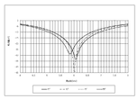
- FIG. 2 is a graph showing the relationship between the frequency of electromagnetic waves and the amount of absorption in the electromagnetic wave absorbing plate of Embodiment 1 of the present invention.
- the thing before vulcanization is made into the measurement object here from the problem of measurement efficiency.
- those skilled in the art will understand that the same electromagnetic wave absorption before and after vulcanization can be obtained by performing the necessary adjustment processing, so that the measurement data before vulcanization is not a problem. Let's go.
- the horizontal axis indicates the electromagnetic wave frequency [GHz]
- the vertical axis indicates the electromagnetic wave absorption [dB].
- the measurement results of the measurement results shown in FIG. 2 are the baking temperature of soybean hulls of about 900 [° C.], the content of burned soybean hulls with respect to the base material is about 200 [phr], the thickness of the electromagnetic wave absorbing plate (plate Thickness) is about 2.0 [mm].
- the electromagnetic wave absorbing plate of the present embodiment is about ⁇ 20 [dB]. dB] of electromagnetic wave absorption could be achieved.
- the electromagnetic wave absorbing plate of the present embodiment is characterized in that a desired amount of electromagnetic wave absorption can be realized when the incident angle is relatively small.
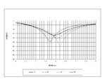
- FIG. 3 is a graph showing the relationship between the frequency of electromagnetic waves and the amount of absorption in the electromagnetic wave absorbing plate of Embodiment 2 of the present invention.
- the amount of electromagnetic wave absorbed [dB] when the content of the burned soybean hulls is increased by about 10%, that is, about 220 [phr], compared to that according to FIG. 2 is shown.
- 5.8 “GHz” band the only thing exceeding the standard required for the ETC system is when the incident angle is 55 °.
- changing the content of the burned plant according to the target frequency band is not the only parameter for determining the amount of electromagnetic wave absorption.
- the content of burned soybean hulls in the electromagnetic wave absorbing plate is one of the important parameters in determining the amount of electromagnetic wave absorption. It can also be seen that the thickness of the electromagnetic wave absorbing plate is one of the important parameters in determining the electromagnetic wave absorption amount. Therefore, the electromagnetic wave absorbing plate of the present embodiment is appropriately adjusted by adjusting the content of the burned soybean hulls under the condition that the thickness of the electromagnetic wave absorbing plate is about 2 mm, which can be said to be universal. Targeting electromagnetic waves in the "GHz" band.
- the reason why the thickness of the electromagnetic wave absorbing plate is usually about 2 mm is that when the plate thickness is relatively thin, the strength of the electromagnetic wave absorbing plate decreases, while the thickness of the electromagnetic wave absorbing plate is relatively This is because the thickness of the electromagnetic wave absorbing plate increases when it is thick. From this, it can be said that it is generally preferable to preferentially change the content of the burned plant.
- the electromagnetic wave absorbing plate of this embodiment can be suitably used in an ETC system or the like. Specifically, it can be attached to the ground, building ceiling, building wall, hallway, pillar, etc. near the ETC gate by pasting. Even at the time of enforcement, the electromagnetic wave absorbing plate of the present embodiment is relatively lightweight, so the burden on the installer is reduced.
- the electromagnetic wave absorbing plate of the present embodiment is also suitably used for the wall surface of an underground parking lot that controls the opening and closing of gates using 5.8 [GHz] radio waves as in the ETC system. be able to. Furthermore, it can be used suitably also for the wall surface of a tunnel for an inter-vehicle communication system countermeasure.
- FIG. 4 is a schematic partial manufacturing process diagram of the electromagnetic wave absorbing plate according to the third embodiment of the present invention.
- the manufacturing process of the burned soybean hull itself is the same as that described with reference to FIG.
- the carbonization baking temperature for producing the burned soybean hulls is about 900 ° C.
- the subsequent kneading process is performed in two stages, unlike the case described with reference to FIG. This is based on an empirical rule that the familiarity of naphthenic process oil and the like has been confirmed.
- a kneading process of the burned material of soybean hulls and ethylene / propylene diene rubber is performed.
- the kneader and the heating conditions are the same as those in the first embodiment, but the processing time can be slightly increased to 20 to 30 minutes.
- the content of burned soybean hulls with respect to ethylene / propylene diene rubber was about 200 [phr].
- the burned soybean hulls are contained in the ethylene / propylene diene rubber under the condition of about 1.4 kg / m 2 .
- these various conditions are examples, as in the description in the first embodiment.
- a second kneading step is performed.
- appropriate amounts of various additives such as naphthenic process oil are added to the kneaded product obtained by the first kneading step and kneaded.
- the kneading conditions may be a temperature of about 100 ° C., slightly lower than that in the first kneading step, and a treatment time of 20 to 30 minutes.
- the kneaded material obtained by performing the second kneading step is subjected to a rolling process.
- the rolling mill used in the present embodiment was also a mixing roll (15 inches wide) manufactured by Yanase Seisakusho. The rolling treatment is performed at room temperature, and the width between the surfaces of the rolls of the rolling mill can be about 1.8 mm to 2.2 mm.
- the width between the surfaces of the rolls of the rolling mill is mainly the content of the burned soybean hulls with respect to the base material such as ethylene / propylene diene rubber, various conditions in the first and second kneading steps, and the frequency used as the electromagnetic wave shielding target. It should be noted that it is determined based on the band and is not absolute.
- a vulcanization step is performed on the sheet-like electromagnetic wave absorbing plate material obtained by rolling (molding).
- the vulcanization treatment may be wet vulcanization or dry vulcanization. In this embodiment, a case where wet vulcanization is employed will be described.
- the vulcanization process is carried out using a steam pressure heating kiln, a high-temperature tank or the like.
- Steam pressure heating type kilns and the like are made of a material capable of performing steam heating, such as iron and aluminum.
- Vulcanization conditions may be determined according to the content of burned soybean hulls with respect to ethylene / propylene diene rubber. As an example, vulcanization conditions such as a treatment time of 30 minutes to 40 minutes at a temperature of about 140 ° C. to 150 ° C. under a steam pressure of 0.3 MPa to 0.4 MPa can be used.
- the above vulcanization conditions are examples when ethylene / propylene diene rubber is used as a base material. If the base material is changed to another, the vulcanization conditions are changed accordingly. It is.
- the electromagnetic wave absorbing plate After the vulcanization step, the electromagnetic wave absorbing plate has a thickness of about several millimeters made of fluorine, vinyl chloride or the like in the case of an outdoor usage environment, as described in the first embodiment.
- a sheet layer for preventing flooding may be formed.
- the electromagnetic wave absorbing plate of the present embodiment uses a burned soybean hull as its material, and it is known that the burned soybean hull has a porous structure. Therefore, when the electromagnetic wave absorbing plate material containing the burned material of soybean hulls is vulcanized, the air in the holes expands by heating during vulcanization, and the air appears as bubbles in the ethylene / propylene diene rubber, that is, It was found to foam. And it turned out that it is thought that this bubble contributes suitably, when converging the peak of the amount of absorption with respect to the incident angle of various electromagnetic waves so that it may mention later.
- FIG. 5 is a cross-sectional photograph of the electromagnetic wave absorbing plate obtained through the manufacturing process shown in FIG.
- FIG. 5A shows a cross-sectional photograph parallel to the surface direction of the electromagnetic wave absorbing plate
- FIG. 5B shows a cross-sectional photograph perpendicular to the surface direction of the electromagnetic wave absorbing plate.
- SEI images scanning secondary electron images
- JSM-5610 scanning analytical electron microscope
- FIG. 5A it can be seen that there are a plurality of substantially circular black regions having a size of about 200 ⁇ m in the cross section parallel to the surface direction of the electromagnetic wave absorbing plate of the present embodiment. These areas are voids. As a result of taking a cross-sectional photograph, there are many voids with an opening width of about 100 ⁇ m to 300 ⁇ m in the cross section parallel to the surface direction of the electromagnetic wave absorbing plate. Was about 200 ⁇ m.
- FIG. 5 (b) it can be seen that a plurality of substantially circular black regions having a size of about 400 ⁇ m are present in the cross section perpendicular to the surface direction of the electromagnetic wave absorbing plate of the present embodiment. These regions are also voids. As a result of taking a cross-sectional photograph, there were many voids with an opening width of about 200 ⁇ m to 500 ⁇ m in the cross section perpendicular to the surface direction of the electromagnetic wave absorbing plate. Was about 300 ⁇ m.
- the opening appearing in the vertical section is larger than the opening appearing in the section parallel to the surface direction of the electromagnetic wave absorbing plate. appear. Moreover, the presence of voids as shown in FIGS. 5A and 5B was also confirmed on the surface of the electromagnetic wave absorbing plate.
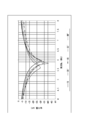
- FIG. 6 is a graph showing the relationship between the frequency of electromagnetic waves and the amount of absorption in the electromagnetic wave absorbing plate obtained through the manufacturing process shown in FIG. 4, and corresponds to FIG.
- the specific production conditions are as follows: the baking temperature of soybean hulls is about 900 [° C.], the content of burned soybean hulls with respect to the base material is about 200 [phr], the thickness of the electromagnetic wave absorbing plate before vulcanization (plate Thickness) is set to 2.08 [mm]. As a result, the finally produced electromagnetic wave absorbing plate has a thickness of about 2.6 mm to 2.7 mm through the vulcanization process.
- an electromagnetic wave incident at an angle of 15 ° with respect to an electromagnetic wave absorbing plate having a thickness of about 2.6 mm is calculated with respect to an electromagnetic wave absorbing plate having a thickness of about 2.69 mm, if calculated using the definition of Pythagoras. This is synonymous with perpendicular incidence.
- the thickness is about 3.00 mm at 30 °, about 3.68 mm at 45 °, about 4.53 mm at 55 °, and about 5.2 mm at 60 °. It is synonymous with perpendicularly incident on the electromagnetic wave absorbing plate.
- the peak of the electromagnetic wave absorption amount is easily converged to the target frequency band, so that the number of trial and error can be drastically reduced. This is considered because electromagnetic waves are effectively absorbed in the bubble portion in the electromagnetic wave absorbing plate.
- an electromagnetic wave absorbing plate is manufactured using a burned soybean hull is described as an example, but other plant burned products such as cottonseed meal, rapeseed meal, and cacao husk also have a porous structure. It is considered that the above-described effects can be obtained for the electromagnetic wave absorbing plate produced using these.
- FIG. 7 is a schematic manufacturing process diagram of the electromagnetic wave absorbing plate according to Embodiment 4 of the present invention. Only the vulcanization process is different from that shown in FIG. In the dry vulcanization process, a vulcanizer manufactured using a mold or a mold is used. This vulcanizer can be made of, for example, iron or copper. The lid part size of the vulcanizer can be set to 400 mm ⁇ 1200 mm ⁇ 15 mm, for example.
- the main body portion may be a size corresponding to the lid portion, and the edge portion may be secured, for example, about 50 mm from the end portion. What is necessary is just to determine the thickness of the hollow part located in the center of an edge part suitably according to the thickness of the electromagnetic wave absorption board to manufacture. This thickness can be set to, for example, about 2 mm to 3 mm. Of course, each of the above sizes is an example, and may be, for example, twice or more, or may be, for example, 1/2 or less.
- the thickness of the hollow portion needs to be equal to or greater than the width between the surfaces of the rolls of the rolling mill during the rolling process, that is, equal to or greater than the thickness of the sheet-like electromagnetic wave absorbing plate material obtained by the rolling process. If the two thicknesses are matched, the bubbles generated during vulcanization are removed by the main body portion and the lid portion of the vulcanizer and are removed to the outside through the gap. Even in such cases,
- the thickness of the electromagnetic wave absorbing plate material is secured about 0.5 mm from the thickness of the hollow portion, even if the thickness of the entire electromagnetic wave absorbing plate is increased by the expansion of bubbles, the upper limit of the thickness is defined by the lid portion. Is done. Thereby, an electromagnetic wave absorbing plate having no unevenness on the surface can be obtained. In this case, there is an advantage that it becomes easy to form a sheet layer for preventing water immersion thereafter.
- the hollow part cannot be made thinner than the electromagnetic wave absorbing plate material. This is because the electromagnetic wave absorbing plate material cannot be set in the hollow portion.
- FIG. 8 is a view showing a modification of the dry vulcanizing apparatus in the manufacturing process diagram shown in FIG.
- the vulcanizing apparatus shown in FIG. 8 is also referred to as a thermostatic bath, and performs a vulcanization process by electric power heating.
- the heating temperature can be set to 140 ° C. to 150 ° C.
- the vulcanization time can be set to 30 minutes to 40 minutes.
- this vulcanizing apparatus if it is used as it is, the surface smoothing as described with reference to FIG. 7 cannot be realized, but a space corresponding to the hollow portion shown in FIG. 7 is formed.
- the container was prepared, and the sheet-like electromagnetic wave absorbing plate material obtained by the rolling process was accommodated therein, and the entire container was put into the vulcanizing apparatus to perform the vulcanization process, which was described with reference to FIG. Such smoothing of the surface can be realized.
Landscapes
- Physics & Mathematics (AREA)
- Electromagnetism (AREA)
- Engineering & Computer Science (AREA)
- Microelectronics & Electronic Packaging (AREA)
- Shielding Devices Or Components To Electric Or Magnetic Fields (AREA)
Abstract
【課題】高度に電磁波を吸収し、かつ、比重が非常に軽量な電磁波吸収板を提供する。 【解決手段】エチレン・プロピレンジエンゴムなどの母材に、600[℃]から3000[℃]の範囲で焼成した大豆皮焼成物などの植物焼成物が含有されてなる電磁波吸収板であって、前記植物焼成物の含有率を150[phr]から250[phr]まで範囲とし、板厚を1.8[mm]から2.2[mm]までの範囲とし、選択的に、フッ素、塩化ビニルなどを素材とした、浸水防止用シート層を形成する。
Description
本発明は、植物焼成物及び電磁波遮蔽板に関し、特に、ETC(Electronic Toll Collection)システム、自動車間通信システムなどで用いられる5.8GHz帯の電磁波を吸収する植物焼成物及び電磁波吸収板に関する。
特許文献1には、植物炭及び金属酸化物誘電体を構成成分として含有する電磁波吸収体が開示されている。特許文献1によれば、植物炭と共に、高周波電磁波吸収能を有する金属酸化物誘電体を含有させたものは、その相乗効果により、GHz帯の電磁波を効率的に吸収することができ、この電磁波吸収体は、建物の天井、壁、床の下地ボードとして十分な強度を有すると記載されている。
しかし、特許文献1に開示されている電磁波吸収体は、以下の点で問題がある。すなわち、第1に、特許文献1に開示されている電磁波吸収体は、GHz帯の電磁波を効率的に吸収することができるとされているものの、GHz帯の電磁波の吸収レベルも限定的である。
第2に、特許文献1に開示されている電磁波吸収体は、植物炭を含有させているため、比重が軽くなった旨が発明の効果であるとして明記されている。しかし、この電磁波吸収体は、金属酸化物誘電体が少なくとも重量比で全体の20%以上、最も好ましい場合で50%以上含まれているので、たとえ、植物炭が含有されていたとしても、電磁波吸収体の比重は、相対的に、軽いものであると評価することはできず、その自重から建物の天井、壁の下地ボードには使用しにくいという問題がある。
そこで、本発明は、高度に電磁波を吸収し、かつ、比重が非常に軽量な電磁波吸収板を提供することを課題とする。
また、本発明は、上記電磁波吸収板に用いられる植物焼成物を提供することを課題とする。
上記課題を解決するために、本発明は、母材に植物焼成物が含有されてなる電磁波吸収板であって、
前記植物焼成物の含有率を150[phr]から250[phr]までの範囲で選択し、
板厚を1.8[mm]から2.2[mm]までの範囲で選択することによって、
電磁波吸収板に対して電磁波の入射角が55°の場合に-15[dB]以上の吸収量となる電磁波吸収板である。
前記植物焼成物の含有率を150[phr]から250[phr]までの範囲で選択し、
板厚を1.8[mm]から2.2[mm]までの範囲で選択することによって、
電磁波吸収板に対して電磁波の入射角が55°の場合に-15[dB]以上の吸収量となる電磁波吸収板である。
さらに、この電磁波吸収板の表面には、フッ素、塩化ビニルなどを素材とした、浸水防止用シート層を形成するとよい。
また、本発明は、上記電磁波吸収板に用いられる植物焼成物であって、炭化に必要な条件(概ね、600[℃]以上)で焼成している。
以下、本発明の実施形態について図面を参照して説明する。
(実施形態1)
まず、本実施形態の電磁波吸収板の概要について説明する。本実施形態では、大豆皮を炭化焼成することによって、植物焼成物であるところの大豆皮焼成物を製造する。ここで、大豆を原材料として食用油等を製造することによって、大量の大豆皮が発生している。これらの大半は牧畜用の飼料や農業用の肥料に再利用されているが、更なる用途も模索されている。エコロジーの観点から日夜研究した結果、大豆皮の更なる再利用として、大豆皮焼成物が、電磁波吸収板に有益に用いられることを見出した。
まず、本実施形態の電磁波吸収板の概要について説明する。本実施形態では、大豆皮を炭化焼成することによって、植物焼成物であるところの大豆皮焼成物を製造する。ここで、大豆を原材料として食用油等を製造することによって、大量の大豆皮が発生している。これらの大半は牧畜用の飼料や農業用の肥料に再利用されているが、更なる用途も模索されている。エコロジーの観点から日夜研究した結果、大豆皮の更なる再利用として、大豆皮焼成物が、電磁波吸収板に有益に用いられることを見出した。
大豆皮焼成物は、例えば約600[℃]~3000[℃]の温度で、静置炉、ロータリーキルンなどの炭化装置を用いて、選択的に、窒素ガス等の不活性ガス雰囲気下或いは真空中で大豆皮等を到達温度で約3時間程度焼成することによって得る。ここで、この焼成温度、焼成時間は、大豆皮焼成物に対して焙煎を超えて炭化するために必要な条件とすればよい。したがって、炭化装置の種別、炭化処理時の大豆皮の処理量などによって多少相違する点に留意されたい。
また、研究・実験を重ねた結果、大豆皮焼成物は、粉砕しないで用いると良いことが分かった。ここでいう、「粉砕しないで用いる」とは、大豆皮焼成物に対して粉砕処理を施していないことのみならず、大豆を原材料として食用油等を製造する際に発生する大豆皮自体に対しても粉砕処理を施していないし、つまり、いわゆる素焼きの状態のものを用いるという意味である。
すなわち、粉砕しない大豆皮焼成物を、後述する条件で母材に配合することによって製造した電磁波吸収板は、粉砕した大豆皮焼成物を用いて製造した場合に比して、少なくとも5.8[GHz]帯の電磁波では、その吸収効率が良いことがわかった。
粉砕しない大豆皮焼成物について、嵩密度及び充填密度を計測してみた。嵩密度及び充填密度の経時変化の有無も調査すべく、2008年10月に製造した大豆皮焼成物、2009年3月に製造した大豆皮焼成物、2010年9月に製造した大豆皮焼成物の各々の乾燥品を計測対象とした。なお、いずれの大豆皮焼成物も、焼成温度は約900℃とした。また、嵩密度及び充填密度の計測手法は、JIS K 1474規格に基づく。
2008年10月に製造した大豆皮焼成物の場合、嵩密度は0.092[g/ml]で、充填密度は0.203[g/ml]であった。
2009年3月に製造した大豆皮焼成物の場合、嵩密度は0.0895[g/ml]で、充填密度は0.1828[g/ml]であった。
2010年9月に製造した大豆皮焼成物の場合、嵩密度は0.088[g/ml]で、充填密度は0.187[g/ml]であった。
以上の計測結果から、嵩密度及び充填密度の経時変化はないといえる。また、嵩密度は、概ね0.08[g/ml]~0.1[g/ml]の範囲内と考えられ、充填密度は、概ね0.18[g/ml]~0.25[g/ml]の範囲内であると考えられる。
本実施形態では、この大豆皮焼成物を、母材であるところのエチレン・プロピレンジエンゴム、シリコンゴム、低密度ポリエチレン、イソプレン、ウレタン、ガラスウール、ポリ塩化ビニル樹脂などに対して配合する。母材は、耐熱性、成形性に優れたものが好ましい。なお、以下、特に断りがない限り、母材としては、エチレン・プロピレンジエンゴムを用いた例について説明する。
つぎに、大豆皮焼成物を、エチレン・プロピレンジエンゴムに対して、例えば約150[phr]~約250[phr](per hundred resin(rubber))の量で配合する。その後、当該ゴムを加硫及び成形すれば、最終製品である電磁波吸収板が得られる。
図1は、本発明の実施形態1の電磁波吸収板の模式的な製造工程図である。まず、食用油等の製造時に発生する生大豆皮を、選択的に、レゾール型フェノール樹脂等のフェノール樹脂を含有させてから炭化装置にセットして、窒素ガス雰囲気下で1分当たり約2[℃]ずつ温度を上昇させ、600[℃]~1500[℃](たとえば900[℃])といった所定の温度まで到達させる。
レゾール型フェノール樹脂等を混合すると、大豆皮焼成物の強度、炭素量の向上を図ることができる。もっとも、当該混合自体は、本実施形態の電磁波吸収板の製造上、必ずしも必要ではない点に留意されたい。
それから、到達温度で3時間程度、炭化焼成処理を施す。なお、既述のように、粉砕しない大豆皮焼成物を用いて電磁波吸収板を製造した方が好ましいことから、電磁波吸収のためには、大豆皮焼成物の径や形状にばらつきがあった方が良いといえる。このため、一般的には、炭化焼成温度は、600[℃]程度の、相対的に低温である方が好ましいともいえる。
つぎに、大豆皮焼成物とエチレン・プロピレンジエンゴムとを、ナフテン系プロセスオイル、芳香族系プロセスオイル、パラフィン系プロセスオイルなどの各種添加剤とともに、混練機にセットして混練処理する。
本実施形態では、混練機として、株式会社モリヤマ製の加圧型ニーダー(DS20-40)を用いた。そして、約110℃の温度下で、混練処理時間は約20分とした。もっとも、加温条件、処理時間は一例であり、これらに限定されるものではなく、加温条件は、例えば90℃~120℃、処理時間は、例えば5分~25分程度の範囲でよい。
それから、混練物の十分な冷却時間を経てから、圧延処理を施す。本実施形態では、圧延機として、柳瀬製作所製のミキシングロール(15インチ幅)を用いた。圧延処理は、常温下で行った。もっとも、これらの圧延条件は一例であり、限定的ではなく、10インチ幅~20インチ幅程度の範囲での処理としてもよいし、多少の加温等した環境下での処理としてもよい。
その後、所要の加硫処理を行うと、電磁波吸収板の製造が完了する。この電磁波吸収板は、屋外などの使用環境の場合には、フッ素、塩化ビニルなどを素材とした、数mm程度の厚さの浸水防止用シート層を形成するとよい。
本実施形態における電磁波吸収板の製造工程では、大豆皮焼成物が粉砕されにくいので、大豆皮焼成物の径を相対的に大きな状態で、かつ、ランダムな形状が維持されるようため、効果的な電磁波吸収を実現できる。
図2は、本発明の実施形態1の電磁波吸収板における電磁波の周波数とその吸収量との関係を示すグラフである。なお、ここでは、計測効率の問題から、加硫前のものを測定対象としている。もっとも、当業者であれば、所要の調整処理を施せば、加硫前後で同様の電磁波吸収量が得られるので、加硫前の計測データであることは問題とならないことは理解されるであろう。
図2の横軸は電磁波の周波数[GHz]を示し、縦軸は電磁波の吸収量[dB]を示している。また、図2に示す測定結果の測定対象は、大豆皮の焼成温度を約900[℃]、母材に対する大豆皮焼成物の含有率を約200[phr]、電磁波吸収板の厚さ(板厚)を約2.0[mm]としている。
なお、この計測は、2010年11月13日に防衛大学校電波暗室にて、自由空間法により行った。ここでは、電磁波吸収板に対して、15°,30°,45°,55°の角度で電磁波を入射させた場合の電磁波吸収量を計測した。
図2に示すように、いわゆる5.8[GHz]帯では、
電磁波の入射角が15°の場合には約-28[dB]、
電磁波の入射角が30°の場合には約-21[dB]、
電磁波の入射角が45°の場合には約-20[dB]、
電磁波の入射角が55°の場合には約-20[dB]、
となった。
電磁波の入射角が15°の場合には約-28[dB]、
電磁波の入射角が30°の場合には約-21[dB]、
電磁波の入射角が45°の場合には約-20[dB]、
電磁波の入射角が55°の場合には約-20[dB]、
となった。
ここで、ETCシステムでは、5.8[GHz]帯の電磁波の場合には、概ね
入射角が15°の場合には-25[dB]以上、
入射角が30°の場合には-20[dB]以上、
入射角が45°の場合には-20[dB]以上、
入射角が55°の場合には-15[dB]以上、
の吸収量が要求されている。
入射角が15°の場合には-25[dB]以上、
入射角が30°の場合には-20[dB]以上、
入射角が45°の場合には-20[dB]以上、
入射角が55°の場合には-15[dB]以上、
の吸収量が要求されている。
特に、入射角が55°という斜入射に対して、-15[dB]以上の吸収量を実現することは一般的には困難であるが、本実施形態の電磁波吸収板は、約-20[dB]の電磁波吸収量を達成することができた。換言すると、本実施形態の電磁波吸収板は、入射角が相対的に小さな場合に、所望の電磁波吸収量を実現できる点が特徴である。
(実施形態2)
図3は、本発明の実施形態2の電磁波吸収板における電磁波の周波数とその吸収量との関係を示すグラフである。ここでは、図2に係るものに比して、大豆皮焼成物の含有率を約10%増加、すなわち約220[phr]に変更した場合の電磁波の吸収量[dB]を示している。係る場合には、いわゆる5.8「GHz」帯では、ETCシステムで要求される基準を超えるものは、入射角が55°の場合のみである。
図3は、本発明の実施形態2の電磁波吸収板における電磁波の周波数とその吸収量との関係を示すグラフである。ここでは、図2に係るものに比して、大豆皮焼成物の含有率を約10%増加、すなわち約220[phr]に変更した場合の電磁波の吸収量[dB]を示している。係る場合には、いわゆる5.8「GHz」帯では、ETCシステムで要求される基準を超えるものは、入射角が55°の場合のみである。
もっとも、技術的に見れば、ターゲットとする周波数帯域に応じて、植物焼成物の含有率を変化させることが、電磁波吸収量を決定する上での唯一のパラメータではない。例えば、電磁波吸収板の板厚を変更することでも、ターゲットとなる周波数帯域を変更することは可能である。電磁波吸収板の誘電率が変わるためである。したがって、大豆皮焼成物の含有率を約10%増加させた場合であっても、電磁波吸収板の板厚を適宜変更すれば、図2に示した場合と同様に、所望の電磁波吸収量を達成することができる。
以上を纏めると、電磁波吸収板における大豆皮焼成物の含有率が、電磁波吸収量を決定する上で、重要なパラメータの一つであることが分かる。また、電磁波吸収板の板厚も電磁波吸収量を決定する上で、重要なパラメータの一つであることが分かる。そこで、本実施形態の電磁波吸収板は、電磁波吸収板の板厚として汎用的ともいえる2mm程度の板厚という条件下で、大豆皮焼成物の含有率を適宜調整することにより、5.8「GHz」帯の電磁波をターゲットとしている。
ただし、電磁波吸収板の板厚が、通常、2mm程度とされている理由は、当該板厚が相対的に薄い場合には電磁波吸収板の強度が低下する一方で、当該板厚が相対的に厚い場合には電磁波吸収板の重量が増加するためである。このことから、一般的には、植物焼成物の含有率を優先的に変化させることが好ましいといえる。
本実施形態の電磁波吸収板は、ETCシステム等で好適に用いることができる。具体的には、ETCゲート付近の地面・建物天井・建物壁面・廊下・柱などに、貼付による施工で取り付けることができる。この施行時にも、本実施形態の電磁波吸収板は、相対的に軽量であるため、施工者の負担軽減になる。
また、本実施形態の電磁波吸収板は、ETCシステムの他にも、ETCシステムと同様に5.8[GHz]の電波を用いてゲートの開閉を制御する地下駐車場の壁面にも好適に用いることができる。さらに、自動車間通信システム対策用としてトンネルの壁面にも好適に用いることができる。
(実施形態3)
図4は、本発明の実施形態3の電磁波吸収板の模式的な一部の製造工程図である。まず、大豆皮焼成物自体の製造工程は、図1を用いて説明した場合と同様である。本実施形態では、大豆皮焼成物を製造するための炭化焼成温度は約900℃としている。その後の混練処理は、図1を用いて説明した場合と異なり、2段階に分けて実施している。これは、こうしたところ、ナフテン系プロセスオイル等のなじみやすさを確認できたという経験則に基づくものである。
図4は、本発明の実施形態3の電磁波吸収板の模式的な一部の製造工程図である。まず、大豆皮焼成物自体の製造工程は、図1を用いて説明した場合と同様である。本実施形態では、大豆皮焼成物を製造するための炭化焼成温度は約900℃としている。その後の混練処理は、図1を用いて説明した場合と異なり、2段階に分けて実施している。これは、こうしたところ、ナフテン系プロセスオイル等のなじみやすさを確認できたという経験則に基づくものである。
第1の混練工程では、大豆皮焼成物とエチレン・プロピレンジエンゴムとの混練処理を行う。ここでは、混練機及び加温条件は、実施形態1と同じとしたが、処理時間は20分~30分と多少増加させることもできる。また、エチレン・プロピレンジエンゴムに対する大豆皮焼成物の含有率は、約200[phr]とした。換言すると、エチレン・プロピレンジエンゴムに対して大豆皮焼成物を、約1.4kg/m2となる条件で含有させている。のもっとも、実施形態1での説明と同様に、これらの各種条件は一例である点に留意されたい。
つぎに、第2の混練工程を実施する。本工程では、第1の混練工程の実施によって得られた混練物に対して、実施形態1の場合と同様に、ナフテン系プロセスオイル等の各種添加剤を適量添加して混練処理する。混練条件は、第1の混練工程の場合よりも若干低温の約100℃の温度とし、20分~30分の処理時間とすることができる。
それから、実施形態1と同様に、第2の混練工程の実施によって得られた混練物に対して圧延処理を施す。本実施形態で用いる圧延機も、柳瀬製作所製のミキシングロール(15インチ幅)とした。圧延処理は常温下で行い、圧延機のロールの表面間幅は、1.8mm~2.2mm程度とすることができる。
圧延機のロールの表面間幅は、主として、エチレン・プロピレンジエンゴム等の母材に対する大豆皮焼成物の含有率、第1及び第2の混練工程における各種条件と、電磁波の遮蔽ターゲットとする周波数帯とに基づいて決定されるものであり、絶対的なものではない点に留意されたい。
つぎに、圧延処理(成形処理)によって得られたシート状の電磁波吸収板材料に対して加硫工程を実施する。加硫処理は、湿式加硫としてもよいし、乾式加硫としてもよい。本実施形態では、湿式加硫を採用した場合について説明する。
加硫工程は、蒸気圧加熱型窯、高温槽などを用いて実施する。蒸気圧加熱型窯等は、鉄、アルミニウムなどの蒸気加熱を行うことができる材料によって製造されている。加硫条件は、エチレン・プロピレンジエンゴムに対する大豆皮焼成物の含有率に応じて決定すればよ。一例としては、0.3MPa~0.4MPaの蒸気加圧下で、約140℃~150℃の温度で、30分~40分の処理時間といった加硫条件とすることができる。
もっというと、上記の加硫条件は、母材としてエチレン・プロピレンジエンゴムを用いた場合の例示であり、母材が他のものに変更されれば、それに応じて、加硫条件も変更されるのである。
加硫工程後には、この電磁波吸収板には、実施形態1での説明と同様に、屋外などの使用環境の場合には、フッ素、塩化ビニルなどを素材とした、数mm程度の厚さの浸水防止用シート層を形成するとよい。
ここで、本実施形態の電磁波吸収板では、その材料として、大豆皮焼成物を用いており、大豆皮焼成物は、ポーラス構造であることが知られている。したがって、大豆皮焼成物を含む電磁波吸収板材料を加硫すると、加硫時の加熱によって孔内の空気が膨張し、その空気が、エチレン・プロピレンジエンゴム内に気泡となって現れる、すなわち、発泡することがわかった。そして、この気泡は、後述するように、様々な電磁波の入射角に対する吸収量のピークを収束させる際に好適に寄与すると考えられることが分かった。
図5は、図4に示す製造工程を経て得られた電磁波吸収板の断面写真である。図5(a)には電磁波吸収板の面方向に平行な断面写真を示し、図5(b)には電磁波吸収板の面方向に垂直な断面写真を示している。いずれも、日本電子株式会社製の走査型分析電子顕微鏡(JSM-5610)を用いて撮像した走査二次電子像(SEI画像)であり、それぞれ、35倍の倍率で撮影したものである。
図5(a)に示すように、本実施形態の電磁波吸収板の面方向に平行な断面には、約200μmほどの大きさの略円形の黒色の領域が複数存在していることが分かる。これらの領域は空隙である。断面写真の撮影時で確認できたものとしては、電磁波吸収板の面方向に平行な断面には、約100μm~300μmほどの開口幅の空隙が多数存在しており、平均的な空隙の開口幅は約200μmほどであった。
図5(b)に示すように、本実施形態の電磁波吸収板の面方向に垂直な断面には、約400μmほどの大きさの略円形の黒色の領域が複数存在していることが分かる。これらの領域も空隙である。断面写真の撮影時で確認できたものとしては、電磁波吸収板の面方向に垂直な断面には、約200μm~500μmほどの開口幅の空隙が多数存在しており、平均的な空隙の開口幅は約300μmほどであった。
図5(a)及び図5(b)に示す断面写真によれば、電磁波吸収板の面方向に平行な断面に現れる空隙よりも、垂直な断面に現れる空隙の方が、その開口部が大きく見える。また、電磁波吸収板の表面にも、図5(a)及び図5(b)に示すような空隙の存在が確認できた。
図6は、図4に示す製造工程を経て得られた電磁波吸収板における電磁波の周波数とその吸収量との関係を示すグラフであり、図2に対応するものである。具板的な製造条件としては、大豆皮の焼成温度を約900[℃]、母材に対する大豆皮焼成物の含有率を約200[phr]、加硫前の電磁波吸収板の厚さ(板厚)を2.08[mm]としている。この結果として、最終的に製造される電磁波吸収板は、加硫工程を経ることによって、約2.6mm~2.7mmの厚さとなった。
図6に示すグラフによれば、図2との対比により明らかなように、略同一の結果、すなわち、略同一の電磁波吸収量が実現できていることが分かる。加えて、この効果以外にも、本実施形態では、ターゲットとする周波数帯域を5.8GHzに対して、各電磁波入射角のピークを収束させられていることが分かる。本実施形態の電磁波吸収板の製造条件を、実施形態1のものと略同一としていることから、当該ピークの収束は、加硫工程において発生する気泡によって得られる効果であるといえよう。
なお、約2.6mmの厚さの電磁波吸収板に対して15°の角度で入射する電磁波は、ピタゴラスの定義を用いて算出すれば、約2.69mmの厚さの電磁波吸収板に対して垂直に入射することと同義である。同様に、それぞれ、30°の場合には約3.00mm、45°の場合には約3.68mm、55°の場合には約4.53mm、60°の場合には約5.2mmといった厚さの電磁波吸収板に対して垂直に入射することと同義である。
ここで、当業者であれば、吸収ピークに着眼した場合に、電磁波吸収板の厚さが異なることで、ターゲットとなる周波数帯がずれることが常識的であると考えるはずである。とすれば、上記のように、電磁波吸収板の厚さが電磁波の入射角に換算して最大で2倍程度も異なるにも拘わらず、ターゲットとなる周波数帯に電磁波吸収量のピークを収束させられる点は、当業者にとってみても、本実施形態の電磁波吸収板の効果として注目に値するといえる。
なぜなら、通常、電磁波吸収技術分野の当業者であれば、所望の周波数帯において所望の電磁波吸収量を実現できるように、種々のパラメータをトライアンドエラーによって選択して電磁波吸収板を製造している。つまり、例えば、5.8[GHz]という周波数帯において、様々な入射角の電磁波を効果的に吸収できるようにするためには、エチレン・プロピレンジエンゴムに対する大豆皮焼成物の含有率を変更したり、混練条件、圧延処理、加硫条件を変更したりしながら電磁波吸収板を製造するといった労力を要する。
これに対して、本実施形態の電磁波吸収板の場合には、ターゲットとなる周波数帯に電磁波吸収量のピークを収束させやすくなることから、トライアンドエラーの回数を激減させることができる。これは、電磁波吸収板内の気泡部分において、電磁波が効果的に吸収されるためと考えられる。
以上、本実施形態では、大豆皮焼成物を用いて電磁波吸収板を製造する場合を例に説明したが、綿実粕、菜種粕、カカオハスクといった他の植物焼成物も、ポーラス構造であることから、これらを用いて製造する電磁波吸収板についても、上記のような効果が得られると考えられる。
(実施形態4)
図7は、本発明の実施形態4の電磁波吸収板の模式的な製造工程図である。図4に示したものとは、加硫工程が異なるだけである。乾式加硫工程では、金型又は鋳型によって製造した加硫装置を用いる。この加硫装置は、例えば、鉄製、銅製などとすることができる。加硫装置の蓋部サイズは、例えば、400mm×1200mm×15mmとすることができる。
図7は、本発明の実施形態4の電磁波吸収板の模式的な製造工程図である。図4に示したものとは、加硫工程が異なるだけである。乾式加硫工程では、金型又は鋳型によって製造した加硫装置を用いる。この加硫装置は、例えば、鉄製、銅製などとすることができる。加硫装置の蓋部サイズは、例えば、400mm×1200mm×15mmとすることができる。
本体部は、蓋部に対応するサイズとすればよく、縁部分は端部から例えば50mm程度確保すればよい。縁部分の中央に位置する中空部分は、製造したい電磁波吸収板の厚さに応じて、その厚さを適宜決定すればよい。この厚さとしては、例えば、2mm~3mm程度とすることができる。もちろん、上記各サイズは、一例であり、例えば2倍以上の大きさのものとしてもよいし、例えば1/2以下の大きさのものとしてもよい。
ただし、中空部分の厚さは、圧延処理の際における圧延機のロールの表面間幅以上、すなわち、圧延処理によって得られたシート状の電磁波吸収板材料の厚さ以上とする必要がある。仮に、両厚さを一致させると、加硫の際に発生する気泡は、加硫装置の本体部と蓋部とによって行き場をなくし、それらの隙間を通じて外部に脱せられることになる。係る場合であっても、
一方、中空部分の厚さより電磁波吸収板材料の厚さを0.5mm程度確保しておけば、気泡の膨張によって電磁波吸収板全体の厚みが増していっても、その厚み上限が蓋部によって規定される。これにより、表面に凹凸差のない電磁波吸収板を得ることができる。こうすると、その後に、浸水防止用シート層の形成が容易になるなどの利点がある。
反対に、中空部分は、電磁波吸収板材料よりも薄くすることはできない。中空部分内に、電磁波吸収板材料をセットすることができないためである。
図8は、図7に示す製造工程図における乾式の加硫装置の変形例を示す図である。図8に示す加硫装置は、恒温槽とも称され、電力加熱によって加硫工程を実施するものである。本実施形態の電磁波吸収板を製造するためには、加熱温度を140℃~150℃とし、加硫時間を30分~40分とすることができる。
この加硫装置の場合には、このままの使用をするのであれば、図7を用いて説明したような表面の平滑化を実現できないが、図7に示した中空部分に相当する空間を形成する容器を用意し、そこに圧延処理によって得られたシート状の電磁波吸収板材料を収容した状態で、容器ごと加硫装置に投入して加硫処理を行うことで、図7を用いて説明したような表面の平滑化を実現することができる。
Claims (4)
- 母材に植物焼成物が含有されてなる電磁波吸収板であって、
前記植物焼成物の含有率を150[phr]から250[phr]までの範囲で選択し、
板厚を1.8[mm]から2.2[mm]までの範囲で選択することによって、
電磁波吸収板に対して電磁波の入射角が55°の場合に-15[dB]以上の吸収量となる電磁波吸収板。 - さらに、表面に浸水防止用シート層が形成されている、請求項1記載の電磁波吸収板。
- 前記植物焼成物の孔内の気体が発泡する条件で加硫されている、請求項1記載の電磁波吸収板。
- 請求項1記載の電磁波吸収板に用いられる植物焼成物であって、炭化に必要な条件で焼成している植物焼成物。
Priority Applications (1)
| Application Number | Priority Date | Filing Date | Title |
|---|---|---|---|
| JP2011553993A JPWO2012086719A1 (ja) | 2010-12-22 | 2011-12-21 | 植物焼成物及び電磁波吸収板 |
Applications Claiming Priority (4)
| Application Number | Priority Date | Filing Date | Title |
|---|---|---|---|
| JP2010-286444 | 2010-12-22 | ||
| JP2010286444 | 2010-12-22 | ||
| JP2011100494 | 2011-04-28 | ||
| JP2011-100494 | 2011-04-28 |
Publications (1)
| Publication Number | Publication Date |
|---|---|
| WO2012086719A1 true WO2012086719A1 (ja) | 2012-06-28 |
Family
ID=46313987
Family Applications (1)
| Application Number | Title | Priority Date | Filing Date |
|---|---|---|---|
| PCT/JP2011/079713 Ceased WO2012086719A1 (ja) | 2010-12-22 | 2011-12-21 | 植物焼成物及び電磁波吸収板 |
Country Status (2)
| Country | Link |
|---|---|
| JP (1) | JPWO2012086719A1 (ja) |
| WO (1) | WO2012086719A1 (ja) |
Citations (8)
| Publication number | Priority date | Publication date | Assignee | Title |
|---|---|---|---|---|
| JPS59152696A (ja) * | 1983-02-19 | 1984-08-31 | アイン・エンジニアリング株式会社 | 電磁シ−ルド複合材の成形方法 |
| JP2001311105A (ja) * | 2000-05-01 | 2001-11-09 | Takenaka Komuten Co Ltd | 電磁波吸収特性を有する粒状材料と、電磁波吸収材料及びこれらの製造方法 |
| JP2002141691A (ja) * | 2000-11-01 | 2002-05-17 | Kaneha:Kk | 電波吸収体 |
| JP2005317825A (ja) * | 2004-04-30 | 2005-11-10 | Denki Kagaku Kogyo Kk | 電磁波吸収体 |
| JP2008130749A (ja) * | 2006-11-20 | 2008-06-05 | Konoshima Chemical Co Ltd | 不燃性電波吸収板 |
| JP2008282862A (ja) * | 2007-05-08 | 2008-11-20 | Kokoku Intech Co Ltd | 電波吸収体用組成物、電波吸収体及び電波吸収体の製造方法 |
| JP2009152374A (ja) * | 2007-12-20 | 2009-07-09 | Kaneha:Kk | 電波吸収体 |
| WO2010035829A1 (ja) * | 2008-09-29 | 2010-04-01 | 日清オイリオグループ株式会社 | 植物焼成物及び電磁波遮蔽体 |
-
2011
- 2011-12-21 WO PCT/JP2011/079713 patent/WO2012086719A1/ja not_active Ceased
- 2011-12-21 JP JP2011553993A patent/JPWO2012086719A1/ja not_active Revoked
Patent Citations (8)
| Publication number | Priority date | Publication date | Assignee | Title |
|---|---|---|---|---|
| JPS59152696A (ja) * | 1983-02-19 | 1984-08-31 | アイン・エンジニアリング株式会社 | 電磁シ−ルド複合材の成形方法 |
| JP2001311105A (ja) * | 2000-05-01 | 2001-11-09 | Takenaka Komuten Co Ltd | 電磁波吸収特性を有する粒状材料と、電磁波吸収材料及びこれらの製造方法 |
| JP2002141691A (ja) * | 2000-11-01 | 2002-05-17 | Kaneha:Kk | 電波吸収体 |
| JP2005317825A (ja) * | 2004-04-30 | 2005-11-10 | Denki Kagaku Kogyo Kk | 電磁波吸収体 |
| JP2008130749A (ja) * | 2006-11-20 | 2008-06-05 | Konoshima Chemical Co Ltd | 不燃性電波吸収板 |
| JP2008282862A (ja) * | 2007-05-08 | 2008-11-20 | Kokoku Intech Co Ltd | 電波吸収体用組成物、電波吸収体及び電波吸収体の製造方法 |
| JP2009152374A (ja) * | 2007-12-20 | 2009-07-09 | Kaneha:Kk | 電波吸収体 |
| WO2010035829A1 (ja) * | 2008-09-29 | 2010-04-01 | 日清オイリオグループ株式会社 | 植物焼成物及び電磁波遮蔽体 |
Also Published As
| Publication number | Publication date |
|---|---|
| JPWO2012086719A1 (ja) | 2014-06-05 |
Similar Documents
| Publication | Publication Date | Title |
|---|---|---|
| ES2719281T3 (es) | Procedimiento de preparación de placa de aislamiento térmico de cerámica de peso ligero de cocción rápida de baja temperatura | |
| CN110835240B (zh) | 一种粉煤灰陶粒及其制备方法 | |
| CN103342578A (zh) | 利用铁尾矿制备的多孔保温装饰材料及其制备方法 | |
| JP2017507110A5 (ja) | ||
| CN105948712A (zh) | 一种利用电解锰渣制备的陶瓷及其制备方法 | |
| KR101758634B1 (ko) | 폐유리를 이용한 다공성 세라믹 단열 내외장재의 조성물 및 제조방법 | |
| CN107032742A (zh) | 膨胀珍珠岩保温板的制备方法 | |
| CN105602078A (zh) | 一种膨胀型阻燃eva泡沫复合材料及其制备方法和应用 | |
| WO2012086719A1 (ja) | 植物焼成物及び電磁波吸収板 | |
| KR101438661B1 (ko) | 발포유리 제조용 성형체, 이의 제조 방법 및 이를 이용한 발포유리의 제조 방법 | |
| CN100369842C (zh) | 一种泡沫玻璃的制备方法 | |
| CN104445934A (zh) | 一种耐高温的尖劈形吸波材料及其制备方法 | |
| WO1996000800A1 (en) | Sintered steel manufacturing process | |
| KR100916534B1 (ko) | 폐고무발포체를 이용한 고무발포체 및 그 제조방법 | |
| KR102021758B1 (ko) | 고주파 흡수 및 방열 특성을 갖는 복합 시트, 그 제조 방법, 및 그 원료 | |
| CN120647348A (zh) | 一种多层板结构复合高温吸波陶瓷的制备方法 | |
| CN115394946B (zh) | 大规格方石墨电极的制备方法 | |
| JP4991096B2 (ja) | MgO蒸着材 | |
| KR20170014794A (ko) | 무기물질 분말을 이용한 진공캡슐 및 그 제조방법 | |
| CN115746459A (zh) | 一种高介电聚丙烯微发泡材料及其超临界流体模压发泡制备方法 | |
| CN109706295B (zh) | 一种片状Fe基合金粉体的新型退火工艺 | |
| KR20220111040A (ko) | 펄라이트 단열재 제조장치 및 방법 | |
| KR20170047699A (ko) | 왕겨를 접착. 성형한 판넬. | |
| KR101516404B1 (ko) | 자동차의 공조장치용 에어 덕트의 제조방법 | |
| CN109824935B (zh) | 一种聚苯乙烯泡沫保温板生产工艺 |
Legal Events
| Date | Code | Title | Description |
|---|---|---|---|
| WWE | Wipo information: entry into national phase |
Ref document number: 2011553993 Country of ref document: JP |
|
| 121 | Ep: the epo has been informed by wipo that ep was designated in this application |
Ref document number: 11851884 Country of ref document: EP Kind code of ref document: A1 |
|
| NENP | Non-entry into the national phase |
Ref country code: DE |
|
| 122 | Ep: pct application non-entry in european phase |
Ref document number: 11851884 Country of ref document: EP Kind code of ref document: A1 |