WO2012086530A1 - アンテナ装置、アンテナモジュールおよび携帯端末 - Google Patents
アンテナ装置、アンテナモジュールおよび携帯端末 Download PDFInfo
- Publication number
- WO2012086530A1 WO2012086530A1 PCT/JP2011/079136 JP2011079136W WO2012086530A1 WO 2012086530 A1 WO2012086530 A1 WO 2012086530A1 JP 2011079136 W JP2011079136 W JP 2011079136W WO 2012086530 A1 WO2012086530 A1 WO 2012086530A1
- Authority
- WO
- WIPO (PCT)
- Prior art keywords
- power supply
- point
- switch
- antenna
- antenna device
- Prior art date
- Legal status (The legal status is an assumption and is not a legal conclusion. Google has not performed a legal analysis and makes no representation as to the accuracy of the status listed.)
- Ceased
Links
Images







Classifications
-
- H—ELECTRICITY
- H01—ELECTRIC ELEMENTS
- H01Q—ANTENNAS, i.e. RADIO AERIALS
- H01Q9/00—Electrically-short antennas having dimensions not more than twice the operating wavelength and consisting of conductive active radiating elements
- H01Q9/04—Resonant antennas
- H01Q9/0407—Substantially flat resonant element parallel to ground plane, e.g. patch antenna
- H01Q9/045—Substantially flat resonant element parallel to ground plane, e.g. patch antenna with particular feeding means
-
- H—ELECTRICITY
- H01—ELECTRIC ELEMENTS
- H01Q—ANTENNAS, i.e. RADIO AERIALS
- H01Q1/00—Details of, or arrangements associated with, antennas
- H01Q1/12—Supports; Mounting means
- H01Q1/22—Supports; Mounting means by structural association with other equipment or articles
- H01Q1/24—Supports; Mounting means by structural association with other equipment or articles with receiving set
- H01Q1/241—Supports; Mounting means by structural association with other equipment or articles with receiving set used in mobile communications, e.g. GSM
- H01Q1/242—Supports; Mounting means by structural association with other equipment or articles with receiving set used in mobile communications, e.g. GSM specially adapted for hand-held use
- H01Q1/243—Supports; Mounting means by structural association with other equipment or articles with receiving set used in mobile communications, e.g. GSM specially adapted for hand-held use with built-in antennas
-
- H—ELECTRICITY
- H01—ELECTRIC ELEMENTS
- H01Q—ANTENNAS, i.e. RADIO AERIALS
- H01Q1/00—Details of, or arrangements associated with, antennas
- H01Q1/36—Structural form of radiating elements, e.g. cone, spiral, umbrella; Particular materials used therewith
- H01Q1/38—Structural form of radiating elements, e.g. cone, spiral, umbrella; Particular materials used therewith formed by a conductive layer on an insulating support
-
- H—ELECTRICITY
- H01—ELECTRIC ELEMENTS
- H01Q—ANTENNAS, i.e. RADIO AERIALS
- H01Q9/00—Electrically-short antennas having dimensions not more than twice the operating wavelength and consisting of conductive active radiating elements
- H01Q9/04—Resonant antennas
- H01Q9/0407—Substantially flat resonant element parallel to ground plane, e.g. patch antenna
- H01Q9/045—Substantially flat resonant element parallel to ground plane, e.g. patch antenna with particular feeding means
- H01Q9/0457—Substantially flat resonant element parallel to ground plane, e.g. patch antenna with particular feeding means electromagnetically coupled to the feed line
Definitions
- the present invention relates to an antenna device, and more particularly to an antenna device that can switch antenna characteristics, an antenna module including the antenna device, and a portable terminal.
- Patent Documents 1 and 2 disclose antenna devices that use a single antenna (radiating element) and change the antenna characteristics by changing the feeding method.
- the antenna device of Patent Document 1 includes means for changing the direction of the current flowing through the substrate by changing the position of feeding, whether to ground, or whether to feed or ground by using one or more switches. It is provided.
- Patent Document 1 relates to a surface mount antenna.
- FIG. 1 is a perspective view of the surface mount antenna shown in Patent Document 2.
- the surface-mounted antenna 10 includes a base 1, and a ground terminal 2 and a power supply terminal 3 are formed on an end surface 1 a of the base 1 in a divided manner, and a capacitive loading electrode 4 is formed on the end surface 1 b.
- a stripline-shaped radiation electrode 5 is formed on the surface of the substrate 1 so that both ends thereof are connected to the ground terminal 2 and the capacitor loading electrode 4, respectively, and the matching portion 5 d of the radiation electrode 5 and the feeding terminal 3 are connected.
- a power supply electrode 6 is formed.
- the antenna device of Patent Document 1 has a configuration in which the direction of the substrate current is changed by changing the power feeding position and the grounding position with a switch. For this reason, since the antenna structure itself does not change, the direction of the substrate current does not change so much, and depending on the position of the antenna, it is presumed that the direction of directivity changes only slightly.
- Patent Document 2 selects whether to use direct feed or capacitive feed for the surface mount antenna, directivity does not change.
- the directivity is changed in an arbitrary direction, a plurality of antennas corresponding to each direction must be mounted and switched, which increases the mounting area and raises the problem of cost increase.
- an object of the present invention is to provide an antenna device provided with a single radiating element so that the directivity direction of the antenna can be switched, an antenna module provided with the antenna device, and a portable terminal.
- An antenna device of the present invention includes a radiating element including a direct feeding point, a capacitive feeding point, and a grounding point; A first switch for switching power supply from a power supply line to the direct power supply point of the radiating element or the capacitive power supply point; A second switch that switches between conduction and non-conduction between a ground point of the radiating element and a ground;
- An antenna device includes a radiating element including a connection point serving as a direct feeding point or a grounding point and a capacitive feeding point; A first switch for switching power supply from a power supply line to the direct power supply point of the radiating element or the capacitive power supply point; And a second switch that switches between conduction and non-conduction between the connection point of the radiating element and the ground.
- An antenna device includes a radiating element including a first connection point serving as a direct feeding point or a grounding point (direct grounding point) and a second connection point serving as a capacitive feeding point; A first switch for switching a connection between the first connection point of the radiating element and a first power supply line or ground; A second switch for switching connection / release of the second connection point of the radiating element and a second power supply line;
- At least one of the first switch and the second switch is a PIN diode (p-intrinsic-n Diode) or MESFET (Metal Semiconductor Field Effect Transistor). Preferably, it is configured.
- an impedance matching circuit is disposed in the feeder line.
- a third switch is provided to switch the connection of the impedance matching circuit to the power supply line.
- the third switch is configured by a PIN diode or MESFET.
- the radiating element has a cuboid-shaped dielectric or magnetic substrate on which a radiating electrode is formed.
- An antenna module of the present invention includes the antenna device according to any one of (5) to (7), and includes at least the radiating element, the first switch, the second switch of the antenna device, In addition, the impedance matching circuit is formed on one substrate, and an electrode for mounting on a mounting destination substrate is formed on this substrate.
- a portable terminal includes the antenna device according to any one of claims 1 to 9 or the antenna module according to claim 10, and a power feeding circuit that feeds power to the antenna device or the antenna module.
- the directivity direction of the antenna can be switched with a single radiating element, and the directivity of the antenna can be optimized as necessary.
- FIG. 1 is a perspective view of a surface mount antenna shown in Patent Document 2.
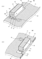
- FIG. 2A and 2B are perspective views of main parts of the antenna device 201 according to the first embodiment.
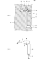
- 3A is a plan view of a main part of the antenna device 201, and
- FIG. 3B is an equivalent circuit diagram thereof.
- FIG. 4A shows the return loss characteristic during the direct power supply operation
- FIG. 4B shows the return loss characteristic during the capacity power supply operation.
- FIG. 5 is a diagram showing the current distribution and directivity of the substrate in the direct power feeding operation.
- FIG. 6 is a diagram showing the current distribution and directivity of the substrate in the capacity feeding operation.
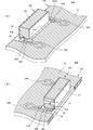
- FIGS. 7A and 7B are perspective views of the main part of the antenna device 202 according to the second embodiment.
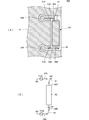
- FIG. 8A is a plan view of a main part of the antenna device 202, and FIG. 8B is an equivalent circuit diagram thereof.
- FIGS. 9A and 9B are perspective views of the main part of the antenna device 203 according to the third embodiment.
- FIG. 10A is a plan view of the main part of the antenna device 203, and FIG. 10B is an equivalent circuit diagram thereof.
- FIG. 11A is a plan view of the main part of the antenna device 204 according to the fourth embodiment, and FIG. 11B is an equivalent circuit diagram thereof.
- FIG. 12A is a plan view of the main part of the antenna device 205 according to the fifth embodiment, and FIG. 12B is an equivalent circuit diagram thereof.
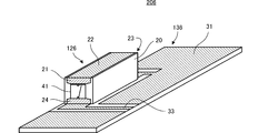
- FIG. 13 is a perspective view of a main part of an antenna device 206 according to the sixth embodiment.
- FIG. 14 is an equivalent circuit diagram of the antenna device 206.
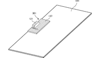
- FIG. 15 is a perspective view showing the antenna module 301 of the seventh embodiment and the mounting state of the antenna module 301.
- FIG. 16
- FIG. 2A and 2B are perspective views of main parts of the antenna device 201 according to the first embodiment. The viewpoint is different between FIG. 2A and FIG.
- the antenna device 201 includes a substrate 131 and an antenna chip 121 mounted on the substrate 131.
- a radiating electrode 21 is formed on the first end surface of the rectangular parallelepiped dielectric base 20, a radiating electrode 22 is formed on the upper surface, and a radiating electrode 23 is formed on the second end surface. These radiation electrodes 21, 22, and 23 are continuous.
- a capacitive power supply electrode 24 is formed on the first end face of the dielectric substrate 20. Mounting electrodes connected to the radiation electrodes 21 and 23 and the capacitive power supply electrode 24 are formed on the lower surface of the dielectric substrate 20.
- the antenna chip 121 is constituted by the dielectric substrate 20 and the various electrodes formed on the outer surface thereof.
- a ground electrode 31, a power supply circuit connection electrode 32, power supply lines 33, 34, 35, a tip electrode 36, and the like are formed on the upper surface of the base material 30.
- a substrate 131 is constituted by the base material 30 and the various electrodes formed on the base material 30.
- the antenna chip 121 is mounted on the non-ground region NGA where the ground electrode of the substrate 131 is not formed.
- the radiation electrode 21 is electrically connected to the power supply line 35, and the capacitive power supply electrode 24 is electrically connected to the power supply line 34.
- the radiation electrode 23 is electrically connected to the tip electrode 36.
- a first switch element 41 is connected (mounted) between the power supply line 33 and the power supply lines 34 and 35.
- a second switch element 42 is connected (mounted) between the tip electrode 36 and the ground electrode 31.
- a matching circuit 51 is connected between the power supply line 33 and the ground electrode 31 at a predetermined position.
- the power supply circuit connection electrode 32 is represented as a floating island pattern in order to clearly indicate the power supply line, but generally, a power supply circuit line (coplanar line) formed on the substrate 131 is connected. The same applies to other embodiments described later.
- the antenna chip 121 corresponds to a “radiating element” recited in the claims of the present invention.
- the lower end of the radiation electrode 21 is a direct feeding point PDF.
- the opposing portion (capacitance forming portion) between the capacitive power supply electrode 24 and the radiation electrode 21 is a capacitive power supply point Pcf.
- the lower end of the radiation electrode 23 is a ground point Pg.
- FIG. 3A is a plan view of the main part of the antenna device 201, and FIG. 3B is an equivalent circuit diagram thereof.
- the first switch element 41 shown in FIG. 3A selectively connects the power supply line 33 to one of the power supply lines 34 or 35. Further, the second switch element 42 switches between grounding / opening of the tip electrode 36.
- the radiation electrode RE corresponds to the radiation electrodes 21, 22, and 23.
- the power feeding capacity CF corresponds to the capacity of the capacity feeding point.
- the second switch element 42 When the first switch element 41 shown in FIGS. 3 (A) and 3 (B) selects the power supply line 34 side, the second switch element 42 is turned on. In this state, the radiation electrode RE is capacitively fed. On the contrary, when the first switch element 41 selects the power supply line 35 side, the second switch element 42 is opened. In this state, the radiation electrode RE is directly supplied with power.
- the first switch element 41 and the second switch element 42 are configured by PIN diodes (p-intrinsic-nodeDiode) or MESFETs (Metal Semiconductor Field Effect Transistor). Since these switch elements are small in shape, the area occupied by the antenna can be saved. Moreover, since the switching speed is fast, the antenna operation can be switched instantaneously. When high speed is not required for switching, a MEMS (Micro Electro Mechanical Systems) element may be used. Control signals for these switch elements are given from a control circuit (not shown) formed on the substrate 131. The same applies to other embodiments described later.
- FIG. 4A shows the return loss characteristic during the direct power supply operation
- FIG. 4B shows the return loss characteristic during the capacity power supply operation.
- the resonance frequency of the radiation electrode of the antenna chip 121 is a frequency in the 1.5 GHz band. In any power feeding operation, the return loss at the same frequency is ⁇ 10 dB or less in the operating frequency band, and it can be seen that sufficient return loss characteristics can be obtained.
- FIG. 5 is a diagram showing the current distribution and directivity of the substrate in the direct power supply operation
- FIG. 6 is a diagram showing the current distribution and directivity of the substrate in the capacitive power supply operation
- FIGS. 5A and 6A are diagrams showing the intensity distribution of the current flowing through the ground electrode 31 of the substrate 131 (the density distribution of the substrate current). The higher the current density, the higher the density.
- the substrate is disposed on the xy plane, and the mounting position of the antenna chip 121 is directed to the x-axis direction with respect to the substrate. In this example, the antenna chip 121 is mounted at a substantially central position on the long side of the substrate 131.
- FIGS. 5B and 6B are directivities on the xy plane (substrate surface direction) of the substrate, and FIGS. 5C and 6C are yz surfaces of the substrate (on the substrate). Directivity in a plane perpendicular to the surface). In both cases, the higher the radiation efficiency, the higher the concentration.
- the current density of the substrate current is different between the direct feeding operation and the capacitive feeding operation.
- the current density of the side SF of the substrate 131 on which the antenna chip 121 is mounted is high in both the direct feeding operation and the capacitive feeding conductor, in the direct feeding operation, the current in the side SC orthogonal to the side SF on which the antenna chip 121 is mounted. The density also tends to increase.
- a current is widely distributed on the side SF of the substrate 131 along the mounting position of the antenna chip 121.
- the antenna directivity is directed toward the side where the substrate current density is high. Therefore, the direct power supply operation is directed in the x direction, and the capacitive power supply operation is directed in the y direction.
- the directivity diagrams of FIGS. 5B, 5C, 6B, and 6C That is, in the direct power feeding operation, as shown in FIG. 5B and FIG. 5C, the direction in which the radiated electric field intensity is high is substantially in the y-axis direction. In the capacitive power supply operation, as shown in FIGS. 6B and 6C, the direction in which the radiated electric field intensity is high is substantially in the x-axis direction.
- the antenna device Since the switching between the direct power feeding operation and the capacitive power feeding operation is performed by switching between the first switch element 41 and the second switch element 42, the antenna device is switched by switching between the first switch element 41 and the second switch element 42.
- the directivity of 201 can be switched.
- FIGS. 7A and 7B are perspective views of the main part of the antenna device 202 according to the second embodiment. 7A and FIG. 7B have different viewpoints.
- the antenna device 202 includes a substrate 132 and an antenna chip 122 mounted on the substrate 132.
- a radiating electrode 21 is formed on the first end surface of the rectangular parallelepiped dielectric base 20, a radiating electrode 22 is formed on the upper surface, and a radiating electrode 23 is formed on the second end surface. These radiation electrodes 21, 22, and 23 are continuous.
- a capacitive power supply electrode 24 is formed on the first end face of the dielectric substrate 20.
- a mounting electrode connected to the radiation electrode 23 and the capacitive power supply electrode 24 is formed on the lower surface of the dielectric substrate 20.
- the antenna chip 122 is composed of the dielectric base 20 and various electrodes formed on the outer surface thereof.
- a ground electrode 31, a power supply circuit connection electrode 32, power supply lines 33, 34, 35, a tip electrode 36, and the like are formed on the upper surface of the base material 30.
- a substrate 132 is configured by the base material 30 and the above-described various electrodes formed on the base material 30.
- the antenna chip 122 is mounted on the non-ground region NGA where the ground electrode of the substrate 132 is not formed.
- the radiation electrode 23 is electrically connected to the power supply line 35, and the capacitive power supply electrode 24 is electrically connected to the power supply line 34.
- the radiation electrode 23 is electrically connected to the tip electrode 36.
- a first switch element 41 is connected (mounted) between the power supply line 33 and the power supply lines 34 and 35.
- a second switch element 42 is connected (mounted) between the tip electrode 36 and the ground electrode 31.
- a matching circuit 51 is connected between the power supply line 33 and the ground electrode 31 at a predetermined position.
- the antenna chip 122 corresponds to a “radiating element” recited in the claims of the present invention.
- the opposing portion (capacitance forming portion) between the capacitive power supply electrode 24 and the radiation electrode 21 is a capacitive power supply point Pcf.
- the lower end of the radiation electrode 23 is a connection point Pdg that is a direct feeding point or a grounding point.
- FIG. 8A is a plan view of the main part of the antenna device 202
- FIG. 8B is an equivalent circuit diagram thereof.
- the first switch element 41 shown in FIG. 8A selectively connects the power supply line 33 to one of the power supply lines 34 or 35. Further, the second switch element 42 switches between grounding / opening of the tip electrode 36.
- the radiation electrode RE corresponds to the radiation electrodes 21, 22, and 23.
- the power feeding capacity CF corresponds to the capacity of the capacity feeding point.
- the second switch element 42 When the first switch element 41 shown in FIGS. 8A and 8B selects the power supply line 34 side, the second switch element 42 is turned on. In this state, the radiation electrode RE is capacitively fed. On the contrary, when the first switch element 41 selects the power supply line 35 side, the second switch element 42 is opened. In this state, the radiation electrode RE is directly supplied with power.
- the first switch element 41 and the second switch element 42 since the direct power feeding operation and the capacitive power feeding operation are switched by switching the first switch element 41 and the second switch element 42, the first switch element 41 and the second switch element 41 The directivity of the antenna device 202 can be switched by switching the switch element 42.
- FIGS. 9A and 9B are perspective views of the main part of the antenna device 203 according to the third embodiment. The viewpoint is different between FIG. 9A and FIG.
- the antenna device 203 includes a substrate 133 and an antenna chip 123 mounted on the substrate 133.
- a radiating electrode 21 is formed on the first end surface of the rectangular parallelepiped dielectric base 20, a radiating electrode 22 is formed on the upper surface, and a radiating electrode 23 is formed on the second end surface. These radiation electrodes 21, 22, and 23 are continuous.
- a capacitive power supply electrode 24 is formed on the first end face of the dielectric substrate 20.
- a mounting electrode connected to the radiation electrode 23 and the capacitive power supply electrode 24 is formed on the lower surface of the dielectric substrate 20.
- the antenna chip 123 is constituted by the dielectric base 20 and the various electrodes formed on the outer surface thereof.
- a ground electrode 31, power supply circuit connection electrodes 32A and 32B, power supply lines 33A and 33B, tip electrodes 36A and 36B, and the like are formed on the upper surface of the base material 30.
- a substrate 133 is constituted by the base material 30 and the above-described various electrodes formed on the base material 30.
- the antenna chip 123 is mounted on the non-ground region NGA where the ground electrode of the substrate 133 is not formed.
- the radiation electrode 23 is electrically connected to the tip electrode 36A, and the capacitive power supply electrode 24 is electrically connected to the tip electrode 36B.
- a first switch element 41 is connected (mounted) to the tip electrode 36 ⁇ / b> A, the power supply line 33 ⁇ / b> A, and the ground electrode 31.
- a second switch element 42 is connected (mounted) between the feed line 33B and the tip electrode 36B.
- Matching circuits 51A and 51B are connected to the ground electrode 31 at predetermined positions of the power supply lines 33A and 33B, respectively.
- the antenna chip 123 corresponds to a “radiating element” described in the claims of the present invention.
- the opposing portion (capacitance forming portion) between the capacitive power supply electrode 24 and the radiation electrode 21 is a capacitive power supply point Pcf.
- the lower end of the radiation electrode 23 is a connection point Pdg that is a direct feeding point or a grounding point.
- FIG. 10A is a plan view of the main part of the antenna device 203, and FIG. 10B is an equivalent circuit diagram thereof.
- the first switch element 41 shown in FIG. 10A selectively connects the tip electrode 36A to one of the feed line 33A and the ground electrode.
- the second switch element 42 switches whether the tip electrode 36B is connected to the power supply line 33B or opened.
- the radiation electrode RE corresponds to the radiation electrodes 21, 22, and 23.
- the power feeding capacity CF corresponds to the capacity of the capacity feeding point.
- the direct power feeding operation and the capacitive power feeding operation are switched by switching the first switch element 41 and the second switch element 42, the first switch element 41 and the second switch element 41
- the directivity of the antenna device 201 can be switched by switching the switch element 42.
- the power feeding from the two power feeding circuits is switched by switching the first switch element 41 and the second switch element 42, the direct power feeding operation and the capacity power feeding operation can be fed by separate power feeding circuits.
- FIG. 11A is a plan view of the main part of the antenna device 204 according to the fourth embodiment, and FIG. 11B is an equivalent circuit diagram thereof.
- the antenna device 204 includes a substrate 134 and an antenna chip 121 mounted on the substrate 134. This antenna chip 121 is the same as the antenna chip shown in the first embodiment.
- a switching matching circuit 52 is connected to the ground electrode 31 at a predetermined position of the power supply line 33 provided on the substrate 134.
- the switching matching circuit 52 includes a plurality (two in this example) of matching circuit elements 52a and 52b and a third switch element 43.
- the third switch element 43 By switching the third switch element 43, one of the matching circuit elements 52a and 52b is connected between the feed line 33 and the ground.
- These matching circuit elements 52a and 52b are selected according to direct feeding and capacitive feeding to the radiation electrode RE. That is, the third switch element 43 is switched in conjunction with the switching of the first switch element 41 and the second switch element 42.
- FIG. 12A is a plan view of the main part of the antenna device 205 according to the fifth embodiment, and FIG. 12B is an equivalent circuit diagram thereof.
- the antenna device 205 includes a substrate 135 and an antenna chip 122 mounted on the substrate 135. This antenna chip 122 is the same as the antenna chip shown in the second embodiment.
- a switching matching circuit 52 is connected to the ground electrode 31 at a predetermined position of the power supply line 33 provided on the substrate 135.
- the switching matching circuit 52 includes matching circuit elements 52a and 52b and a third switch element 43.
- one of the matching circuit elements 52a and 52b is connected between the power supply line 33 and the ground by switching the third switch element 43.
- These matching circuit elements 52a and 52b are selected according to direct feeding and capacitive feeding to the radiation electrode RE. That is, the third switch element 43 is switched in conjunction with the switching of the first switch element 41 and the second switch element 42.
- FIG. 13 is a perspective view of a main part of an antenna device 206 according to the sixth embodiment.
- the antenna device 206 includes a substrate 136 and an antenna chip 126 mounted on the substrate 136.
- a radiating electrode 21 is formed on the first end face of the rectangular parallelepiped dielectric substrate 20, a radiating electrode 22 is formed on the upper surface, and a radiating electrode 23 (hidden on the rear face in FIG. 13) is formed on the second end face. These radiation electrodes 21, 22, and 23 are continuous.
- a capacitive power supply electrode 24 is formed on the first end face of the dielectric substrate 20, and a first switch element 41 is provided between the capacitive power supply electrode 24 and the radiation electrode 21.
- An electrode connected to the ground electrode 31 of the substrate is formed on the second end face of the dielectric substrate 20, and a second switch element is provided between the electrode and the radiation electrode 23.
- a switch symbol is shown in the switch element 41 portion.
- FIG. 14 is an equivalent circuit diagram of the antenna device 206.
- the radiation electrode RE corresponds to the radiation electrodes 21, 22, and 23.
- the power feeding capacity CF corresponds to the capacity of the capacity feeding point.
- the first switch element 41 switches between conduction / opening at both ends of the power supply capacitor CF.
- the second switch element 42 switches between grounding / opening of the tip of the radiation electrode 23.
- the second switch element 42 When the first switch element 41 shown in FIGS. 13 and 14 is turned on, the second switch element 42 is opened. In this state, the radiation electrode RE is directly supplied with power. Conversely, when the first switch element 41 is opened, the second switch element 42 is brought into conduction. In this state, the radiation electrode RE is capacitively fed.
- the first switch element 41 and the second switch element 42 are provided in the antenna chip 126, the number of components mounted on the substrate 136 can be reduced and the whole can be simplified. Further, the space occupied by the antenna with respect to the substrate can be reduced.
- FIG. 15 is a perspective view showing the antenna module 301 of the seventh embodiment and the mounting state of the antenna module 301.
- the antenna module 301 is configured by configuring the antenna device shown in the first embodiment on a module substrate 137. On the lower surface of the module substrate 137, electrodes for mounting on the mounting destination substrate 141 are formed.
- the antenna device is configured by mounting the antenna module 301 on the substrate 141.
- FIG. 16 is a plan view of a mobile terminal according to the eighth embodiment.
- the portable terminal 411 is provided with a liquid crystal display panel LCD on the front surface of the housing 401.
- a housing 131 is provided inside the housing 401, and an antenna chip 121 is mounted on the substrate 131.
- the substrate 131 and the antenna chip 121 constitute the antenna device shown in the first embodiment.
- a communication circuit including a power feeding circuit for the antenna device is formed on the substrate 131.
- the antenna chip is configured by forming various electrodes on the dielectric substrate 20, but the antenna chip may be configured by forming various electrodes on the magnetic substrate. In either case, the antenna can be miniaturized because the electrode length can be designed short by the wavelength shortening effect.
- CF feeding capacity NGA ... non-ground region Pcf ... capacity feeding point PDF ... direct feeding point Pdg ... connection point Pg ... grounding point RE ... radiation electrode 20 ... dielectric substrates 21, 22, 23 ... radiation electrode 24 ... capacity feeding electrode 30 ... Substrate 31 ... Ground electrode 32 ... Feed circuit connection electrodes 32A, 32B ... Feed circuit connection electrodes 33, 34, 35 ... Feed line 33A, 33B ... Feed line 36 ... Tip electrodes 36A, 36B ... Tip electrode 41 ... First Switch element 42 ... Second switch element 43 ... Third switch element 51 ... Matching circuits 51A, 51B ... Matching circuit 52 ... Switching matching circuits 52a, 52b ...
Landscapes
- Engineering & Computer Science (AREA)
- Computer Networks & Wireless Communication (AREA)
- Physics & Mathematics (AREA)
- Electromagnetism (AREA)
- Variable-Direction Aerials And Aerial Arrays (AREA)
- Support Of Aerials (AREA)
- Details Of Aerials (AREA)
Abstract
Description
給電ラインから前記放射素子の直接給電点または前記容量給電点に対する給電を切り替える第1のスイッチと、
前記放射素子の接地点とグランドとの間に導通/非導通を切り替える第2のスイッチとを備える。
給電ラインから前記放射素子の直接給電点または前記容量給電点に対する給電を切り替える第1のスイッチと、
前記放射素子の前記接続点とグランドとの間に導通/非導通を切り替える第2のスイッチとを備える。
前記放射素子の前記第1の接続点と第1の給電ラインまたはグランドとの接続を切り替える第1のスイッチと、
前記放射素子の前記第2の接続点と第2の給電ラインの接続/開放を切り替える第2のスイッチとを備える。
図2(A)、図2(B)は第1の実施形態に係るアンテナ装置201の主要部の斜視図である。図2(A)と図2(B)とでは視点が異なる。アンテナ装置201は基板131と基板131に実装されたアンテナチップ121とで構成されている。
給電ライン33と給電ライン34,35との間には第1のスイッチ素子41が接続(実装)されている。先端電極36とグランド電極31との間には第2のスイッチ素子42が接続(実装)されている。給電ライン33の所定位置にはグランド電極31との間に整合回路51が接続されている。
図7(A)、図7(B)は第2の実施形態に係るアンテナ装置202の主要部の斜視図である。図7(A)と図7(B)とでは視点が異なる。アンテナ装置202は基板132と基板132に実装されたアンテナチップ122とで構成されている。
給電ライン33と給電ライン34,35との間には第1のスイッチ素子41が接続(実装)されている。先端電極36とグランド電極31との間には第2のスイッチ素子42が接続(実装)されている。給電ライン33の所定位置にはグランド電極31との間に整合回路51が接続されている。
図9(A)、図9(B)は第3の実施形態に係るアンテナ装置203の主要部の斜視図である。図9(A)と図9(B)とでは視点が異なる。アンテナ装置203は基板133と基板133に実装されたアンテナチップ123とで構成されている。
先端電極36A、給電ライン33Aおよびグランド電極31には第1のスイッチ素子41が接続(実装)されている。給電ライン33Bと先端電極36Bとの間には第2のスイッチ素子42が接続(実装)されている。給電ライン33A,33Bの所定位置にはグランド電極31との間に整合回路51A,51Bがそれぞれ接続されている。
図11(A)は第4の実施形態に係るアンテナ装置204の主要部の平面図、図11(B)はその等価回路図である。アンテナ装置204は基板134と基板134に実装されたアンテナチップ121とで構成されている。このアンテナチップ121は第1の実施形態で示したアンテナチップと同じものである。基板134に設けられている給電ライン33の所定位置にはグランド電極31との間に切替整合回路52が接続されている。
図12(A)は第5の実施形態に係るアンテナ装置205の主要部の平面図、図12(B)はその等価回路図である。アンテナ装置205は基板135と基板135に実装されたアンテナチップ122とで構成されている。このアンテナチップ122は第2の実施形態で示したアンテナチップと同じものである。基板135に設けられている給電ライン33の所定位置にはグランド電極31との間に切替整合回路52が接続されている。
図13は第6の実施形態に係るアンテナ装置206の主要部の斜視図である。アンテナ装置206は基板136と基板136に実装されたアンテナチップ126とで構成されている。
なお、図13ではスイッチ素子41部分にスイッチ記号を表している。
図15は第7の実施形態のアンテナモジュール301およびアンテナモジュール301の実装状態を示す斜視図である。このアンテナモジュール301は、モジュール基板137に第1の実施形態で示したアンテナ装置が構成されたものである。モジュール基板137の下面には実装先基板141への実装用電極が形成されている。アンテナモジュール301が基板141に実装されることによってアンテナ装置が構成される。
図16は第8の実施形態の携帯端末の平面図である。携帯端末411は筐体401の前面に液晶表示パネルLCDが設けられている。筐体401の内部には基板131を備えていて、この基板131にアンテナチップ121が実装されている。この基板131とアンテナチップ121とによって第1の実施形態で示したアンテナ装置が構成されている。基板131にはアンテナ装置に対する給電回路を含む通信回路が構成されている。
以上に示した各実施形態では誘電体基体20に各種電極を形成してアンテナチップを構成したが、磁性体基体に各種電極を形成することによってアンテナチップを構成してもよい。いずれの場合でも波長短縮効果によって電極長を短く設計できることから、アンテナを小型化できる。
NGA…非グランド領域
Pcf…容量給電点
Pdf…直接給電点
Pdg…接続点
Pg…接地点
RE…放射電極
20…誘電体基体
21,22,23…放射電極
24…容量給電電極
30…基材
31…グランド電極
32…給電回路接続電極
32A,32B…給電回路接続電極
33,34,35…給電ライン
33A,33B…給電ライン
36…先端電極
36A,36B…先端電極
41…第1のスイッチ素子
42…第2のスイッチ素子
43…第3のスイッチ素子
51…整合回路
51A,51B…整合回路
52…切替整合回路
52a,52b…整合回路素子
121~123,126…アンテナチップ
131~136…基板
137…モジュール基板
141…基板
201~206…アンテナ装置
301…アンテナモジュール
401…筐体
411…携帯端末
Claims (11)
- 直接給電点、容量給電点および接地点を備える放射素子と、
給電ラインから前記放射素子の直接給電点または前記容量給電点に対する給電を切り替える第1のスイッチと、
前記放射素子の接地点とグランドとの間に導通/非導通を切り替える第2のスイッチとを備えたことを特徴とするアンテナ装置。 - 直接給電点または接地点となる接続点と容量給電点とを備える放射素子と、
給電ラインから前記放射素子の直接給電点または前記容量給電点に対する給電を切り替える第1のスイッチと、
前記放射素子の前記接続点とグランドとの間に導通/非導通を切り替える第2のスイッチとを備えたことを特徴とするアンテナ装置。 - 直接給電点または接地点となる第1の接続点と容量給電点となる第2の接続点とを備える放射素子と、
前記放射素子の前記第1の接続点と第1の給電ラインまたはグランドとの接続を切り替える第1のスイッチと、
前記放射素子の前記第2の接続点と第2の給電ラインの接続/開放を切り替える第2のスイッチとを備えたことを特徴とするアンテナ装置。 - 前記第1のスイッチまたは第2のスイッチの少なくとも一方はPINダイオードまたはMESFETで構成されている、請求項1~3のいずれかに記載のアンテナ装置。
- 前記給電ラインにインピーダンス整合回路が配置された、請求項1~4のいずれかに記載のアンテナ装置。
- 前記給電ラインに対する前記インピーダンス整合回路の接続を切り替える第3のスイッチを備えた、請求項5に記載のアンテナ装置。
- 前記第3のスイッチはPINダイオードまたはMESFETで構成されている、請求項6に記載のアンテナ装置。
- 前記放射素子は直方体形状の誘電体または磁性体の基体に放射電極が形成されたものである、請求項1~7のいずれかに記載のアンテナ装置。
- 前記基体に前記第1のスイッチまたは第2のスイッチが設けられた、請求項8に記載のアンテナ装置。
- 請求項5~7のいずれかに記載のアンテナ装置を備え、当該アンテナ装置の少なくとも前記放射素子、前記第1のスイッチ、前記第2のスイッチ、および前記インピーダンス整合回路は一つの基板に構成され、実装先基板への実装用電極が前記基板に形成されたアンテナモジュール。
- 請求項1~9のいずれかに記載のアンテナ装置または請求項10に記載のアンテナモジュールと、前記アンテナ装置またはアンテナモジュールに給電する給電回路とを備えた携帯端末。
Priority Applications (3)
| Application Number | Priority Date | Filing Date | Title |
|---|---|---|---|
| JP2012532406A JP5418688B2 (ja) | 2010-12-21 | 2011-12-16 | アンテナ装置、アンテナモジュールおよび携帯端末 |
| CN201180039913.9A CN103069646B (zh) | 2010-12-21 | 2011-12-16 | 天线装置、天线模块及便携终端 |
| US13/762,277 US9054407B2 (en) | 2010-12-21 | 2013-02-07 | Antenna device, antenna module, and portable terminal |
Applications Claiming Priority (2)
| Application Number | Priority Date | Filing Date | Title |
|---|---|---|---|
| JP2010284214 | 2010-12-21 | ||
| JP2010-284214 | 2010-12-21 |
Related Child Applications (1)
| Application Number | Title | Priority Date | Filing Date |
|---|---|---|---|
| US13/762,277 Continuation US9054407B2 (en) | 2010-12-21 | 2013-02-07 | Antenna device, antenna module, and portable terminal |
Publications (1)
| Publication Number | Publication Date |
|---|---|
| WO2012086530A1 true WO2012086530A1 (ja) | 2012-06-28 |
Family
ID=46313803
Family Applications (1)
| Application Number | Title | Priority Date | Filing Date |
|---|---|---|---|
| PCT/JP2011/079136 Ceased WO2012086530A1 (ja) | 2010-12-21 | 2011-12-16 | アンテナ装置、アンテナモジュールおよび携帯端末 |
Country Status (4)
| Country | Link |
|---|---|
| US (1) | US9054407B2 (ja) |
| JP (1) | JP5418688B2 (ja) |
| CN (1) | CN103069646B (ja) |
| WO (1) | WO2012086530A1 (ja) |
Cited By (1)
| Publication number | Priority date | Publication date | Assignee | Title |
|---|---|---|---|---|
| JP2015130655A (ja) * | 2013-12-31 | 2015-07-16 | 群▲マイ▼通訊股▲ふん▼有限公司 | アンテナ構造及びこれを用いた無線通信装置 |
Families Citing this family (3)
| Publication number | Priority date | Publication date | Assignee | Title |
|---|---|---|---|---|
| TWI549369B (zh) * | 2013-12-26 | 2016-09-11 | 宏碁股份有限公司 | 通訊裝置 |
| CN110710055B (zh) * | 2017-06-27 | 2020-12-25 | 株式会社村田制作所 | 支持双频段天线装置 |
| TWI841002B (zh) * | 2022-10-17 | 2024-05-01 | 華碩電腦股份有限公司 | 天線結構 |
Citations (5)
| Publication number | Priority date | Publication date | Assignee | Title |
|---|---|---|---|---|
| JPH11112226A (ja) * | 1997-09-30 | 1999-04-23 | Kokusai Electric Co Ltd | 偏波面切替えアンテナ |
| JP2004165965A (ja) * | 2002-11-13 | 2004-06-10 | Murata Mfg Co Ltd | 面実装型アンテナおよびその製造方法および通信装置 |
| JP2005020368A (ja) * | 2003-06-26 | 2005-01-20 | Nippon Telegr & Teleph Corp <Ntt> | マルチビームアンテナ |
| JP2008118535A (ja) * | 2006-11-07 | 2008-05-22 | Murata Mfg Co Ltd | アンテナ構造およびそれを備えた無線通信装置 |
| JP2008167421A (ja) * | 2006-12-05 | 2008-07-17 | Matsushita Electric Ind Co Ltd | アンテナ装置及び無線通信装置 |
Family Cites Families (10)
| Publication number | Priority date | Publication date | Assignee | Title |
|---|---|---|---|---|
| JP3159084B2 (ja) | 1995-09-28 | 2001-04-23 | 株式会社村田製作所 | 表面実装型アンテナおよびこれを用いた通信機 |
| JP2000114856A (ja) * | 1998-09-30 | 2000-04-21 | Nec Saitama Ltd | 逆fアンテナおよびそれを用いた無線装置 |
| WO2001029927A1 (de) * | 1999-10-15 | 2001-04-26 | Siemens Aktiengesellschaft | Schaltbare antenne |
| JP2001326514A (ja) | 2000-05-18 | 2001-11-22 | Sharp Corp | 携帯無線機用アンテナ |
| EP1335449A1 (en) * | 2000-10-31 | 2003-08-13 | Mitsubishi Denki Kabushiki Kaisha | Antenna device and portable machine |
| JP2005150937A (ja) * | 2003-11-12 | 2005-06-09 | Murata Mfg Co Ltd | アンテナ構造およびそれを備えた通信機 |
| JP3889423B2 (ja) | 2004-12-16 | 2007-03-07 | 松下電器産業株式会社 | 偏波切り替えアンテナ装置 |
| EP2048739A4 (en) * | 2006-07-28 | 2009-08-05 | Murata Manufacturing Co | ANTENNA DEVICE AND RADIO COMMUNICATION DEVICE |
| FI120427B (fi) * | 2007-08-30 | 2009-10-15 | Pulse Finland Oy | Säädettävä monikaista-antenni |
| CN101436710B (zh) * | 2007-11-14 | 2012-12-19 | 深圳富泰宏精密工业有限公司 | 指向性天线以及装设指向性天线的携带型电子装置 |
-
2011
- 2011-12-16 WO PCT/JP2011/079136 patent/WO2012086530A1/ja not_active Ceased
- 2011-12-16 CN CN201180039913.9A patent/CN103069646B/zh not_active Expired - Fee Related
- 2011-12-16 JP JP2012532406A patent/JP5418688B2/ja not_active Expired - Fee Related
-
2013
- 2013-02-07 US US13/762,277 patent/US9054407B2/en not_active Expired - Fee Related
Patent Citations (5)
| Publication number | Priority date | Publication date | Assignee | Title |
|---|---|---|---|---|
| JPH11112226A (ja) * | 1997-09-30 | 1999-04-23 | Kokusai Electric Co Ltd | 偏波面切替えアンテナ |
| JP2004165965A (ja) * | 2002-11-13 | 2004-06-10 | Murata Mfg Co Ltd | 面実装型アンテナおよびその製造方法および通信装置 |
| JP2005020368A (ja) * | 2003-06-26 | 2005-01-20 | Nippon Telegr & Teleph Corp <Ntt> | マルチビームアンテナ |
| JP2008118535A (ja) * | 2006-11-07 | 2008-05-22 | Murata Mfg Co Ltd | アンテナ構造およびそれを備えた無線通信装置 |
| JP2008167421A (ja) * | 2006-12-05 | 2008-07-17 | Matsushita Electric Ind Co Ltd | アンテナ装置及び無線通信装置 |
Cited By (1)
| Publication number | Priority date | Publication date | Assignee | Title |
|---|---|---|---|---|
| JP2015130655A (ja) * | 2013-12-31 | 2015-07-16 | 群▲マイ▼通訊股▲ふん▼有限公司 | アンテナ構造及びこれを用いた無線通信装置 |
Also Published As
| Publication number | Publication date |
|---|---|
| US20130147674A1 (en) | 2013-06-13 |
| JP5418688B2 (ja) | 2014-02-19 |
| JPWO2012086530A1 (ja) | 2014-05-22 |
| US9054407B2 (en) | 2015-06-09 |
| CN103069646A (zh) | 2013-04-24 |
| CN103069646B (zh) | 2015-06-24 |
Similar Documents
| Publication | Publication Date | Title |
|---|---|---|
| CN110970728B (zh) | 具有天线模块隔离结构的电子设备 | |
| US8604994B2 (en) | Antenna apparatus including feeding elements and parasitic elements activated as reflectors | |
| KR101982641B1 (ko) | 3개의 편극 신호에 대한 안테나 소자 | |
| CN106711578B (zh) | 多频段天线 | |
| US9660340B2 (en) | Multiband antenna | |
| CN102800967B (zh) | 无线终端装置用的天线 | |
| JP5794312B2 (ja) | アンテナ装置および電子機器 | |
| JP2007081712A (ja) | 携帯無線機およびアンテナ装置 | |
| JP5093230B2 (ja) | アンテナおよび無線通信機 | |
| CN106129613A (zh) | 可调辐射场型的天线结构 | |
| JPWO2004097980A1 (ja) | 広帯域平板状アンテナ | |
| KR20060094603A (ko) | 유전체 칩 안테나 | |
| JP5418688B2 (ja) | アンテナ装置、アンテナモジュールおよび携帯端末 | |
| US9564687B2 (en) | Directive antenna apparatus mounted on a board | |
| JP5422587B2 (ja) | アンテナ装置 | |
| US20130021210A1 (en) | Wireless communication apparatus | |
| US6618015B2 (en) | Antenna for use with radio device | |
| JP7425554B2 (ja) | アンテナ装置 | |
| JP3981678B2 (ja) | 自己補対アンテナ装置 | |
| US20140347250A1 (en) | Antenna apparatus | |
| CN222705819U (zh) | 天线结构 | |
| KR100866221B1 (ko) | 평면형 인버티드 에프 안테나 | |
| Kayat et al. | Frequency reconfigurable truncated rhombuslike slotted antenna with patch size reduction | |
| JP2006246228A (ja) | アンテナ装置および無線通信システム | |
| JP2006197188A (ja) | アンテナ |
Legal Events
| Date | Code | Title | Description |
|---|---|---|---|
| WWE | Wipo information: entry into national phase |
Ref document number: 201180039913.9 Country of ref document: CN |
|
| WWE | Wipo information: entry into national phase |
Ref document number: 2012532406 Country of ref document: JP |
|
| 121 | Ep: the epo has been informed by wipo that ep was designated in this application |
Ref document number: 11851662 Country of ref document: EP Kind code of ref document: A1 |
|
| NENP | Non-entry into the national phase |
Ref country code: DE |
|
| 122 | Ep: pct application non-entry in european phase |
Ref document number: 11851662 Country of ref document: EP Kind code of ref document: A1 |