WO2012081473A1 - 入力システム - Google Patents
入力システム Download PDFInfo
- Publication number
- WO2012081473A1 WO2012081473A1 PCT/JP2011/078322 JP2011078322W WO2012081473A1 WO 2012081473 A1 WO2012081473 A1 WO 2012081473A1 JP 2011078322 W JP2011078322 W JP 2011078322W WO 2012081473 A1 WO2012081473 A1 WO 2012081473A1
- Authority
- WO
- WIPO (PCT)
- Prior art keywords
- input
- light
- input device
- control signal
- pen
- Prior art date
- Legal status (The legal status is an assumption and is not a legal conclusion. Google has not performed a legal analysis and makes no representation as to the accuracy of the status listed.)
- Ceased
Links
Images






Classifications
-
- G—PHYSICS
- G06—COMPUTING OR CALCULATING; COUNTING
- G06F—ELECTRIC DIGITAL DATA PROCESSING
- G06F3/00—Input arrangements for transferring data to be processed into a form capable of being handled by the computer; Output arrangements for transferring data from processing unit to output unit, e.g. interface arrangements
- G06F3/01—Input arrangements or combined input and output arrangements for interaction between user and computer
- G06F3/03—Arrangements for converting the position or the displacement of a member into a coded form
- G06F3/033—Pointing devices displaced or positioned by the user, e.g. mice, trackballs, pens or joysticks; Accessories therefor
- G06F3/0354—Pointing devices displaced or positioned by the user, e.g. mice, trackballs, pens or joysticks; Accessories therefor with detection of two-dimensional [2D] relative movements between the device, or an operating part thereof, and a plane or surface, e.g. 2D mice, trackballs, pens or pucks
- G06F3/03542—Light pens for emitting or receiving light
-
- G—PHYSICS
- G06—COMPUTING OR CALCULATING; COUNTING
- G06F—ELECTRIC DIGITAL DATA PROCESSING
- G06F3/00—Input arrangements for transferring data to be processed into a form capable of being handled by the computer; Output arrangements for transferring data from processing unit to output unit, e.g. interface arrangements
- G06F3/01—Input arrangements or combined input and output arrangements for interaction between user and computer
- G06F3/03—Arrangements for converting the position or the displacement of a member into a coded form
- G06F3/033—Pointing devices displaced or positioned by the user, e.g. mice, trackballs, pens or joysticks; Accessories therefor
- G06F3/0354—Pointing devices displaced or positioned by the user, e.g. mice, trackballs, pens or joysticks; Accessories therefor with detection of two-dimensional [2D] relative movements between the device, or an operating part thereof, and a plane or surface, e.g. 2D mice, trackballs, pens or pucks
- G06F3/03545—Pens or stylus
-
- G—PHYSICS
- G06—COMPUTING OR CALCULATING; COUNTING
- G06F—ELECTRIC DIGITAL DATA PROCESSING
- G06F3/00—Input arrangements for transferring data to be processed into a form capable of being handled by the computer; Output arrangements for transferring data from processing unit to output unit, e.g. interface arrangements
- G06F3/01—Input arrangements or combined input and output arrangements for interaction between user and computer
- G06F3/03—Arrangements for converting the position or the displacement of a member into a coded form
- G06F3/033—Pointing devices displaced or positioned by the user, e.g. mice, trackballs, pens or joysticks; Accessories therefor
- G06F3/038—Control and interface arrangements therefor, e.g. drivers or device-embedded control circuitry
- G06F3/0386—Control and interface arrangements therefor, e.g. drivers or device-embedded control circuitry for light pen
-
- G—PHYSICS
- G06—COMPUTING OR CALCULATING; COUNTING
- G06F—ELECTRIC DIGITAL DATA PROCESSING
- G06F3/00—Input arrangements for transferring data to be processed into a form capable of being handled by the computer; Output arrangements for transferring data from processing unit to output unit, e.g. interface arrangements
- G06F3/01—Input arrangements or combined input and output arrangements for interaction between user and computer
- G06F3/03—Arrangements for converting the position or the displacement of a member into a coded form
- G06F3/041—Digitisers, e.g. for touch screens or touch pads, characterised by the transducing means
- G06F3/0416—Control or interface arrangements specially adapted for digitisers
- G06F3/04166—Details of scanning methods, e.g. sampling time, grouping of sub areas or time sharing with display driving
-
- G—PHYSICS
- G06—COMPUTING OR CALCULATING; COUNTING
- G06F—ELECTRIC DIGITAL DATA PROCESSING
- G06F3/00—Input arrangements for transferring data to be processed into a form capable of being handled by the computer; Output arrangements for transferring data from processing unit to output unit, e.g. interface arrangements
- G06F3/01—Input arrangements or combined input and output arrangements for interaction between user and computer
- G06F3/03—Arrangements for converting the position or the displacement of a member into a coded form
- G06F3/041—Digitisers, e.g. for touch screens or touch pads, characterised by the transducing means
- G06F3/042—Digitisers, e.g. for touch screens or touch pads, characterised by the transducing means by opto-electronic means
-
- G—PHYSICS
- G06—COMPUTING OR CALCULATING; COUNTING
- G06F—ELECTRIC DIGITAL DATA PROCESSING
- G06F3/00—Input arrangements for transferring data to be processed into a form capable of being handled by the computer; Output arrangements for transferring data from processing unit to output unit, e.g. interface arrangements
- G06F3/01—Input arrangements or combined input and output arrangements for interaction between user and computer
- G06F3/03—Arrangements for converting the position or the displacement of a member into a coded form
- G06F3/041—Digitisers, e.g. for touch screens or touch pads, characterised by the transducing means
- G06F3/046—Digitisers, e.g. for touch screens or touch pads, characterised by the transducing means by electromagnetic means
Definitions
- the present invention relates to an input system that enables input using an indicator such as a pen, and more particularly to an input system that enables input from a plurality of locations.
- FIG. 11 includes a liquid crystal panel 140 and a backlight unit 150 including an infrared light source.
- the liquid crystal panel 140 includes an upper transparent substrate 141 including color filters RCF, GCF, BCF and a transparent window W formed in the same layer; a thin film transistor for selecting a pixel (hereinafter referred to as “TFT”).
- TFT thin film transistor for selecting a pixel
- IRTFT infrared sensing thin film transistor
- a plurality of data lines and a plurality of gate lines are orthogonal to each other, a plurality of driving voltage lines parallel to the gate lines, and a plurality of gate lines and driving voltage lines are orthogonal to each other.
- a lead outline is formed.
- a TFT for selecting a pixel is formed on the lower transparent substrate 142 at the intersection of the data line and the gate line, and an IR TFT is formed at the intersection of the drive voltage supply line and the lead-out line.
- a pixel electrode is formed.
- a TFT for selecting a pixel supplies a data voltage from the data line to the pixel electrode in accordance with a scan signal from the gate line.
- the IRTFT senses the amount of infrared light reflected through the upper transparent substrate 141 and the transparent window W at the touched point. Infrared light quantity detection signal is output through the lead-out line.
- infrared light is reflected from the contact surface and received by the IR TFT.
- the infrared light received by the IR TFT is subjected to digital signal processing, pattern analysis, etc. by a digital signal processing circuit.
- the coordinate value of the touched point is calculated, and a plurality of touched points are recognized by the digital signal processing circuit.
- the touch image of the touched point is displayed on the liquid crystal panel.
- the touch panel described in Patent Document 2 includes a lower electrode member 204 in which an electrode made of a transparent conductive film and a pair of parallel bus bars are formed on an upper surface of a transparent insulating base material 201, and a flexible touch panel.
- the lower electrode member 204 includes an electrode pattern 202L and a pair of bus bars 203L provided in the left area, and an electrode pattern 202R and a pair of bus bars 203R provided in the right area, and each divided pattern is connected via an extraction line 220.
- Patent Document 3 There is also a panel that can be operated by multi-touch like Patent Document 3.
- Japanese Patent Publication “JP 2008-83675 A Japanese Patent Publication “Japanese Patent Laid-Open No. 2010-26641 (Released on February 4, 2010)” Japanese Patent Publication “Japanese Unexamined Patent Application Publication No. 2010-9412 (published January 14, 2010)”
- Patent Documents 1 to 3 accurately detects each of the plurality of pens that are simultaneously input, such as inputting characters or drawing lines simultaneously. There are times when you can't.
- the present invention has been made in view of the above problems, and an object thereof is to provide an input system capable of drawing characters and lines using a plurality of pens simultaneously.
- An input system comprising a plurality of pointing devices and an input device configured to sense an input position by sensing input by the pointing tools,
- the input device is configured so that the input device senses in accordance with the input timing of each indicator by differentiating the input timing between the indicators.
- the input device is configured to detect that it is configured to detect that continuous input has been made by connecting input positions in order along the passage of time for each pointing tool. .
- the sensing timing is made different between the respective indicators, and the inputs of a plurality of indicators are sequentially repeated in accordance with the timings. At this point, input by other pointing devices is not sensed. That is, since only one indicator is sensed, noise (input by other indicators) can be excluded.
- the input system is as described above.
- An input system comprising a plurality of pointing devices and an input device configured to sense an input position by sensing input by the pointing tools,
- the input device is configured so that the input device senses in accordance with the input timing of each indicator by differentiating the input timing between the indicators.
- the input device is characterized in that for each pointing tool, the input positions are connected in order along the passage of time to detect that continuous input has been made.
- FIG. 1 is a block diagram showing the configuration of the input system of this embodiment.
- the input system according to the present invention can be applied as a touch sensor integrated input device, for example, as an input system having a touch sensor function (particularly a character input function). Further, it is also suitable for any electronic device having a touch sensor function (particularly a character input function).
- the input system 1a of this embodiment includes a light pen 2 (indicator) and an input device 3 having a backlight BL, as shown in FIG.
- the optical pen 2 includes a light emitting diode LED, a pressure element PIE, a control board 5, and an amplifier circuit AMP.
- the light pen 2 is provided with a battery 7 at the center of the pen, a control board 5 is provided on the pen base side of the battery 7, and a light emitting diode LED is disposed on the pen tip side of the battery 7.
- the pressure element PIE is arranged at the pen tip.
- the battery 7 is not particularly limited, and a conventionally known small battery can be used.
- the light emitting diode LED (light emitting element) emits light detected by the photosensor circuit SEi of the photosensor touch panel 6 provided in the input device 3. Light emission of the light emitting diode LED is controlled by a control board 5 described later and a recognition engine 10 provided in the input device 3.
- the pressure element PIE detects the pressure acting between the two when the tip of the optical pen 2 is pressed against the surface of the optical sensor touch panel 6 provided in the input device 3.
- the detection result by the pressure element PIE is input to the microcomputer MC-1 (pressure signal generation unit) of the control board 5 via the amplifier circuit AMP, and digitized to about 1024 gradations, for example, to generate a pressure signal.
- the pressure signal is input to the recognition engine 10 via the Bluetooth (registered trademark) communication circuit BT-1 and the Bluetooth (registered trademark) communication circuit BT-2 of the recognition engine 10 of the input device 3.
- the control board 5 includes a timing IC (TIC), a microcomputer MC-1, and a Bluetooth (registered trademark) communication circuit BT-1.
- TIC timing IC
- MC-1 microcomputer MC-1
- BT-1 Bluetooth (registered trademark) communication circuit
- Timing IC controls the light emission of the light emitting diode LED based on the detection result of the pressure element PIE and the control signal from the microcomputer MC-1. A driving method based on the timing IC will be described later.
- the microcomputer MC-1 receives a control signal sent from the recognition engine 10 via the Bluetooth (registered trademark) communication circuit BT-1 and the Bluetooth (registered trademark) communication circuit BT-2 of the recognition engine 10 of the input device 3. Together with the signal, it is sent to a timing IC (TIC) to control the timing of light emission of the light emitting diode LED.
- TIC timing IC
- the Bluetooth (registered trademark) communication circuit BT-1 performs wireless communication with the Bluetooth (registered trademark) communication circuit BT-2 provided in the input device 3.
- the Bluetooth (registered trademark) communication circuit BT-2 provided in the recognition engine 10 and the Bluetooth (registered trademark) communication circuit BT-1 provided on the control board 5 of the optical pen 2 are both Bluetooth (registered trademark). (Trademark), and well-known wireless communication devices such as ZigBee can be employed.
- the input device 3 includes a photosensor touch panel 6, a display control circuit DCS, a backlight BL, and a recognition engine 10 (control unit, output unit).
- the optical sensor touch panel 6 includes a display unit 8, a source driver SD, a gate driver GD, an optical sensor drive circuit LSD (output unit), and an optical sensor output circuit LOD (output unit).
- the display unit 8 includes a plurality of pixels Pj arranged in a matrix, a plurality of scanning signal lines Gj, a plurality of data signal lines SL, a plurality of photosensor circuits SEi arranged in a matrix, and a plurality of pixels.
- the configuration of the photosensor circuit SEi will be described later.
- Display control circuit DCS controls source driver SD, gate driver GD, photosensor drive circuit LSD, recognition engine 10, and backlight BL.
- the source driver SD drives the data signal line SL
- the gate driver GD drives the scanning signal line Gj.
- the optical sensor drive circuit LSD drives the clock signal line CLKi, the reset signal line RSTi, and the read signal line RWSi.
- the recognition engine 10 drives the optical sensor output circuit LOD connected to the optical sensor output line OUT.
- the recognition engine 10 includes a microcomputer MC-2, a logic unit LGC, a memory MRY, and a Bluetooth (registered trademark) communication circuit BT-2.
- a touch point (input position coordinates) is calculated by the microcomputer MC-2 and the logic unit LGC based on the sensor image sent from the plurality of photosensor output lines OUT to the recognition engine 10 via the photosensor output circuit LOD.
- the memory MRY stores a calibration image and is mainly used for preprocessing (correction) for recognizing the sensor image.
- the Bluetooth (registered trademark) communication circuit BT-2 provided in the recognition engine 10 wirelessly communicates with the Bluetooth (registered trademark) communication circuit BT-1 provided on the control board 5 of the optical pen 2 described above.
- the present invention uses a plurality of light pens 2 at the same time by differentiating the sensing timing among the light pens and sequentially sensing the inputs of the plurality of light pens in accordance with the timing. Another feature is that the input from each light pen can be accurately sensed to input characters and draw lines.
- the present invention can also use one or three or more optical pens.
- the display control circuit DCS generates a control signal representing the timing at which the input device 3 senses the sensing result of the photosensor circuit SEi via the photosensor output line OUT and the photosensor output circuit LOD.
- the control signal is a signal for controlling the timing of light emission of the optical pen 2 and the timing of sensing.
- a control signal is transmitted from the Bluetooth (registered trademark) communication circuit BT-2 provided in the recognition engine 10 to the Bluetooth (registered trademark) provided on the control board 5 of the optical pen 2.
- the data is transmitted to the communication circuit BT-1 and transmitted from the Bluetooth (registered trademark) communication circuit BT-1 to the microcomputer MC-1 provided on the control board 5.
- control signal sent to the microcomputer MC-1 on the control board 5 is used differently depending on each light pen 2. Therefore, in the following description, the two optical pens 2 will be described by distinguishing between the first optical pen 2 and the second optical pen 2.
- the microcomputer MC-1 of the first light pen 2 generates a synchronization signal that is synchronized only with an odd number of timings when the control signal is turned on, and sends the synchronization signal to a timing IC (TIC).
- TIC timing IC
- the microcomputer MC-1 when the pressure is detected by the pressure element PIE, the microcomputer MC-1 generates a pressure signal based on the detection result, and sends the pressure signal together with the synchronization signal to the timing IC (TIC).
- the timing IC that receives the synchronization signal and the pressure signal receives a digital signal indicating that the pressure element PIE is applying pressure to the input device 3, that is, when the pressure signal is on.
- the light emitting diode LED disposed at the tip of the first light pen 2 is driven to emit light.
- the optical sensor touch panel 6 performs a sensing operation.
- the microcomputer MC-1 of the second light pen 2 sends a synchronization signal synchronized with only the even-numbered control signal to the timing IC (TIC).
- TIC timing IC
- FIG. 3 is a circuit diagram showing a configuration of the photosensor circuit SEi provided in the photosensor touch panel 6 of FIG.
- the optical sensor circuit SEi includes a photodiode SPD, a transistor TRA, a capacitor C, and a transistor TRB.
- the anode of the photodiode SPD is connected to the reset signal line RSTi.
- the cathode of the photodiode SPD is connected to one electrode of the capacitor C and the control electrode of the transistor TRB via the transistor TRA, and the other electrode of the capacitor C is connected to the read signal line RWSi.
- the control electrode of the transistor TRA is connected to the clock signal line CLKi, one conduction electrode of the transistor TRB is connected to VDD, and the other conduction electrode is connected to the photosensor output line OUT.
- the photosensor output line OUT is connected to the photosensor output circuit LOD.
- FIG. 4 is a timing chart showing the driving method described above.
- FIG. 4 specifically shows how to synchronize the sensing and the first light pen 2 and the second light pen 2, and will be described again with reference to FIG.
- each photosensor circuit When each control signal is on, each photosensor circuit stores a charge corresponding to the amount of light in the capacitor C, and outputs a potential corresponding to the amount of charge accumulated at the moment when the control signal is turned off.
- the synchronization signal of the first light pen 2 is turned on in synchronization with only the odd-numbered control signal.
- the pressure element PIE built in the first optical pen 2 detects the pressure when the pen tip touches the screen, and the pressure signal is turned on.
- the first light pen 2 is set to emit light only when both the synchronization signal and the pressure signal are on. In FIG. 4, light is emitted only at the timings of 1, 3, and 5 of the control signal, and the coordinates of the first light pen 2 are output at this timing. In other words, even if the pressure signal of the first light pen 2 is on at the even-numbered control signal, the first light pen 2 does not emit light and no sensing is performed.
- the switching of the control signal between on and off is performed once within one frame period (1/60 seconds). However, if the sensitivity of the optical sensor is high and sensing is possible at high speed, the control signals on and off can be performed twice within one frame period, and the position coordinates of the two pens can be acquired within one frame period. Thus, a smoother display can be performed.
- the synchronization signal of the second light pen 2 is turned on in synchronization with only the even-numbered control signal.
- the pressure signal of the second light pen 2 is turned on.
- the coordinates of the second light pen 2 are output. In other words, even if the pressure signal of the second light pen 2 is on at odd numbers of the control signal, the second light pen 2 does not emit light and sensing is not performed.
- the coordinates of two pens can be output by a single touch type touch panel.
- coordinate output can be realized while specifying the pen in the same way if the synchronization signal of one light pen is turned on each time the control signal is turned on. can do.
- the reset operation is performed at the moment when the control signal turns from off to on. Charge accumulation is performed during the on period, and an output operation is performed at the moment when the on state is turned off.
- Modification 1 As a modification of the present embodiment, a method that does not use the pressure signal of the optical pen can be considered.
- the light pen 2 always emits light when the light pen control signal is turned on.
- the light emission amount of the optical pen may be adjusted to a level that can be sensed by the optical sensor circuit Sei when the pen tip is very close to the input device.
- Modification 2 In the present embodiment, light emission is used as an input method to the input device, but the present invention is not limited to this.
- a certain signal (corresponding to light in the case of an optical sensor) is emitted from an indicator such as a pen, and if it is a device that employs a type of mechanism that obtains a coordinate position by receiving it at the input device, it is a certain type.
- These signals may not be light.
- an electromagnetic induction method as described later may be used, and an infrared camera method may be employed.
- the input system of this embodiment can be mounted on an electronic device as described above.
- a display device as one embodiment is shown in FIG.
- FIG. 5 is a diagram showing a display device of a touch sensor (touch panel) type. As shown in FIG. 5, the display device 70 of the present embodiment is provided with an input system 1a.
- an operation button group 76 is provided in the vicinity of the input system 1a.
- the operation button group 76 includes a function button group for performing various settings and function switching of the display device 70.
- the display device 70 of the present embodiment is equipped with the input system 1a having the touch sensor function described above on the display unit. Therefore, for example, a part of the operation button group 76 described above can be operated by a touch sensor in the display unit instead of the button operation.
- the display device 70 may be equipped with a speaker, a microphone, an image sensor, and the like.
- An electronic blackboard can be given as another example of the electronic device.
- An electronic blackboard is a whiteboard capable of electronically converting drawn content, and is sometimes referred to as a copy boat.
- the sensing timing is made different between the light pens, and the input of a plurality of light pens is sequentially repeated in accordance with the timing.
- the time of detection since an input by another light pen is not detected, only an input by a certain light pen is sensed, and noise (input by another light pen) can be excluded.
- the sensing timing is based on the control signal and the pressure signal, it is not necessary for the optical pen to always emit light, and light can be emitted only when sensing. Therefore, power consumption related to input can be reduced as compared with the case where the optical pen is always held in a sensed state.
- the light pen may perform an input operation (receiving a control signal together with the pressure signal) only when there is an intention to input to the input device. That is, it is possible to prevent an input operation from occurring even though there is no intention to input to the input device.
- this configuration is adopted, no light is emitted when the optical pen is not pressed against the input device, that is, when there is no intention to input. Thereby, power consumption due to wasteful light emission can be saved. Further, when another light pen is detected as input, it is possible to avoid causing an erroneous input by emitting light in the vicinity thereof.
- the control signal sent from the recognition engine 10 is sent to the timing IC (TIC) via the wireless communication device, and the light emission timing of the light emitting diode LED is emitted. Is controlling.
- the backlight BL of the input device 3 includes the infrared light generation unit IRG. The infrared light is emitted at a desired timing, and the red light is emitted.
- the configuration is such that the light emission timing of the optical pen is controlled by allowing external light to be received by the optical pen.
- the backlight BL includes an infrared light generation unit IRG.
- the recognition engine 10 of the input device 3 ′ does not have the Bluetooth (registered trademark) communication circuit BT-2 configured in the first embodiment, and does not have a mechanism for sending a control signal to the optical pen.
- the display control circuit DCS of the input device 3 ′ controls the backlight BL including the source driver SD, the gate driver GD, the optical sensor driving circuit LSD, the recognition engine 10, and the infrared light generation unit IRG.
- a photodiode PD is arranged in the optical pen 2 ′ of the input system 1b of the present embodiment. Further, the control board 5 of the optical pen 2 ′ does not have the Bluetooth (registered trademark) communication circuit BT-1 configured in the first embodiment.
- the photodiode PD receives the infrared light IRL emitted from the infrared light generation unit IRG in the backlight BL provided in the input device 3 ′.
- the optical pen 2 ′ can receive (detect) the infrared light from the infrared light generation unit IRG in the backlight BL provided in the input device 3 by the photodiode PD.
- the detection result by the photodiode PD is input to the timing IC (TIC) through the amplifier circuit AMP.
- the microcomputer MC-1 provided on the control board 5 of the light pen 2 ′ controls the light emission of the light emitting diode LED based on the detection results of the photodiode PD and the pressure element PIE.
- the microcomputer MC-1 receives the detection result of the photodiode PD sent via the timing IC (TIC), and outputs a synchronization signal for synchronizing the light emission timing of the light emitting diode LED and the sensing timing to the timing IC. (TIC).
- the microcomputer MC-1 of the first light pen 2 ′ generates a synchronization signal that is synchronized only with the odd-numbered timing at which the light reception signal of the photodiode PD is turned on, and the synchronization signal is used as a timing IC (TIC). Send it out.
- the microcomputer MC-1 of the first light pen 2 When the pressure is detected by the pressure element PIE, the microcomputer MC-1 of the first light pen 2 'generates a pressure signal based on the detection result, and sends the pressure signal together with the synchronization signal to the timing IC (TIC). .
- the timing IC (TIC) that has received the synchronization signal and the pressure signal receives the digital signal indicating that the pressure element PIE is applying pressure to the input device 3, and the tip of the first light pen 2
- the light emitting diode LED arranged in the unit is driven to emit light.
- the microcomputer MC-1 of the second optical pen 2 ′ generates a synchronization signal that is synchronized only with the even-numbered light reception signal of the photodiode PD, and sends the synchronization signal to the timing IC (TIC).
- the method of driving the light emitting diode LED disposed at the tip of the second light pen 2 ′ to emit light is the same as that of the first light pen 2.
- the light emission of the optical pen 2 ′ and the sensing of input based on the light emission are synchronized as in the first embodiment described above.
- the sensing timing different for each light pen 2 ′, it is possible to accurately sense an input from any of the light pens 2 ′.
- the present invention is not limited to this, and changes in the magnetic field can be detected. It is also possible to use it. That is, it is also possible to provide a configuration in which a coil is provided in the input device 3 ′, a magnetic field is generated there, and the change is detected by the coil provided in the optical pen 2 ′. Thereby, it is possible to realize a configuration in which the optical pen 2 ′ emits light only when a change in the magnetic field is detected.
- a control signal is sent from the input device 3 to all the light pens 2, and each light pen 2 emits light at a predetermined timing based on the received control signal. ing.
- a plurality of light pens 2 communicate with each other to synchronize.
- the input device 3 ′ that generates the control signal does not have a configuration for sending the control signal to the light pen 2.
- the optical pen 2 has a Bluetooth (registered trademark) communication circuit BT that allows the optical pens 2 to communicate with each other wirelessly.
- FIG. 8 is a timing chart showing the driving method of the input system 1c of this embodiment.
- the synchronization signal between the first light pen 2 and the second light pen 2 is synchronized so that on and off are reversed. It is controlled.
- the on time of the synchronization signal of each light pen 2 is assumed to be equal to or longer than the time of one cycle of sensing (the time from the moment when sensing is turned on until the next time it is turned on).
- the time from when the synchronization signal (input control signal) of one of the light pens changes from on to off until the synchronization signal of the next light pen changes from off to on is from the one on time of the sensing control signal. Too long. Thereby, it is possible to realize a state in which only one light pen is shining during one sensing.
- the input timing from each of the light pens 2 ′ can be accurately adjusted by making the sensing timing different for each light pen 2 ′. Sensing is possible.
- an input device is configured to input light by using a light pen.
- the input system 1d of the present embodiment uses an electromagnetic pen 20 as means for inputting to the input device 3 ′′.
- the electromagnetic pen 20 includes a coil 22 and a Bluetooth (registered trademark) communication circuit BT.
- the coil 22 changes a magnetic field near the pen.
- the Bluetooth (registered trademark) communication circuit BT may be used to synchronize between the magnetic pens 20, or a Bluetooth (registered trademark) communication circuit is provided on the input device 3 ′′ side, and this is connected to the magnetic pen. You may communicate with 20 Bluetooth (trademark) communication circuits BT.
- the input device 3 ′′ side has a built-in coil 30 for detecting a change in the magnetic field, and the position of the pen can be obtained.
- the magnetic field from each electromagnetic pen 20 is controlled by the same method as in the first to third embodiments described above, so that the coordinates obtained on the input device 3 ′′ side belong to which electromagnetic pen. I understand.
- a method of synchronizing the timing of sensing and the timing of magnetic field change may use a control signal sent from the input device to the pointing tool (light pen) as in Embodiment 1 described above. As shown, the indicators may be synchronized with each other.
- an input device is configured to input light by using a light pen.
- the input system 1 e of the present embodiment uses a pen 21 that emits infrared light as means for inputting to the input device 33.
- the pen 21 incorporates an infrared light source that emits infrared light.
- the infrared light source emits infrared light from the tip of the pen.
- a plurality of infrared cameras 25a and 25b for receiving infrared light emitted from the pen 21 close to the screen are provided.
- the infrared cameras are arranged at at least two different points adjacent to the screen. Thereby, the coordinate position of one pen can be obtained by the principle of triangulation.
- the input system according to the present invention is as described above.
- An input system comprising a plurality of pointing devices and an input device configured to sense an input position by sensing input by the pointing tools,
- the input device is configured so that the input device senses in accordance with the input timing of each indicator by differentiating the input timing between the indicators.
- the input device is configured to detect that it is configured to detect that continuous input has been made by connecting input positions in order along the passage of time for each pointing tool. .
- the sensing timing is made different between the respective indicators, and the inputs of a plurality of indicators are sequentially repeated in accordance with the timings. At this point, input by other pointing devices is not sensed. That is, since only one indicator is sensed, noise (input by other indicators) can be excluded.
- the input device generates a control signal indicating the timing of sensing the input of the pointing tool, sends a control signal to each of the pointing tools, and senses the input of the pointing tool based on the control signal.
- an output unit to The indicator has a receiving unit that receives the control signal, and is configured to input to the input device based on the received control signal. It is preferable that each said indicator performs input to the said input device according to the said control signal at a mutually different timing.
- the pointing device is configured to input to the input device based on the control signal, for example, when the light pen is used as the pointing device, the light pen needs to always emit light. No light can be emitted only when sensing.
- the input device includes: a control unit that generates a control signal indicating timing for sensing the input of the pointing tool; a light source unit that emits infrared light based on the control signal; and the pointing tool based on the control signal. And an output unit for sensing input,
- the indicator is configured to receive the infrared light and generate a light reception signal, and to input to the input device based on the light reception signal, It is preferable that each said indicator performs the input to the said input device according to the said light reception signal at a mutually different timing.
- the pointing device can be configured to input to the input device only when infrared light as a control signal is sensed by the photodiode of the pointing device.
- the light pen When used as an indicator, the light pen need not always emit light, and can be emitted only when the photodiode of the indicator senses infrared light, that is, at the timing of sensing.
- the input device includes a control unit that generates a control signal indicating timing for sensing the input of the pointing tool, and an output unit that senses the input of the pointing tool based on the control signal.
- Each of the pointing devices is an input control signal for controlling the input so as to input to the input device at different timings, and the input control signal synchronized with the control signal is transmitted and received between the pointing devices. It is preferable that
- the pointing device is configured to input to the input device based on a control signal, for example, when a light pen is used as the pointing device, it is not necessary to always emit light, It can emit light only when it is sensed.
- a light pen when used as an indicator, light can be emitted only when the photodiode of the indicator senses infrared rays, that is, at the timing of sensing, without always emitting light.
- the indicator has a pressure signal generation unit that generates a pressure signal when sensing the pressure generated when the tip is pressed against the input device, It is preferable that the indicator has an essential condition that the pressure signal is generated as a condition for performing input to the input device.
- the generation of the pressure signal indicates that there is an intention to input to the input device, and only in that case (in response to the control signal) the indicator performs an input operation. Just do it. That is, it is possible to prevent an input operation from occurring even though there is no intention to input to the input device.
- the optical pen is used as an indicator
- this configuration if this configuration is adopted, no light is emitted when the optical pen is not pressed against the input device, that is, when there is no intention to input. Thereby, power consumption due to useless light emission can be omitted, and erroneous input can be avoided.
- the indicator has a light emitting element that emits light as means for performing input to the input device,
- the input device may receive light from the light emitting element and sense the light receiving position as the input position.
- the indicator has a coil for changing the magnetic field as means for inputting to the input device
- the input device may be configured to detect a change in the magnetic field by the coil and sense the changed position as the input position.
- the indicator is configured to input to the input device by emitting infrared light
- the input device has a plurality of light receiving elements that receive infrared light emitted from the indicator from different positions, and the infrared light is irradiated based on the light reception results from the plurality of light receiving elements.
- the position may be sensed as the input position.
- the pointing device is configured to receive the control signal by wireless communication.
- wireless communication is significant because it is premised on the use of a plurality of pointing devices.
- the pointing device is configured to wirelessly communicate the input control signal.
- wireless communication is significant because it is premised on the use of a plurality of pointing devices.
- the present invention can be mounted on an input device of any electronic device as an input device having a touch panel function on a liquid crystal panel having a display function.
Landscapes
- Engineering & Computer Science (AREA)
- General Engineering & Computer Science (AREA)
- Theoretical Computer Science (AREA)
- Human Computer Interaction (AREA)
- Physics & Mathematics (AREA)
- General Physics & Mathematics (AREA)
- Position Input By Displaying (AREA)
Abstract
本発明に係る入力システムは、複数の指示具と、当該指示具による入力をセンシングして入力位置を認識するように構成された入力装置とを備えた入力システムであって、入力装置が、光ペンの光をセンシングする際に、各光ペンの間でセンシングされるタイミングを互いに異ならせて、各光ペンの入力のタイミングに合わせて光ペンが発する光をセンシングする構成となっている。
Description
本発明は、ペンなどの指示具による入力を可能とした入力システムに関し、より詳細には、複数箇所からの入力を可能とした入力システムに関する。
画面上をペンなどで触れるだけで様々な機能を自在に呼び起こすことができるタッチセンサ機能を液晶表示画面などの液晶表示素子に対して付与した電子機器が広く普及しつつある。
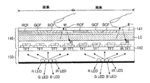
例えば、特許文献1に記載されている液晶表示装置を、図11に示す。図11は、液晶パネル140と、赤外線光源を含むバックライトユニット150とを備えている。液晶パネル140は、同一層に形成されるカラーフィルタRCF、GCF、BCFと透明窓Wとを含む上部透明基板141;画素を選択するための薄膜トランジスタ(Thin Film Transistor:以下、「TFT」という)と赤外線を感知するための赤外線感知用薄膜トランジスタ(以下、「IRTFT」という)とを含む下部透明基板142;および上部透明基板141と下部透明基板142との間に形成された液晶層LCを備えている。
この液晶パネル140の下部透明基板142上には複数のデータラインと複数のゲートラインとが直交し、また、ゲートラインと平行する複数の駆動電圧ライン、ゲートラインと駆動電圧ラインが直交する複数のリードアウトラインが形成される。また、下部透明基板142上にはデータラインとゲートラインの交差部に画素を選択するためのTFTが形成されて、駆動電圧供給ラインとリードアウトラインの交差部にIRTFTが形成されて、TFTに接続された画素電極が形成される。画素を選択するためのTFTは、ゲートラインからのスキャン信号に応じてデータラインからのデータ電圧を画素電極に供給する。IRTFTは、使用者の手あるいは不透明物質によって上部透明基板141がタッチされる際、そのタッチした点で上部透明基板141と透明窓Wとを経由して反射される赤外線の光量を感知し、その赤外線光量感知信号をリードアウトラインを通じて出力する。
この液晶パネル140に電源が供給されて、上部透明基板141上に一つ以上の指あるいは物質が接触されると、その接触面から赤外線光が反射されてIRTFTに受光される。IRTFTによって受光された赤外線光はデジタル信号処理回路でデジタル信号処理、パターン分析等をするようになる。その結果、タッチした点の座標値が計算されて、前記デジタル信号処理回路で複数のタッチした点に対して認識される。これと同時に、タッチした点のタッチイメージは液晶パネルに示される。
一方、特許文献2に記載のタッチパネルは、図12に示すように、透明絶縁基材201の上面に透明な導電膜からなる電極および平行な一対のバスバーを形成した下部電極部材204と、可撓性透明絶縁基材205の下面に透明な導電膜からなる電極206および平行な一対のバスバー207を形成した上部電極部材208とを、上下の電極間にドット状のスペーサ209を介在させ、下部電極部材204のバスバー間方向と上部電極部材208のバスバー207間方向が直交するように重ね合わせ、周縁部を接着層210で接着したアナログ抵抗膜方式の透明タッチパネルである。下部電極部材204は、左側エリアに設けられた電極パターン202Lおよび一対のバスバー203Lと、右側エリアに設けられた電極パターン202Rおよび一対のバスバー203Rとを備え、各々の分割パターンが取り出し線220を介して独立して制御される。これにより、下部電極部材204の左側エリアに設けられた電極パターン202Lと上部電極部材208に設けられた電極パターン206とが重複する左側入力エリア、下部電極部材204の右側エリアに設けられた電極パターン202Rと上部電極部材208に設けられた電極パターン206とが重複する右側入力エリア、の2つの分割入力エリアで各々ポイントを入力することができるため、左右で2ポイント同時に入力することが可能になる。
他にも特許文献3のようなマルチタッチ操作可能なパネルがある。
しかしながら、特許文献1~3に記載の構成は何れも、複数のペンで同時に文字を入力したり線を引いたりなど、複数のペンで同時に連続した入力を行う場合に、それぞれを正確に検出することができないことがある。
例えば、図13の(a)に示すように第1のペン300Aで点Aから点Bに線を引き、同時に、第2のペン300Bで点Cから点Dに線を引こうとした場合、特許文献1~3の構成では、図13の(b)に示すように、点Aから点Dに線を引き、点Cから点Bに線を引いたと間違って認識される場合がある。
これは、特許文献1~3に記載の構成の場合、複数の認識点を同時に算出しているものの、文字や線を描くためには、或る瞬間の認識点が次の時点にどの点に移動したかが分かっている必要がある。複数のペンを同時に使用するときには、ある瞬間の認識点と次の時点の認識点の近いほうを同一のペンで認識した位置として文字なり線なりを描くことは可能であるが、ペンに近寄った場合には、その判別ができなくなり、結果として、図13の(b)に示すような問題が発生する。
本発明は、上記の問題点に鑑みなされたものであり、その目的は、複数のペンを同時に使用して文字や線を描くことが可能な入力システムを提供することである。
すなわち、本発明に係る入力システムは、上記の課題を解決するために、
複数の指示具と、当該指示具による入力をセンシングして入力位置を認識するように構成された入力装置とを備えた入力システムであって、
各上記指示具の間で上記入力のタイミングを互いに異ならせて、各指示具の入力のタイミングに合わせて入力装置がセンシングする構成となっており、
上記入力装置は、指示具毎に、入力位置を時間経過に沿って順に結んで連続した入力がなされたことを検出する構成となっていることを検出する構成となっていることを特徴としている。
複数の指示具と、当該指示具による入力をセンシングして入力位置を認識するように構成された入力装置とを備えた入力システムであって、
各上記指示具の間で上記入力のタイミングを互いに異ならせて、各指示具の入力のタイミングに合わせて入力装置がセンシングする構成となっており、
上記入力装置は、指示具毎に、入力位置を時間経過に沿って順に結んで連続した入力がなされたことを検出する構成となっていることを検出する構成となっていることを特徴としている。
上記の構成によれば、センシングされるタイミングを各上記指示具の間で互いに異ならせて、当該タイミングに合わせて複数の指示具の入力を順に繰り返しセンシングするので、或る指示具による入力をセンシングする時点では、他の指示具による入力はセンシングされない。すなわち、センシングされるのは1つの指示具だけであるため、ノイズ(他の指示具による入力)を除外することができる。
そして、上記の構成によれば、タイミングを計って同じ指示具からの入力をセンシングすることができる、すなわち、一定周期で同一の指示具からの入力をセンシングすることができるので、それらの入力位置を時間経過に沿って結んでいくことによって、文字や線の入力を正確におこなうことが可能である。
このように或る時点で検出されるのは入力システム上の一点のみであるから、他の指示具からの入力に妨げられることない。よって、複数の指示具(例えば入力用のペン)を用いて同時期に連続した入力を行う場合であっても、それぞれの指示具からの入力を正確にセンシングすることができる。
本発明の他の目的、特徴、および優れた点は、以下に示す記載によって十分分かるであろう。また、本発明の利点は、添付図面を参照した次の説明で明白になるであろう。
本発明に係る入力システムは、以上のように、
複数の指示具と、当該指示具による入力をセンシングして入力位置を認識するように構成された入力装置とを備えた入力システムであって、
各上記指示具の間で上記入力のタイミングを互いに異ならせて、各指示具の入力のタイミングに合わせて入力装置がセンシングする構成となっており、
上記入力装置は、指示具毎に、入力位置を時間経過に沿って順に結んで連続した入力がなされたことを検出する構成となっていることを特徴としている。
複数の指示具と、当該指示具による入力をセンシングして入力位置を認識するように構成された入力装置とを備えた入力システムであって、
各上記指示具の間で上記入力のタイミングを互いに異ならせて、各指示具の入力のタイミングに合わせて入力装置がセンシングする構成となっており、
上記入力装置は、指示具毎に、入力位置を時間経過に沿って順に結んで連続した入力がなされたことを検出する構成となっていることを特徴としている。
これにより、ペンなどの複数の指示具を用いて同時期に文字を入力したり、線を引いたりなどの連続した入力を行う場合に、これを正確に検出することを可能にする。
〔実施形態1〕
本発明に係る入力システムの一実施形態について、図1から図5を参照して以下に説明する。
本発明に係る入力システムの一実施形態について、図1から図5を参照して以下に説明する。
(入力システムの構成)
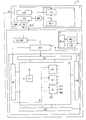
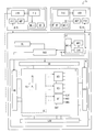
図1は、本実施形態の入力システムの構成を示すブロック図である。
図1は、本実施形態の入力システムの構成を示すブロック図である。
本発明に係る入力システムは、タッチセンサ機能、(特に文字入力機能)を備えた入力システムとして、例えば、タッチセンサ一体型入力装置として適用することができる。また、タッチセンサ機能(特に文字入力機能)を備えたあらゆる電子機器にも好適である。
本実施形態の入力システム1aは、図1に示すように、光ペン2(指示具)と、バックライトBLを有する入力装置3とを備えている。
● 光ペン(指示具)
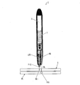
光ペン2は、発光ダイオードLEDと、圧力素子PIEと、制御基板5と、アンプ回路AMPとを備えている。
光ペン2は、発光ダイオードLEDと、圧力素子PIEと、制御基板5と、アンプ回路AMPとを備えている。
光ペン2の構成について、更に図2を用いて詳述する。
光ペン2には、図2に示すように、ペン中央部にバッテリ7が設けられ、バッテリ7のペン元側に制御基板5が設けられ、バッテリ7のペン先側に発光ダイオードLEDが配され、ペン先に圧力素子PIEが配されている。
バッテリ7は、特に制限されるものではなく、従来周知の小型のバッテリを用いることができる。
発光ダイオードLED(発光素子)は、入力装置3に設けられた光センサタッチパネル6の光センサ回路SEiによって検知される光を出射する。発光ダイオードLEDの発光は、後述する制御基板5、および入力装置3に設けられた認識エンジン10において制御される。
圧力素子PIEは、光ペン2の先端部が、入力装置3に設けられた光センサタッチパネル6の表面に押し付けられたことによって両者間に働く圧力を検知する。圧力素子PIEによる検知結果は、アンプ回路AMPを介して制御基板5のマイコンMC-1(圧力信号生成部)に入力され、例えば1024階調程度にデジタル化され、圧力信号が生成される。圧力信号は、Bluetooth(登録商標)通信回路BT-1、および入力装置3の認識エンジン10のBluetooth(登録商標)通信回路BT-2を介して認識エンジン10に入力されるようになっている。
制御基板5は、タイミングIC(TIC)と、マイコンMC-1と、Bluetooth(登録商標)通信回路BT-1とを含む。
タイミングIC(TIC)は、圧力素子PIEの検知結果、およびマイコンMC-1からの制御信号に基づいて、発光ダイオードLEDの発光を制御する。タイミングICに基づいた駆動方法については後述する。
マイコンMC-1は、Bluetooth(登録商標)通信回路BT-1、および入力装置3の認識エンジン10のBluetooth(登録商標)通信回路BT-2を介して認識エンジン10から送られる制御信号を、圧力信号とともに、タイミングIC(TIC)に送出し、発光ダイオードLEDの発光のタイミングを制御する。
Bluetooth(登録商標)通信回路BT-1は、入力装置3に設けられたBluetooth(登録商標)通信回路BT-2と無線通信をおこなう。
なお、認識エンジン10に設けられたBluetooth(登録商標)通信回路BT-2と、光ペン2の制御基板5に設けられたBluetooth(登録商標)通信回路BT-1とは、共に、Bluetooth(登録商標)に限定されるものではなく、ジグビーなどの周知の無線通信機器を採用することができる。
● 入力装置
入力装置3は、光センサタッチパネル6と、表示制御回路DCSと、バックライトBLと、認識エンジン10(制御部、出力部)とを備えている。
入力装置3は、光センサタッチパネル6と、表示制御回路DCSと、バックライトBLと、認識エンジン10(制御部、出力部)とを備えている。
光センサタッチパネル6は、表示部8と、ソースドライバSDと、ゲートドライバGDと、光センサ駆動回路LSD(出力部)と、光センサ出力回路LOD(出力部)とを含む。
表示部8には、マトリクス状に配された複数の画素Pjと、複数の走査信号線Gjと、複数のデータ信号線SLと、マトリクス状に配された複数の光センサ回路SEiと、複数のクロック信号線CLKiと、複数のリセット信号線RSTiと、複数の読み出し信号線RWSiと、複数の光センサ出力線OUT(出力部)とが設けられている(ただし、i=1・・・n、j=1・・・m)。光センサ回路SEiの構成については後述する。
表示制御回路DCSは、ソースドライバSD、ゲートドライバGD、光センサ駆動回路LSD、認識エンジン10、およびバックライトBLを制御する。
ソースドライバSDはデータ信号線SLを駆動し、ゲートドライバGDは走査信号線Gjを駆動する。
光センサ駆動回路LSDは、クロック信号線CLKi、リセット信号線RSTi、および読み出し信号線RWSiを駆動する。認識エンジン10は、光センサ出力線OUTに接続された光センサ出力回路LODを駆動する。
認識エンジン10は、マイコンMC-2と、ロジック部LGCと、メモリMRYと、Bluetooth(登録商標)通信回路BT-2とから構成されている。マイコンMC-2およびロジック部LGCにより、複数の光センサ出力線OUTから光センサ出力回路LODを介して認識エンジン10に送られたセンサ画像に基づいて、タッチ点(入力位置座標)が算出される。メモリMRYには、キャリブレーション画像がメモリされており、上記センサ画像を認識する前処理(補正)用に主に使用される。認識エンジン10に設けられたBluetooth(登録商標)通信回路BT-2は、上述した光ペン2の制御基板5に設けられたBluetooth(登録商標)通信回路BT-1と無線通信する。
(入力システムの動作(センシング))
以上のような構成を具備した入力システム1aにおいて、光ペン2の発光ダイオードLEDからの光をセンシングして入力位置、すなわち発光ダイオードLEDの照射位置を検出する。
以上のような構成を具備した入力システム1aにおいて、光ペン2の発光ダイオードLEDからの光をセンシングして入力位置、すなわち発光ダイオードLEDの照射位置を検出する。
本発明は、センシングされるタイミングを各光ペンの間で互いに異ならせて、当該タイミングに合わせて複数の各光ペンの入力を順に繰り返しセンシングすることによって、複数の光ペン2を同時に使用してもそれぞれの光ペンからの入力を正確にセンシングして、文字を入力したり線を描いたりすることができることが特徴である。
以下では、2本の光ペン2を用いた場合のセンシングについて説明するが、本発明は1本もしくは3本以上の光ペンを使用することも可能である。
本実施形態では、入力装置3が、光センサ回路SEiの感知結果を光センサ出力線OUTおよび光センサ出力回路LODを介してセンシングするタイミングをあらわす制御信号を表示制御回路DCSが生成する。この制御信号は、光ペン2の発光のタイミングを制御するとともに、センシングのタイミングを制御する信号である。
光ペン2の発光を制御するために、制御信号は、認識エンジン10に設けられたBluetooth(登録商標)通信回路BT-2から、光ペン2の制御基板5に設けられたBluetooth(登録商標)通信回路BT-1に送信され、Bluetooth(登録商標)通信回路BT-1から制御基板5に設けられたマイコンMC-1に送出される。
制御基板5のマイコンMC-1に送出された制御信号は、各光ペン2によって用いられ方が異なる。そこで、以下では、2本の光ペン2を、第1の光ペン2と、第2の光ペン2とに区別して説明する。
第1の光ペン2のマイコンMC-1では、制御信号がonとなるタイミングのうちの奇数番目のみに同期する同期信号を生成し、当該同期信号をタイミングIC(TIC)に送出する。
また、マイコンMC-1は、圧力素子PIEによって圧力が検知されると当該検知結果に基いて圧力信号を生成し、同期信号とともに圧力信号もタイミングIC(TIC)に送出する。
同期信号および圧力信号を受けたタイミングIC(TIC)は、圧力素子PIEが入力装置3に対して圧力を加えていることをあらわすデジタル信号を受け取っている場合、すなわち圧力信号がonである場合に、第1の光ペン2の先端部に配された発光ダイオードLEDを駆動して発光させる。このとき光センサタッチパネル6では、センシング動作がおこなわれる。
一方、第2の光ペン2のマイコンMC-1では、制御信号の偶数番目のみに同期する同期信号をタイミングIC(TIC)に送出する。第2の光ペン2の先端部に配された発光ダイオードLEDを駆動して発光させる方法は、第1の光ペン2と同じである。
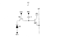
次に、発光によって、光センサ回路SEiがどのように動作するかを、図3を用いて説明する。
図3は、図1の光センサタッチパネル6に設けられる光センサ回路SEiの構成を示す回路図である。図3に示されるように、光センサ回路SEiは、フォトダイオードSPDと、トランジスタTRAと、容量Cと、トランジスタTRBとを備える。ここで、フォトダイオードSPDのアノードはリセット信号線RSTiに接続される。また、フォトダイオードSPDのカソードは、トランジスタTRAを介して、容量Cの一方の電極とトランジスタTRBの制御電極とに接続され、容量Cの他方の電極は読み出し信号線RWSiに接続される。トランジスタTRAの制御電極はクロック信号線CLKiに接続され、トランジスタTRBの一方の導通電極がVDDに接続され、他方の導通電極が光センサ出力線OUTに接続されている。光センサ出力線OUTは、光センサ出力回路LODに接続されている。
図4は、上述した駆動方法について示したタイミングチャートである。図4は、センシングと、第1の光ペン2および第2の光ペン2との間でどのように同期を取るかを具体的に示しているので、図4を用いて再び説明する。
制御信号がonのときに各光センサ回路は容量Cに光量に応じた電荷を蓄えており、制御信号がoffになった瞬間に蓄積された電荷量に応じた電位を出力する。
第1の光ペン2の同期信号は、制御信号の奇数番目のみに同期してonになる。また、第1の光ペン2に内蔵された圧力素子PIEがペン先が画面にタッチしたときの圧力を検知し、圧力信号がonとなる。第1の光ペン2は、この同期信号と圧力信号がともにonのときのみ光るように設定されている。図4では、制御信号の1,3,5のタイミングでのみ発光して、このタイミングで第1の光ペン2の座標が出力されることになる。換言すれば、制御信号の偶数番目に第1の光ペン2の圧力信号がonであっても、第1の光ペン2は発光しないし、センシングもおこなわれない。
制御信号のonとoffとの切り替わりは、1フレーム期間(1/60秒)内に1回行われる。ただし、光センサの感度が高く、高速でセンシング可能な場合は、1フレーム期間内に制御信号onとoffを2回行うことができ、2つのペンの位置座標が1フレーム期間内に取得できることになり、よりなめらかな表示を行うことができる。
次に、第2の光ペン2の同期信号は、制御信号の偶数番目のみに同期してonになる。また、上記と同様に第2の光ペン2がタッチしたときに第2の光ペン2の圧力信号がonするようになっており、図の例では、制御信号の4,6,8のタイミングで第2の光ペン2の座標が出力されることになる。換言すれば、制御信号の奇数番目に第2の光ペン2の圧力信号がonであっても、第2の光ペン2は発光しないし、センシングもおこなわれない。
このように、各センシングのタイミングではどれか1つの座標しか出力しないのでシングルタッチの方式のタッチパネルで2つのペンの座標が出力できる。
なお、光ペンが3本以上になった場合でも、制御信号がonになる各回にそれぞれ1つの光ペンの同期信号がonになるようにすれば同様にペンを特定しつつ、座標出力を実現することができる。
リセット動作は制御信号がoffからonになった瞬間に行われる。onの間に電荷蓄積を行い、onからoffになった瞬間に出力動作が行われる。
(変形例1)
本実施形態の変形例として、光ペンの圧力信号を使わない方法も考えられる。
本実施形態の変形例として、光ペンの圧力信号を使わない方法も考えられる。
この場合は、光ペンの制御信号のonのタイミングで光ペン2は必ず発光する。このとき光ペンの発光光量は、ペン先が入力装置に非常に近づいたときに光センサ回路Seiによってセンシングされ得るレベルに調整されていればよい。
(変形例2)
本実施形態では、入力装置への入力方法として発光を用いているが、本発明はこれに限定されるものではない。ペンなどの指示具からある種の信号(光センサの場合の光に相当)が発せられ、それを入力装置において受信することにより座標位置を求めるタイプの機構を採用する装置であれば、ある種の信号は光でなくてもよく、例えば、後述するような電磁誘導方式によるものであってもよく、赤外線カメラ方式によるものなどを採用することができる。
本実施形態では、入力装置への入力方法として発光を用いているが、本発明はこれに限定されるものではない。ペンなどの指示具からある種の信号(光センサの場合の光に相当)が発せられ、それを入力装置において受信することにより座標位置を求めるタイプの機構を採用する装置であれば、ある種の信号は光でなくてもよく、例えば、後述するような電磁誘導方式によるものであってもよく、赤外線カメラ方式によるものなどを採用することができる。
(入力システムを具備した電子機器の構成)
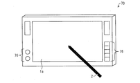
本実施形態の入力システムは、上述したように電子機器に搭載することができる。その一実施形態としてのディスプレイ機器を図5に示す。
本実施形態の入力システムは、上述したように電子機器に搭載することができる。その一実施形態としてのディスプレイ機器を図5に示す。
図5は、タッチセンサ(タッチパネル)型のディスプレイ機器を示す図である。本実施形態のディスプレイ機器70は、図5に示すように、入力システム1aが設けられている。
入力システム1aの近傍には、操作ボタン群76が設けられている。操作ボタン群76には、ディスプレイ機器70の各種設定や機能切替を行うための機能ボタン群などから構成されている。
また、本実施形態のディスプレイ機器70は、表示部に上述したタッチセンサ機能を有した入力システム1aを搭載している。したがって、例えば、上述した操作ボタン群76の一部を、ボタン操作ではなく、表示部内のタッチセンサによって操作することができる。
ディスプレイ機器70には、他にも、スピーカー、マイク、および撮像素子などが搭載されていてもよい。
(電子機器の別例)
電子機器の別例としては、電子黒板を挙げることができる。電子黒板とは、描いた内容を電子的に変換することが可能なホワイトボードであり、コピーボートと称されることもある。
電子機器の別例としては、電子黒板を挙げることができる。電子黒板とは、描いた内容を電子的に変換することが可能なホワイトボードであり、コピーボートと称されることもある。
電子黒板は、オフィスや学校などで多用されつつあるが、本発明に係る入力システムを用いれば、これらの場において、複数人が同時期に入力操作を実行していても、正確にセンシングすることができるので有意である。
また、電子黒板に限らず、大型画面の入力システムとしても適用することが可能である。
(本実施形態の作用効果)
本実施形態の構成によれば、センシングされるタイミングを各光ペンの間で互いに異ならせて、当該タイミングに合わせて複数の光ペンの入力を順に繰り返しセンシングするので、或る光ペンによる入力を検知する時点では、他の光ペンによる入力は検知されないので、或る光ペンによる入力だけがセンシングされ、ノイズ(他の光ペンによる入力)を除外することができる。
本実施形態の構成によれば、センシングされるタイミングを各光ペンの間で互いに異ならせて、当該タイミングに合わせて複数の光ペンの入力を順に繰り返しセンシングするので、或る光ペンによる入力を検知する時点では、他の光ペンによる入力は検知されないので、或る光ペンによる入力だけがセンシングされ、ノイズ(他の光ペンによる入力)を除外することができる。
そして、上記の構成によれば、タイミングを計って同じ光ペンからの入力をセンシングすることができるので、それらの入力位置を時間経過に沿って結んでいくことによって、文字や線の入力を正確におこなうことが可能である。
このように或る時点で検出されるのは入力システム上の一点のみであるから、他の光ペンからの入力に妨げられることない。よって、複数の光ペンを用いて同時期に連続した入力を行う場合であっても、それぞれの光ペンからの入力を正確にセンシングすることができる。
また、制御信号および圧力信号に基づいてセンシングのタイミングをとるので、光ペンを常時発光させる必要がなく、センシングされる時だけ発光させることができる。そのため、光ペンをセンシングされる状態で常時保持する場合と比較して、入力に関係する消費電力を低減させることができる。
また、圧力信号を生成する構成とすることによって、入力装置への入力の意志がある場合に限って、(圧力信号とともに制御信号を受けて)光ペンが入力動作をおこなえばよい。すなわち、入力装置への入力の意志がないのに、入力動作が起こることを防ぐことができる。具体例を挙げると、本構成を採用すれば、光ペンが入力装置に押し付けられていないときには、つまり入力の意志が無いときには、発光しない。これにより、無駄な発光による消費電力を省くことができる。また、他の光ペンが入力を検知されている際に、その近傍で光を発することによって誤入力を引き起こすことを回避することができる。
〔実施形態2〕
本発明に係る他の実施形態について、図6に基づいて説明すれば以下の通りである。尚、本実施形態では、上記実施形態1との相違点について説明するため、説明の便宜上、実施形態1で説明した部材と同一の機能を有する部材には同一の部材番号を付し、その説明を省略する。
本発明に係る他の実施形態について、図6に基づいて説明すれば以下の通りである。尚、本実施形態では、上記実施形態1との相違点について説明するため、説明の便宜上、実施形態1で説明した部材と同一の機能を有する部材には同一の部材番号を付し、その説明を省略する。
上述した実施形態1の入力システム1aでは、図1に示したように、認識エンジン10から送られる制御信号を無線通信機器を介してタイミングIC(TIC)に送出し、発光ダイオードLEDの発光のタイミングを制御している。これに対して、本実施形態の場合は、入力装置3のバックライトBLが赤外光生成部IRGを含む構成となっており、赤外光を所望のタイミングにあわせて発光させて、当該赤外光を光ペンにおいて受光させることで光ペンの発光タイミングを制御する構成としている。
具体的には、図6に示すように、本実施形態の入力システム1bの入力装置3´は、バックライトBLが赤外光生成部IRGを含んでいる。その代わりに、入力装置3´の認識エンジン10には、実施形態1で構成されていたBluetooth(登録商標)通信回路BT-2は無く、また、制御信号を光ペンに送出する機構も無い。
入力装置3´の表示制御回路DCSは、ソースドライバSD、ゲートドライバGD、光センサ駆動回路LSD、認識エンジン10、および、赤外光生成部IRGを含むバックライトBLを制御する。
また、本実施形態の入力システム1bの光ペン2´にはフォトダイオードPDが配されている。また、光ペン2´の制御基板5には実施形態1で構成されていたBluetooth(登録商標)通信回路BT-1は無い。
フォトダイオードPDは、入力装置3´に設けられたバックライトBL内の赤外光生成部IRGから出射された赤外光IRLを受光する。このように、光ペン2´では、入力装置3に設けられたバックライトBL内の赤外光生成部IRGからの赤外光をフォトダイオードPDにて受光(検知)できる。フォトダイオードPDによる検知結果は、アンプ回路AMPを介してタイミングIC(TIC)に入力される。
そして、光ペン2´の制御基板5に設けられているマイコンMC-1は、フォトダイオードPDおよび圧力素子PIEの検知結果に基づいて、発光ダイオードLEDの発光を制御する。
すなわち、マイコンMC-1は、タイミングIC(TIC)を介して送られるフォトダイオードPDの検知結果を受けて、発光ダイオードLEDの発光のタイミングとセンシングのタイミングとを同期するための同期信号をタイミングIC(TIC)に送出する。
以下、実施形態1と同じく第1の光ペン2´と第2の光ペン2´とを用いて説明する。
第1の光ペン2´のマイコンMC-1では、フォトダイオードPDの受光信号がonとなるタイミングのうちの奇数番目のみに同期する同期信号を生成し、当該同期信号をタイミングIC(TIC)に送出する。第1の光ペン2´のマイコンMC-1は、圧力素子PIEによって圧力が検知されると当該検知結果に基いて圧力信号を生成し、同期信号とともに圧力信号もタイミングIC(TIC)に送出する。
同期信号および圧力信号を受けたタイミングIC(TIC)は、圧力素子PIEが入力装置3に対して圧力を加えていることをあらわすデジタル信号を受け取っている場合に、第1の光ペン2の先端部に配された発光ダイオードLEDを駆動して発光させる。
一方、第2の光ペン2´のマイコンMC-1では、フォトダイオードPDの受光信号の偶数番目のみに同期する同期信号を生成し、当該同期信号をタイミングIC(TIC)に送出する。第2の光ペン2´の先端部に配された発光ダイオードLEDを駆動して発光させる方法は、第1の光ペン2と同じである。
本実施形態のように入力装置3´から赤外光を出射することによっても、上述した実施形態1と同様に、光ペン2´の発光と、当該発光に基づいた入力のセンシングとを同期させることができ、センシングのタイミングを、光ペン2´毎に互いに異ならせることによって、各光ペン2´の何れからの入力も正確にセンシングすることが可能である。
(変形例)
本実施形態では入力装置3´から赤外光を出射して光ペン2´が当該赤外光を受光する構成について説明したが、本発明はこれに限定されるものではなく、磁界の変化を用いることも可能である。すなわち、入力装置3´にコイルを設けてそこで磁界を作り、その変化を光ペン2´に設けたコイルで感知する構成とすることも可能である。これにより、磁界の変化を感知したときのみ光ペン2´が発光する構成を実現することができる。
本実施形態では入力装置3´から赤外光を出射して光ペン2´が当該赤外光を受光する構成について説明したが、本発明はこれに限定されるものではなく、磁界の変化を用いることも可能である。すなわち、入力装置3´にコイルを設けてそこで磁界を作り、その変化を光ペン2´に設けたコイルで感知する構成とすることも可能である。これにより、磁界の変化を感知したときのみ光ペン2´が発光する構成を実現することができる。
〔実施形態3〕
本発明に係る他の実施形態について、図7および図8に基づいて説明すれば以下の通りである。尚、本実施形態では、上記実施形態1との相違点について説明するため、説明の便宜上、実施形態1で説明した部材と同一の機能を有する部材には同一の部材番号を付し、その説明を省略する。
本発明に係る他の実施形態について、図7および図8に基づいて説明すれば以下の通りである。尚、本実施形態では、上記実施形態1との相違点について説明するため、説明の便宜上、実施形態1で説明した部材と同一の機能を有する部材には同一の部材番号を付し、その説明を省略する。
上述した実施形態1の入力システム1aでは、入力装置3から制御信号が全ての光ペン2に対して送出され、受信した制御信号に基づいて所定のタイミングで各光ペン2が発光する構成となっている。これに対して本実施形態では、複数の光ペン2同士が互いに通信して同期をとる。
具体的には、図7に示すように、本実施形態の入力システム1cでは、制御信号を生成する入力装置3´は、光ペン2に対して当該制御信号を送出する構成を有していない。一方、光ペン2は、光ペン2同士が無線通信するBluetooth(登録商標)通信回路BTを有している。
図8は、本実施形態の入力システム1cの駆動方法について示したタイミングチャートである。本実施形態のように光ペン2間のみで同期をとる場合、第1の光ペン2と第2の光ペン2との同期信号は、同期をとってonとoffとが逆になるように制御されている。
また、各光ペン2の同期信号のon時間は、センシングの1周期の時間(センシングがonになった瞬間から次のonになるまでの時間)以上をとるものとする。これにより、センシングとペンの同期信号との同期をとらなくてもペンの同期信号が一度onになっている間に必ずセンシングが1回以上あることになる。
また、どちらかの光ペンの同期信号(入力制御信号)がonからoffに変わって次の光ペンの同期信号がoffからonに変わるまでの時間はセンシングの制御信号の1回のon時間よりも長い。これにより、1回のセンシングの間には1つの光ペンのみが光っている状態を実現することができる。
このように、本実施形態の構成によっても、上述した各実施形態と同様に、センシングのタイミングを、光ペン2´毎に互いに異ならせることによって、各光ペン2´の何れからの入力も正確にセンシングすることが可能である。
〔実施形態4〕
本発明に係る他の実施形態について、図9に基づいて説明すれば以下の通りである。尚、本実施形態では、上記実施形態1との相違点について説明するため、説明の便宜上、実施形態1で説明した部材と同一の機能を有する部材には同一の部材番号を付し、その説明を省略する。
本発明に係る他の実施形態について、図9に基づいて説明すれば以下の通りである。尚、本実施形態では、上記実施形態1との相違点について説明するため、説明の便宜上、実施形態1で説明した部材と同一の機能を有する部材には同一の部材番号を付し、その説明を省略する。
上述した実施形態1の入力システム1aでは、図1に示したように、光ペンを用いて光によって入力装置に入力をおこなう構成である。これに対して、本実施形態の入力システム1dは、図9に示すように、入力装置3´´に入力をおこなう手段として、電磁ペン20を用いている。電磁ペン20にはコイル22とBluetooth(登録商標)通信回路BTとが内蔵されており、このコイル22により、ペン近傍の磁界を変化させる。Bluetooth(登録商標)通信回路BTは、磁気ペン20同士の間で同期をとるために用いても良いし、入力装置3´´側にBluetooth(登録商標)通信回路を設けて、これと磁気ペン20のBluetooth(登録商標)通信回路BTとの間で通信しても良い。
一方、入力装置3´´側には、その磁界の変化を検知するためのコイル30が内蔵されており、ペンの位置を求めることができる。
このとき、各電磁ペン20からの磁界を、上述した実施形態1~3と同様の手法で制御することにより、入力装置3´´側で得られた座標が、どちらの電磁ペンのものであるか判る。
センシングのタイミングと磁界変化のタイミングとを同期させる手法は、上述した実施形態1のように入力装置から指示具(光ペン)に送出される制御信号を用いるものであってもよく、実施形態3のように、指示具同士が互いに同期をとってもよい。
〔実施形態5〕
本発明に係る他の実施形態について、図10に基づいて説明すれば以下の通りである。尚、本実施形態では、上記実施形態1との相違点について説明するため、説明の便宜上、実施形態1で説明した部材と同一の機能を有する部材には同一の部材番号を付し、その説明を省略する。
本発明に係る他の実施形態について、図10に基づいて説明すれば以下の通りである。尚、本実施形態では、上記実施形態1との相違点について説明するため、説明の便宜上、実施形態1で説明した部材と同一の機能を有する部材には同一の部材番号を付し、その説明を省略する。
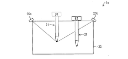
上述した実施形態1の入力システム1aでは、図1に示したように、光ペンを用いて光によって入力装置に入力をおこなう構成である。これに対して、本実施形態の入力システム1eは、図10に示すように、入力装置33に入力をおこなう手段として、赤外光を出射するペン21を用いている。ペン21には赤外光を発する赤外光源が内蔵されており、この赤外光源により、ペン先端部から赤外光を出射する。
一方、入力装置33側には、その画面に近接しているペン21から出射する赤外光を受光する複数の赤外線カメラ25aおよび25bが設けられている。赤外線カメラは画面に隣接した互いに異なる少なくとも2地点に配置されている。これにより、三角測量の原理によって1つのペンの座標位置を求めることができる。
このとき、各ペン21から発する赤外線を、上述した実施形態1~3と同様の手法で制御することにより、入力装置33側で得られた座標が、どちらのペンのものであるか判る。
なお、本発明は上述した各実施形態に限定されるものではない。当業者は、請求項に示した範囲内において、本発明をいろいろと変更できる。すなわち、請求項に示した範囲内において、適宜変更された技術的手段を組み合わせれば、新たな実施形態が得られる。すなわち、発明の詳細な説明の項においてなされた具体的な実施形態は、あくまでも、本発明の技術内容を明らかにするものであって、そのような具体例にのみ限定して狭義に解釈されるべきものではなく、本発明の精神と次に記載する請求の範囲内で、いろいろと変更して実施することができるものである。
(本発明の総括)
本発明に係る入力システムは、以上のように、
複数の指示具と、当該指示具による入力をセンシングして入力位置を認識するように構成された入力装置とを備えた入力システムであって、
各上記指示具の間で上記入力のタイミングを互いに異ならせて、各指示具の入力のタイミングに合わせて入力装置がセンシングする構成となっており、
上記入力装置は、指示具毎に、入力位置を時間経過に沿って順に結んで連続した入力がなされたことを検出する構成となっていることを検出する構成となっていることを特徴としている。
本発明に係る入力システムは、以上のように、
複数の指示具と、当該指示具による入力をセンシングして入力位置を認識するように構成された入力装置とを備えた入力システムであって、
各上記指示具の間で上記入力のタイミングを互いに異ならせて、各指示具の入力のタイミングに合わせて入力装置がセンシングする構成となっており、
上記入力装置は、指示具毎に、入力位置を時間経過に沿って順に結んで連続した入力がなされたことを検出する構成となっていることを検出する構成となっていることを特徴としている。
上記の構成によれば、センシングされるタイミングを各上記指示具の間で互いに異ならせて、当該タイミングに合わせて複数の指示具の入力を順に繰り返しセンシングするので、或る指示具による入力をセンシングする時点では、他の指示具による入力はセンシングされない。すなわち、センシングされるのは1つの指示具だけであるため、ノイズ(他の指示具による入力)を除外することができる。
そして、上記の構成によれば、タイミングを計って同じ指示具からの入力をセンシングすることができる、すなわち、一定周期で同一の指示具からの入力をセンシングすることができるので、それらの入力位置を時間経過に沿って結んでいくことによって、文字や線の入力を正確におこなうことが可能である。
このように或る時点で検出されるのは入力システム上の一点のみであるから、他の指示具からの入力に妨げられることない。よって、複数の指示具(例えば入力用のペン)を用いて同時期に連続した入力を行う場合であっても、それぞれの指示具からの入力を正確にセンシングすることができる。
また、本発明に係る入力システムの一形態としては、上記の構成に加えて、
上記入力装置は、上記指示具の入力をセンシングするタイミングを示す制御信号を生成して、当該制御信号を指示具それぞれに送出する制御部と、上記制御信号に基づいて上記指示具の入力をセンシングする出力部とを有しており、
上記指示具は、上記制御信号を受信する受信部を有しており、受信した当該制御信号に基づいて上記入力装置への入力をおこなう構成となっており、
各上記指示具は互いに異なるタイミングで、上記制御信号にあわせて上記入力装置への入力をおこなう、ことが好ましい。
上記入力装置は、上記指示具の入力をセンシングするタイミングを示す制御信号を生成して、当該制御信号を指示具それぞれに送出する制御部と、上記制御信号に基づいて上記指示具の入力をセンシングする出力部とを有しており、
上記指示具は、上記制御信号を受信する受信部を有しており、受信した当該制御信号に基づいて上記入力装置への入力をおこなう構成となっており、
各上記指示具は互いに異なるタイミングで、上記制御信号にあわせて上記入力装置への入力をおこなう、ことが好ましい。
上記の構成によれば、指示具は、制御信号に基づいて上記入力装置への入力をおこなう構成となっているので、例えば光ペンを指示具として用いた場合に、光ペンを常時発光させる必要がなく、センシングされる時だけ発光させることができる。
そのため、指示具をセンシングされる状態で常時保持する場合と比較して、入力に関係する消費電力を低減させることができる。
また、本発明に係る入力システムの一形態としては、上記の構成に加えて、
上記入力装置は、上記指示具の入力をセンシングするタイミングを示す制御信号を生成する制御部と、当該制御信号に基づいて赤外光を発する光源部と、上記制御信号に基づいて上記指示具の入力をセンシングする出力部とを有しており、
上記指示具は、上記赤外光を受光して受光信号を生成するフォトダイオードと、当該受光信号に基づいて上記入力装置への入力をおこなう構成となっており、
各上記指示具は互いに異なるタイミングで上記受光信号にあわせて上記入力装置への入力をおこなう、ことが好ましい。
上記入力装置は、上記指示具の入力をセンシングするタイミングを示す制御信号を生成する制御部と、当該制御信号に基づいて赤外光を発する光源部と、上記制御信号に基づいて上記指示具の入力をセンシングする出力部とを有しており、
上記指示具は、上記赤外光を受光して受光信号を生成するフォトダイオードと、当該受光信号に基づいて上記入力装置への入力をおこなう構成となっており、
各上記指示具は互いに異なるタイミングで上記受光信号にあわせて上記入力装置への入力をおこなう、ことが好ましい。
上記の構成によれば、指示具は、制御信号としての赤外光が指示具のフォトダイオードに感知されたときだけ記入力装置への入力をおこなう構成とすることができるので、例えば光ペンを指示具として用いた場合に、光ペンを常時発光させる必要がなく、指示具のフォトダイオードが赤外光を感知したときだけ、すなわち、センシングされるタイミングの時だけ発光させることができる。
そのため、指示具をセンシングされる状態で常時保持する場合と比較して、入力に関係する消費電力を低減させることができる。
また、本発明に係る入力システムの一形態としては、上記の構成に加えて、
上記入力装置は、上記指示具の入力をセンシングするタイミングを示す制御信号を生成する制御部と、上記制御信号に基づいて上記指示具の入力をセンシングする出力部とを有しており、
各上記指示具は互いに異なるタイミングで上記入力装置への入力をおこなうよう当該入力を制御する入力制御信号であって、上記制御信号と同調した当該入力制御信号を指示具同士の間で送受する構成となっている、ことが好ましい。
上記入力装置は、上記指示具の入力をセンシングするタイミングを示す制御信号を生成する制御部と、上記制御信号に基づいて上記指示具の入力をセンシングする出力部とを有しており、
各上記指示具は互いに異なるタイミングで上記入力装置への入力をおこなうよう当該入力を制御する入力制御信号であって、上記制御信号と同調した当該入力制御信号を指示具同士の間で送受する構成となっている、ことが好ましい。
上記の構成によれば、指示具は、制御信号に基づいて上記入力装置への入力をおこなう構成となっているので、例えば光ペンを指示具として用いた場合に、常時発光させる必要はなく、センシングされる時だけ発光させることができる。
そのため、指示具をセンシングされる状態で常時保持する場合と比較して、入力に関係する消費電力を低減させることができる。
例えば光ペンを指示具として用いた場合に、常時発光させることなく、指示具のフォトダイオードが赤外線を感知したときだけ、すなわち、センシングされるタイミングの時だけ発光させることができる。
そのため、指示具をセンシングされる状態で常時保持する場合と比較して、入力に関係する消費電力を低減させることができる。
また、本発明に係る入力システムの一形態としては、上記の構成に加えて、
上記指示具は、その先端部を上記入力装置に押し付けたときに生じる圧力を感知すると圧力信号を生成する圧力信号生成部を有しており、
上記指示具は、入力装置への入力をおこなう条件として、上記圧力信号が生成されることを必須条件とする、ことが好ましい。
上記指示具は、その先端部を上記入力装置に押し付けたときに生じる圧力を感知すると圧力信号を生成する圧力信号生成部を有しており、
上記指示具は、入力装置への入力をおこなう条件として、上記圧力信号が生成されることを必須条件とする、ことが好ましい。
上記の構成によれば、圧力信号が生成されるのは、入力装置への入力の意志があることを示しており、その場合に限って、(制御信号を受けて)指示具が入力動作をおこなえばよい。すなわち、入力装置への入力の意志がないのに、入力動作が起こることを防ぐことができる。具体例を挙げると、光ペンを指示具とする場合、本構成を採用すれば、光ペンが入力装置に押し付けられていないときには、つまり入力の意志が無いときには、発光しない。これにより、無駄な発光による消費電力を省くことができるとともに、誤入力を回避することができる。
また、本発明に係る入力システムの一形態としては、具体的には、
上記指示具が、入力装置への入力をおこなう手段として、光を出射する発光素子を有しており、
上記入力装置が、上記発光素子の光を受光して当該受光位置を上記入力位置としてセンシングする構成とすることができる。
上記指示具が、入力装置への入力をおこなう手段として、光を出射する発光素子を有しており、
上記入力装置が、上記発光素子の光を受光して当該受光位置を上記入力位置としてセンシングする構成とすることができる。
また、本発明に係る入力システムは、上記とは別の具体例として、
上記指示具が、入力装置への入力をおこなう手段として、磁界を変えるコイルを有しており、
上記入力装置が、上記コイルによる磁界の変化を検知して当該変化した位置を上記入力位置としてセンシングする構成となっていてもよい。
上記指示具が、入力装置への入力をおこなう手段として、磁界を変えるコイルを有しており、
上記入力装置が、上記コイルによる磁界の変化を検知して当該変化した位置を上記入力位置としてセンシングする構成となっていてもよい。
また、本発明に係る入力システムの一形態としては、上記とは更に別の具体例として、
上記指示具が、赤外光を発することによって上記入力装置への入力をおこなう構成となっており、
上記入力装置が、互いに異なる位置から上記指示具が発する赤外光を受光する複数の受光素子を有しており、当該複数の受光素子からの受光結果に基づいて当該赤外光が照射された位置を上記入力位置としてセンシングする構成であってもよい。
上記指示具が、赤外光を発することによって上記入力装置への入力をおこなう構成となっており、
上記入力装置が、互いに異なる位置から上記指示具が発する赤外光を受光する複数の受光素子を有しており、当該複数の受光素子からの受光結果に基づいて当該赤外光が照射された位置を上記入力位置としてセンシングする構成であってもよい。
また、本発明に係る入力システムの一形態としては、上記の構成に加えて、
上記指示具が上記制御信号を無線通信によって受信する構成となっている、ことが好ましい。
上記指示具が上記制御信号を無線通信によって受信する構成となっている、ことが好ましい。
上記の構成によれば、入力信号に上記制御信号を受信させるために有線を配線する必要がなく、指示具の操作自由度および使用感を向上させることができる。特に、本発明の場合、複数の指示具を用いることを前提としているため、無線通信であることは有意である。
また、本発明に係る入力システムの一形態としては、上記の構成に加えて、
上記指示具が上記入力制御信号を無線通信する構成となっている、ことが好ましい。
上記指示具が上記入力制御信号を無線通信する構成となっている、ことが好ましい。
上記の構成によれば、入力信号同士を有線でつなぐ必要がなく、指示具の操作自由度および使用感を向上させることができる。特に、本発明の場合、複数の指示具を用いることを前提としているため、無線通信であることは有意である。
本発明は、表示機能を有する液晶パネルにタッチパネル機能を兼ね備えた入力装置としてあらゆる電子機器の入力装置に搭載することができる。
1a~1e 入力システム
2 光ペン、第1の光ペン、第2の光ペン(指示具)
3、33 入力装置
5 制御基板
6 光センサタッチパネル
7 バッテリ
8 表示部
10 認識エンジン(制御部、出力部)
20 電磁ペン(指示具)
21 ペン(指示具)
22 電磁ペン側のコイル
25a、25b 赤外線カメラ(受光素子)
30 入力装置側のコイル
70 ディスプレイ機器
76 操作ボタン群
AMP アンプ回路
BL バックライト
BT、BT-1、BT-2 Bluetooth(登録商標)通信回路
C 容量
CLKi クロック信号線
DCS 表示制御回路
GD ゲートドライバ
Gj 走査信号線
IC タイミング
IRG 赤外光生成部
IRL 赤外光
LED 発光ダイオード(発光素子)
LGC ロジック部
LOD 光センサ出力回路
LSD 光センサ駆動回路
MC-1 マイコン(圧力信号生成部)
MC-2 マイコン
MRY メモリ
OUT 光センサ出力線
PD フォトダイオード
PIE 圧力素子
Pj 画素
RSTi リセット信号線
RWSi 読み出し信号線
SD ソースドライバ
SEi 光センサ回路
SL データ信号線
SPD フォトダイオード
Sei 光センサ回路
TRA トランジスタ
TRB トランジスタ
2 光ペン、第1の光ペン、第2の光ペン(指示具)
3、33 入力装置
5 制御基板
6 光センサタッチパネル
7 バッテリ
8 表示部
10 認識エンジン(制御部、出力部)
20 電磁ペン(指示具)
21 ペン(指示具)
22 電磁ペン側のコイル
25a、25b 赤外線カメラ(受光素子)
30 入力装置側のコイル
70 ディスプレイ機器
76 操作ボタン群
AMP アンプ回路
BL バックライト
BT、BT-1、BT-2 Bluetooth(登録商標)通信回路
C 容量
CLKi クロック信号線
DCS 表示制御回路
GD ゲートドライバ
Gj 走査信号線
IC タイミング
IRG 赤外光生成部
IRL 赤外光
LED 発光ダイオード(発光素子)
LGC ロジック部
LOD 光センサ出力回路
LSD 光センサ駆動回路
MC-1 マイコン(圧力信号生成部)
MC-2 マイコン
MRY メモリ
OUT 光センサ出力線
PD フォトダイオード
PIE 圧力素子
Pj 画素
RSTi リセット信号線
RWSi 読み出し信号線
SD ソースドライバ
SEi 光センサ回路
SL データ信号線
SPD フォトダイオード
Sei 光センサ回路
TRA トランジスタ
TRB トランジスタ
Claims (10)
- 複数の指示具と、当該指示具による入力をセンシングして入力位置を認識するように構成された入力装置とを備えた入力システムであって、
各上記指示具の間で上記入力のタイミングを互いに異ならせて、各指示具の入力のタイミングに合わせて入力装置がセンシングする構成となっており、
上記入力装置は、指示具毎に、入力位置を時間経過に沿って順に結んで連続した入力がなされたことを検出する構成となっていることを特徴とする入力システム。 - 上記入力装置は、上記指示具の入力をセンシングするタイミングを示す制御信号を生成して、当該制御信号を指示具それぞれに送出する制御部と、上記制御信号に基づいて上記指示具の入力をセンシングする出力部とを有しており、
上記指示具は、上記制御信号を受信する受信部を有しており、受信した当該制御信号に基づいて上記入力装置への入力をおこなう構成となっており、
各上記指示具は互いに異なるタイミングで、上記制御信号にあわせて上記入力装置への入力をおこなう、ことを特徴とする請求項1に記載の入力システム。 - 上記入力装置は、上記指示具の入力をセンシングするタイミングを示す制御信号を生成する制御部と、当該制御信号に基づいて赤外光を発する光源部と、上記制御信号に基づいて上記指示具の入力をセンシングする出力部とを有しており、
上記指示具は、上記赤外光を受光して受光信号を生成するフォトダイオードと、当該受光信号に基づいて上記入力装置への入力をおこなう構成となっており、
各上記指示具は互いに異なるタイミングで上記受光信号にあわせて上記入力装置への入力をおこなう、ことを特徴とする請求項1または2に記載の入力システム。 - 上記入力装置は、上記指示具の入力をセンシングするタイミングを示す制御信号を生成する制御部と、上記制御信号に基づいて上記指示具の入力をセンシングする出力部とを有しており、
各上記指示具は互いに異なるタイミングで上記入力装置への入力をおこなうよう当該入力を制御する入力制御信号であって、上記制御信号と同調した当該入力制御信号を指示具同士の間で送受する構成となっている、ことを特徴とする請求項1または2に記載の入力システム。 - 上記指示具は、その先端部を上記入力装置に押し付けたときに生じる圧力を感知すると圧力信号を生成する圧力信号生成部を有しており、
上記指示具は、入力装置への入力をおこなう条件として、上記圧力信号が生成されることを必須条件とする、ことを特徴とする請求項1から4までの何れか1項に記載の入力システム。 - 上記指示具は、入力装置への入力をおこなう手段として、光を出射する発光素子を有しており、
上記入力装置は、上記発光素子の光を受光して当該受光位置を上記入力位置としてセンシングする構成となっていることを特徴とする請求項1から5までの何れか1項に記載の入力システム。 - 上記指示具が、入力装置への入力をおこなう手段として、磁界を変えるコイルを有しており、
上記入力装置が、上記コイルによる磁界の変化を検知して当該変化した位置を上記入力位置としてセンシングする構成となっていることを特徴とする請求項1から5までの何れか1項に記載の入力システム。 - 上記指示具が、赤外光を発することによって上記入力装置への入力をおこなう構成となっており、
上記入力装置が、互いに異なる位置から上記指示具が発する赤外光を受光する複数の受光素子を有しており、当該複数の受光素子からの受光結果に基づいて当該赤外光が照射された位置を上記入力位置としてセンシングする構成となっていることを特徴とする請求項1から5までの何れか1項に記載の入力システム。 - 上記指示具が上記制御信号を無線通信によって受信する構成となっていることを特徴とする請求項2に記載の入力システム。
- 上記指示具が上記入力制御信号を無線通信によって受信する構成となっていることを特徴とする請求項4に記載の入力システム。
Priority Applications (1)
| Application Number | Priority Date | Filing Date | Title |
|---|---|---|---|
| US13/993,204 US20130257782A1 (en) | 2010-12-14 | 2011-12-07 | Input system |
Applications Claiming Priority (2)
| Application Number | Priority Date | Filing Date | Title |
|---|---|---|---|
| JP2010278498 | 2010-12-14 | ||
| JP2010-278498 | 2010-12-14 |
Publications (1)
| Publication Number | Publication Date |
|---|---|
| WO2012081473A1 true WO2012081473A1 (ja) | 2012-06-21 |
Family
ID=46244580
Family Applications (1)
| Application Number | Title | Priority Date | Filing Date |
|---|---|---|---|
| PCT/JP2011/078322 Ceased WO2012081473A1 (ja) | 2010-12-14 | 2011-12-07 | 入力システム |
Country Status (2)
| Country | Link |
|---|---|
| US (1) | US20130257782A1 (ja) |
| WO (1) | WO2012081473A1 (ja) |
Cited By (3)
| Publication number | Priority date | Publication date | Assignee | Title |
|---|---|---|---|---|
| WO2014091225A1 (en) * | 2012-12-12 | 2014-06-19 | Modular Software Limited T/A Reflective Thinking | Method and apparatus for tracking the movement of a plurality of tracked devices within a scene |
| JP2017072956A (ja) * | 2015-10-06 | 2017-04-13 | 大日本印刷株式会社 | 線分入力システム |
| US20230022806A1 (en) * | 2020-01-09 | 2023-01-26 | Sony Group Corporation | Information processing apparatus, information processing method, and program |
Families Citing this family (9)
| Publication number | Priority date | Publication date | Assignee | Title |
|---|---|---|---|---|
| JP5994300B2 (ja) * | 2012-03-12 | 2016-09-21 | ブラザー工業株式会社 | 入力装置及び入力プログラム |
| US20140062966A1 (en) * | 2012-09-05 | 2014-03-06 | Research In Motion Limited | Stylus Having a Flexibly-Resilient Tip |
| JP6264003B2 (ja) * | 2013-12-09 | 2018-01-24 | 株式会社リコー | 座標入力システム、座標指示部、座標入力部、座標入力システムの制御方法、及びプログラム |
| JP6279916B2 (ja) * | 2014-01-31 | 2018-02-14 | シャープ株式会社 | タッチパネル装置 |
| TWI511008B (zh) * | 2014-05-26 | 2015-12-01 | Wistron Corp | 偵測觸控方法及其光學觸控系統 |
| CN106325610B (zh) * | 2015-06-30 | 2019-06-11 | 中强光电股份有限公司 | 触控显示系统、触控装置与触控显示方法 |
| US20180239445A1 (en) * | 2017-02-20 | 2018-08-23 | Microsoft Technology Licensing, Llc | Device and method for communicating with a stylus |
| KR102694238B1 (ko) * | 2018-11-22 | 2024-08-13 | 삼성전자주식회사 | 안테나를 포함하는 디지털 펜의 구조 |
| KR20210025745A (ko) * | 2019-08-27 | 2021-03-10 | 삼성디스플레이 주식회사 | 지문 감지 화소 및 전자펜 감지 화소를 포함하는 감지 패널 및 그것을 포함하는 표시 장치 |
Citations (2)
| Publication number | Priority date | Publication date | Assignee | Title |
|---|---|---|---|---|
| JP2003256123A (ja) * | 2002-03-01 | 2003-09-10 | Ricoh Co Ltd | 座標検出装置 |
| JP2009289243A (ja) * | 2008-06-02 | 2009-12-10 | Mitsubishi Electric Corp | 位置検出装置、位置検出システム、映像表示装置、及び映像表示システム |
Family Cites Families (2)
| Publication number | Priority date | Publication date | Assignee | Title |
|---|---|---|---|---|
| JP3186946B2 (ja) * | 1994-05-31 | 2001-07-11 | シャープ株式会社 | 座標検出装置 |
| US20080169132A1 (en) * | 2007-01-03 | 2008-07-17 | Yao Ding | Multiple styli annotation system |
-
2011
- 2011-12-07 WO PCT/JP2011/078322 patent/WO2012081473A1/ja not_active Ceased
- 2011-12-07 US US13/993,204 patent/US20130257782A1/en not_active Abandoned
Patent Citations (2)
| Publication number | Priority date | Publication date | Assignee | Title |
|---|---|---|---|---|
| JP2003256123A (ja) * | 2002-03-01 | 2003-09-10 | Ricoh Co Ltd | 座標検出装置 |
| JP2009289243A (ja) * | 2008-06-02 | 2009-12-10 | Mitsubishi Electric Corp | 位置検出装置、位置検出システム、映像表示装置、及び映像表示システム |
Cited By (4)
| Publication number | Priority date | Publication date | Assignee | Title |
|---|---|---|---|---|
| WO2014091225A1 (en) * | 2012-12-12 | 2014-06-19 | Modular Software Limited T/A Reflective Thinking | Method and apparatus for tracking the movement of a plurality of tracked devices within a scene |
| JP2017072956A (ja) * | 2015-10-06 | 2017-04-13 | 大日本印刷株式会社 | 線分入力システム |
| US20230022806A1 (en) * | 2020-01-09 | 2023-01-26 | Sony Group Corporation | Information processing apparatus, information processing method, and program |
| US11836300B2 (en) * | 2020-01-09 | 2023-12-05 | Sony Group Corporation | Information processing apparatus and information processing method |
Also Published As
| Publication number | Publication date |
|---|---|
| US20130257782A1 (en) | 2013-10-03 |
Similar Documents
| Publication | Publication Date | Title |
|---|---|---|
| WO2012081473A1 (ja) | 入力システム | |
| US10955964B2 (en) | Active pen and touchscreen display device | |
| CN108153376B (zh) | 显示设备 | |
| CN105278729B (zh) | 具有集成触摸屏的显示设备 | |
| KR102043370B1 (ko) | 압력 센서부를 이용한 플렉서블 표시장치의 사용자 입력 제어 방법 | |
| TWI543034B (zh) | 具有觸控感測器之顯示裝置及其驅動方法 | |
| JP6191064B2 (ja) | 静電容量誘導式タッチ方法 | |
| TWI649688B (zh) | 觸碰控制器、觸碰感測裝置、電子裝置、顯示裝置以及觸碰感測方法 | |
| JP6249486B2 (ja) | 描画装置 | |
| KR101351418B1 (ko) | 적외선 센서 모듈을 이용한 표시 장치 및 그의 구동 방법 | |
| US20060214892A1 (en) | Display device and display method | |
| US20100207910A1 (en) | Optical Sensing Screen and Panel Sensing Method | |
| JP2007305110A (ja) | 力・位置感知ディスプレイ | |
| KR20180045944A (ko) | 터치센서를 구비하는 표시장치 및 그에 대한 터치감지방법 | |
| CN104067205B (zh) | 部分地与lcd显示器集成的电容式触摸感应器 | |
| CN102446022B (zh) | 触控屏幕系统 | |
| JP2016224808A (ja) | タッチ検出機能付き表示システム | |
| CN101727248A (zh) | 用于执行闪光模式的触摸屏显示装置和操作该装置的方法 | |
| US20130285981A1 (en) | Display module, electronic device and control method thereof | |
| CN109144302B (zh) | 触控面板及其触控方法、触控装置 | |
| US20130113758A1 (en) | Method and system for recognizing touch point, and display apparatus | |
| KR20190018951A (ko) | 센싱부를 포함하는 표시장치 및 그를 이용한 센싱방법 | |
| WO2011129159A1 (ja) | 入力表示装置、入力装置、入力装置の制御方法 | |
| KR102202871B1 (ko) | 액정표시장치 | |
| KR102320770B1 (ko) | 표시장치의 터치 인식방법 및 이를 이용한 표시장치 |
Legal Events
| Date | Code | Title | Description |
|---|---|---|---|
| 121 | Ep: the epo has been informed by wipo that ep was designated in this application |
Ref document number: 11848525 Country of ref document: EP Kind code of ref document: A1 |
|
| WWE | Wipo information: entry into national phase |
Ref document number: 13993204 Country of ref document: US |
|
| NENP | Non-entry into the national phase |
Ref country code: DE |
|
| 122 | Ep: pct application non-entry in european phase |
Ref document number: 11848525 Country of ref document: EP Kind code of ref document: A1 |
|
| NENP | Non-entry into the national phase |
Ref country code: JP |