WO2012081237A1 - Semiconductor device and method for controlling same - Google Patents
Semiconductor device and method for controlling same Download PDFInfo
- Publication number
- WO2012081237A1 WO2012081237A1 PCT/JP2011/006961 JP2011006961W WO2012081237A1 WO 2012081237 A1 WO2012081237 A1 WO 2012081237A1 JP 2011006961 W JP2011006961 W JP 2011006961W WO 2012081237 A1 WO2012081237 A1 WO 2012081237A1
- Authority
- WO
- WIPO (PCT)
- Prior art keywords
- gate electrode
- current
- ohmic
- electrode
- voltage
- Prior art date
Links
- 239000004065 semiconductor Substances 0.000 title claims abstract description 194
- 238000000034 method Methods 0.000 title claims description 16
- 239000000758 substrate Substances 0.000 claims description 32
- XUIMIQQOPSSXEZ-UHFFFAOYSA-N Silicon Chemical compound [Si] XUIMIQQOPSSXEZ-UHFFFAOYSA-N 0.000 claims description 5
- 229910052710 silicon Inorganic materials 0.000 claims description 5
- 239000010703 silicon Substances 0.000 claims description 5
- HBMJWWWQQXIZIP-UHFFFAOYSA-N silicon carbide Chemical compound [Si+]#[C-] HBMJWWWQQXIZIP-UHFFFAOYSA-N 0.000 claims description 5
- 229910052594 sapphire Inorganic materials 0.000 claims description 4
- 239000010980 sapphire Substances 0.000 claims description 4
- 229910010271 silicon carbide Inorganic materials 0.000 claims description 3
- 230000004048 modification Effects 0.000 description 14
- 238000012986 modification Methods 0.000 description 14
- 230000007423 decrease Effects 0.000 description 12
- 238000010586 diagram Methods 0.000 description 9
- 229910002601 GaN Inorganic materials 0.000 description 7
- JMASRVWKEDWRBT-UHFFFAOYSA-N Gallium nitride Chemical compound [Ga]#N JMASRVWKEDWRBT-UHFFFAOYSA-N 0.000 description 5
- PXHVJJICTQNCMI-UHFFFAOYSA-N Nickel Chemical compound [Ni] PXHVJJICTQNCMI-UHFFFAOYSA-N 0.000 description 5
- 239000000470 constituent Substances 0.000 description 4
- 239000000463 material Substances 0.000 description 3
- 230000015556 catabolic process Effects 0.000 description 2
- 230000000694 effects Effects 0.000 description 2
- 229910052759 nickel Inorganic materials 0.000 description 2
- 230000010287 polarization Effects 0.000 description 2
- 239000010936 titanium Substances 0.000 description 2
- 230000001052 transient effect Effects 0.000 description 2
- 229910052581 Si3N4 Inorganic materials 0.000 description 1
- 229910004298 SiO 2 Inorganic materials 0.000 description 1
- VYPSYNLAJGMNEJ-UHFFFAOYSA-N Silicium dioxide Chemical compound O=[Si]=O VYPSYNLAJGMNEJ-UHFFFAOYSA-N 0.000 description 1
- RTAQQCXQSZGOHL-UHFFFAOYSA-N Titanium Chemical compound [Ti] RTAQQCXQSZGOHL-UHFFFAOYSA-N 0.000 description 1
- 229910052782 aluminium Inorganic materials 0.000 description 1
- XAGFODPZIPBFFR-UHFFFAOYSA-N aluminium Chemical compound [Al] XAGFODPZIPBFFR-UHFFFAOYSA-N 0.000 description 1
- RNQKDQAVIXDKAG-UHFFFAOYSA-N aluminum gallium Chemical compound [Al].[Ga] RNQKDQAVIXDKAG-UHFFFAOYSA-N 0.000 description 1
- 230000002457 bidirectional effect Effects 0.000 description 1
- 230000003247 decreasing effect Effects 0.000 description 1
- 230000005684 electric field Effects 0.000 description 1
- 230000005669 field effect Effects 0.000 description 1
- 238000004519 manufacturing process Methods 0.000 description 1
- 150000004767 nitrides Chemical class 0.000 description 1
- 229920006395 saturated elastomer Polymers 0.000 description 1
- HQVNEWCFYHHQES-UHFFFAOYSA-N silicon nitride Chemical compound N12[Si]34N5[Si]62N3[Si]51N64 HQVNEWCFYHHQES-UHFFFAOYSA-N 0.000 description 1
- 229910052814 silicon oxide Inorganic materials 0.000 description 1
- 230000002269 spontaneous effect Effects 0.000 description 1
- 229910052719 titanium Inorganic materials 0.000 description 1
- 230000009466 transformation Effects 0.000 description 1
- 230000005533 two-dimensional electron gas Effects 0.000 description 1
Images


Classifications
-
- H—ELECTRICITY
- H01—ELECTRIC ELEMENTS
- H01L—SEMICONDUCTOR DEVICES NOT COVERED BY CLASS H10
- H01L29/00—Semiconductor devices adapted for rectifying, amplifying, oscillating or switching, or capacitors or resistors with at least one potential-jump barrier or surface barrier, e.g. PN junction depletion layer or carrier concentration layer; Details of semiconductor bodies or of electrodes thereof ; Multistep manufacturing processes therefor
- H01L29/66—Types of semiconductor device ; Multistep manufacturing processes therefor
- H01L29/68—Types of semiconductor device ; Multistep manufacturing processes therefor controllable by only the electric current supplied, or only the electric potential applied, to an electrode which does not carry the current to be rectified, amplified or switched
- H01L29/76—Unipolar devices, e.g. field effect transistors
- H01L29/772—Field effect transistors
- H01L29/778—Field effect transistors with two-dimensional charge carrier gas channel, e.g. HEMT ; with two-dimensional charge-carrier layer formed at a heterojunction interface
- H01L29/7786—Field effect transistors with two-dimensional charge carrier gas channel, e.g. HEMT ; with two-dimensional charge-carrier layer formed at a heterojunction interface with direct single heterostructure, i.e. with wide bandgap layer formed on top of active layer, e.g. direct single heterostructure MIS-like HEMT
-
- H—ELECTRICITY
- H01—ELECTRIC ELEMENTS
- H01L—SEMICONDUCTOR DEVICES NOT COVERED BY CLASS H10
- H01L29/00—Semiconductor devices adapted for rectifying, amplifying, oscillating or switching, or capacitors or resistors with at least one potential-jump barrier or surface barrier, e.g. PN junction depletion layer or carrier concentration layer; Details of semiconductor bodies or of electrodes thereof ; Multistep manufacturing processes therefor
- H01L29/02—Semiconductor bodies ; Multistep manufacturing processes therefor
- H01L29/06—Semiconductor bodies ; Multistep manufacturing processes therefor characterised by their shape; characterised by the shapes, relative sizes, or dispositions of the semiconductor regions ; characterised by the concentration or distribution of impurities within semiconductor regions
- H01L29/10—Semiconductor bodies ; Multistep manufacturing processes therefor characterised by their shape; characterised by the shapes, relative sizes, or dispositions of the semiconductor regions ; characterised by the concentration or distribution of impurities within semiconductor regions with semiconductor regions connected to an electrode not carrying current to be rectified, amplified or switched and such electrode being part of a semiconductor device which comprises three or more electrodes
- H01L29/1066—Gate region of field-effect devices with PN junction gate
-
- H—ELECTRICITY
- H01—ELECTRIC ELEMENTS
- H01L—SEMICONDUCTOR DEVICES NOT COVERED BY CLASS H10
- H01L29/00—Semiconductor devices adapted for rectifying, amplifying, oscillating or switching, or capacitors or resistors with at least one potential-jump barrier or surface barrier, e.g. PN junction depletion layer or carrier concentration layer; Details of semiconductor bodies or of electrodes thereof ; Multistep manufacturing processes therefor
- H01L29/02—Semiconductor bodies ; Multistep manufacturing processes therefor
- H01L29/12—Semiconductor bodies ; Multistep manufacturing processes therefor characterised by the materials of which they are formed
- H01L29/20—Semiconductor bodies ; Multistep manufacturing processes therefor characterised by the materials of which they are formed including, apart from doping materials or other impurities, only AIIIBV compounds
- H01L29/2003—Nitride compounds
Definitions
- the present invention relates to a semiconductor device and a control method thereof, and more particularly, to a semiconductor device including a semiconductor element capable of flowing a current bidirectionally and a control method thereof.
- a wide gap semiconductor such as a group III nitride semiconductor represented by GaN or silicon carbide (SiC) has been studied.
- a wide gap semiconductor has a dielectric breakdown electric field about an order of magnitude higher than that of silicon (Si).
- AlGaN aluminum gallium nitride
- GaN gallium nitride
- 2DEG high mobility two-dimensional electron gas
- a bidirectional semiconductor device can be formed with a single semiconductor device (see, for example, Patent Document 1). .
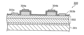
- FIG. 8 is a diagram showing a configuration of a conventional semiconductor element 300 described in Patent Document 1.
- a conventional semiconductor element 300 includes a substrate 301, a semiconductor layer stack 302, a first electrode 303a, a second electrode 303b, a first gate electrode 304a, and a second gate electrode 304b. Is provided.
- the semiconductor element 300 causes the power supply voltage to be reduced between the first electrode 303a and the second electrode 303b via the channel.
- a current can flow in a direction corresponding to the polarity.
- the conventional semiconductor device has a problem that power consumption increases.
- a first gate current flows from the first gate electrode toward the channel region immediately below the first gate electrode.
- a second gate current flows from the second gate electrode toward the channel region immediately below the second gate electrode.
- the potential of the second gate electrode is higher than the second electrode by the potential difference VGb between the second gate electrode and the second electrode, and higher than the first electrode by the sum of the power supply voltage VSba and the potential difference VGb. .
- the second gate current flows not only through the second electrode but also through the first electrode.
- the semiconductor device When the semiconductor device is in a conductive state and the power supply voltage VSba increases, the potential difference between the second gate electrode and the first electrode increases. For this reason, the second gate current increases as the power supply voltage VSba increases. Therefore, the driving power for driving the second gate electrode is increased.
- the present invention has been made to solve the above-described problems, and an object thereof is to provide a semiconductor device that can suppress an increase in power consumption and a driving method thereof.
- a semiconductor device is a semiconductor device including a semiconductor element that can flow a current bidirectionally, and the semiconductor element is formed over the substrate and the substrate And a pair of ohmic electrodes formed on or above the semiconductor layer and spaced apart from each other, and between the pair of ohmic electrodes on or above the semiconductor layer.
- a pair of gate electrodes corresponding to each of the pair of ohmic electrodes, and the semiconductor device further bi-directionally passes the semiconductor element between the pair of ohmic electrodes via the channel region.
- a control unit configured to make a conductive state in which a current can flow; and when the semiconductor element is in the conductive state, the control unit is configured to be a high one of the pair of ohmic electrodes.
- the potential of the high-potential side gate electrode which is a potential corresponding to the high-potential-side ohmic electrode
- a first electric signal is supplied to the high potential side gate electrode so as to be lower than the potential of the low potential side gate electrode which is a gate electrode corresponding to the low potential side ohmic electrode, and A second electric signal is supplied to the low potential side gate electrode.
- the magnitude of the gate current flowing through the high potential side gate electrode depends on the potential difference between the high potential side ohmic electrode and the high potential side gate electrode. Increase is suppressed and power consumption can be reduced.
- the magnitude of the saturation current of the current flowing between the pair of ohmic electrodes depends on the potential difference between the low-potential side ohmic electrode and the low-potential side gate electrode. The magnitude of the current can be maintained. Therefore, power consumption can be reduced while maintaining the characteristics of the power supply current and the power supply voltage.
- control unit includes a first voltage source that generates a first voltage that is equal to or higher than a threshold voltage of the pair of gate electrodes, and a second voltage source that generates a second voltage higher than the first voltage. And the control unit supplies the first voltage as the first electric signal to the high potential side gate electrode, and supplies the second voltage as the second electric signal to the low potential side gate electrode. Also good.
- a high voltage or a low voltage can be easily supplied between each gate electrode and the corresponding ohmic electrode. Accordingly, since the current flowing from the high potential side gate electrode to the channel region can be reduced while maintaining the characteristics of the power supply current and the power supply voltage, the driving power of the high potential side gate electrode can be suppressed.
- the control unit may include a first current source that generates a first current for applying a voltage that is equal to or higher than a threshold voltage of the pair of gate electrodes, and a second current that generates a second current larger than the first current. And the controller supplies the first current to the high potential side gate electrode as the first electrical signal and supplies the second current to the low potential side gate electrode as the second electrical signal. May be.
- the control unit may supply a current for applying a voltage equal to or higher than a threshold voltage of the pair of gate electrodes to the pair of gate electrodes as the first electric signal and the second electric signal.
- the threshold voltage of the pair of gate electrodes may be positive.
- the semiconductor element can be in a cut-off state.
- the semiconductor element may further include a pair of control layers having P-type conductivity formed between the pair of gate electrodes and the semiconductor layer.
- the threshold voltage of the first gate electrode and the threshold voltage of the second gate electrode can be made positive.
- the pair of gate electrodes may be in Schottky junction with the semiconductor layer.
- the threshold voltage of the first gate electrode and the threshold voltage of the second gate electrode can be made positive.
- the semiconductor element may further include an insulating film formed between the pair of gate electrodes and the semiconductor layer.
- the threshold voltage of the first gate electrode and the threshold voltage of the second gate electrode can be made positive.
- the substrate may be a silicon substrate, a sapphire substrate, or a silicon carbide substrate.
- a method for controlling a semiconductor device is a method for controlling a semiconductor device in which current can flow in both directions.
- the semiconductor device is formed over a substrate, the channel, and a channel.
- a pair of gate electrodes corresponding to each of the pair of ohmic electrodes, and the method of controlling the semiconductor device includes a high potential side gate which is a gate electrode corresponding to a high potential side ohmic electrode of the pair of ohmic electrodes
- a first electric signal is supplied to the electrode, and a second electric signal is applied to the low potential side gate electrode which is a gate electrode corresponding to the low potential side ohmic electrode of the pair of ohmic electrodes.
- the potential of the high potential side gate electrode when the high potential side ohmic electrode is used as a reference is the low potential side ohmic electrode
- the first electric signal and the second electric signal are supplied so as to be lower than the potential of the low-potential side gate electrode with reference to.
- the magnitude of the gate current flowing through the high potential side gate electrode depends on the potential difference between the high potential side ohmic electrode and the high potential side gate electrode. Increase is suppressed and power consumption can be reduced.
- the magnitude of the saturation current of the current flowing between the pair of ohmic electrodes depends on the potential difference between the low-potential side ohmic electrode and the low-potential side gate electrode. The magnitude of the current can be maintained. Therefore, power consumption can be reduced while maintaining the characteristics of the power supply current and the power supply voltage.
- the semiconductor device according to the present invention can suppress an increase in power consumption.
- FIG. 1A is a cross-sectional view showing an example of the configuration of the semiconductor device according to Embodiment 1 of the present invention.
- FIG. 1B is a cross-sectional view showing an example of the configuration of the semiconductor device according to Embodiment 1 of the present invention.
- FIG. 2 is a diagram for explaining the behavior of the channel region in the semiconductor device according to the first embodiment of the present invention.
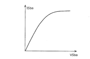
- FIG. 3A is a diagram showing an example of the relationship between the power supply current ISba and the power supply voltage VSba according to Embodiment 1 of the present invention.
- FIG. 3B is a diagram showing an example of the relationship between the gate current IGb and the power supply voltage VSba according to Embodiment 1 of the present invention.
- FIG. 4 is a cross-sectional view showing an example of the configuration of the semiconductor device according to the first modification of the first embodiment of the present invention.
- FIG. 5 is a cross-sectional view showing an example of the configuration of the semiconductor device according to Modification 2 of Embodiment 1 of the present invention.
- FIG. 6 is a cross-sectional view showing an example of the configuration of the semiconductor device according to the second embodiment of the present invention.
- FIG. 7 is a cross-sectional view showing an example of the configuration of a semiconductor device according to a variation of the second embodiment of the present invention.
- FIG. 8 is a cross-sectional view showing a configuration of a conventional semiconductor element.
- a semiconductor device includes a semiconductor element having a pair of gate electrodes and a pair of ohmic electrodes, and applying a voltage higher than a threshold voltage to the pair of gate electrodes. And a control unit for bringing the ohmic electrodes into a conductive state.
- the control unit applies a low voltage to the gate electrode corresponding to the high-potential side ohmic electrode and applies a high voltage to the gate electrode corresponding to the low-potential side ohmic electrode when the semiconductor element is in a conductive state. It is characterized by doing.
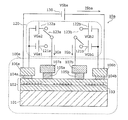
- FIGS. 1A and 1B are cross-sectional views showing an example of the configuration of the semiconductor device 10 according to the first embodiment of the present invention.
- the semiconductor device 10 includes a semiconductor element 100 and a control unit 120.
- the semiconductor element 100 can flow a current bidirectionally according to the polarity of the power supply voltage VSba of the power supply 130.
- a semiconductor element 100 includes a substrate 101, a semiconductor layer stack 102, a first ohmic electrode 104a, a second ohmic electrode 104b, a first gate electrode 105a, and a second gate.
- the electrode 105b, the first ohmic terminal 106a, the second ohmic terminal 106b, the first gate terminal 107a, the second gate terminal 107b, the first control layer 108a, and the second control layer 108b are provided.
- the substrate 101 is, for example, a semiconductor substrate such as silicon (Si).
- the substrate 101 may be a sapphire substrate or a silicon carbide (SiC) substrate.
- the semiconductor layer stack 102 is formed on the substrate 101 and has a channel region 103.
- the semiconductor layer stack 102 is made of, for example, GaN / AlGaN.
- the first ohmic electrode 104a and the second ohmic electrode 104b are a pair of ohmic electrodes formed on or above the semiconductor layer stack 102 so as to be separated from each other.
- the first ohmic electrode 104a and the second ohmic electrode 104b have, for example, a stacked structure of titanium (Ti) and aluminum (Al).
- the first gate electrode 105a is one of a pair of gate electrodes formed between the pair of ohmic electrodes on or above the semiconductor layer stack 102. Specifically, the first gate electrode 105a is formed between the first ohmic electrode 104a and the second ohmic electrode 104b.
- the first gate electrode 105a corresponds to one of a pair of ohmic electrodes. Specifically, the first gate electrode 105a corresponds to the first ohmic electrode 104a, and is formed in a region closer to the first ohmic electrode 104a than the second ohmic electrode 104b.
- the first gate electrode 105a is made of nickel (Ni), for example.
- the ohmic electrode and the gate electrode corresponding to the ohmic electrode are a pair of electrodes to which a voltage for forming a channel in the channel region 103 is applied.
- the first gate electrode 105a corresponding to the first ohmic electrode 104a is supplied with a potential higher than the threshold voltage of the first gate electrode 105a, which is a potential when the first ohmic electrode 104a is used as a reference. In this case, a channel is generated in the channel region 103 below the first gate electrode 105a.
- the threshold voltage of the first gate electrode 105a is positive, for example.
- the second gate electrode 105b is the other of the pair of gate electrodes formed between the pair of ohmic electrodes on or above the semiconductor layer stack 102. Specifically, the second gate electrode 105b is formed between the first gate electrode 105a and the second ohmic electrode 104b.
- the second gate electrode 105b corresponds to the other of the pair of ohmic electrodes. Specifically, the second gate electrode 105b corresponds to the second ohmic electrode 104b, and is formed in a region closer to the second ohmic electrode 104b than the first ohmic electrode 104a.
- the second gate electrode 105b is made of nickel, for example.
- the second gate electrode 105b corresponding to the second ohmic electrode 104b has a potential when the second ohmic electrode 104b is used as a reference and is equal to or higher than the threshold voltage of the second gate electrode 105b.
- a channel is generated in the channel region 103 below the second gate electrode 105b.
- the threshold voltage of the second gate electrode 105b is positive, for example.
- the first ohmic terminal 106a is connected to the first ohmic electrode 104a.
- the first ohmic terminal 106 a is a terminal for connecting a voltage source (or current source) included in the control unit 120 and the power source 130.
- the second ohmic terminal 106b is connected to the second ohmic electrode 104b.
- the second ohmic terminal 106 b is a terminal for connecting a voltage source (or current source) included in the control unit 120 and the power source 130.
- the first gate terminal 107a is connected to the first gate electrode 105a.
- the first gate terminal 107a is a terminal for connecting a voltage source (or current source) included in the control unit 120.
- the second gate terminal 107b is connected to the second gate electrode 105b.
- the second gate terminal 107b is a terminal for connecting a voltage source (or current source) included in the control unit 120.
- the first control layer 108a is a control layer having P-type conductivity formed between the first gate electrode 105a and the semiconductor layer stack 102.
- the first control layer 108a is made of, for example, P-GaN.
- the second control layer 108b is a control layer having P-type conductivity, which is formed between the second gate electrode 105b and the semiconductor layer stack 102.
- the second control layer 108b is made of, for example, P-GaN.
- Each of the first control layer 108 a and the second control layer 108 b forms a PN junction with the channel region 103.
- the control unit 120 is a circuit for bringing the semiconductor element 100 into a conductive state.
- the conduction state is a state in which a current can flow in both directions through the channel region 103 between the pair of ohmic electrodes (the first ohmic electrode 104a and the second ohmic electrode 104b).
- the control unit 120 includes voltage sources 121a, 121b, 122a and 122b, and switches 123a and 123b.
- the voltage source 121a is an example of a first voltage source that generates a first voltage that is equal to or higher than a threshold voltage of a pair of gate electrodes.
- the voltage source 121a is connected between the first ohmic terminal 106a and the first gate terminal 107a via a switch 123a.
- the voltage source 121a has a first potential that is the potential of the first gate electrode 105a when the first ohmic electrode 104a is used as a reference, so that the first potential is equal to or higher than the threshold voltage of the first gate electrode 105a.
- a gate voltage VGa1 is applied between the one gate electrode 105a and the first ohmic electrode 104a.
- the gate voltage VGa1 is an example of the first voltage, and is a voltage that is equal to or higher than the threshold voltage of the first gate electrode 105a.
- the voltage source 122a is an example of a second voltage source that generates a second voltage higher than the first voltage.
- the voltage source 121a is connected between the first ohmic terminal 106a and the first gate terminal 107a via a switch 123a.
- the voltage source 122a applies the gate voltage VGa2 between the first gate electrode 105a and the first ohmic electrode 104a so that the first potential is equal to or higher than the threshold voltage of the first gate electrode 105a.
- the gate voltage VGa2 is an example of a second voltage, which is equal to or higher than the threshold voltage of the first gate electrode 105a and higher than the gate voltage VGa1.
- the switch 123a selects either the voltage source 121a or the voltage source 122a according to the polarity of the power supply voltage VSba of the power supply 130. Specifically, the switch 123a has a high voltage when the power supply voltage VSba of the power supply 130 is positive, that is, when the potential of the second ohmic electrode 104b is higher than the potential of the first ohmic electrode 104a (see FIG. 1A). Source 122a is selected. Further, the switch 123a switches the low voltage source 121a when the power supply voltage VSba of the power supply 130 is negative, that is, when the potential of the second ohmic electrode 104b is lower than the potential of the first ohmic electrode 104a (see FIG. 1B). select.
- the voltage source 121b is an example of a first voltage source that generates a first voltage that is equal to or higher than a threshold voltage of a pair of gate electrodes.
- the voltage source 121b is connected between the second ohmic terminal 106b and the second gate terminal 107b via a switch 123b.
- the voltage source 121b is configured so that the second potential, which is the potential of the second gate electrode 105b with respect to the second ohmic electrode 104b, is equal to or higher than the threshold voltage of the second gate electrode 105b.
- a gate voltage VGb1 is applied between the two gate electrodes 105b and the second ohmic electrode 104b.
- the gate voltage VGb1 is an example of the first voltage, and is a voltage equal to or higher than the threshold voltage of the second gate electrode 105b. Further, the gate voltage VGb1 may be equal to the gate voltage VGa1.
- the voltage source 122b is an example of a second voltage source that generates a second voltage higher than the first voltage.
- the voltage source 121b is connected between the second ohmic terminal 106b and the second gate terminal 107b via a switch 123b.
- the voltage source 122b applies the gate voltage VGb2 between the second gate electrode 105b and the second ohmic electrode 104b so that the second potential is equal to or higher than the threshold voltage of the second gate electrode 105b.
- the gate voltage VGb2 is an example of a second voltage, which is equal to or higher than the threshold voltage of the second gate electrode 105b and higher than the gate voltage VGb1. Further, the gate voltage VGb2 may be equal to the gate voltage VGa2.
- the switch 123b selects either the voltage source 121b or the voltage source 122b according to the polarity of the power supply voltage VSba of the power supply 130. Specifically, the switch 123b has a low voltage when the power supply voltage VSba of the power supply 130 is positive, that is, when the potential of the second ohmic electrode 104b is higher than the potential of the first ohmic electrode 104a (see FIG. 1A). The source 121b is selected. Further, the switch 123b switches the high voltage source 122b when the power supply voltage VSba of the power supply 130 is negative, that is, when the potential of the second ohmic electrode 104b is lower than the potential of the first ohmic electrode 104a (see FIG. 1B). select.
- the control unit 120 has a potential when the high-potential-side ohmic electrode of the pair of ohmic electrodes is used as a reference, and the high-potential-side ohmic electrode.
- the potential of the high-potential-side gate electrode that is the corresponding gate electrode is a potential when the low-potential-side ohmic electrode is used as a reference, and the low-potential-side gate electrode that is the gate electrode corresponding to the low-potential-side ohmic electrode
- the first electric signal is supplied to the high potential side gate electrode and the second electric signal is supplied to the low potential side gate electrode so as to be lower than the first potential.
- the high-potential-side ohmic electrode and the high-potential-side gate electrode are the second ohmic electrode 104b and the second gate electrode 105b.
- the low potential side ohmic electrode and the low potential side gate electrode are the first ohmic electrode 104a and the first gate electrode 105a.
- the gate voltage VGb1 is supplied as a first electric signal from the low voltage source 121b to the second gate electrode 105b which is the high potential side gate electrode.
- the gate voltage VGa2 is supplied as the second electric signal from the high voltage source 122a to the first gate electrode 105a which is the low potential side gate electrode. At this time, VGa2> VGb1.
- the high-potential-side ohmic electrode and the high-potential-side gate electrode are the first ohmic electrode 104a and the first gate electrode 105a.
- the low potential side ohmic electrode and the low potential side gate electrode are the second ohmic electrode 104b and the second gate electrode 105b.
- the gate voltage VGa1 is supplied as a first electric signal from the low voltage source 121a to the first gate electrode 105a which is the high potential side gate electrode.
- the gate voltage VGb2 is supplied as a second electric signal from the high voltage source 122b to the second gate electrode 105b, which is the low potential side gate electrode. At this time, VGb2> VGa1.
- FIG. 2 is a diagram for explaining the behavior of the channel region 103 when the semiconductor element 100 according to the first embodiment of the present invention is in a conductive state.
- a potential VGa equal to or higher than the threshold voltage of the first gate electrode 105a is applied to the first gate electrode 105a with the first ohmic electrode 104a as a reference, and a potential VGb equal to or higher than the threshold voltage of the second gate electrode 105b is equal to the second ohmic.
- the semiconductor element 100 becomes conductive.
- a current ISba flows between the first ohmic electrode 104a and the second ohmic electrode 104b by applying the power supply voltage VSba between the first ohmic electrode 104a and the second ohmic electrode 104b.
- the direction of the current ISba is determined according to the polarity of the power supply voltage VSba. That is, of the first ohmic electrode 104a and the second ohmic electrode 104b, the current ISba flows from the high potential side ohmic electrode to the low potential side ohmic electrode.
- FIG. 3A is a diagram showing an example of the relationship between ISba and VSba according to Embodiment 1 of the present invention. As shown in FIG. 3A, as the power supply voltage VSba increases, the current ISba also increases.
- the potential of the first gate electrode 105a is higher by VGa than the potential of the first ohmic electrode 104a. Therefore, the first gate current IGa flows from the first gate electrode 105a to the channel region 103 through the first control layer 108a.
- the potential of the second gate electrode 105b is higher by VGb than the potential of the second ohmic electrode 104b, and higher by VSba + VGb than the potential of the first ohmic electrode 104a. Therefore, the second gate current IGb flows from the second gate electrode 105b to the channel region 103 through the second control layer 108b.
- Resistors 109 a, 109 b and 109 c exist inside the semiconductor element 100.
- the resistor 109a is a resistor from the first ohmic electrode 104a to the point A in the channel region immediately below the first gate electrode 105a.
- the resistor 109b is the resistance of the channel region from point A in the channel region immediately below the first gate electrode 105a to point B in the channel region immediately below the second gate electrode 105b.
- the resistor 109c is a resistor from the point B of the channel region immediately below the second gate electrode 105b to the second ohmic electrode 104b.
- the potential at point A in the channel region immediately below the first gate electrode 105a is higher than the potential at the first ohmic terminal 106a due to voltage drop caused by ISba and the resistor 109a. Since the potential at the point A rises as ISba increases, the voltage applied between the first gate electrode 105a and the point A becomes smaller than VGa as ISba increases.
- ISba When ISba further increases and no channel is formed at point A, ISba saturates as shown in FIG. 3A. Whether or not a channel is formed at the point A is determined by the potential difference between the point A and the first gate electrode 105a. Therefore, the potential of the first gate electrode 105a is high when the potential of the first ohmic electrode 104a is used as a reference. As a result, the channel at point A is more easily maintained.
- the magnitude of the saturation current of ISba depends on the magnitude of VGa. That is, the magnitude of the saturation current of ISba depends on the potential difference between the first gate electrode 105a and the first ohmic electrode 104a. In other words, the magnitude of the saturation current of ISba depends on the voltage applied between the low potential side ohmic electrode and the low potential side gate electrode.
- the potential at point B in the channel region immediately below the second gate electrode 105b is lower than the potential of the second ohmic terminal 106b due to voltage drop caused by ISba and the resistor 109c.
- the potential at the point B with respect to the second ohmic terminal 106b decreases as ISba increases.
- a voltage VGb is applied to the second gate terminal 107b with respect to the second ohmic terminal 106b.
- the voltage applied between the second gate electrode 105b and the point B increases with respect to VGb as ISba increases. Therefore, when the semiconductor element 100 is in a conductive state, when the potential VGb equal to or higher than the threshold voltage of the second gate electrode 105b is applied to the second gate electrode 105b with respect to the second ohmic electrode 104b, ISba increases. Even so, a channel is still formed at point B.
- the gate current IGb flowing through the second gate terminal 107b increases as the potential difference between the second gate electrode 105b and the second ohmic electrode 104b increases.
- the gate current flowing through the high potential side gate electrode increases as the potential difference between the high potential side gate electrode and the high potential side ohmic electrode increases.
- the potential at point B in the channel region immediately below the second gate electrode 105b is higher than the potential at the second ohmic terminal 106b due to voltage drop caused by ISba and the resistor 109c. Since the potential at the point B rises as ISba increases, the voltage applied between the second gate electrode 105b and the point B increases with respect to VGb as ISba increases.
- the magnitude of the saturation current of ISba depends on the magnitude of VGb. That is, the magnitude of the saturation current of ISba depends on the potential difference between the second gate electrode 105b and the second ohmic electrode 104b. In other words, the magnitude of the saturation current of ISba depends on the voltage applied between the low potential side ohmic electrode and the low potential side gate electrode.
- a voltage of VGa is applied to the first gate terminal 107a with respect to the first ohmic terminal 106a.
- the voltage applied between the first gate electrode 105a and the point A increases with respect to VGa as the absolute value of ISba increases. Therefore, when the semiconductor element 100 is in a conductive state, when a potential VGa that is equal to or higher than the threshold voltage of the first gate electrode 105a is applied to the first gate electrode 105a with respect to the first ohmic electrode 104a, the absolute value of ISba. Even if increases, a channel is still formed at point A.
- the magnitude of the ISba saturation current depends on the potential difference between the low potential side ohmic electrode and the low potential side gate electrode. Further, the magnitude of the gate current flowing through the high potential side gate electrode depends on the potential difference between the high potential side ohmic electrode and the high potential side gate electrode.
- the saturation current of ISba is increased.
- the gate current can be reduced while maintaining the thickness.
- the control unit 120 of the semiconductor device 10 includes two voltage sources 121a and 122a between the first ohmic terminal 106a and the first gate terminal 107a.
- the two voltage sources 121a and 122a generate gate voltages VGa1 (first voltage) and VGa2 (second voltage) that are equal to or higher than the threshold voltage of the first gate electrode 105a, respectively.
- the switch 123a selects one of the voltage sources 121a and 122a. That is, the switch 123a switches the voltage applied between the first ohmic terminal 106a and the first gate terminal 107a.
- VGa1 is equal to or higher than the threshold voltage of the first gate electrode 105a and lower than VGa2.
- the magnitude of VGa2 is set so that the saturation current of ISba can flow when VSba> 0.
- control unit 120 includes the voltage source 121a for low voltage and the voltage source 121b for high voltage, and selects a voltage to be applied to the first gate electrode 105a. That is, the control unit 120 can apply the low voltage VGa1 or the high voltage VGa2 to the first gate electrode 105a by the switch 123a.
- control unit 120 includes two voltage sources 121b and 122b between the second ohmic terminal 106b and the second gate terminal 107b.
- the two voltage sources 121b and 122b generate gate voltages VGb1 (first voltage) and VGb2 (second voltage) that are equal to or higher than the threshold voltage of the second gate electrode 105b, respectively.
- the switch 123b selects one of the voltage sources 121b and 122b. That is, the switch 123b switches the voltage applied between the second ohmic terminal 106b and the second gate terminal 107b.
- VGb1 is equal to or higher than the threshold voltage of the second gate electrode 105b and lower than VGb2.
- the magnitude of VGb2 is set so that the saturation current of ISba can flow when VSba ⁇ 0.
- VGa2 When VSba> 0, a high voltage VGa2 is applied between the low potential side first gate terminal 107a and the low potential side first ohmic terminal 106a.
- a voltage of VGb1 which is a low voltage, is applied between the second gate terminal 107b on the high potential side and the second ohmic terminal 106b on the high potential side.
- VGa2 that is a high voltage is between the first gate terminal 107a and the first ohmic terminal 106a, and a high voltage is between the second gate terminal 107b and the second ohmic terminal 106b.
- IGb can be suppressed.
- the characteristics of IGb and VSba are shown in FIG. 3B.
- the gate current IGb flowing from the second gate electrode 105b toward the channel region 103 increases as the potential difference between the second gate electrode 105b and the first ohmic electrode 104a increases.
- the potential difference between the second gate electrode 105b and the first ohmic electrode 104a is VSba + VGb2.
- the potential difference between the second gate electrode 105b and the first ohmic electrode 104a is VSba + VGb1.
- the saturation current of ISba depends on VGa2. Therefore, a high voltage VGa2 is provided between the first gate terminal 107a and the first ohmic terminal 106a, and a high voltage VGb2 is provided between the second gate terminal 107b and the second ohmic terminal 106b. Compared to the applied case, the saturation current of ISba does not decrease.
- a low voltage of VGa1 is applied between the first gate terminal 107a on the high potential side and the first ohmic terminal 106a on the high potential side.
- a high voltage VGb2 is applied between the low potential side second gate terminal 107b and the low potential side second ohmic terminal 106b.
- VGa2 that is a high voltage is between the first gate terminal 107a and the first ohmic terminal 106a, and a high voltage is between the second gate terminal 107b and the second ohmic terminal 106b.
- IGa can be suppressed.
- the saturation current of ISba depends on VGb2. Therefore, a high voltage VGa2 is provided between the first gate terminal 107a and the first ohmic terminal 106a, and a high voltage VGb2 is provided between the second gate terminal 107b and the second ohmic terminal 106b. Compared to the applied case, the saturation current of ISba does not decrease.
- the semiconductor device 10 applies the semiconductor element 100 having the pair of gate electrodes and the pair of ohmic electrodes, and a voltage equal to or higher than the threshold voltage to the pair of gate electrodes.
- a control unit 120 for bringing the semiconductor element 100 into a conductive state between the pair of ohmic electrodes.
- the control unit 120 applies a low voltage to the gate electrode corresponding to the high-potential side ohmic electrode and applies a high voltage to the gate electrode corresponding to the low-potential side ohmic electrode when the semiconductor element 100 is in a conductive state. Apply.
- the potential difference between the low-potential side ohmic electrode and the low-potential side gate electrode is maintained, while the high-potential side ohmic electrode and the high-potential side gate electrode are interposed. Reduce the potential difference.
- the magnitude of the saturation current of the current ISba flowing from the power supply 130 depends on the potential difference between the low potential side ohmic electrode and the low potential side gate electrode. Further, the magnitude of the gate current flowing through the high potential side gate electrode depends on the potential difference between the high potential side ohmic electrode and the high potential side gate electrode. For this reason, according to the semiconductor device 10 concerning Embodiment 1 of this invention, the magnitude
- the threshold voltages of the first gate electrode 105a and the second gate electrode 105b are both positive. Accordingly, the voltage applied to the first gate electrode 105a when the first ohmic electrode 104a is used as a reference and the voltage applied to the second gate electrode 105b when the second ohmic electrode 104b is used as a reference are both. When 0, the semiconductor element 100 can be cut off.
- FIG. 4 is a diagram showing an example of the configuration of the semiconductor device 10a according to the first modification of the first embodiment of the present invention. Constituent elements similar to those of the first embodiment are denoted by the same reference numerals, and the description thereof is omitted.
- the semiconductor device 10 a includes a semiconductor element 100 a instead of the semiconductor element 100.
- the semiconductor element 100a is different from the semiconductor element 100 in that the first control layer 108a and the second control layer 108b are not provided. That is, the first gate electrode 105a and the second gate electrode 105b and the semiconductor layer stack 102 are in Schottky junction. Even with such a configuration, while maintaining the characteristics of ISba-VSba, when VSba> 0, the increase in IGb, which is the gate current on the high potential side, is increased, and when VSba ⁇ 0, the gate current on the high potential side, IGA, is increased. Can be suppressed.
- the semiconductor device 10a according to the first modification of the first embodiment of the present invention similarly to the first embodiment, the decrease of the saturation current of the current ISba flowing from the power source is suppressed, and the gate current is reduced. By suppressing the increase, power consumption can be reduced.
- FIG. 5 is a diagram showing an example of the configuration of the semiconductor device 10b according to the second modification of the first embodiment of the present invention. Constituent elements similar to those of the first embodiment are denoted by the same reference numerals, and the description thereof is omitted.
- the semiconductor device 10 b according to the second modification of the first embodiment includes a semiconductor element 100 b instead of the semiconductor element 100.
- the semiconductor element 100b is different from the semiconductor element 100 in that the first insulating film 110a is provided instead of the first control layer 108a and the second insulating film 110b is provided instead of the second control layer 108b. ing.
- the first insulating film 110 a is an insulating film formed between the first gate electrode 105 a and the semiconductor layer stack 102.
- the second insulating film 110 b is an insulating film formed between the second gate electrode 105 b and the semiconductor layer stack 102.
- the first insulating film 110a and the second insulating film 110b are a silicon oxide film (SiO 2 ) or a silicon nitride film (SiN).
- the semiconductor element 100b is in a conductive state, and both IGa and IGb are 0 in a steady state.
- IGa and IGb flow transiently in order to accumulate the capacitance of the first gate electrode 105a and the capacitance of the second gate electrode 105b.
- transient IGb can be suppressed more than when VGb2 is applied.
- the decrease of the saturation current of the current ISba flowing from the power source is suppressed, and the gate current is reduced.
- the increase power consumption can be reduced.
- Embodiment 2 The semiconductor device according to Embodiment 2 of the present invention supplies a semiconductor element having a pair of gate electrodes and a pair of ohmic electrodes, and a current that becomes a voltage equal to or higher than a threshold voltage to the pair of gate electrodes. And a control unit for bringing the semiconductor element into a conductive state between the pair of ohmic electrodes.
- the control unit supplies a low current to the gate electrode corresponding to the high-potential side ohmic electrode and supplies a high current to the gate electrode corresponding to the low-potential side ohmic electrode when the semiconductor element is conductive. It is characterized by doing.
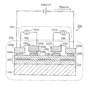
- FIG. 6 is a cross-sectional view showing an example of the configuration of the semiconductor device 20 according to the second embodiment of the present invention.
- the semiconductor device 20 includes a semiconductor element 100 and a control unit 140.
- the same components as those in the first embodiment are denoted by the same reference numerals, and the description thereof is omitted.
- the control unit 140 is a circuit for bringing the semiconductor element 100 into a conductive state. As shown in FIG. 6, the control unit 140 includes current sources 141a, 141b, 142a, and 142b, and switches 143a and 143b.
- the current source 141a is an example of a first current source that generates a first current for applying a voltage equal to or higher than a threshold voltage of a pair of gate electrodes.
- the current source 141a is connected between the first ohmic terminal 106a and the first gate terminal 107a via the switch 143a.
- the current source 141a is configured so that the first potential, which is the potential of the first gate electrode 105a with respect to the first ohmic electrode 104a, is equal to or higher than the threshold voltage of the first gate electrode 105a.
- a gate current IGa1 is supplied to one gate electrode 105a.
- the gate current IGa1 is an example of the first current.
- the current source 142a is an example of a second current source that generates a second current larger than the first current.
- the current source 142a is connected between the first ohmic terminal 106a and the first gate terminal 107a via the switch 143a.
- the current source 142a supplies the gate current IGa2 to the first gate electrode 105a so that the first potential is equal to or higher than the threshold voltage of the first gate electrode 105a.
- the gate current IGa2 is an example of the second current and is larger than the gate current IGa1.
- the switch 143a selects either the current source 141a or the current source 142a according to the polarity of the power supply voltage VSba of the power supply 130. Specifically, the switch 143a is a high-current current source when the power supply voltage VSba of the power supply 130 is positive, that is, when the potential of the second ohmic electrode 104b is higher than the potential of the first ohmic electrode 104a (FIG. 6). 142a is selected. The switch 143a selects the low-current current source 141a when the power supply voltage VSba of the power supply 130 is negative, that is, when the potential of the second ohmic electrode 104b is lower than the potential of the first ohmic electrode 104a.
- the current source 141b is an example of a first current source that generates a first current for applying a voltage equal to or higher than a threshold voltage of a pair of gate electrodes.
- the current source 141b is connected between the second ohmic terminal 106b and the second gate terminal 107b via a switch 143b.
- the current source 141b is configured so that the second potential, which is the potential of the second gate electrode 105b with respect to the second ohmic electrode 104b, is equal to or higher than the threshold voltage of the second gate electrode 105b.
- a gate current IGb1 is supplied to the two-gate electrode 105b.
- the gate current IGb1 is an example of the first current. Further, the gate current IGb1 may be equal to the gate current IGa1.
- the current source 142b is an example of a second current source that generates a second current larger than the first current.
- the current source 142b is connected between the second ohmic terminal 106b and the second gate terminal 107b via the switch 143b.
- the current source 142b supplies the gate current IGb2 to the second gate electrode 105b so that the second potential is equal to or higher than the threshold voltage of the second gate electrode 105b.
- the gate current IGb2 is an example of the second current and is larger than the gate current IGb1. Further, the gate current IGb2 may be equal to the gate current IGa2.
- the switch 143b selects either the current source 141b or the current source 142b according to the polarity of the power supply voltage VSba of the power supply 130. Specifically, the switch 143b is a low-current current source when the power supply voltage VSba of the power supply 130 is positive, that is, when the potential of the second ohmic electrode 104b is higher than the potential of the first ohmic electrode 104a (FIG. 6). 141b is selected. The switch 143b selects the high-current current source 142b when the power supply voltage VSba of the power supply 130 is negative, that is, when the potential of the second ohmic electrode 104b is lower than the potential of the first ohmic electrode 104a.
- the control unit 140 has a potential when the high-potential-side ohmic electrode is used as a reference and is applied to the high-potential-side ohmic electrode.
- the potential of the high-potential side gate electrode corresponding to the low-potential side ohmic electrode is the potential when the potential of the high-potential side gate electrode is based on the low-potential side ohmic electrode,
- the first electric signal is supplied to the high potential side gate electrode and the second electric signal is supplied to the low potential side gate electrode so as to be lower than the first potential.
- the high-potential-side ohmic electrode and the high-potential-side gate electrode are the second ohmic electrode 104b and the second gate electrode 105b.
- the low potential side ohmic electrode and the low potential side gate electrode are the first ohmic electrode 104a and the first gate electrode 105a.
- a gate current IGb1 is supplied as a first electric signal from the low current source 141b to the second gate electrode 105b which is the high potential side gate electrode. Then, the gate current IGa2 is supplied as the second electric signal from the high current source 142a to the first gate electrode 105a which is the low potential side gate electrode. At this time, IGa2> IGb1.
- the high potential side ohmic electrode and the high potential side gate electrode are the first ohmic electrode 104a and the first gate electrode 105a
- the low potential side ohmic electrode and the low potential side gate electrode are the second ohmic electrode.
- the gate electrode 104b and the second gate electrode 105b are used.
- the gate current IGa1 is supplied as the first electric signal from the low current source 141a to the first gate electrode 105a which is the high potential side gate electrode.
- the gate current IGb2 is supplied as the second electric signal from the high current source 142b to the second gate electrode 105b which is the low potential side gate electrode.
- IGb2 > IGa1.
- the control unit 140 of the semiconductor device 20 includes two current sources 141a and 142a between the first ohmic terminal 106a and the first gate terminal 107a.
- the two current sources 141a and 142a respectively generate gate currents IGa1 (first current) and IGa2 (second current) that can apply a potential equal to or higher than the threshold voltage of the first gate electrode 105a.
- the switch 143a selects one of the current sources 141a and 142a. That is, the switch 143a switches the current supplied to the first gate terminal 107a.
- IGa1 is a current for applying a voltage equal to or higher than the threshold voltage of the first gate electrode 105a, and is a current smaller than IGa2.
- the magnitude of IGa2 is set so as to be a gate voltage VGa that allows a saturation current of ISba to flow when VSba> 0.
- control unit 140 includes the current source 141a for low current and the current source 142a for high current, and selects the current to be supplied to the first gate electrode 105a. That is, the control unit 140 can supply IGa1 having a low current or IGa2 having a high current to the first gate electrode 105a by the switch 143a.
- control unit 140 includes two current sources 141b and 142b between the second ohmic terminal 106b and the second gate terminal 107b.
- the two current sources 141b and 142b generate gate currents IGb1 (first current) and IGb2 (second current) that can apply a potential higher than the threshold voltage of the second gate electrode 105b, respectively.
- the switch 143b selects one of the current sources 141b and 142b. That is, the switch 143b switches the current supplied to the second gate terminal 107b.
- IGb1 is a current for applying a voltage equal to or higher than the threshold voltage of the second gate electrode 105b, and is a current smaller than IGb2. Further, the magnitude of IGb2 is set to be a gate voltage VGb that allows a saturation current of ISba to flow when VSba ⁇ 0.
- control unit 140 includes the current source 141b for low current and the current source 142b for high current, and selects the current to be supplied to the second gate electrode 105b. That is, the control unit 140 can supply IGb1 having a low current or IGb2 having a high current to the second gate electrode 105b by the switch 143b.
- IGb1 smaller than IGb2 is supplied to the second gate terminal 107b on the high potential side. Then, the high current IGa2 is supplied to the first gate terminal 107a on the low potential side. Even in this state, a channel is generated in the channel region 103 immediately below the second gate terminal 107b. Accordingly, the driving power of the second gate terminal 107b is reduced.
- IGa1 smaller than IGa2 is supplied to the first gate terminal 107a on the high potential side.
- IGb2 which is a high current, is supplied to the second gate terminal 107b on the low potential side. Even in this state, a channel is generated in the channel region 103 immediately below the second gate terminal 107b. Accordingly, the driving power of the first gate terminal 107a can be suppressed.
- the semiconductor element 100 having the pair of gate electrodes and the pair of ohmic electrodes and the pair of gate electrodes have a voltage equal to or higher than the threshold voltage.
- a control unit 140 is provided that brings the semiconductor element 100 into a conductive state between the pair of ohmic electrodes by supplying a current.
- the control unit 140 supplies a low current to the gate electrode corresponding to the high-potential side ohmic electrode and supplies a high current to the gate electrode corresponding to the low-potential side ohmic electrode when the semiconductor element 100 is conductive. Supply.
- FIG. 7 is a diagram showing an example of the configuration of the semiconductor device 20a according to the variation of the second embodiment of the present invention. Constituent elements similar to those of the second embodiment are denoted by the same reference numerals, and the description thereof is omitted.
- the semiconductor device 20 a includes a control unit 150 instead of the control unit 140.
- the control unit 150 includes current sources 151a and 151b.
- the current source 151a is an example of a current source that generates a current for applying a voltage higher than the threshold voltage of the pair of gate electrodes.
- the current source 151a is connected between the first ohmic terminal 106a and the first gate terminal 107a.
- the current source 151a supplies the gate current IGa as the first electric signal to the first gate terminal 107a.
- the current source 151b is an example of a current source that generates a current for applying a voltage higher than the threshold voltage of the pair of gate electrodes.
- the current source 151b is connected between the second ohmic terminal 106b and the second gate terminal 107b.
- the current source 151b supplies the gate current IGb as the second electric signal to the second gate terminal 107b.
- both IGa and IGb are currents for applying a voltage higher than the threshold voltage of the gate electrode.
- IGa and IGb each have the same current value.
- the decrease of the saturation current of the current ISba flowing from the power source is suppressed and the increase of the gate current is increased. By suppressing the power consumption, power consumption can be reduced.
- the semiconductor device is a semiconductor device including a semiconductor element capable of flowing a current bidirectionally, and the semiconductor element includes a substrate, A semiconductor layer having a channel region formed on the substrate, a pair of ohmic electrodes formed on or above the semiconductor layer and spaced apart from each other, and the pair of ohmics on or above the semiconductor layer And a pair of gate electrodes corresponding to each of the pair of ohmic electrodes formed between the electrodes, and the semiconductor device further includes the semiconductor element and the channel region between the pair of ohmic electrodes.
- a control unit configured to make a conductive state in which a current can flow in both directions through the pair of ohmics when the semiconductor element is in the conductive state.
- the potential when the high potential side ohmic electrode is used as a reference, and the potential of the high potential side gate electrode corresponding to the high potential side ohmic electrode is the same as that of the low potential side ohmic electrode.
- the first electric signal is supplied to the high potential side gate electrode so as to be lower than the potential of the low potential side gate electrode, which is the potential of the reference and is the gate electrode corresponding to the low potential side ohmic electrode.
- a second electric signal is supplied to the low potential side gate electrode.
- the magnitude of the gate current flowing through the high potential side gate electrode depends on the potential difference between the high potential side ohmic electrode and the high potential side gate electrode. Increase is suppressed and power consumption can be reduced.
- the magnitude of the saturation current of the current flowing between the pair of ohmic electrodes depends on the potential difference between the low-potential side ohmic electrode and the low-potential side gate electrode. The magnitude of the current can be maintained. Therefore, power consumption can be reduced while maintaining the characteristics of the power supply current and the power supply voltage.
- control unit includes a first voltage source that generates a first voltage that is equal to or higher than a threshold voltage of the pair of gate electrodes, and a second voltage source that generates a second voltage higher than the first voltage. And the control unit supplies the first voltage as the first electric signal to the high potential side gate electrode, and supplies the second voltage as the second electric signal to the low potential side gate electrode. Also good.
- a high voltage or a low voltage can be easily supplied between each gate electrode and the corresponding ohmic electrode. Accordingly, since the current flowing from the high potential side gate electrode to the channel region can be reduced while maintaining the characteristics of the power supply current and the power supply voltage, the driving power of the high potential side gate electrode can be suppressed.
- the control unit may include a first current source that generates a first current for applying a voltage that is equal to or higher than a threshold voltage of the pair of gate electrodes, and a second current that generates a second current larger than the first current. And the controller supplies the first current to the high potential side gate electrode as the first electrical signal and supplies the second current to the low potential side gate electrode as the second electrical signal. May be.
- the control unit may supply a current for applying a voltage equal to or higher than a threshold voltage of the pair of gate electrodes to the pair of gate electrodes as the first electric signal and the second electric signal.
- the threshold voltage of the pair of gate electrodes may be positive.
- the semiconductor element can be in a cut-off state.
- the semiconductor element may further include a pair of control layers having P-type conductivity formed between the pair of gate electrodes and the semiconductor layer.
- the threshold voltage of the first gate electrode and the threshold voltage of the second gate electrode can be made positive.
- the pair of gate electrodes may be in Schottky junction with the semiconductor layer.
- the threshold voltage of the first gate electrode and the threshold voltage of the second gate electrode can be made positive.
- the semiconductor element may further include an insulating film formed between the pair of gate electrodes and the semiconductor layer.
- the threshold voltage of the first gate electrode and the threshold voltage of the second gate electrode can be made positive.
- the substrate may be a silicon substrate, a sapphire substrate, or a silicon carbide substrate.
- a method for controlling a semiconductor device is a method for controlling a semiconductor device capable of flowing a current in both directions.
- the semiconductor device is formed on a substrate and the substrate, A semiconductor layer having a channel region, a pair of ohmic electrodes formed on or above the semiconductor layer and spaced apart from each other, and formed between the pair of ohmic electrodes on or above the semiconductor layer
- a pair of gate electrodes corresponding to each of the pair of ohmic electrodes, and the method of controlling the semiconductor device is a high potential side which is a gate electrode corresponding to a high potential side ohmic electrode of the pair of ohmic electrodes
- a first electrical signal is supplied to the gate electrode, and a second potential is applied to the low potential side gate electrode that is a gate electrode corresponding to the low potential side ohmic electrode of the pair of ohmic electrodes.
- the potential of the high-potential-side gate electrode when the high-potential-side ohmic electrode is used as a reference is the low-potential-side ohmic
- the first electric signal and the second electric signal are supplied so as to be lower than the potential of the low potential side gate electrode when the electrode is used as a reference.
- the magnitude of the gate current flowing through the high potential side gate electrode depends on the potential difference between the high potential side ohmic electrode and the high potential side gate electrode. Increase is suppressed and power consumption can be reduced.
- the magnitude of the saturation current of the current flowing between the pair of ohmic electrodes depends on the potential difference between the low-potential side ohmic electrode and the low-potential side gate electrode. The magnitude of the current can be maintained. Therefore, power consumption can be reduced while maintaining the characteristics of the power supply current and the power supply voltage.
- the semiconductor device and the control method thereof according to the present invention have been described based on the embodiments, but the present invention is not limited to these embodiments. Unless it deviates from the meaning of this invention, the form which carried out the various deformation
- the control unit 120 applies the high voltage VGa2 generated by the voltage source 122a between the first gate electrode 105a and the first ohmic electrode 104a when the high-potential-side ohmic electrode is the second ohmic electrode 104b.
- the low voltage VGa1 generated by the voltage source 121a may be applied between the second gate electrode 105b and the second ohmic electrode 104b.
- the control unit 120 applies the low voltage VGa1 generated by the voltage source 121a between the first gate electrode 105a and the first ohmic electrode 104a.
- the high voltage VGa2 generated by the voltage source 122a may be applied between the second gate electrode 105b and the second ohmic electrode 104b.
- the control unit 140 supplies the high current IGa2 generated by the current source 142a to the first gate electrode 105a, and generates the low current generated by the current source 141a.
- the current IGa1 may be supplied to the second gate electrode 105b.
- the control unit 140 supplies the low current IGa2 generated by the current source 141a to the first gate electrode 105a, and generates a high current generated by the current source 142a.
- the current IGa1 may be supplied to the second gate electrode 105b.
- the configuration of the semiconductor device is for illustration in order to specifically describe the present invention, and the semiconductor device according to the present invention is not necessarily provided with all of the above configurations. In other words, the semiconductor device according to the present invention need only have a minimum configuration capable of realizing the effects of the present invention.
- the first ohmic terminal 106a, the second ohmic terminal 106b, the first gate terminal 107a, and the second gate terminal 107b may not be provided.
- the semiconductor device and the control method thereof according to the present invention have an effect that an increase in power consumption can be suppressed.
Abstract
Disclosed is a semiconductor device (10), which is provided with a semiconductor element (100) that can bidirectionally flow a current. The semiconductor element (100) is provided with a pair of a first ohmic electrode (104a) and a second ohmic electrode (104b), and a pair of a first gate electrode (105a) and a second gate electrode (105b). The semiconductor device (10) is also provided with a control unit (120), which brings the semiconductor element (100) into an electrically connected state. The control unit (120) supplies a first electric signal to a high potential-side gate electrode, and supplies a second electric signal to a low potential-side gate electrode, such that, in the case where the semiconductor element (100) is electrically connected, the potential of the high potential-side gate electrode, said potential corresponding to a high potential-side ohmic electrode with the high potential-side ohmic electrode as reference, is lower than the potential of the low potential-side gate electrode, said potential corresponding to the low potential-side ohmic electrode with the low potential-side ohmic electrode as reference.
Description
本発明は、半導体装置及びその制御方法に関し、特に、双方向に電流を流すことができる半導体素子を備える半導体装置及びその制御方法に関する。
The present invention relates to a semiconductor device and a control method thereof, and more particularly, to a semiconductor device including a semiconductor element capable of flowing a current bidirectionally and a control method thereof.
近年、材料限界を打破して導通損失を低減するために、GaNに代表されるIII族窒化物半導体又は炭化珪素(SiC)などのワイドギャップ半導体を用いた半導体装置の導入が検討されている。ワイドギャップ半導体は、絶縁破壊電界がシリコン(Si)と比べて約1桁高い。
In recent years, in order to overcome material limitations and reduce conduction loss, introduction of a semiconductor device using a wide gap semiconductor such as a group III nitride semiconductor represented by GaN or silicon carbide (SiC) has been studied. A wide gap semiconductor has a dielectric breakdown electric field about an order of magnitude higher than that of silicon (Si).
窒化アルミニウムガリウム(AlGaN)と窒化ガリウム(GaN)とのヘテロ接合界面には、自発分極及びピエゾ分極により電荷が生じる。これにより、アンドープ時においても1×1013cm-2以上のシートキャリア濃度と、1000cm2V/sec以上の高移動度の2次元電子ガス(2DEG)層が形成される。このため、AlGaN/GaNヘテロ接合電界効果トランジスタ(AlGaN/GaN-HFET)は、低オン抵抗及び高耐圧を実現するパワースイッチングトランジスタとして期待されている。
Electric charges are generated at the heterojunction interface between aluminum gallium nitride (AlGaN) and gallium nitride (GaN) due to spontaneous polarization and piezoelectric polarization. As a result, a sheet carrier concentration of 1 × 10 13 cm −2 or more and a high mobility two-dimensional electron gas (2DEG) layer of 1000 cm 2 V / sec or more are formed even when undoped. Therefore, the AlGaN / GaN heterojunction field effect transistor (AlGaN / GaN-HFET) is expected as a power switching transistor that realizes low on-resistance and high breakdown voltage.
特に、AlGaN/GaNのヘテロ接合を利用して2つのゲート電極を有する構造にすることにより、1つの半導体装置で双方向半導体装置を形成することが可能となる(例えば、特許文献1を参照)。
In particular, by using a structure having two gate electrodes using an AlGaN / GaN heterojunction, a bidirectional semiconductor device can be formed with a single semiconductor device (see, for example, Patent Document 1). .
図8は、特許文献1に記載の従来の半導体素子300の構成を示す図である。図8に示すように、従来の半導体素子300は、基板301と、半導体層積層体302と、第1電極303aと、第2電極303bと、第1ゲート電極304aと、第2ゲート電極304bとを備える。
FIG. 8 is a diagram showing a configuration of a conventional semiconductor element 300 described in Patent Document 1. In FIG. As shown in FIG. 8, a conventional semiconductor element 300 includes a substrate 301, a semiconductor layer stack 302, a first electrode 303a, a second electrode 303b, a first gate electrode 304a, and a second gate electrode 304b. Is provided.
第1ゲート電極304aと第2ゲート電極304bとにそれぞれ、閾値電圧より高い電圧が印加された場合、半導体層積層体302にチャネルが生成される。これにより、半導体素子300は、第1電極303aと第2電極303bとの間で、チャネルを介して導通状態となる。
When a voltage higher than the threshold voltage is applied to each of the first gate electrode 304a and the second gate electrode 304b, a channel is generated in the semiconductor layer stack 302. As a result, the semiconductor element 300 becomes conductive between the first electrode 303a and the second electrode 303b via the channel.
これにより、第1電極303aと第2電極303bとの間に電源電圧が印加された場合、半導体素子300は、第1電極303aと第2電極303bとの間でチャネルを介して、電源電圧の極性に応じた方向に電流を流すことができる。
As a result, when a power supply voltage is applied between the first electrode 303a and the second electrode 303b, the semiconductor element 300 causes the power supply voltage to be reduced between the first electrode 303a and the second electrode 303b via the channel. A current can flow in a direction corresponding to the polarity.
しかしながら、上記従来の半導体装置では、消費電力が増大してしまうという課題がある。
However, the conventional semiconductor device has a problem that power consumption increases.
従来の半導体素子が導通状態にあるとき、第1ゲート電極から第1ゲート電極直下のチャネル領域に向かって第1ゲート電流が流れる。同様に、第2ゲート電極から第2ゲート電極直下のチャネル領域に向かって第2ゲート電流が流れる。
When the conventional semiconductor element is in a conductive state, a first gate current flows from the first gate electrode toward the channel region immediately below the first gate electrode. Similarly, a second gate current flows from the second gate electrode toward the channel region immediately below the second gate electrode.
ここで、第2ゲート電極の電位は、第2電極よりも、第2ゲート電極と第2電極との間の電位差VGbだけ高く、第1電極よりも電源電圧VSbaと電位差VGbとの和だけ高い。このため、第2ゲート電流は、第2電極だけでなく、第1電極にも流れる。
Here, the potential of the second gate electrode is higher than the second electrode by the potential difference VGb between the second gate electrode and the second electrode, and higher than the first electrode by the sum of the power supply voltage VSba and the potential difference VGb. . For this reason, the second gate current flows not only through the second electrode but also through the first electrode.
半導体装置が導通状態であり電源電圧VSbaが高くなると、第2ゲート電極と第1電極との電位差が増加する。このため、電源電圧VSbaの上昇に伴って、第2ゲート電流は高くなる。したがって、第2ゲート電極を駆動する駆動電力が大きくなってしまう。
When the semiconductor device is in a conductive state and the power supply voltage VSba increases, the potential difference between the second gate electrode and the first electrode increases. For this reason, the second gate current increases as the power supply voltage VSba increases. Therefore, the driving power for driving the second gate electrode is increased.
そこで、本発明は、上記課題を解決するためになされたものであって、消費電力の増大を抑制することができる半導体装置及びその駆動方法を提供することを目的とする。
Therefore, the present invention has been made to solve the above-described problems, and an object thereof is to provide a semiconductor device that can suppress an increase in power consumption and a driving method thereof.
上記課題を解決するため、本発明の一態様に係る半導体装置は、双方向に電流を流すことができる半導体素子を備える半導体装置であって、前記半導体素子は、基板と、前記基板上に形成され、チャネル領域を有する半導体層と、前記半導体層の上又は上方に、互いに離隔して形成された一対のオーミック電極と、前記半導体層の上又は上方に、前記一対のオーミック電極の間に形成された、前記一対のオーミック電極のそれぞれに対応する一対のゲート電極とを備え、前記半導体装置は、さらに、前記半導体素子を、前記一対のオーミック電極の間で前記チャネル領域を介して双方向に電流を流すことが可能な導通状態にする制御部を備え、前記制御部は、前記半導体素子が前記導通状態である場合、前記一対のオーミック電極のうち高電位側のオーミック電極を基準とした場合の電位であって、前記高電位側のオーミック電極に対応するゲート電極である高電位側ゲート電極の電位が、低電位側のオーミック電極を基準とした場合の電位であって、前記低電位側のオーミック電極に対応するゲート電極である低電位側ゲート電極の電位より低くなるように、前記高電位側ゲート電極に第1電気信号を供給し、かつ、前記低電位側ゲート電極に第2電気信号を供給する。
In order to solve the above problems, a semiconductor device according to one embodiment of the present invention is a semiconductor device including a semiconductor element that can flow a current bidirectionally, and the semiconductor element is formed over the substrate and the substrate And a pair of ohmic electrodes formed on or above the semiconductor layer and spaced apart from each other, and between the pair of ohmic electrodes on or above the semiconductor layer. A pair of gate electrodes corresponding to each of the pair of ohmic electrodes, and the semiconductor device further bi-directionally passes the semiconductor element between the pair of ohmic electrodes via the channel region. A control unit configured to make a conductive state in which a current can flow; and when the semiconductor element is in the conductive state, the control unit is configured to be a high one of the pair of ohmic electrodes. When the potential of the high-potential side gate electrode, which is a potential corresponding to the high-potential-side ohmic electrode, is based on the low-potential-side ohmic electrode A first electric signal is supplied to the high potential side gate electrode so as to be lower than the potential of the low potential side gate electrode which is a gate electrode corresponding to the low potential side ohmic electrode, and A second electric signal is supplied to the low potential side gate electrode.
これにより、高電位側ゲート電極に流れるゲート電流の大きさは、高電位側のオーミック電極と高電位側ゲート電極との間の電位差に依存するので、当該電位差を低くすることで、ゲート電流の増大が抑制され、消費電力を削減することができる。また、一対のオーミック電極間を流れる電流の飽和電流の大きさは、低電位側のオーミック電極と低電位側のゲート電極との間の電位差に依存するので、当該電位差を高くすることで、飽和電流の大きさを保つことができる。したがって、電源電流と電源電圧との特性を維持したまま、消費電力を削減することができる。
As a result, the magnitude of the gate current flowing through the high potential side gate electrode depends on the potential difference between the high potential side ohmic electrode and the high potential side gate electrode. Increase is suppressed and power consumption can be reduced. In addition, the magnitude of the saturation current of the current flowing between the pair of ohmic electrodes depends on the potential difference between the low-potential side ohmic electrode and the low-potential side gate electrode. The magnitude of the current can be maintained. Therefore, power consumption can be reduced while maintaining the characteristics of the power supply current and the power supply voltage.
また、前記制御部は、前記一対のゲート電極の閾値電圧以上の電圧である第1電圧を生成する第1電圧源と、前記第1電圧より高い第2電圧を生成する第2電圧源とを有し、前記制御部は、前記高電位側ゲート電極に前記第1電圧を前記第1電気信号として供給し、前記低電位側ゲート電極に前記第2電圧を前記第2電気信号として供給してもよい。
Further, the control unit includes a first voltage source that generates a first voltage that is equal to or higher than a threshold voltage of the pair of gate electrodes, and a second voltage source that generates a second voltage higher than the first voltage. And the control unit supplies the first voltage as the first electric signal to the high potential side gate electrode, and supplies the second voltage as the second electric signal to the low potential side gate electrode. Also good.
これにより、異なる電圧を発生する2つの電圧源を備えることで、各ゲート電極と、対応するオーミック電極との間に高電圧又は低電圧を容易に供給することができる。したがって、電源電流と電源電圧との特性を維持したまま、高電位側ゲート電極からチャネル領域に流れる電流を低減することができるため、高電位側ゲート電極の駆動電力を抑制することができる。
Thus, by providing two voltage sources that generate different voltages, a high voltage or a low voltage can be easily supplied between each gate electrode and the corresponding ohmic electrode. Accordingly, since the current flowing from the high potential side gate electrode to the channel region can be reduced while maintaining the characteristics of the power supply current and the power supply voltage, the driving power of the high potential side gate electrode can be suppressed.
また、前記制御部は、前記一対のゲート電極の閾値電圧以上の電圧を印加するための第1電流を生成する第1電流源と、前記第1電流より大きい第2電流を生成する第2電流源とを備え、前記制御部は、前記高電位側ゲート電極に前記第1電流を前記第1電気信号として供給し、前記低電位側ゲート電極に前記第2電流を前記第2電気信号として供給してもよい。
The control unit may include a first current source that generates a first current for applying a voltage that is equal to or higher than a threshold voltage of the pair of gate electrodes, and a second current that generates a second current larger than the first current. And the controller supplies the first current to the high potential side gate electrode as the first electrical signal and supplies the second current to the low potential side gate electrode as the second electrical signal. May be.
これにより、異なる電流を発生する2つの電流源を備えることで、各ゲート電極に高電流又は低電流を容易に供給することができる。したがって、電源電流と電源電圧との特性を維持したまま、高電位側のゲート電流を低減し、高電位側ゲート電極の駆動電力を抑制することができる。
Thereby, by providing two current sources that generate different currents, a high current or a low current can be easily supplied to each gate electrode. Therefore, it is possible to reduce the high-potential-side gate current and suppress the driving power of the high-potential-side gate electrode while maintaining the characteristics of the power supply current and the power supply voltage.
また、前記制御部は、前記一対のゲート電極の閾値電圧以上の電圧を印加するための電流を、前記第1電気信号及び前記第2電気信号として前記一対のゲート電極に供給してもよい。
The control unit may supply a current for applying a voltage equal to or higher than a threshold voltage of the pair of gate electrodes to the pair of gate electrodes as the first electric signal and the second electric signal.
これにより、第1ゲート電極又は第2ゲート電極に供給するゲート電流源の数を減らすことができ、回路構成を簡素化することができる。
Thereby, the number of gate current sources supplied to the first gate electrode or the second gate electrode can be reduced, and the circuit configuration can be simplified.
また、前記一対のゲート電極の閾値電圧は、正であってもよい。
Further, the threshold voltage of the pair of gate electrodes may be positive.
これにより、第1オーミック電極を基準とした場合に第1ゲート電極に印加される電圧、及び、第2オーミック電極を基準とした場合に第2ゲート電極に印加される電圧がともに0のときに、半導体素子を遮断状態とすることができる。
Thus, when the voltage applied to the first gate electrode when the first ohmic electrode is used as a reference and the voltage applied to the second gate electrode when the second ohmic electrode is used as a reference are both zero. The semiconductor element can be in a cut-off state.
また、前記半導体素子は、さらに、前記一対のゲート電極と前記半導体層との間に形成された、P型の導電性を有する一対のコントロール層を備えてもよい。
The semiconductor element may further include a pair of control layers having P-type conductivity formed between the pair of gate electrodes and the semiconductor layer.
これにより、第1ゲート電極の閾値電圧及び第2ゲート電極の閾値電圧を正にすることができる。
Thereby, the threshold voltage of the first gate electrode and the threshold voltage of the second gate electrode can be made positive.
また、前記一対のゲート電極は、前記半導体層とショットキー接合していてもよい。
The pair of gate electrodes may be in Schottky junction with the semiconductor layer.
これにより、第1ゲート電極の閾値電圧及び第2ゲート電極の閾値電圧を正にすることができる。
Thereby, the threshold voltage of the first gate electrode and the threshold voltage of the second gate electrode can be made positive.
また、前記半導体素子は、さらに、前記一対のゲート電極と前記半導体層との間に形成された絶縁膜を備えてもよい。
The semiconductor element may further include an insulating film formed between the pair of gate electrodes and the semiconductor layer.
これにより、第1ゲート電極の閾値電圧及び第2ゲート電極の閾値電圧を正にすることができる。
Thereby, the threshold voltage of the first gate electrode and the threshold voltage of the second gate electrode can be made positive.
また、前記基板は、シリコン基板、サファイア基板、又は、炭化珪素基板であってもよい。
The substrate may be a silicon substrate, a sapphire substrate, or a silicon carbide substrate.
また、本発明の一態様に係る半導体装置の制御方法は、双方向に電流を流すことができる半導体装置の制御方法であって、前記半導体装置は、基板と、前記基板上に形成され、チャネル領域を有する半導体層と、前記半導体層の上又は上方に、互いに離隔して形成された一対のオーミック電極と、前記半導体層の上又は上方に、前記一対のオーミック電極の間に形成された、前記一対のオーミック電極のそれぞれに対応する一対のゲート電極とを備え、前記半導体装置の制御方法は、前記一対のオーミック電極のうち高電位側のオーミック電極に対応するゲート電極である高電位側ゲート電極に第1電気信号を供給し、前記一対のオーミック電極のうち低電位側のオーミック電極に対応するゲート電極である低電位側ゲート電極に第2電気信号を供給し、前記第1電気信号及び前記第2電気信号の供給では、前記高電位側のオーミック電極を基準とした場合の前記高電位側ゲート電極の電位が、前記低電位側のオーミック電極を基準とした場合の前記低電位側ゲート電極の電位より低くなるように、前記第1電気信号及び前記第2電気信号を供給する。
In addition, a method for controlling a semiconductor device according to one embodiment of the present invention is a method for controlling a semiconductor device in which current can flow in both directions. The semiconductor device is formed over a substrate, the channel, and a channel. A semiconductor layer having a region; a pair of ohmic electrodes formed on or above the semiconductor layer; and formed between the pair of ohmic electrodes on or above the semiconductor layer; A pair of gate electrodes corresponding to each of the pair of ohmic electrodes, and the method of controlling the semiconductor device includes a high potential side gate which is a gate electrode corresponding to a high potential side ohmic electrode of the pair of ohmic electrodes A first electric signal is supplied to the electrode, and a second electric signal is applied to the low potential side gate electrode which is a gate electrode corresponding to the low potential side ohmic electrode of the pair of ohmic electrodes. In the supply of the first electric signal and the second electric signal, the potential of the high potential side gate electrode when the high potential side ohmic electrode is used as a reference is the low potential side ohmic electrode The first electric signal and the second electric signal are supplied so as to be lower than the potential of the low-potential side gate electrode with reference to.
これにより、高電位側ゲート電極に流れるゲート電流の大きさは、高電位側のオーミック電極と高電位側ゲート電極との間の電位差に依存するので、当該電位差を低くすることで、ゲート電流の増大が抑制され、消費電力を削減することができる。また、一対のオーミック電極間を流れる電流の飽和電流の大きさは、低電位側のオーミック電極と低電位側のゲート電極との間の電位差に依存するので、当該電位差を高くすることで、飽和電流の大きさを保つことができる。したがって、電源電流と電源電圧との特性を維持したまま、消費電力を削減することができる。
As a result, the magnitude of the gate current flowing through the high potential side gate electrode depends on the potential difference between the high potential side ohmic electrode and the high potential side gate electrode. Increase is suppressed and power consumption can be reduced. In addition, the magnitude of the saturation current of the current flowing between the pair of ohmic electrodes depends on the potential difference between the low-potential side ohmic electrode and the low-potential side gate electrode. The magnitude of the current can be maintained. Therefore, power consumption can be reduced while maintaining the characteristics of the power supply current and the power supply voltage.
本発明に係る半導体装置によれば、消費電力の増加を抑制することができる。
The semiconductor device according to the present invention can suppress an increase in power consumption.
以下では、本発明の実施の形態に係る半導体装置及びその制御方法について、図面を用いて詳細に説明する。なお、以下に示す実施の形態は例示を目的としており、本発明がこれらに限定されることを意図しない。
Hereinafter, a semiconductor device and a control method thereof according to an embodiment of the present invention will be described in detail with reference to the drawings. The following embodiments are for illustrative purposes and are not intended to limit the present invention.
(実施の形態1)
本発明の実施の形態1に係る半導体装置は、一対のゲート電極と一対のオーミック電極とを有する半導体素子と、一対のゲート電極に閾値電圧以上の電圧を印加することで、半導体素子を一対のオーミック電極間で導通状態にする制御部とを備える。そして、制御部は、半導体素子が導通状態である場合に、高電位側のオーミック電極に対応するゲート電極に低電圧を印加し、低電位側のオーミック電極に対応するゲート電極に高電圧を印加することを特徴とする。 (Embodiment 1)
A semiconductor device according toEmbodiment 1 of the present invention includes a semiconductor element having a pair of gate electrodes and a pair of ohmic electrodes, and applying a voltage higher than a threshold voltage to the pair of gate electrodes. And a control unit for bringing the ohmic electrodes into a conductive state. The control unit applies a low voltage to the gate electrode corresponding to the high-potential side ohmic electrode and applies a high voltage to the gate electrode corresponding to the low-potential side ohmic electrode when the semiconductor element is in a conductive state. It is characterized by doing.
本発明の実施の形態1に係る半導体装置は、一対のゲート電極と一対のオーミック電極とを有する半導体素子と、一対のゲート電極に閾値電圧以上の電圧を印加することで、半導体素子を一対のオーミック電極間で導通状態にする制御部とを備える。そして、制御部は、半導体素子が導通状態である場合に、高電位側のオーミック電極に対応するゲート電極に低電圧を印加し、低電位側のオーミック電極に対応するゲート電極に高電圧を印加することを特徴とする。 (Embodiment 1)
A semiconductor device according to
図1A及び図1Bは、本発明の実施の形態1に係る半導体装置10の構成の一例を示す断面図である。図1A及び図1Bに示すように、半導体装置10は、半導体素子100と、制御部120とを備える。半導体素子100は、電源130の電源電圧VSbaの極性に応じて、双方向に電流を流すことができる。
1A and 1B are cross-sectional views showing an example of the configuration of the semiconductor device 10 according to the first embodiment of the present invention. As illustrated in FIGS. 1A and 1B, the semiconductor device 10 includes a semiconductor element 100 and a control unit 120. The semiconductor element 100 can flow a current bidirectionally according to the polarity of the power supply voltage VSba of the power supply 130.
図1A及び図1Bに示すように、半導体素子100は、基板101と、半導体層積層体102と、第1オーミック電極104aと、第2オーミック電極104bと、第1ゲート電極105aと、第2ゲート電極105bと、第1オーミック端子106aと、第2オーミック端子106bと、第1ゲート端子107aと、第2ゲート端子107bと、第1コントロール層108aと、第2コントロール層108bとを備える。
As shown in FIGS. 1A and 1B, a semiconductor element 100 includes a substrate 101, a semiconductor layer stack 102, a first ohmic electrode 104a, a second ohmic electrode 104b, a first gate electrode 105a, and a second gate. The electrode 105b, the first ohmic terminal 106a, the second ohmic terminal 106b, the first gate terminal 107a, the second gate terminal 107b, the first control layer 108a, and the second control layer 108b are provided.
基板101は、例えば、シリコン(Si)などの半導体基板である。基板101は、サファイア基板又は炭化珪素(SiC)基板でもよい。
The substrate 101 is, for example, a semiconductor substrate such as silicon (Si). The substrate 101 may be a sapphire substrate or a silicon carbide (SiC) substrate.
半導体層積層体102は、基板101の上に形成され、チャネル領域103を有する。半導体層積層体102は、例えば、GaN/AlGaNから構成される。
The semiconductor layer stack 102 is formed on the substrate 101 and has a channel region 103. The semiconductor layer stack 102 is made of, for example, GaN / AlGaN.
第1オーミック電極104a及び第2オーミック電極104bは、半導体層積層体102の上又は上方に、互いに離隔して形成された一対のオーミック電極である。第1オーミック電極104a及び第2オーミック電極104bは、例えば、チタン(Ti)とアルミニウム(Al)との積層構造を有する。
The first ohmic electrode 104a and the second ohmic electrode 104b are a pair of ohmic electrodes formed on or above the semiconductor layer stack 102 so as to be separated from each other. The first ohmic electrode 104a and the second ohmic electrode 104b have, for example, a stacked structure of titanium (Ti) and aluminum (Al).
第1ゲート電極105aは、半導体層積層体102の上又は上方に、一対のオーミック電極の間に形成された一対のゲート電極の一方である。具体的には、第1ゲート電極105aは、第1オーミック電極104aと第2オーミック電極104bとの間に形成されている。
The first gate electrode 105a is one of a pair of gate electrodes formed between the pair of ohmic electrodes on or above the semiconductor layer stack 102. Specifically, the first gate electrode 105a is formed between the first ohmic electrode 104a and the second ohmic electrode 104b.
また、第1ゲート電極105aは、一対のオーミック電極の一方に対応している。具体的には、第1ゲート電極105aは、第1オーミック電極104aに対応し、第2オーミック電極104bより第1オーミック電極104aに近い領域に形成されている。第1ゲート電極105aは、例えば、ニッケル(Ni)で構成される。
The first gate electrode 105a corresponds to one of a pair of ohmic electrodes. Specifically, the first gate electrode 105a corresponds to the first ohmic electrode 104a, and is formed in a region closer to the first ohmic electrode 104a than the second ohmic electrode 104b. The first gate electrode 105a is made of nickel (Ni), for example.
なお、オーミック電極と、当該オーミック電極に対応するゲート電極とは、チャネル領域103にチャネルを形成するための電圧を印加するペアとなる電極である。具体的には、第1オーミック電極104aに対応する第1ゲート電極105aに、第1オーミック電極104aを基準とした場合の電位であって、第1ゲート電極105aの閾値電圧以上の電位が供給された場合に、第1ゲート電極105aの下方のチャネル領域103にチャネルが生成される。なお、第1ゲート電極105aの閾値電圧は、例えば、正である。
Note that the ohmic electrode and the gate electrode corresponding to the ohmic electrode are a pair of electrodes to which a voltage for forming a channel in the channel region 103 is applied. Specifically, the first gate electrode 105a corresponding to the first ohmic electrode 104a is supplied with a potential higher than the threshold voltage of the first gate electrode 105a, which is a potential when the first ohmic electrode 104a is used as a reference. In this case, a channel is generated in the channel region 103 below the first gate electrode 105a. Note that the threshold voltage of the first gate electrode 105a is positive, for example.
第2ゲート電極105bは、半導体層積層体102の上又は上方に、一対のオーミック電極の間に形成された一対のゲート電極の他方である。具体的には、第2ゲート電極105bは、第1ゲート電極105aと第2オーミック電極104bとの間に形成されている。
The second gate electrode 105b is the other of the pair of gate electrodes formed between the pair of ohmic electrodes on or above the semiconductor layer stack 102. Specifically, the second gate electrode 105b is formed between the first gate electrode 105a and the second ohmic electrode 104b.
また、第2ゲート電極105bは、一対のオーミック電極の他方に対応している。具体的には、第2ゲート電極105bは、第2オーミック電極104bに対応し、第1オーミック電極104aより第2オーミック電極104bに近い領域に形成されている。第2ゲート電極105bは、例えば、ニッケルで構成される。
The second gate electrode 105b corresponds to the other of the pair of ohmic electrodes. Specifically, the second gate electrode 105b corresponds to the second ohmic electrode 104b, and is formed in a region closer to the second ohmic electrode 104b than the first ohmic electrode 104a. The second gate electrode 105b is made of nickel, for example.
また、第2オーミック電極104bに対応する第2ゲート電極105bに、第2オーミック電極104bを基準とした場合の電位であって、第2ゲート電極105bの閾値電圧以上の電位が供給された場合に、第2ゲート電極105bの下方のチャネル領域103にチャネルが生成される。なお、第2ゲート電極105bの閾値電圧は、例えば、正である。
In addition, when the second gate electrode 105b corresponding to the second ohmic electrode 104b has a potential when the second ohmic electrode 104b is used as a reference and is equal to or higher than the threshold voltage of the second gate electrode 105b. A channel is generated in the channel region 103 below the second gate electrode 105b. Note that the threshold voltage of the second gate electrode 105b is positive, for example.
第1オーミック端子106aは、第1オーミック電極104aと接続されている。第1オーミック端子106aは、制御部120が備える電圧源(又は電流源)、及び、電源130の接続用の端子である。
The first ohmic terminal 106a is connected to the first ohmic electrode 104a. The first ohmic terminal 106 a is a terminal for connecting a voltage source (or current source) included in the control unit 120 and the power source 130.
第2オーミック端子106bは、第2オーミック電極104bと接続されている。第2オーミック端子106bは、制御部120が備える電圧源(又は電流源)、及び、電源130の接続用の端子である。
The second ohmic terminal 106b is connected to the second ohmic electrode 104b. The second ohmic terminal 106 b is a terminal for connecting a voltage source (or current source) included in the control unit 120 and the power source 130.
第1ゲート端子107aは、第1ゲート電極105aと接続されている。第1ゲート端子107aは、制御部120が備える電圧源(又は電流源)の接続用の端子である。
The first gate terminal 107a is connected to the first gate electrode 105a. The first gate terminal 107a is a terminal for connecting a voltage source (or current source) included in the control unit 120.
第2ゲート端子107bは、第2ゲート電極105bと接続されている。第2ゲート端子107bは、制御部120が備える電圧源(又は電流源)の接続用の端子である。
The second gate terminal 107b is connected to the second gate electrode 105b. The second gate terminal 107b is a terminal for connecting a voltage source (or current source) included in the control unit 120.
第1コントロール層108aは、第1ゲート電極105aと半導体層積層体102との間に形成された、P型の導電性を持つコントロール層である。第1コントロール層108aは、例えば、P-GaNから構成される。
The first control layer 108a is a control layer having P-type conductivity formed between the first gate electrode 105a and the semiconductor layer stack 102. The first control layer 108a is made of, for example, P-GaN.
第2コントロール層108bは、第2ゲート電極105bと半導体層積層体102との間に形成された、P型の導電性を持つコントロール層である。第2コントロール層108bは、例えば、P-GaNから構成される。第1コントロール層108a及び第2コントロール層108bはそれぞれ、チャネル領域103との間でPN接合を形成している。
The second control layer 108b is a control layer having P-type conductivity, which is formed between the second gate electrode 105b and the semiconductor layer stack 102. The second control layer 108b is made of, for example, P-GaN. Each of the first control layer 108 a and the second control layer 108 b forms a PN junction with the channel region 103.
制御部120は、半導体素子100を導通状態にするための回路である。導通状態とは、一対のオーミック電極(第1オーミック電極104aと第2オーミック電極104b)の間でチャネル領域103を介して双方向に電流を流すことが可能な状態である。図1A及び図1Bに示すように、制御部120は、電圧源121a、121b、122a及び122bと、スイッチ123a及び123bとを備える。
The control unit 120 is a circuit for bringing the semiconductor element 100 into a conductive state. The conduction state is a state in which a current can flow in both directions through the channel region 103 between the pair of ohmic electrodes (the first ohmic electrode 104a and the second ohmic electrode 104b). As shown in FIGS. 1A and 1B, the control unit 120 includes voltage sources 121a, 121b, 122a and 122b, and switches 123a and 123b.
電圧源121aは、一対のゲート電極の閾値電圧以上の電圧である第1電圧を生成する第1電圧源の一例である。電圧源121aは、第1オーミック端子106aと第1ゲート端子107aとの間に、スイッチ123aを介して接続されている。
The voltage source 121a is an example of a first voltage source that generates a first voltage that is equal to or higher than a threshold voltage of a pair of gate electrodes. The voltage source 121a is connected between the first ohmic terminal 106a and the first gate terminal 107a via a switch 123a.
具体的には、電圧源121aは、第1オーミック電極104aを基準とした場合の第1ゲート電極105aの電位である第1電位が、第1ゲート電極105aの閾値電圧以上となるように、第1ゲート電極105aと第1オーミック電極104aとの間にゲート電圧VGa1を印加する。なお、ゲート電圧VGa1は、第1電圧の一例であり、第1ゲート電極105aの閾値電圧以上の電圧である。
Specifically, the voltage source 121a has a first potential that is the potential of the first gate electrode 105a when the first ohmic electrode 104a is used as a reference, so that the first potential is equal to or higher than the threshold voltage of the first gate electrode 105a. A gate voltage VGa1 is applied between the one gate electrode 105a and the first ohmic electrode 104a. The gate voltage VGa1 is an example of the first voltage, and is a voltage that is equal to or higher than the threshold voltage of the first gate electrode 105a.
電圧源122aは、第1電圧より高い第2電圧を生成する第2電圧源の一例である。電圧源121aは、第1オーミック端子106aと第1ゲート端子107aとの間に、スイッチ123aを介して接続されている。
The voltage source 122a is an example of a second voltage source that generates a second voltage higher than the first voltage. The voltage source 121a is connected between the first ohmic terminal 106a and the first gate terminal 107a via a switch 123a.
具体的には、電圧源122aは、第1電位が第1ゲート電極105aの閾値電圧以上となるように、第1ゲート電極105aと第1オーミック電極104aとの間にゲート電圧VGa2を印加する。なお、ゲート電圧VGa2は、第2電圧の一例であり、第1ゲート電極105aの閾値電圧以上であり、かつ、ゲート電圧VGa1より高い電圧である。
Specifically, the voltage source 122a applies the gate voltage VGa2 between the first gate electrode 105a and the first ohmic electrode 104a so that the first potential is equal to or higher than the threshold voltage of the first gate electrode 105a. Note that the gate voltage VGa2 is an example of a second voltage, which is equal to or higher than the threshold voltage of the first gate electrode 105a and higher than the gate voltage VGa1.
スイッチ123aは、電源130の電源電圧VSbaの極性に応じて、電圧源121a及び電圧源122aのいずれかを選択する。具体的には、スイッチ123aは、電源130の電源電圧VSbaが正の場合、すなわち、第2オーミック電極104bの電位が第1オーミック電極104aの電位より高い場合(図1A参照)、高電圧の電圧源122aを選択する。また、スイッチ123aは、電源130の電源電圧VSbaが負の場合、すなわち、第2オーミック電極104bの電位が第1オーミック電極104aの電位より低い場合(図1B参照)、低電圧の電圧源121aを選択する。
The switch 123a selects either the voltage source 121a or the voltage source 122a according to the polarity of the power supply voltage VSba of the power supply 130. Specifically, the switch 123a has a high voltage when the power supply voltage VSba of the power supply 130 is positive, that is, when the potential of the second ohmic electrode 104b is higher than the potential of the first ohmic electrode 104a (see FIG. 1A). Source 122a is selected. Further, the switch 123a switches the low voltage source 121a when the power supply voltage VSba of the power supply 130 is negative, that is, when the potential of the second ohmic electrode 104b is lower than the potential of the first ohmic electrode 104a (see FIG. 1B). select.
電圧源121bは、一対のゲート電極の閾値電圧以上の電圧である第1電圧を生成する第1電圧源の一例である。電圧源121bは、第2オーミック端子106bと第2ゲート端子107bとの間に、スイッチ123bを介して接続されている。
The voltage source 121b is an example of a first voltage source that generates a first voltage that is equal to or higher than a threshold voltage of a pair of gate electrodes. The voltage source 121b is connected between the second ohmic terminal 106b and the second gate terminal 107b via a switch 123b.
具体的には、電圧源121bは、第2オーミック電極104bを基準とした場合の第2ゲート電極105bの電位である第2電位が、第2ゲート電極105bの閾値電圧以上となるように、第2ゲート電極105bと第2オーミック電極104bとの間にゲート電圧VGb1を印加する。なお、ゲート電圧VGb1は、第1電圧の一例であり、第2ゲート電極105bの閾値電圧以上の電圧である。また、ゲート電圧VGb1は、ゲート電圧VGa1と等しくてもよい。
Specifically, the voltage source 121b is configured so that the second potential, which is the potential of the second gate electrode 105b with respect to the second ohmic electrode 104b, is equal to or higher than the threshold voltage of the second gate electrode 105b. A gate voltage VGb1 is applied between the two gate electrodes 105b and the second ohmic electrode 104b. Note that the gate voltage VGb1 is an example of the first voltage, and is a voltage equal to or higher than the threshold voltage of the second gate electrode 105b. Further, the gate voltage VGb1 may be equal to the gate voltage VGa1.
電圧源122bは、第1電圧より高い第2電圧を生成する第2電圧源の一例である。電圧源121bは、第2オーミック端子106bと第2ゲート端子107bとの間に、スイッチ123bを介して接続されている。
The voltage source 122b is an example of a second voltage source that generates a second voltage higher than the first voltage. The voltage source 121b is connected between the second ohmic terminal 106b and the second gate terminal 107b via a switch 123b.
具体的には、電圧源122bは、第2電位が第2ゲート電極105bの閾値電圧以上となるように、第2ゲート電極105bと第2オーミック電極104bとの間にゲート電圧VGb2を印加する。なお、ゲート電圧VGb2は、第2電圧の一例であり、第2ゲート電極105bの閾値電圧以上であり、かつ、ゲート電圧VGb1より高い電圧である。また、ゲート電圧VGb2は、ゲート電圧VGa2と等しくてもよい。
Specifically, the voltage source 122b applies the gate voltage VGb2 between the second gate electrode 105b and the second ohmic electrode 104b so that the second potential is equal to or higher than the threshold voltage of the second gate electrode 105b. Note that the gate voltage VGb2 is an example of a second voltage, which is equal to or higher than the threshold voltage of the second gate electrode 105b and higher than the gate voltage VGb1. Further, the gate voltage VGb2 may be equal to the gate voltage VGa2.
スイッチ123bは、電源130の電源電圧VSbaの極性に応じて、電圧源121b及び電圧源122bのいずれかを選択する。具体的には、スイッチ123bは、電源130の電源電圧VSbaが正の場合、すなわち、第2オーミック電極104bの電位が第1オーミック電極104aの電位より高い場合(図1A参照)、低電圧の電圧源121bを選択する。また、スイッチ123bは、電源130の電源電圧VSbaが負の場合、すなわち、第2オーミック電極104bの電位が第1オーミック電極104aの電位より低い場合(図1B参照)、高電圧の電圧源122bを選択する。
The switch 123b selects either the voltage source 121b or the voltage source 122b according to the polarity of the power supply voltage VSba of the power supply 130. Specifically, the switch 123b has a low voltage when the power supply voltage VSba of the power supply 130 is positive, that is, when the potential of the second ohmic electrode 104b is higher than the potential of the first ohmic electrode 104a (see FIG. 1A). The source 121b is selected. Further, the switch 123b switches the high voltage source 122b when the power supply voltage VSba of the power supply 130 is negative, that is, when the potential of the second ohmic electrode 104b is lower than the potential of the first ohmic electrode 104a (see FIG. 1B). select.
このように、制御部120は、半導体素子100を導通状態にする場合に、一対のオーミック電極のうち高電位側のオーミック電極を基準とした場合の電位であって、高電位側のオーミック電極に対応するゲート電極である高電位側ゲート電極の電位が、低電位側のオーミック電極を基準とした場合の電位であって、低電位側のオーミック電極に対応するゲート電極である低電位側ゲート電極の電位より低くなるように、高電位側ゲート電極に第1電気信号を供給し、かつ、低電位側ゲート電極に第2電気信号を供給する。
As described above, when the semiconductor element 100 is brought into the conductive state, the control unit 120 has a potential when the high-potential-side ohmic electrode of the pair of ohmic electrodes is used as a reference, and the high-potential-side ohmic electrode. The potential of the high-potential-side gate electrode that is the corresponding gate electrode is a potential when the low-potential-side ohmic electrode is used as a reference, and the low-potential-side gate electrode that is the gate electrode corresponding to the low-potential-side ohmic electrode The first electric signal is supplied to the high potential side gate electrode and the second electric signal is supplied to the low potential side gate electrode so as to be lower than the first potential.
例えば、図1Aの例では、高電位側のオーミック電極及び高電位側ゲート電極は、第2オーミック電極104b及び第2ゲート電極105bである。そして、低電位側のオーミック電極及び低電位側ゲート電極は、第1オーミック電極104a及び第1ゲート電極105aである。
For example, in the example of FIG. 1A, the high-potential-side ohmic electrode and the high-potential-side gate electrode are the second ohmic electrode 104b and the second gate electrode 105b. The low potential side ohmic electrode and the low potential side gate electrode are the first ohmic electrode 104a and the first gate electrode 105a.
高電位側ゲート電極である第2ゲート電極105bには、低電圧の電圧源121bからゲート電圧VGb1が第1電気信号として供給される。そして、低電位側ゲート電極である第1ゲート電極105aには、高電圧の電圧源122aからゲート電圧VGa2が第2電気信号として供給される。このとき、VGa2>VGb1である。
The gate voltage VGb1 is supplied as a first electric signal from the low voltage source 121b to the second gate electrode 105b which is the high potential side gate electrode. The gate voltage VGa2 is supplied as the second electric signal from the high voltage source 122a to the first gate electrode 105a which is the low potential side gate electrode. At this time, VGa2> VGb1.
図1Bの例では、高電位側のオーミック電極及び高電位側ゲート電極は、第1オーミック電極104a及び第1ゲート電極105aである。そして、低電位側のオーミック電極及び低電位側ゲート電極は、第2オーミック電極104b及び第2ゲート電極105bである。
In the example of FIG. 1B, the high-potential-side ohmic electrode and the high-potential-side gate electrode are the first ohmic electrode 104a and the first gate electrode 105a. The low potential side ohmic electrode and the low potential side gate electrode are the second ohmic electrode 104b and the second gate electrode 105b.
高電位側ゲート電極である第1ゲート電極105aには、低電圧の電圧源121aからゲート電圧VGa1が第1電気信号として供給される。そして、低電位側ゲート電極である第2ゲート電極105bには、高電圧の電圧源122bからゲート電圧VGb2が第2電気信号として供給される。このとき、VGb2>VGa1である。
The gate voltage VGa1 is supplied as a first electric signal from the low voltage source 121a to the first gate electrode 105a which is the high potential side gate electrode. The gate voltage VGb2 is supplied as a second electric signal from the high voltage source 122b to the second gate electrode 105b, which is the low potential side gate electrode. At this time, VGb2> VGa1.
以下では、本発明の実施の形態1に係る半導体装置10の動作について説明する。
Hereinafter, the operation of the semiconductor device 10 according to the first embodiment of the present invention will be described.
図2は、本発明の実施の形態1に係る半導体素子100が導通状態である場合におけるチャネル領域103の挙動を説明するための図である。
FIG. 2 is a diagram for explaining the behavior of the channel region 103 when the semiconductor element 100 according to the first embodiment of the present invention is in a conductive state.
第1ゲート電極105aの閾値電圧以上の電位VGaが、第1オーミック電極104aを基準として第1ゲート電極105aに印加され、かつ、第2ゲート電極105bの閾値電圧以上の電位VGbが、第2オーミック電極104bを基準として第2ゲート電極105bに印加された場合に、半導体素子100は導電状態となる。このとき、第1オーミック電極104aと第2オーミック電極104bとの間に、電源電圧VSbaを印加することで、第1オーミック電極104aと第2オーミック電極104bとの間に電流ISbaが流れる。
A potential VGa equal to or higher than the threshold voltage of the first gate electrode 105a is applied to the first gate electrode 105a with the first ohmic electrode 104a as a reference, and a potential VGb equal to or higher than the threshold voltage of the second gate electrode 105b is equal to the second ohmic. When applied to the second gate electrode 105b with the electrode 104b as a reference, the semiconductor element 100 becomes conductive. At this time, a current ISba flows between the first ohmic electrode 104a and the second ohmic electrode 104b by applying the power supply voltage VSba between the first ohmic electrode 104a and the second ohmic electrode 104b.
このとき、電流ISbaの向きは、電源電圧VSbaの極性に応じて決定される。つまり、第1オーミック電極104aと第2オーミック電極104bとのうち、高電位側のオーミック電極から低電位側のオーミック電極に電流ISbaが流れる。
At this time, the direction of the current ISba is determined according to the polarity of the power supply voltage VSba. That is, of the first ohmic electrode 104a and the second ohmic electrode 104b, the current ISba flows from the high potential side ohmic electrode to the low potential side ohmic electrode.
図3Aは、本発明の実施の形態1に係るISbaとVSbaとの関係の一例を示す図である。図3Aに示すように、電源電圧VSbaが大きくなるにつれて、電流ISbaも大きくなる。
FIG. 3A is a diagram showing an example of the relationship between ISba and VSba according to Embodiment 1 of the present invention. As shown in FIG. 3A, as the power supply voltage VSba increases, the current ISba also increases.
また、半導体素子100が導通状態であるとき、第1ゲート電極105aの電位は、第1オーミック電極104aの電位よりVGaだけ高い。したがって、第1ゲート電極105aから第1コントロール層108aを介してチャネル領域103へ第1ゲート電流IGaが流れる。
Further, when the semiconductor element 100 is in a conductive state, the potential of the first gate electrode 105a is higher by VGa than the potential of the first ohmic electrode 104a. Therefore, the first gate current IGa flows from the first gate electrode 105a to the channel region 103 through the first control layer 108a.
同様に、半導体素子100が導通状態であるとき、第2ゲート電極105bの電位は、第2オーミック電極104bの電位よりVGbだけ高く、第1オーミック電極104aの電位よりVSba+VGbだけ高い。したがって、第2ゲート電極105bから第2コントロール層108bを介してチャネル領域103へ第2ゲート電流IGbが流れる。
Similarly, when the semiconductor element 100 is in a conductive state, the potential of the second gate electrode 105b is higher by VGb than the potential of the second ohmic electrode 104b, and higher by VSba + VGb than the potential of the first ohmic electrode 104a. Therefore, the second gate current IGb flows from the second gate electrode 105b to the channel region 103 through the second control layer 108b.
まず、VSba>0の場合(図1A)について説明する。第1ゲート電極105a直下のチャネル領域103について、半導体素子100が導通状態のとき、高電位側の第2オーミック電極104bから低電位側の第1オーミック電極104aに向けて、チャネル領域103には電流ISbaが流れている。
First, the case where VSba> 0 (FIG. 1A) will be described. With respect to the channel region 103 immediately below the first gate electrode 105a, when the semiconductor element 100 is in a conductive state, the channel region 103 has a current flowing from the second ohmic electrode 104b on the high potential side toward the first ohmic electrode 104a on the low potential side. ISba is flowing.
半導体素子100の内部には、抵抗109a、109b及び109cが存在する。抵抗109aは、第1オーミック電極104aから第1ゲート電極105a直下のチャネル領域のA点までの抵抗である。抵抗109bは、第1ゲート電極105a直下のチャネル領域のA点から第2ゲート電極105b直下のチャネル領域のB点までのチャネル領域の抵抗である。抵抗109cは、第2ゲート電極105b直下のチャネル領域のB点から第2オーミック電極104bまでの抵抗である。
Resistors 109 a, 109 b and 109 c exist inside the semiconductor element 100. The resistor 109a is a resistor from the first ohmic electrode 104a to the point A in the channel region immediately below the first gate electrode 105a. The resistor 109b is the resistance of the channel region from point A in the channel region immediately below the first gate electrode 105a to point B in the channel region immediately below the second gate electrode 105b. The resistor 109c is a resistor from the point B of the channel region immediately below the second gate electrode 105b to the second ohmic electrode 104b.
半導体素子100が導通状態で、ISbaが流れると抵抗109a、109b及び109cで、それぞれ電圧ドロップが発生する。各電圧ドロップの総和が、電源電圧VSbaに相当する。
When the semiconductor element 100 is in a conductive state and ISba flows, a voltage drop occurs in each of the resistors 109a, 109b, and 109c. The total sum of the voltage drops corresponds to the power supply voltage VSba.
第1ゲート電極105a直下のチャネル領域のA点の電位は、ISbaと抵抗109aとによる電圧ドロップにより、第1オーミック端子106aの電位よりも高くなっている。A点の電位は、ISbaの増加に伴って上昇するため、第1ゲート電極105aとA点との間に印加される電圧は、ISbaが増加するほどVGaに対して小さくなる。
The potential at point A in the channel region immediately below the first gate electrode 105a is higher than the potential at the first ohmic terminal 106a due to voltage drop caused by ISba and the resistor 109a. Since the potential at the point A rises as ISba increases, the voltage applied between the first gate electrode 105a and the point A becomes smaller than VGa as ISba increases.
ISbaがさらに増加し、A点にチャネルが形成されなくなった時点で、図3Aに示すように、ISbaは飽和する。A点にチャネルが形成されるか否かは、A点と第1ゲート電極105aとの電位差によって決まるので、第1オーミック電極104aの電位を基準とした場合の第1ゲート電極105aの電位が高い程、A点のチャネルは維持されやすくなる。
When ISba further increases and no channel is formed at point A, ISba saturates as shown in FIG. 3A. Whether or not a channel is formed at the point A is determined by the potential difference between the point A and the first gate electrode 105a. Therefore, the potential of the first gate electrode 105a is high when the potential of the first ohmic electrode 104a is used as a reference. As a result, the channel at point A is more easily maintained.
したがって、ISbaの飽和電流の大きさは、VGaの大きさに依存する。つまり、ISbaの飽和電流の大きさは、第1ゲート電極105aと第1オーミック電極104aとの電位差に依存する。言い換えると、ISbaの飽和電流の大きさは、低電位側のオーミック電極と低電位側ゲート電極との間に印加される電圧に依存する。
Therefore, the magnitude of the saturation current of ISba depends on the magnitude of VGa. That is, the magnitude of the saturation current of ISba depends on the potential difference between the first gate electrode 105a and the first ohmic electrode 104a. In other words, the magnitude of the saturation current of ISba depends on the voltage applied between the low potential side ohmic electrode and the low potential side gate electrode.
なお、ISbaが増加するとA点の電位が上昇するため、第1ゲート端子107aから第1ゲート電極105a及び第1コントロール層108aを介してチャネル領域103に流れる電流IGaは減少する。
Note that, as ISba increases, the potential at point A increases, so that the current IGa flowing from the first gate terminal 107a to the channel region 103 via the first gate electrode 105a and the first control layer 108a decreases.
次に、第2ゲート電極105b直下のチャネル領域103について説明すると、半導体素子100が導通状態のとき、チャネル領域103にはISbaが流れる。
Next, the channel region 103 immediately below the second gate electrode 105b will be described. When the semiconductor element 100 is conductive, ISba flows through the channel region 103.
第2ゲート電極105b直下のチャネル領域のB点の電位は、ISbaと抵抗109cとによる電圧ドロップにより、第2オーミック端子106bの電位よりも低くなっている。第2オーミック端子106bに対するB点の電位は、ISbaの増加に伴って下降する。
The potential at point B in the channel region immediately below the second gate electrode 105b is lower than the potential of the second ohmic terminal 106b due to voltage drop caused by ISba and the resistor 109c. The potential at the point B with respect to the second ohmic terminal 106b decreases as ISba increases.
また、第2ゲート端子107bには、第2オーミック端子106bに対してVGbの電圧が印加されている。第2ゲート電極105bとB点との間に印加される電圧は、ISbaが増加するほどVGbに対して大きくなる。したがって、半導体素子100が導通状態である場合において、第2ゲート電極105bの閾値電圧以上の電位VGbが第2オーミック電極104bを基準として第2ゲート電極105bに印加されているとき、ISbaが増加しても、B点にはチャネルは形成されたままである。
Further, a voltage VGb is applied to the second gate terminal 107b with respect to the second ohmic terminal 106b. The voltage applied between the second gate electrode 105b and the point B increases with respect to VGb as ISba increases. Therefore, when the semiconductor element 100 is in a conductive state, when the potential VGb equal to or higher than the threshold voltage of the second gate electrode 105b is applied to the second gate electrode 105b with respect to the second ohmic electrode 104b, ISba increases. Even so, a channel is still formed at point B.
さらに、ISbaが増加すると、第1オーミック端子106aに対する第2オーミック端子106bの電位VSbaが上昇する。このため、第1オーミック端子106aに対する第2ゲート端子107bの電位は、VSba+VGbに上昇する。したがって、ISbaが増加すると、第2ゲート端子107bから第2ゲート電極105b、第2コントロール層108b及びチャネル領域103を介して第1オーミック端子106aへ流れる電流、すなわち、IGbが増加する。
Further, when ISba increases, the potential VSba of the second ohmic terminal 106b with respect to the first ohmic terminal 106a increases. For this reason, the potential of the second gate terminal 107b with respect to the first ohmic terminal 106a rises to VSba + VGb. Therefore, when ISba increases, the current flowing from the second gate terminal 107b to the first ohmic terminal 106a via the second gate electrode 105b, the second control layer 108b, and the channel region 103, that is, IGb increases.
つまり、第2ゲート端子107bを流れるゲート電流IGbは、第2ゲート電極105bと第2オーミック電極104bとの電位差が大きい程、大きくなる。言い換えると、高電位側ゲート電極に流れるゲート電流は、高電位側ゲート電極と高電位側のオーミック電極との電位差が大きい程、大きくなる。
That is, the gate current IGb flowing through the second gate terminal 107b increases as the potential difference between the second gate electrode 105b and the second ohmic electrode 104b increases. In other words, the gate current flowing through the high potential side gate electrode increases as the potential difference between the high potential side gate electrode and the high potential side ohmic electrode increases.
次に、VSba<0の場合(図1B)、ISba<0となり、極性が反転する。
Next, when VSba <0 (FIG. 1B), ISba <0 and the polarity is inverted.
第2ゲート電極105b直下のチャネル領域のB点の電位は、ISbaと抵抗109cとによる電圧ドロップより、第2オーミック端子106bの電位よりも高くなっている。B点の電位は、ISbaの増加に伴って上昇するため、第2ゲート電極105bとB点との間に印加される電圧は、ISbaが増加するほどVGbに対して大きくなる。
The potential at point B in the channel region immediately below the second gate electrode 105b is higher than the potential at the second ohmic terminal 106b due to voltage drop caused by ISba and the resistor 109c. Since the potential at the point B rises as ISba increases, the voltage applied between the second gate electrode 105b and the point B increases with respect to VGb as ISba increases.
ISbaがさらに増加し、B点にチャネルが形成されなくなった時点で、ISbaは飽和する。B点にチャネルが形成されるか否かは、B点と第2ゲート電極105bとの電位差によって決まるので、第2オーミック電極104bの電位を基準とした場合の第2ゲート電極105bの電位が高い程、B点のチャネルは維持されやすくなる。
When ISba further increases and no channel is formed at point B, ISba is saturated. Whether or not a channel is formed at the point B is determined by the potential difference between the point B and the second gate electrode 105b. Therefore, the potential of the second gate electrode 105b is high when the potential of the second ohmic electrode 104b is used as a reference. As a result, the channel at the point B is more easily maintained.
したがって、ISbaの飽和電流の大きさは、VGbの大きさに依存する。つまり、ISbaの飽和電流の大きさは、第2ゲート電極105bと第2オーミック電極104bとの電位差に依存する。言い換えると、ISbaの飽和電流の大きさは、低電位側のオーミック電極と低電位側ゲート電極との間に印加される電圧に依存する。
Therefore, the magnitude of the saturation current of ISba depends on the magnitude of VGb. That is, the magnitude of the saturation current of ISba depends on the potential difference between the second gate electrode 105b and the second ohmic electrode 104b. In other words, the magnitude of the saturation current of ISba depends on the voltage applied between the low potential side ohmic electrode and the low potential side gate electrode.
なお、ISbaの絶対値が増加するとB点の電位が上昇するため、第2ゲート端子107bから第2ゲート電極105b及び第2コントロール層108bを介してチャネル領域103に流れる電流IGbが減少する。
Note that when the absolute value of ISba increases, the potential at the point B increases, so that the current IGb flowing from the second gate terminal 107b to the channel region 103 via the second gate electrode 105b and the second control layer 108b decreases.
また、第1ゲート端子107aには、第1オーミック端子106aに対してVGaの電圧が印加されている。第1ゲート電極105aとA点との間に印加される電圧は、ISbaの絶対値が増加するほどVGaに対して大きくなる。したがって、半導体素子100が導通状態である場合において、第1ゲート電極105aの閾値電圧以上の電位VGaが第1オーミック電極104aを基準として第1ゲート電極105aに印加されているとき、ISbaの絶対値が増加しても、A点にはチャネルが形成されたままである。
In addition, a voltage of VGa is applied to the first gate terminal 107a with respect to the first ohmic terminal 106a. The voltage applied between the first gate electrode 105a and the point A increases with respect to VGa as the absolute value of ISba increases. Therefore, when the semiconductor element 100 is in a conductive state, when a potential VGa that is equal to or higher than the threshold voltage of the first gate electrode 105a is applied to the first gate electrode 105a with respect to the first ohmic electrode 104a, the absolute value of ISba. Even if increases, a channel is still formed at point A.
さらに、ISbaの絶対値が増加すると、第2オーミック端子106bに対する第1オーミック端子106aの電位VSbaの絶対値が上昇する。このため、第2オーミック端子106bに対する第1ゲート端子107aの電位は、VSbaの絶対値+VGaに上昇する。したがって、ISBaの絶対値が増加すると、第1ゲート端子107aから第1ゲート電極105a、第1コントロール層108a及びチャネル領域103を介して第2オーミック端子106bへ流れる電流、すなわち、IGaが増加する。
Furthermore, when the absolute value of ISba increases, the absolute value of the potential VSba of the first ohmic terminal 106a with respect to the second ohmic terminal 106b increases. For this reason, the potential of the first gate terminal 107a with respect to the second ohmic terminal 106b rises to the absolute value of VSba + VGa. Therefore, when the absolute value of ISBa increases, the current flowing from the first gate terminal 107a to the second ohmic terminal 106b through the first gate electrode 105a, the first control layer 108a, and the channel region 103, that is, IGa increases.
なお、VSba>0のときのISbaの飽和電流と、VSba<0のときのISbaの飽和電流の絶対値を一致させる場合には、VGa=VGbとする。
Note that when the absolute value of the ISba saturation current when VSba> 0 matches the absolute value of the ISba saturation current when VSba <0, VGa = VGb.
以上のように、ISbaの飽和電流の大きさは、低電位側のオーミック電極と低電位側ゲート電極との間の電位差に依存する。また、高電位側ゲート電極に流れるゲート電流の大きさは、高電位側のオーミック電極と高電位側ゲート電極との間の電位差に依存する。
As described above, the magnitude of the ISba saturation current depends on the potential difference between the low potential side ohmic electrode and the low potential side gate electrode. Further, the magnitude of the gate current flowing through the high potential side gate electrode depends on the potential difference between the high potential side ohmic electrode and the high potential side gate electrode.
したがって、低電位側のオーミック電極と低電位側ゲート電極との電位差を保ちつつ、高電位側のオーミック電極と高電位側ゲート電極との間の電位差を小さくすることで、ISbaの飽和電流の大きさを保ちつつ、ゲート電流の大きさを小さくすることができる。
Therefore, by maintaining the potential difference between the low potential side ohmic electrode and the low potential side gate electrode while reducing the potential difference between the high potential side ohmic electrode and the high potential side gate electrode, the saturation current of ISba is increased. The gate current can be reduced while maintaining the thickness.
本発明の実施の形態1に係る半導体装置10の制御部120は、第1オーミック端子106aと第1ゲート端子107aとの間に、2つの電圧源121a及び122aを備えている。2つの電圧源121a及び122aはそれぞれ、第1ゲート電極105aの閾値電圧以上のゲート電圧VGa1(第1電圧)及びVGa2(第2電圧)を生成する。
The control unit 120 of the semiconductor device 10 according to the first embodiment of the present invention includes two voltage sources 121a and 122a between the first ohmic terminal 106a and the first gate terminal 107a. The two voltage sources 121a and 122a generate gate voltages VGa1 (first voltage) and VGa2 (second voltage) that are equal to or higher than the threshold voltage of the first gate electrode 105a, respectively.
そして、スイッチ123aは、電圧源121a及び122aのいずれかを選択する。すなわち、スイッチ123aは、第1オーミック端子106aと第1ゲート端子107aとの間に印加する電圧を切り替える。
The switch 123a selects one of the voltage sources 121a and 122a. That is, the switch 123a switches the voltage applied between the first ohmic terminal 106a and the first gate terminal 107a.
このとき、VGa1は、第1ゲート電極105aの閾値電圧以上で、かつ、VGa2よりも低い電圧である。また、VGa2の大きさは、VSba>0において、ISbaの飽和電流を流すことができるように設定される。
At this time, VGa1 is equal to or higher than the threshold voltage of the first gate electrode 105a and lower than VGa2. The magnitude of VGa2 is set so that the saturation current of ISba can flow when VSba> 0.
このように、制御部120は、低電圧用の電圧源121aと、高電圧用の電圧源121bとを備え、第1ゲート電極105aに印加する電圧を選択する。すなわち、制御部120は、スイッチ123aにより、低電圧であるVGa1、又は、高電圧であるVGa2を第1ゲート電極105aに印加することができる。
As described above, the control unit 120 includes the voltage source 121a for low voltage and the voltage source 121b for high voltage, and selects a voltage to be applied to the first gate electrode 105a. That is, the control unit 120 can apply the low voltage VGa1 or the high voltage VGa2 to the first gate electrode 105a by the switch 123a.
また、制御部120は、第2オーミック端子106bと第2ゲート端子107bの間に、2つの電圧源121b及び122bを備えている。2つの電圧源121b及び122bはそれぞれ、第2ゲート電極105bの閾値電圧以上のゲート電圧VGb1(第1電圧)及びVGb2(第2電圧)を生成する。
Further, the control unit 120 includes two voltage sources 121b and 122b between the second ohmic terminal 106b and the second gate terminal 107b. The two voltage sources 121b and 122b generate gate voltages VGb1 (first voltage) and VGb2 (second voltage) that are equal to or higher than the threshold voltage of the second gate electrode 105b, respectively.
そして、スイッチ123bは、電圧源121b及び122bのいずれかを選択する。すなわち、スイッチ123bは、第2オーミック端子106bと第2ゲート端子107bとの間に印加する電圧を切り替える。
The switch 123b selects one of the voltage sources 121b and 122b. That is, the switch 123b switches the voltage applied between the second ohmic terminal 106b and the second gate terminal 107b.
このとき、VGb1は、第2ゲート電極105bの閾値電圧以上で、かつ、VGb2よりも低い電圧である。また、VGb2の大きさは、VSba<0において、ISbaの飽和電流を流すことができるように設定される。
At this time, VGb1 is equal to or higher than the threshold voltage of the second gate electrode 105b and lower than VGb2. The magnitude of VGb2 is set so that the saturation current of ISba can flow when VSba <0.
VSba>0のときには、低電位側の第1ゲート端子107aと低電位側の第1オーミック端子106aとの間には、高電圧であるVGa2の電圧が印加される。そして、高電位側の第2ゲート端子107bと高電位側の第2オーミック端子106bとの間には、低電圧であるVGb1の電圧が印加される。
When VSba> 0, a high voltage VGa2 is applied between the low potential side first gate terminal 107a and the low potential side first ohmic terminal 106a. A voltage of VGb1, which is a low voltage, is applied between the second gate terminal 107b on the high potential side and the second ohmic terminal 106b on the high potential side.
このようにすると、第1ゲート端子107aと第1オーミック端子106aとの間には、高電圧であるVGa2が、第2ゲート端子107bと第2オーミック端子106bとの間には、高電圧であるVGb2が印加される場合と比較して、IGbを抑制させることが可能である。IGbとVSbaの特性を図3Bに示す。
Thus, VGa2 that is a high voltage is between the first gate terminal 107a and the first ohmic terminal 106a, and a high voltage is between the second gate terminal 107b and the second ohmic terminal 106b. Compared with the case where VGb2 is applied, IGb can be suppressed. The characteristics of IGb and VSba are shown in FIG. 3B.
第2ゲート電極105bからチャネル領域103に向けて流れるゲート電流IGbは、第2ゲート電極105bと第1オーミック電極104aとの電位差が大きくなるほど、増大する。
The gate current IGb flowing from the second gate electrode 105b toward the channel region 103 increases as the potential difference between the second gate electrode 105b and the first ohmic electrode 104a increases.
第2ゲート電極105bにVGb2が印加された場合、第2ゲート電極105bと第1オーミック電極104aとの電位差は、VSba+VGb2になる。本発明の実施の形態1のように、第2ゲート電極105bにVGb1が印加された場合、第2ゲート電極105bと第1オーミック電極104aとの電位差は、VSba+VGb1になる。
When VGb2 is applied to the second gate electrode 105b, the potential difference between the second gate electrode 105b and the first ohmic electrode 104a is VSba + VGb2. When VGb1 is applied to the second gate electrode 105b as in the first embodiment of the present invention, the potential difference between the second gate electrode 105b and the first ohmic electrode 104a is VSba + VGb1.
VGb1<VGb2であるので、本発明の実施の形態1では、第2ゲート電極105bと第1オーミック電極104aとの電位差は小さくなる。したがって、ゲート電流IGbの増加を抑制することができ、消費電力の増大を抑制することができる。
Since VGb1 <VGb2, in Embodiment 1 of the present invention, the potential difference between the second gate electrode 105b and the first ohmic electrode 104a is small. Therefore, an increase in the gate current IGb can be suppressed, and an increase in power consumption can be suppressed.
また、ISbaの飽和電流はVGa2に依存している。このため、第1ゲート端子107aと第1オーミック端子106aとの間には、高電圧であるVGa2が、第2ゲート端子107bと第2オーミック端子106bとの間には、高電圧であるVGb2が印加される場合と比較して、ISbaの飽和電流は減少しない。
Also, the saturation current of ISba depends on VGa2. Therefore, a high voltage VGa2 is provided between the first gate terminal 107a and the first ohmic terminal 106a, and a high voltage VGb2 is provided between the second gate terminal 107b and the second ohmic terminal 106b. Compared to the applied case, the saturation current of ISba does not decrease.
VSba<0のときには、高電位側の第1ゲート端子107aと高電位側の第1オーミック端子106aとの間には、低電圧であるVGa1の電圧が印加される。そして、低電位側の第2ゲート端子107bと低電位側の第2オーミック端子106bとの間には、高電圧であるVGb2の電圧が印加される。
When VSba <0, a low voltage of VGa1 is applied between the first gate terminal 107a on the high potential side and the first ohmic terminal 106a on the high potential side. A high voltage VGb2 is applied between the low potential side second gate terminal 107b and the low potential side second ohmic terminal 106b.
このようにすると、第1ゲート端子107aと第1オーミック端子106aとの間には、高電圧であるVGa2が、第2ゲート端子107bと第2オーミック端子106bとの間には、高電圧であるVGb2が印加される場合と比較して、IGaを抑制させることが可能である。また、ISbaの飽和電流はVGb2に依存している。このため、第1ゲート端子107aと第1オーミック端子106aとの間には、高電圧であるVGa2が、第2ゲート端子107bと第2オーミック端子106bとの間には、高電圧であるVGb2が印加される場合と比較して、ISbaの飽和電流は減少しない。
Thus, VGa2 that is a high voltage is between the first gate terminal 107a and the first ohmic terminal 106a, and a high voltage is between the second gate terminal 107b and the second ohmic terminal 106b. Compared with the case where VGb2 is applied, IGa can be suppressed. Further, the saturation current of ISba depends on VGb2. Therefore, a high voltage VGa2 is provided between the first gate terminal 107a and the first ohmic terminal 106a, and a high voltage VGb2 is provided between the second gate terminal 107b and the second ohmic terminal 106b. Compared to the applied case, the saturation current of ISba does not decrease.
以上のように、本発明の実施の形態1に係る半導体装置10は、一対のゲート電極と一対のオーミック電極とを有する半導体素子100と、一対のゲート電極に閾値電圧以上の電圧を印加することで、半導体素子100を一対のオーミック電極間で導通状態にする制御部120とを備える。そして、制御部120は、半導体素子100が導通状態である場合に、高電位側のオーミック電極に対応するゲート電極に低電圧を印加し、低電位側のオーミック電極に対応するゲート電極に高電圧を印加する。すなわち、本発明の実施の形態1に係る半導体装置10は、低電位側のオーミック電極と低電位側ゲート電極との電位差を保ちつつ、高電位側のオーミック電極と高電位側ゲート電極との間の電位差を小さくする。
As described above, the semiconductor device 10 according to the first embodiment of the present invention applies the semiconductor element 100 having the pair of gate electrodes and the pair of ohmic electrodes, and a voltage equal to or higher than the threshold voltage to the pair of gate electrodes. And a control unit 120 for bringing the semiconductor element 100 into a conductive state between the pair of ohmic electrodes. The control unit 120 applies a low voltage to the gate electrode corresponding to the high-potential side ohmic electrode and applies a high voltage to the gate electrode corresponding to the low-potential side ohmic electrode when the semiconductor element 100 is in a conductive state. Apply. That is, in the semiconductor device 10 according to the first embodiment of the present invention, the potential difference between the low-potential side ohmic electrode and the low-potential side gate electrode is maintained, while the high-potential side ohmic electrode and the high-potential side gate electrode are interposed. Reduce the potential difference.
電源130から流れる電流ISbaの飽和電流の大きさは、低電位側のオーミック電極と低電位側ゲート電極との間の電位差に依存する。また、高電位側ゲート電極に流れるゲート電流の大きさは、高電位側のオーミック電極と高電位側ゲート電極との間の電位差に依存する。このため、本発明の実施の形態1に係る半導体装置10によれば、ISbaの飽和電流の大きさを保ちつつ、ゲート電流の大きさを小さくすることができる。
The magnitude of the saturation current of the current ISba flowing from the power supply 130 depends on the potential difference between the low potential side ohmic electrode and the low potential side gate electrode. Further, the magnitude of the gate current flowing through the high potential side gate electrode depends on the potential difference between the high potential side ohmic electrode and the high potential side gate electrode. For this reason, according to the semiconductor device 10 concerning Embodiment 1 of this invention, the magnitude | size of a gate current can be made small, maintaining the magnitude | size of the saturation current of ISba.
これにより、ISba-VSbaの特性を維持したまま、ゲート電流の増大を抑制することが可能となる。具体的には、電源から流れる電流ISbaの飽和電流の減少を抑制するとともに、ゲート電流の増大を抑制することで、消費電力を削減することができる。
This makes it possible to suppress an increase in gate current while maintaining the ISba-VSba characteristics. Specifically, power consumption can be reduced by suppressing a decrease in the saturation current of the current ISba flowing from the power source and suppressing an increase in the gate current.
また、本発明の実施の形態1に係る半導体装置10では、第1ゲート電極105a及び第2ゲート電極105bの閾値電圧はともに、正である。これにより、第1オーミック電極104aを基準とした場合に第1ゲート電極105aに印加される電圧、及び、第2オーミック電極104bを基準とした場合に第2ゲート電極105bに印加される電圧がともに0のときに、半導体素子100を遮断状態とすることができる。
In the semiconductor device 10 according to the first embodiment of the present invention, the threshold voltages of the first gate electrode 105a and the second gate electrode 105b are both positive. Accordingly, the voltage applied to the first gate electrode 105a when the first ohmic electrode 104a is used as a reference and the voltage applied to the second gate electrode 105b when the second ohmic electrode 104b is used as a reference are both. When 0, the semiconductor element 100 can be cut off.
(実施の形態1の変型例1)
実施の形態1の変型例1について、図面を参照しながら説明する。図4は、本発明の実施の形態1の変型例1に係る半導体装置10aの構成の一例を示す図である。実施の形態1と同様の構成要素については、同一の符号を付し、その説明を省略する。 (Variation 1 of Embodiment 1)
A first modification of the first embodiment will be described with reference to the drawings. FIG. 4 is a diagram showing an example of the configuration of thesemiconductor device 10a according to the first modification of the first embodiment of the present invention. Constituent elements similar to those of the first embodiment are denoted by the same reference numerals, and the description thereof is omitted.
実施の形態1の変型例1について、図面を参照しながら説明する。図4は、本発明の実施の形態1の変型例1に係る半導体装置10aの構成の一例を示す図である。実施の形態1と同様の構成要素については、同一の符号を付し、その説明を省略する。 (
A first modification of the first embodiment will be described with reference to the drawings. FIG. 4 is a diagram showing an example of the configuration of the
実施の形態1の変型例1に係る半導体装置10aは、半導体素子100の代わりに半導体素子100aを備える。半導体素子100aは、半導体素子100と比較して、第1コントロール層108a及び第2コントロール層108bを備えない点が異なっている。すなわち、第1ゲート電極105a及び第2ゲート電極105bと、半導体層積層体102とがショットキー接合している。このような構成でも、ISba-VSbaの特性を維持したまま、VSba>0のときは高電位側のゲート電流であるIGbの増加を、VSba<0のときは高電位側のゲート電流であるIGaの増加を抑制することができる。
The semiconductor device 10 a according to the first modification of the first embodiment includes a semiconductor element 100 a instead of the semiconductor element 100. The semiconductor element 100a is different from the semiconductor element 100 in that the first control layer 108a and the second control layer 108b are not provided. That is, the first gate electrode 105a and the second gate electrode 105b and the semiconductor layer stack 102 are in Schottky junction. Even with such a configuration, while maintaining the characteristics of ISba-VSba, when VSba> 0, the increase in IGb, which is the gate current on the high potential side, is increased, and when VSba <0, the gate current on the high potential side, IGA, is increased. Can be suppressed.
このように、本発明の実施の形態1の変型例1に係る半導体装置10aによれば、実施の形態1と同様に、電源から流れる電流ISbaの飽和電流の減少を抑制するとともに、ゲート電流の増大を抑制することで、消費電力を削減することができる。
As described above, according to the semiconductor device 10a according to the first modification of the first embodiment of the present invention, similarly to the first embodiment, the decrease of the saturation current of the current ISba flowing from the power source is suppressed, and the gate current is reduced. By suppressing the increase, power consumption can be reduced.
(実施の形態1の変型例2)
実施の形態1の変型例2について、図面を参照しながら説明する。図5は、本発明の実施の形態1の変型例2に係る半導体装置10bの構成の一例を示す図である。実施の形態1と同様の構成要素については、同一の符号を付し、その説明を省略する。 (Modification Example 2 of Embodiment 1)
Modification 2 ofEmbodiment 1 will be described with reference to the drawings. FIG. 5 is a diagram showing an example of the configuration of the semiconductor device 10b according to the second modification of the first embodiment of the present invention. Constituent elements similar to those of the first embodiment are denoted by the same reference numerals, and the description thereof is omitted.
実施の形態1の変型例2について、図面を参照しながら説明する。図5は、本発明の実施の形態1の変型例2に係る半導体装置10bの構成の一例を示す図である。実施の形態1と同様の構成要素については、同一の符号を付し、その説明を省略する。 (Modification Example 2 of Embodiment 1)
Modification 2 of
実施の形態1の変型例2に係る半導体装置10bは、半導体素子100の代わりに半導体素子100bを備える。半導体素子100bは、半導体素子100と比較して、第1コントロール層108aの代わりに第1絶縁膜110aを備える点と、第2コントロール層108bの代わりに第2絶縁膜110bを備える点とが異なっている。
The semiconductor device 10 b according to the second modification of the first embodiment includes a semiconductor element 100 b instead of the semiconductor element 100. The semiconductor element 100b is different from the semiconductor element 100 in that the first insulating film 110a is provided instead of the first control layer 108a and the second insulating film 110b is provided instead of the second control layer 108b. ing.
第1絶縁膜110aは、第1ゲート電極105aと半導体層積層体102との間に形成された絶縁膜である。また、第2絶縁膜110bは、第2ゲート電極105bと半導体層積層体102との間に形成された絶縁膜である。例えば、第1絶縁膜110a及び第2絶縁膜110bは、シリコン酸化膜(SiO2)又はシリコン窒化膜(SiN)などである。
The first insulating film 110 a is an insulating film formed between the first gate electrode 105 a and the semiconductor layer stack 102. The second insulating film 110 b is an insulating film formed between the second gate electrode 105 b and the semiconductor layer stack 102. For example, the first insulating film 110a and the second insulating film 110b are a silicon oxide film (SiO 2 ) or a silicon nitride film (SiN).
本変型例においては、半導体素子100bが導通状態であり、かつ、定常状態においては、IGa及びIGbともに0である。しかし、半導体素子100bが導通状態となるときには、第1ゲート電極105aの容量及び第2ゲート電極105bの容量を蓄積するために、過渡的にIGa及びIGbが流れる。
In this modified example, the semiconductor element 100b is in a conductive state, and both IGa and IGb are 0 in a steady state. However, when the semiconductor element 100b becomes conductive, IGa and IGb flow transiently in order to accumulate the capacitance of the first gate electrode 105a and the capacitance of the second gate electrode 105b.
VSba>0のとき、第2ゲート端子107bと第2オーミック端子106bとの間にVGb1が印加されることにより、VGb2が印加されるときよりも過渡的なIGbを抑制することができる。
When VSba> 0, by applying VGb1 between the second gate terminal 107b and the second ohmic terminal 106b, transient IGb can be suppressed more than when VGb2 is applied.
このように、本発明の実施の形態1の変型例2に係る半導体装置10bによれば、実施の形態1と同様に、電源から流れる電流ISbaの飽和電流の減少を抑制するとともに、ゲート電流の増大を抑制することで、消費電力を削減することができる。さらに、導通状態に切り替わるときに流れる過渡的なゲート電流の増大も抑制することができる。
Thus, according to the semiconductor device 10b according to the second modification of the first embodiment of the present invention, similarly to the first embodiment, the decrease of the saturation current of the current ISba flowing from the power source is suppressed, and the gate current is reduced. By suppressing the increase, power consumption can be reduced. Further, it is possible to suppress an increase in the transient gate current that flows when switching to the conductive state.
(実施の形態2)
本発明の実施の形態2に係る半導体装置は、一対のゲート電極と一対のオーミック電極とを有する半導体素子と、一対のゲート電極に閾値電圧以上の電圧となるような電流を供給することで、半導体素子を一対のオーミック電極間で導通状態にする制御部とを備える。そして、制御部は、半導体素子が導通状態である場合に、高電位側のオーミック電極に対応するゲート電極に低電流を供給し、低電位側のオーミック電極に対応するゲート電極に高電流を供給することを特徴とする。 (Embodiment 2)
The semiconductor device according to Embodiment 2 of the present invention supplies a semiconductor element having a pair of gate electrodes and a pair of ohmic electrodes, and a current that becomes a voltage equal to or higher than a threshold voltage to the pair of gate electrodes. And a control unit for bringing the semiconductor element into a conductive state between the pair of ohmic electrodes. The control unit supplies a low current to the gate electrode corresponding to the high-potential side ohmic electrode and supplies a high current to the gate electrode corresponding to the low-potential side ohmic electrode when the semiconductor element is conductive. It is characterized by doing.
図6は、本発明の実施の形態2に係る半導体装置20の構成の一例を示す断面図である。図6に示すように、半導体装置20は、半導体素子100と、制御部140とを備える。実施の形態1と同一の構成要素については、同一の符号を付し、その説明を省略する。
FIG. 6 is a cross-sectional view showing an example of the configuration of the semiconductor device 20 according to the second embodiment of the present invention. As shown in FIG. 6, the semiconductor device 20 includes a semiconductor element 100 and a control unit 140. The same components as those in the first embodiment are denoted by the same reference numerals, and the description thereof is omitted.
制御部140は、半導体素子100を導通状態にするための回路である。図6に示すように、制御部140は、電流源141a、141b、142a及び142bと、スイッチ143a及び143bとを備える。
The control unit 140 is a circuit for bringing the semiconductor element 100 into a conductive state. As shown in FIG. 6, the control unit 140 includes current sources 141a, 141b, 142a, and 142b, and switches 143a and 143b.
電流源141aは、一対のゲート電極の閾値電圧以上の電圧を印加するための第1電流を生成する第1電流源の一例である。電流源141aは、第1オーミック端子106aと第1ゲート端子107aとの間に、スイッチ143aを介して接続されている。
The current source 141a is an example of a first current source that generates a first current for applying a voltage equal to or higher than a threshold voltage of a pair of gate electrodes. The current source 141a is connected between the first ohmic terminal 106a and the first gate terminal 107a via the switch 143a.
具体的には、電流源141aは、第1オーミック電極104aを基準とした場合の第1ゲート電極105aの電位である第1電位が、第1ゲート電極105aの閾値電圧以上となるように、第1ゲート電極105aにゲート電流IGa1を供給する。なお、ゲート電流IGa1は、第1電流の一例である。
Specifically, the current source 141a is configured so that the first potential, which is the potential of the first gate electrode 105a with respect to the first ohmic electrode 104a, is equal to or higher than the threshold voltage of the first gate electrode 105a. A gate current IGa1 is supplied to one gate electrode 105a. The gate current IGa1 is an example of the first current.
電流源142aは、第1電流より大きい第2電流を生成する第2電流源の一例である。電流源142aは、第1オーミック端子106aと第1ゲート端子107aとの間に、スイッチ143aを介して接続されている。
The current source 142a is an example of a second current source that generates a second current larger than the first current. The current source 142a is connected between the first ohmic terminal 106a and the first gate terminal 107a via the switch 143a.
具体的には、電流源142aは、第1電位が第1ゲート電極105aの閾値電圧以上となるように、第1ゲート電極105aにゲート電流IGa2を供給する。なお、ゲート電流IGa2は、第2電流の一例であり、ゲート電流IGa1より大きい電流である。
Specifically, the current source 142a supplies the gate current IGa2 to the first gate electrode 105a so that the first potential is equal to or higher than the threshold voltage of the first gate electrode 105a. The gate current IGa2 is an example of the second current and is larger than the gate current IGa1.
スイッチ143aは、電源130の電源電圧VSbaの極性に応じて、電流源141a及び電流源142aのいずれかを選択する。具体的には、スイッチ143aは、電源130の電源電圧VSbaが正の場合、すなわち、第2オーミック電極104bの電位が第1オーミック電極104aの電位より高い場合(図6)、高電流の電流源142aを選択する。また、スイッチ143aは、電源130の電源電圧VSbaが負の場合、すなわち、第2オーミック電極104bの電位が第1オーミック電極104aの電位より低い場合、低電流の電流源141aを選択する。
The switch 143a selects either the current source 141a or the current source 142a according to the polarity of the power supply voltage VSba of the power supply 130. Specifically, the switch 143a is a high-current current source when the power supply voltage VSba of the power supply 130 is positive, that is, when the potential of the second ohmic electrode 104b is higher than the potential of the first ohmic electrode 104a (FIG. 6). 142a is selected. The switch 143a selects the low-current current source 141a when the power supply voltage VSba of the power supply 130 is negative, that is, when the potential of the second ohmic electrode 104b is lower than the potential of the first ohmic electrode 104a.
電流源141bは、一対のゲート電極の閾値電圧以上の電圧を印加するための第1電流を生成する第1電流源の一例である。電流源141bは、第2オーミック端子106bと第2ゲート端子107bとの間に、スイッチ143bを介して接続されている。
The current source 141b is an example of a first current source that generates a first current for applying a voltage equal to or higher than a threshold voltage of a pair of gate electrodes. The current source 141b is connected between the second ohmic terminal 106b and the second gate terminal 107b via a switch 143b.
具体的には、電流源141bは、第2オーミック電極104bを基準とした場合の第2ゲート電極105bの電位である第2電位が、第2ゲート電極105bの閾値電圧以上となるように、第2ゲート電極105bにゲート電流IGb1を供給する。なお、ゲート電流IGb1は、第1電流の一例である。また、ゲート電流IGb1は、ゲート電流IGa1と等しくてもよい。
Specifically, the current source 141b is configured so that the second potential, which is the potential of the second gate electrode 105b with respect to the second ohmic electrode 104b, is equal to or higher than the threshold voltage of the second gate electrode 105b. A gate current IGb1 is supplied to the two-gate electrode 105b. The gate current IGb1 is an example of the first current. Further, the gate current IGb1 may be equal to the gate current IGa1.
電流源142bは、第1電流より大きい第2電流を生成する第2電流源の一例である。電流源142bは、第2オーミック端子106bと第2ゲート端子107bとの間に、スイッチ143bを介して接続されている。
The current source 142b is an example of a second current source that generates a second current larger than the first current. The current source 142b is connected between the second ohmic terminal 106b and the second gate terminal 107b via the switch 143b.
具体的には、電流源142bは、第2電位が第2ゲート電極105bの閾値電圧以上となるように、第2ゲート電極105bにゲート電流IGb2を供給する。なお、ゲート電流IGb2は、第2電流の一例であり、ゲート電流IGb1より大きい電流である。また、ゲート電流IGb2は、ゲート電流IGa2と等しくてもよい。
Specifically, the current source 142b supplies the gate current IGb2 to the second gate electrode 105b so that the second potential is equal to or higher than the threshold voltage of the second gate electrode 105b. The gate current IGb2 is an example of the second current and is larger than the gate current IGb1. Further, the gate current IGb2 may be equal to the gate current IGa2.
スイッチ143bは、電源130の電源電圧VSbaの極性に応じて、電流源141b及び電流源142bのいずれかを選択する。具体的には、スイッチ143bは、電源130の電源電圧VSbaが正の場合、すなわち、第2オーミック電極104bの電位が第1オーミック電極104aの電位より高い場合(図6)、低電流の電流源141bを選択する。また、スイッチ143bは、電源130の電源電圧VSbaが負の場合、すなわち、第2オーミック電極104bの電位が第1オーミック電極104aの電位より低い場合、高電流の電流源142bを選択する。
The switch 143b selects either the current source 141b or the current source 142b according to the polarity of the power supply voltage VSba of the power supply 130. Specifically, the switch 143b is a low-current current source when the power supply voltage VSba of the power supply 130 is positive, that is, when the potential of the second ohmic electrode 104b is higher than the potential of the first ohmic electrode 104a (FIG. 6). 141b is selected. The switch 143b selects the high-current current source 142b when the power supply voltage VSba of the power supply 130 is negative, that is, when the potential of the second ohmic electrode 104b is lower than the potential of the first ohmic electrode 104a.
このように、制御部140は、半導体素子100を導通状態にする場合に、一対のオーミック電極のうち高電位側のオーミック電極を基準とした場合の電位であって、高電位側のオーミック電極に対応するゲート電極である高電位側ゲート電極の電位が、低電位側のオーミック電極を基準とした場合の電位であって、低電位側のオーミック電極に対応するゲート電極である低電位側ゲート電極の電位より低くなるように、高電位側ゲート電極に第1電気信号を供給し、かつ、低電位側ゲート電極に第2電気信号を供給する。
As described above, when the semiconductor element 100 is brought into a conductive state, the control unit 140 has a potential when the high-potential-side ohmic electrode is used as a reference and is applied to the high-potential-side ohmic electrode. The potential of the high-potential side gate electrode corresponding to the low-potential side ohmic electrode is the potential when the potential of the high-potential side gate electrode is based on the low-potential side ohmic electrode, The first electric signal is supplied to the high potential side gate electrode and the second electric signal is supplied to the low potential side gate electrode so as to be lower than the first potential.
例えば、図6の例では、高電位側のオーミック電極及び高電位側ゲート電極は、第2オーミック電極104b及び第2ゲート電極105bである。そして、低電位側のオーミック電極及び低電位側ゲート電極は、第1オーミック電極104a及び第1ゲート電極105aである。
For example, in the example of FIG. 6, the high-potential-side ohmic electrode and the high-potential-side gate electrode are the second ohmic electrode 104b and the second gate electrode 105b. The low potential side ohmic electrode and the low potential side gate electrode are the first ohmic electrode 104a and the first gate electrode 105a.
高電位側ゲート電極である第2ゲート電極105bには、低電流の電流源141bからゲート電流IGb1が第1電気信号として供給される。そして、低電位側ゲート電極である第1ゲート電極105aには、高電流の電流源142aからゲート電流IGa2が第2電気信号として供給される。このとき、IGa2>IGb1である。
A gate current IGb1 is supplied as a first electric signal from the low current source 141b to the second gate electrode 105b which is the high potential side gate electrode. Then, the gate current IGa2 is supplied as the second electric signal from the high current source 142a to the first gate electrode 105a which is the low potential side gate electrode. At this time, IGa2> IGb1.
また、例えば、高電位側のオーミック電極及び高電位側ゲート電極が、第1オーミック電極104a及び第1ゲート電極105aであり、低電位側のオーミック電極及び低電位側ゲート電極が、第2オーミック電極104b及び第2ゲート電極105bである場合を想定する。
Further, for example, the high potential side ohmic electrode and the high potential side gate electrode are the first ohmic electrode 104a and the first gate electrode 105a, and the low potential side ohmic electrode and the low potential side gate electrode are the second ohmic electrode. Assume that the gate electrode 104b and the second gate electrode 105b are used.
この場合、高電位側ゲート電極である第1ゲート電極105aには、低電流の電流源141aからゲート電流IGa1が第1電気信号として供給される。そして、低電位側ゲート電極である第2ゲート電極105bには、高電流の電流源142bからゲート電流IGb2が第2電気信号として供給される。このとき、IGb2>IGa1である。
In this case, the gate current IGa1 is supplied as the first electric signal from the low current source 141a to the first gate electrode 105a which is the high potential side gate electrode. Then, the gate current IGb2 is supplied as the second electric signal from the high current source 142b to the second gate electrode 105b which is the low potential side gate electrode. At this time, IGb2> IGa1.
以下では、本発明の実施の形態2に係る半導体装置20の動作について説明する。
Hereinafter, the operation of the semiconductor device 20 according to the second embodiment of the present invention will be described.
本発明の実施の形態2における半導体装置20の制御部140は、第1オーミック端子106aと第1ゲート端子107aとの間に、2つの電流源141a及び142aを備えている。2つの電流源141a及び142aはそれぞれ、第1ゲート電極105aの閾値電圧以上の電位を印加することができるようなゲート電流IGa1(第1電流)及びIGa2(第2電流)を生成する。
The control unit 140 of the semiconductor device 20 according to the second embodiment of the present invention includes two current sources 141a and 142a between the first ohmic terminal 106a and the first gate terminal 107a. The two current sources 141a and 142a respectively generate gate currents IGa1 (first current) and IGa2 (second current) that can apply a potential equal to or higher than the threshold voltage of the first gate electrode 105a.
そして、スイッチ143aは、電流源141a及び142aのいずれかを選択する。すなわち、スイッチ143aは、第1ゲート端子107aに供給する電流を切り替える。
The switch 143a selects one of the current sources 141a and 142a. That is, the switch 143a switches the current supplied to the first gate terminal 107a.
このとき、IGa1は、第1ゲート電極105aの閾値電圧以上の電圧を印加するための電流であり、IGa2より小さい電流である。また、IGa2の大きさは、VSba>0において、ISbaの飽和電流を流すことができるゲート電圧VGaになるように設定される。
At this time, IGa1 is a current for applying a voltage equal to or higher than the threshold voltage of the first gate electrode 105a, and is a current smaller than IGa2. The magnitude of IGa2 is set so as to be a gate voltage VGa that allows a saturation current of ISba to flow when VSba> 0.
このように、制御部140は、低電流用の電流源141aと、高電流用の電流源142aとを備え、第1ゲート電極105aに供給する電流を選択する。すなわち、制御部140は、スイッチ143aにより、低電流であるIGa1、又は、高電流であるIGa2を第1ゲート電極105aに供給することができる。
As described above, the control unit 140 includes the current source 141a for low current and the current source 142a for high current, and selects the current to be supplied to the first gate electrode 105a. That is, the control unit 140 can supply IGa1 having a low current or IGa2 having a high current to the first gate electrode 105a by the switch 143a.
また、制御部140は、第2オーミック端子106bと第2ゲート端子107bとの間に、2つの電流源141b及び142bを備えている。2つの電流源141b及び142bはそれぞれ、第2ゲート電極105bの閾値電圧以上の電位を印加することができるようなゲート電流がIGb1(第1電流)及びIGb2(第2電流)を生成する。
In addition, the control unit 140 includes two current sources 141b and 142b between the second ohmic terminal 106b and the second gate terminal 107b. The two current sources 141b and 142b generate gate currents IGb1 (first current) and IGb2 (second current) that can apply a potential higher than the threshold voltage of the second gate electrode 105b, respectively.
そして、スイッチ143bは、電流源141b及び142bのいずれかを選択する。すなわち、スイッチ143bは、第2ゲート端子107bに供給する電流を切り替える。
The switch 143b selects one of the current sources 141b and 142b. That is, the switch 143b switches the current supplied to the second gate terminal 107b.
このとき、IGb1は、第2ゲート電極105bの閾値電圧以上の電圧を印加するための電流であり、IGb2より小さい電流である。また、IGb2の大きさは、VSba<0において、ISbaの飽和電流を流すことができるゲート電圧VGbになるように設定される。
At this time, IGb1 is a current for applying a voltage equal to or higher than the threshold voltage of the second gate electrode 105b, and is a current smaller than IGb2. Further, the magnitude of IGb2 is set to be a gate voltage VGb that allows a saturation current of ISba to flow when VSba <0.
このように、制御部140は、低電流用の電流源141bと、高電流用の電流源142bとを備え、第2ゲート電極105bに供給する電流を選択する。すなわち、制御部140は、スイッチ143bにより、低電流であるIGb1、又は、高電流であるIGb2を第2ゲート電極105bに供給することができる。
As described above, the control unit 140 includes the current source 141b for low current and the current source 142b for high current, and selects the current to be supplied to the second gate electrode 105b. That is, the control unit 140 can supply IGb1 having a low current or IGb2 having a high current to the second gate electrode 105b by the switch 143b.
具体的には、VSba>0のときには、高電位側の第2ゲート端子107bには、IGb2よりも小さいIGb1が供給される。そして、低電位側の第1ゲート端子107aには、高電流であるIGa2が供給される。この状態であっても第2ゲート端子107b直下のチャネル領域103にはチャネルが生成される。したがって、第2ゲート端子107bの駆動電力が低減される。
Specifically, when VSba> 0, IGb1 smaller than IGb2 is supplied to the second gate terminal 107b on the high potential side. Then, the high current IGa2 is supplied to the first gate terminal 107a on the low potential side. Even in this state, a channel is generated in the channel region 103 immediately below the second gate terminal 107b. Accordingly, the driving power of the second gate terminal 107b is reduced.
また、VSba<0のときには、高電位側の第1ゲート端子107aには、IGa2よりも小さいIGa1が供給される。そして、低電位側の第2ゲート端子107bには、高電流であるIGb2が供給される。この状態であっても第2ゲート端子107b直下のチャネル領域103にはチャネルが生成される。したがって、第1ゲート端子107aの駆動電力を抑制することができる。
Also, when VSba <0, IGa1 smaller than IGa2 is supplied to the first gate terminal 107a on the high potential side. Then, IGb2, which is a high current, is supplied to the second gate terminal 107b on the low potential side. Even in this state, a channel is generated in the channel region 103 immediately below the second gate terminal 107b. Accordingly, the driving power of the first gate terminal 107a can be suppressed.
以上のように、本発明の実施の形態2に係る半導体装置20は、一対のゲート電極と一対のオーミック電極とを有する半導体素子100と、一対のゲート電極に閾値電圧以上の電圧となるような電流を供給することで、半導体素子100を一対のオーミック電極間で導通状態にする制御部140とを備える。そして、制御部140は、半導体素子100が導通状態である場合に、高電位側のオーミック電極に対応するゲート電極に低電流を供給し、低電位側のオーミック電極に対応するゲート電極に高電流を供給する。
As described above, in the semiconductor device 20 according to the second embodiment of the present invention, the semiconductor element 100 having the pair of gate electrodes and the pair of ohmic electrodes and the pair of gate electrodes have a voltage equal to or higher than the threshold voltage. A control unit 140 is provided that brings the semiconductor element 100 into a conductive state between the pair of ohmic electrodes by supplying a current. The control unit 140 supplies a low current to the gate electrode corresponding to the high-potential side ohmic electrode and supplies a high current to the gate electrode corresponding to the low-potential side ohmic electrode when the semiconductor element 100 is conductive. Supply.
これにより、実施の形態1と同様に、電源から流れる電流ISbaの飽和電流の減少を抑制するとともに、ゲート電流の増大を抑制することで、消費電力を削減することができる。
Thus, as in the first embodiment, it is possible to reduce power consumption by suppressing a decrease in the saturation current of the current ISba flowing from the power supply and suppressing an increase in the gate current.
(実施の形態2の変型例)
実施の形態2の変型例について、図面を参照しながら説明する。図7は、本発明の実施の形態2の変型例に係る半導体装置20aの構成の一例を示す図である。実施の形態2と同様の構成要素については、同一の符号を付し、その説明を省略する。 (Modification of Embodiment 2)
A modification of the second embodiment will be described with reference to the drawings. FIG. 7 is a diagram showing an example of the configuration of thesemiconductor device 20a according to the variation of the second embodiment of the present invention. Constituent elements similar to those of the second embodiment are denoted by the same reference numerals, and the description thereof is omitted.
実施の形態2の変型例について、図面を参照しながら説明する。図7は、本発明の実施の形態2の変型例に係る半導体装置20aの構成の一例を示す図である。実施の形態2と同様の構成要素については、同一の符号を付し、その説明を省略する。 (Modification of Embodiment 2)
A modification of the second embodiment will be described with reference to the drawings. FIG. 7 is a diagram showing an example of the configuration of the
図7に示すように、実施の形態2の変型例に係る半導体装置20aは、制御部140の代わりに制御部150を備える。制御部150は、電流源151a及び151bを備える。
As shown in FIG. 7, the semiconductor device 20 a according to the modified example of the second embodiment includes a control unit 150 instead of the control unit 140. The control unit 150 includes current sources 151a and 151b.
電流源151aは、一対のゲート電極の閾値電圧以上の電圧を印加するための電流を生成する電流源の一例である。電流源151aは、第1オーミック端子106aと第1ゲート端子107aとの間に接続されている。電流源151aは、第1ゲート端子107aにゲート電流IGaを第1電気信号として供給する。
The current source 151a is an example of a current source that generates a current for applying a voltage higher than the threshold voltage of the pair of gate electrodes. The current source 151a is connected between the first ohmic terminal 106a and the first gate terminal 107a. The current source 151a supplies the gate current IGa as the first electric signal to the first gate terminal 107a.
電流源151bは、一対のゲート電極の閾値電圧以上の電圧を印加するための電流を生成する電流源の一例である。電流源151bは、第2オーミック端子106bと第2ゲート端子107bとの間に接続されている。電流源151bは、第2ゲート端子107bにゲート電流IGbを第2電気信号として供給する。
The current source 151b is an example of a current source that generates a current for applying a voltage higher than the threshold voltage of the pair of gate electrodes. The current source 151b is connected between the second ohmic terminal 106b and the second gate terminal 107b. The current source 151b supplies the gate current IGb as the second electric signal to the second gate terminal 107b.
ここで、IGa及びIGbはともに、ゲート電極の閾値電圧以上の電圧を印加するための電流である。例えば、IGa及びIGbはそれぞれ、同一の電流値を持つ。
Here, both IGa and IGb are currents for applying a voltage higher than the threshold voltage of the gate electrode. For example, IGa and IGb each have the same current value.
実施の形態1では、VSba>0のとき、同一の定電圧VGa及びVGbが印加されているときには、VSbaが上昇するほどISbaが上昇してIGaは減少し、IGbは増加すると述べた。つまり、VSba>0のとき、同一の定電流IGa及びIGbが印加されているときには、VSbaが上昇するほどISbaが上昇してVGaは増加し、VGbは減少することになる。
In the first embodiment, when VSba> 0 and the same constant voltages VGa and VGb are applied, ISba is increased and IGa is decreased and IGb is increased as VSba is increased. That is, when VSba> 0 and the same constant currents IGa and IGb are applied, ISba rises and VGa increases and VGb decreases as VSba increases.
したがって、図7に示すように、第1ゲート端子107a及び第2ゲート端子107bに対してそれぞれ同一の電流値を持つIGa及びIGbを印加したときには、VSbaが上昇するほどVGaが増加し、かつ、VGbが減少する。
Accordingly, as shown in FIG. 7, when IGa and IGb having the same current value are applied to the first gate terminal 107a and the second gate terminal 107b, VGa increases as VSba increases, and VGb decreases.
このように、本発明の実施の形態2の変型例に係る半導体装置20aによれば、実施の形態1と同様に、電源から流れる電流ISbaの飽和電流の減少を抑制するとともに、ゲート電流の増大を抑制することで、消費電力を削減することができる。
As described above, according to the semiconductor device 20a according to the modification of the second embodiment of the present invention, as in the first embodiment, the decrease of the saturation current of the current ISba flowing from the power source is suppressed and the increase of the gate current is increased. By suppressing the power consumption, power consumption can be reduced.
(まとめ)
以上、図面を用いて説明したように、本発明の実施の形態に係る半導体装置は、双方向に電流を流すことができる半導体素子を備える半導体装置であって、前記半導体素子は、基板と、前記基板上に形成され、チャネル領域を有する半導体層と、前記半導体層の上又は上方に、互いに離隔して形成された一対のオーミック電極と、前記半導体層の上又は上方に、前記一対のオーミック電極の間に形成された、前記一対のオーミック電極のそれぞれに対応する一対のゲート電極とを備え、前記半導体装置は、さらに、前記半導体素子を、前記一対のオーミック電極の間で前記チャネル領域を介して双方向に電流を流すことが可能な導通状態にする制御部を備え、前記制御部は、前記半導体素子が前記導通状態である場合、前記一対のオーミック電極のうち高電位側のオーミック電極を基準とした場合の電位であって、前記高電位側のオーミック電極に対応するゲート電極である高電位側ゲート電極の電位が、低電位側のオーミック電極を基準とした場合の電位であって、前記低電位側のオーミック電極に対応するゲート電極である低電位側ゲート電極の電位より低くなるように、前記高電位側ゲート電極に第1電気信号を供給し、かつ、前記低電位側ゲート電極に第2電気信号を供給する。 (Summary)
As described above with reference to the drawings, the semiconductor device according to the embodiment of the present invention is a semiconductor device including a semiconductor element capable of flowing a current bidirectionally, and the semiconductor element includes a substrate, A semiconductor layer having a channel region formed on the substrate, a pair of ohmic electrodes formed on or above the semiconductor layer and spaced apart from each other, and the pair of ohmics on or above the semiconductor layer And a pair of gate electrodes corresponding to each of the pair of ohmic electrodes formed between the electrodes, and the semiconductor device further includes the semiconductor element and the channel region between the pair of ohmic electrodes. A control unit configured to make a conductive state in which a current can flow in both directions through the pair of ohmics when the semiconductor element is in the conductive state. The potential when the high potential side ohmic electrode is used as a reference, and the potential of the high potential side gate electrode corresponding to the high potential side ohmic electrode is the same as that of the low potential side ohmic electrode. The first electric signal is supplied to the high potential side gate electrode so as to be lower than the potential of the low potential side gate electrode, which is the potential of the reference and is the gate electrode corresponding to the low potential side ohmic electrode In addition, a second electric signal is supplied to the low potential side gate electrode.
これにより、高電位側ゲート電極に流れるゲート電流の大きさは、高電位側のオーミック電極と高電位側ゲート電極との間の電位差に依存するので、当該電位差を低くすることで、ゲート電流の増大が抑制され、消費電力を削減することができる。また、一対のオーミック電極間を流れる電流の飽和電流の大きさは、低電位側のオーミック電極と低電位側のゲート電極との間の電位差に依存するので、当該電位差を高くすることで、飽和電流の大きさを保つことができる。したがって、電源電流と電源電圧との特性を維持したまま、消費電力を削減することができる。
As a result, the magnitude of the gate current flowing through the high potential side gate electrode depends on the potential difference between the high potential side ohmic electrode and the high potential side gate electrode. Increase is suppressed and power consumption can be reduced. In addition, the magnitude of the saturation current of the current flowing between the pair of ohmic electrodes depends on the potential difference between the low-potential side ohmic electrode and the low-potential side gate electrode. The magnitude of the current can be maintained. Therefore, power consumption can be reduced while maintaining the characteristics of the power supply current and the power supply voltage.
また、前記制御部は、前記一対のゲート電極の閾値電圧以上の電圧である第1電圧を生成する第1電圧源と、前記第1電圧より高い第2電圧を生成する第2電圧源とを有し、前記制御部は、前記高電位側ゲート電極に前記第1電圧を前記第1電気信号として供給し、前記低電位側ゲート電極に前記第2電圧を前記第2電気信号として供給してもよい。
Further, the control unit includes a first voltage source that generates a first voltage that is equal to or higher than a threshold voltage of the pair of gate electrodes, and a second voltage source that generates a second voltage higher than the first voltage. And the control unit supplies the first voltage as the first electric signal to the high potential side gate electrode, and supplies the second voltage as the second electric signal to the low potential side gate electrode. Also good.
これにより、異なる電圧を発生する2つの電圧源を備えることで、各ゲート電極と、対応するオーミック電極との間に高電圧又は低電圧を容易に供給することができる。したがって、電源電流と電源電圧との特性を維持したまま、高電位側ゲート電極からチャネル領域に流れる電流を低減することができるため、高電位側ゲート電極の駆動電力を抑制することができる。
Thus, by providing two voltage sources that generate different voltages, a high voltage or a low voltage can be easily supplied between each gate electrode and the corresponding ohmic electrode. Accordingly, since the current flowing from the high potential side gate electrode to the channel region can be reduced while maintaining the characteristics of the power supply current and the power supply voltage, the driving power of the high potential side gate electrode can be suppressed.
また、前記制御部は、前記一対のゲート電極の閾値電圧以上の電圧を印加するための第1電流を生成する第1電流源と、前記第1電流より大きい第2電流を生成する第2電流源とを備え、前記制御部は、前記高電位側ゲート電極に前記第1電流を前記第1電気信号として供給し、前記低電位側ゲート電極に前記第2電流を前記第2電気信号として供給してもよい。
The control unit may include a first current source that generates a first current for applying a voltage that is equal to or higher than a threshold voltage of the pair of gate electrodes, and a second current that generates a second current larger than the first current. And the controller supplies the first current to the high potential side gate electrode as the first electrical signal and supplies the second current to the low potential side gate electrode as the second electrical signal. May be.
これにより、異なる電流を発生する2つの電流源を備えることで、各ゲート電極に高電流又は低電流を容易に供給することができる。したがって、電源電流と電源電圧との特性を維持したまま、高電位側のゲート電流を低減し、高電位側ゲート電極の駆動電力を抑制することができる。
Thereby, by providing two current sources that generate different currents, a high current or a low current can be easily supplied to each gate electrode. Therefore, it is possible to reduce the high-potential-side gate current and suppress the driving power of the high-potential-side gate electrode while maintaining the characteristics of the power supply current and the power supply voltage.
また、前記制御部は、前記一対のゲート電極の閾値電圧以上の電圧を印加するための電流を、前記第1電気信号及び前記第2電気信号として前記一対のゲート電極に供給してもよい。
The control unit may supply a current for applying a voltage equal to or higher than a threshold voltage of the pair of gate electrodes to the pair of gate electrodes as the first electric signal and the second electric signal.
これにより、第1ゲート電極又は第2ゲート電極に供給するゲート電流源の数を減らすことができ、回路構成を簡素化することができる。
Thereby, the number of gate current sources supplied to the first gate electrode or the second gate electrode can be reduced, and the circuit configuration can be simplified.
また、前記一対のゲート電極の閾値電圧は、正であってもよい。
Further, the threshold voltage of the pair of gate electrodes may be positive.
これにより、第1オーミック電極を基準とした場合に第1ゲート電極に印加される電圧、及び、第2オーミック電極を基準とした場合に第2ゲート電極に印加される電圧がともに0のときに、半導体素子を遮断状態とすることができる。
Thus, when the voltage applied to the first gate electrode when the first ohmic electrode is used as a reference and the voltage applied to the second gate electrode when the second ohmic electrode is used as a reference are both zero. The semiconductor element can be in a cut-off state.
また、前記半導体素子は、さらに、前記一対のゲート電極と前記半導体層との間に形成された、P型の導電性を有する一対のコントロール層を備えてもよい。
The semiconductor element may further include a pair of control layers having P-type conductivity formed between the pair of gate electrodes and the semiconductor layer.
これにより、第1ゲート電極の閾値電圧及び第2ゲート電極の閾値電圧を正にすることができる。
Thereby, the threshold voltage of the first gate electrode and the threshold voltage of the second gate electrode can be made positive.
また、前記一対のゲート電極は、前記半導体層とショットキー接合していてもよい。
The pair of gate electrodes may be in Schottky junction with the semiconductor layer.
これにより、第1ゲート電極の閾値電圧及び第2ゲート電極の閾値電圧を正にすることができる。
Thereby, the threshold voltage of the first gate electrode and the threshold voltage of the second gate electrode can be made positive.
また、前記半導体素子は、さらに、前記一対のゲート電極と前記半導体層との間に形成された絶縁膜を備えてもよい。
The semiconductor element may further include an insulating film formed between the pair of gate electrodes and the semiconductor layer.
これにより、第1ゲート電極の閾値電圧及び第2ゲート電極の閾値電圧を正にすることができる。
Thereby, the threshold voltage of the first gate electrode and the threshold voltage of the second gate electrode can be made positive.
また、前記基板は、シリコン基板、サファイア基板、又は、炭化珪素基板であってもよい。
The substrate may be a silicon substrate, a sapphire substrate, or a silicon carbide substrate.
また、本発明の実施の形態に係る半導体装置の制御方法は、双方向に電流を流すことができる半導体装置の制御方法であって、前記半導体装置は、基板と、前記基板上に形成され、チャネル領域を有する半導体層と、前記半導体層の上又は上方に、互いに離隔して形成された一対のオーミック電極と、前記半導体層の上又は上方に、前記一対のオーミック電極の間に形成された、前記一対のオーミック電極のそれぞれに対応する一対のゲート電極とを備え、前記半導体装置の制御方法は、前記一対のオーミック電極のうち高電位側のオーミック電極に対応するゲート電極である高電位側ゲート電極に第1電気信号を供給し、前記一対のオーミック電極のうち低電位側のオーミック電極に対応するゲート電極である低電位側ゲート電極に第2電気信号を供給し、前記第1電気信号及び前記第2電気信号の供給では、前記高電位側のオーミック電極を基準とした場合の前記高電位側ゲート電極の電位が、前記低電位側のオーミック電極を基準とした場合の前記低電位側ゲート電極の電位より低くなるように、前記第1電気信号及び前記第2電気信号を供給する。
Further, a method for controlling a semiconductor device according to an embodiment of the present invention is a method for controlling a semiconductor device capable of flowing a current in both directions. The semiconductor device is formed on a substrate and the substrate, A semiconductor layer having a channel region, a pair of ohmic electrodes formed on or above the semiconductor layer and spaced apart from each other, and formed between the pair of ohmic electrodes on or above the semiconductor layer A pair of gate electrodes corresponding to each of the pair of ohmic electrodes, and the method of controlling the semiconductor device is a high potential side which is a gate electrode corresponding to a high potential side ohmic electrode of the pair of ohmic electrodes A first electrical signal is supplied to the gate electrode, and a second potential is applied to the low potential side gate electrode that is a gate electrode corresponding to the low potential side ohmic electrode of the pair of ohmic electrodes. In the supply of the first electric signal and the second electric signal, the potential of the high-potential-side gate electrode when the high-potential-side ohmic electrode is used as a reference is the low-potential-side ohmic The first electric signal and the second electric signal are supplied so as to be lower than the potential of the low potential side gate electrode when the electrode is used as a reference.
これにより、高電位側ゲート電極に流れるゲート電流の大きさは、高電位側のオーミック電極と高電位側ゲート電極との間の電位差に依存するので、当該電位差を低くすることで、ゲート電流の増大が抑制され、消費電力を削減することができる。また、一対のオーミック電極間を流れる電流の飽和電流の大きさは、低電位側のオーミック電極と低電位側のゲート電極との間の電位差に依存するので、当該電位差を高くすることで、飽和電流の大きさを保つことができる。したがって、電源電流と電源電圧との特性を維持したまま、消費電力を削減することができる。
As a result, the magnitude of the gate current flowing through the high potential side gate electrode depends on the potential difference between the high potential side ohmic electrode and the high potential side gate electrode. Increase is suppressed and power consumption can be reduced. In addition, the magnitude of the saturation current of the current flowing between the pair of ohmic electrodes depends on the potential difference between the low-potential side ohmic electrode and the low-potential side gate electrode. The magnitude of the current can be maintained. Therefore, power consumption can be reduced while maintaining the characteristics of the power supply current and the power supply voltage.
以上、本発明に係る半導体装置及びその制御方法について、実施の形態に基づいて説明したが、本発明は、これらの実施の形態に限定されるものではない。本発明の趣旨を逸脱しない限り、当業者が思いつく各種変形を当該実施の形態に施したものや、異なる実施の形態における構成要素を組み合わせて構築される形態も、本発明の範囲内に含まれる。
As described above, the semiconductor device and the control method thereof according to the present invention have been described based on the embodiments, but the present invention is not limited to these embodiments. Unless it deviates from the meaning of this invention, the form which carried out the various deformation | transformation which those skilled in the art can think to the said embodiment, and the form constructed | assembled combining the component in a different embodiment is also contained in the scope of the present invention. .
例えば、図1A及び図1Bにおいて、制御部120は、4つの電圧源121a、121b、122a及び122bを備えているが、制御部120は、2つの電圧源を備えるだけでもよい。VGa1とVGb1とは等しくてもよく、また、VGa2とVGb2とは等しくてもよいので、例えば、制御部120は、低電圧のVGa1(=VGb1)を生成する電圧源121aと、高電圧のVGa2(=VGb2)を生成する電圧源122aとを備えていればよい。
For example, in FIGS. 1A and 1B, the control unit 120 includes four voltage sources 121a, 121b, 122a, and 122b, but the control unit 120 may include only two voltage sources. Since VGa1 and VGb1 may be equal, and VGa2 and VGb2 may be equal, for example, the control unit 120 includes a voltage source 121a that generates a low voltage VGa1 (= VGb1), and a high voltage VGa2 And a voltage source 122a that generates (= VGb2).
そして、制御部120は、高電位側のオーミック電極が第2オーミック電極104bである場合に、電圧源122aが生成する高電圧VGa2を第1ゲート電極105aと第1オーミック電極104aとの間に印加し、電圧源121aが生成する低電圧VGa1を第2ゲート電極105bと第2オーミック電極104bとの間に印加すればよい。また、制御部120は、高電位側のオーミック電極が第1オーミック電極104aである場合に、電圧源121aが生成する低電圧VGa1を第1ゲート電極105aと第1オーミック電極104aとの間に印加し、電圧源122aが生成する高電圧VGa2を第2ゲート電極105bと第2オーミック電極104bとの間に印加すればよい。
The control unit 120 applies the high voltage VGa2 generated by the voltage source 122a between the first gate electrode 105a and the first ohmic electrode 104a when the high-potential-side ohmic electrode is the second ohmic electrode 104b. The low voltage VGa1 generated by the voltage source 121a may be applied between the second gate electrode 105b and the second ohmic electrode 104b. In addition, when the high-potential-side ohmic electrode is the first ohmic electrode 104a, the control unit 120 applies the low voltage VGa1 generated by the voltage source 121a between the first gate electrode 105a and the first ohmic electrode 104a. The high voltage VGa2 generated by the voltage source 122a may be applied between the second gate electrode 105b and the second ohmic electrode 104b.
また、図6において、制御部140は、4つの電流源141a、141b、142a及び142bを備えているが、制御部140は、2つの電流源を備えるだけでもよい。IGa1とIGb1とは等しくてもよく、また、IGa2とIGb2とは等しくてもよいので、例えば、制御部140は、低電流のIGa1(=IGb1)を生成する電流源141aと、高電流のIGa2(=IGb2)を生成する電流源142aとを備えていればよい。
In FIG. 6, the control unit 140 includes four current sources 141a, 141b, 142a, and 142b. However, the control unit 140 may include only two current sources. Since IGa1 and IGb1 may be equal, and IGa2 and IGb2 may be equal, for example, the control unit 140 includes a current source 141a that generates a low current IGa1 (= IGb1), and a high current IGa2 And a current source 142a for generating (= IGb2).
そして、制御部140は、高電位側のオーミック電極が第2オーミック電極104bである場合に、電流源142aが生成する高電流IGa2を第1ゲート電極105aに供給し、電流源141aが生成する低電流IGa1を第2ゲート電極105bに供給すればよい。また、制御部140は、高電位側のオーミック電極が第1オーミック電極104aである場合に、電流源141aが生成する低電流IGa2を第1ゲート電極105aに供給し、電流源142aが生成する高電流IGa1を第2ゲート電極105bに供給すればよい。
Then, when the high-potential-side ohmic electrode is the second ohmic electrode 104b, the control unit 140 supplies the high current IGa2 generated by the current source 142a to the first gate electrode 105a, and generates the low current generated by the current source 141a. The current IGa1 may be supplied to the second gate electrode 105b. In addition, when the high-potential-side ohmic electrode is the first ohmic electrode 104a, the control unit 140 supplies the low current IGa2 generated by the current source 141a to the first gate electrode 105a, and generates a high current generated by the current source 142a. The current IGa1 may be supplied to the second gate electrode 105b.
また、上記半導体装置の構成は、本発明を具体的に説明するために例示するためのものであり、本発明に係る半導体装置は、上記構成の全てを必ずしも備える必要はない。言い換えると、本発明に係る半導体装置は、本発明の効果を実現できる最小限の構成のみを備えればよい。
Further, the configuration of the semiconductor device is for illustration in order to specifically describe the present invention, and the semiconductor device according to the present invention is not necessarily provided with all of the above configurations. In other words, the semiconductor device according to the present invention need only have a minimum configuration capable of realizing the effects of the present invention.
例えば、図1A、図1B、図6などにおいて、第1オーミック端子106a、第2オーミック端子106b、第1ゲート端子107a及び第2ゲート端子107bを備えていなくてもよい。
For example, in FIG. 1A, FIG. 1B, FIG. 6, etc., the first ohmic terminal 106a, the second ohmic terminal 106b, the first gate terminal 107a, and the second gate terminal 107b may not be provided.
また、上記実施の形態の説明に用いた図において、各構成要素の角部及び辺を直線的に記載しているが、製造上の理由により、角部及び辺が丸みをおびたものも本発明に含まれる。
Moreover, in the figure used for description of the above embodiment, the corners and sides of each component are linearly described. However, the corners and sides are rounded for manufacturing reasons. Included in the invention.
また、上記で用いた数字は、全て本発明を具体的に説明するために例示するものであり、本発明は例示された数字に制限されない。また、上記で示した各構成要素の材料は、全て本発明を具体的に説明するために例示するものであり、本発明は例示された材料に制限されない。また、構成要素間の接続関係は、本発明を具体的に説明するために例示するものであり、本発明の機能を実現する接続関係はこれに限定されない。
Further, all the numbers used above are illustrated for specifically explaining the present invention, and the present invention is not limited to the illustrated numbers. Further, the materials of the constituent elements shown above are all exemplified for specifically explaining the present invention, and the present invention is not limited to the exemplified materials. In addition, the connection relationship between the components is exemplified for specifically explaining the present invention, and the connection relationship for realizing the function of the present invention is not limited to this.
本発明に係る半導体装置及びその制御方法は、消費電力の増加を抑制することができるという効果を奏する。
The semiconductor device and the control method thereof according to the present invention have an effect that an increase in power consumption can be suppressed.
10、10a、10b、20、20a 半導体装置
100、100a、100b、300 半導体素子
101、301 基板
102、302 半導体層積層体
103 チャネル領域
104a 第1オーミック電極
104b 第2オーミック電極
105a、304a 第1ゲート電極
105b、304b 第2ゲート電極
106a 第1オーミック端子
106b 第2オーミック端子
107a 第1ゲート端子
107b 第2ゲート端子
108a 第1コントロール層
108b 第2コントロール層
109a、109b、109c 抵抗
110a 第1絶縁膜
110b 第2絶縁膜
120、140、150 制御部
121a、121b、122a、122b 電圧源
123a、123b、143a、143b スイッチ
130 電源
141a、141b、142a、142b、151a、151b 電流源
303a 第1電極
303b 第2電極 10, 10a, 10b, 20, 20a Semiconductor device 100, 100a, 100b, 300 Semiconductor element 101, 301 Substrate 102, 302 Semiconductor layer stack 103 Channel region 104a First ohmic electrode 104b Second ohmic electrode 105a, 304a First gate Electrodes 105b, 304b Second gate electrode 106a First ohmic terminal 106b Second ohmic terminal 107a First gate terminal 107b Second gate terminal 108a First control layer 108b Second control layers 109a, 109b, 109c Resistor 110a First insulating film 110b Second insulating film 120, 140, 150 Controller 121a, 121b, 122a, 122b Voltage source 123a, 123b, 143a, 143b Switch 130 Power supply 141a, 141b, 142a, 142b, 151a, 151b Current source 303a First electrode 303b Second electrode
100、100a、100b、300 半導体素子
101、301 基板
102、302 半導体層積層体
103 チャネル領域
104a 第1オーミック電極
104b 第2オーミック電極
105a、304a 第1ゲート電極
105b、304b 第2ゲート電極
106a 第1オーミック端子
106b 第2オーミック端子
107a 第1ゲート端子
107b 第2ゲート端子
108a 第1コントロール層
108b 第2コントロール層
109a、109b、109c 抵抗
110a 第1絶縁膜
110b 第2絶縁膜
120、140、150 制御部
121a、121b、122a、122b 電圧源
123a、123b、143a、143b スイッチ
130 電源
141a、141b、142a、142b、151a、151b 電流源
303a 第1電極
303b 第2電極 10, 10a, 10b, 20,
Claims (10)
- 双方向に電流を流すことができる半導体素子を備える半導体装置であって、
前記半導体素子は、
基板と、
前記基板上に形成され、チャネル領域を有する半導体層と、
前記半導体層の上又は上方に、互いに離隔して形成された一対のオーミック電極と、
前記半導体層の上又は上方に、前記一対のオーミック電極の間に形成された、前記一対のオーミック電極のそれぞれに対応する一対のゲート電極とを備え、
前記半導体装置は、さらに、
前記半導体素子を、前記一対のオーミック電極の間で前記チャネル領域を介して双方向に電流を流すことが可能な導通状態にする制御部を備え、
前記制御部は、
前記半導体素子が前記導通状態である場合、前記一対のオーミック電極のうち高電位側のオーミック電極を基準とした場合の電位であって、前記高電位側のオーミック電極に対応するゲート電極である高電位側ゲート電極の電位が、低電位側のオーミック電極を基準とした場合の電位であって、前記低電位側のオーミック電極に対応するゲート電極である低電位側ゲート電極の電位より低くなるように、前記高電位側ゲート電極に第1電気信号を供給し、かつ、前記低電位側ゲート電極に第2電気信号を供給する
半導体装置。 A semiconductor device comprising a semiconductor element capable of flowing a current in both directions,
The semiconductor element is
A substrate,
A semiconductor layer formed on the substrate and having a channel region;
A pair of ohmic electrodes formed on or above the semiconductor layer and spaced apart from each other;
On or above the semiconductor layer, a pair of gate electrodes formed between the pair of ohmic electrodes and corresponding to each of the pair of ohmic electrodes,
The semiconductor device further includes:
A control unit for bringing the semiconductor element into a conductive state capable of flowing a current bidirectionally between the pair of ohmic electrodes via the channel region;
The controller is
When the semiconductor element is in the conductive state, the potential is based on a high-potential-side ohmic electrode of the pair of ohmic electrodes, and is a gate electrode corresponding to the high-potential-side ohmic electrode. The potential of the potential-side gate electrode is a potential based on the low-potential-side ohmic electrode, and is lower than the potential of the low-potential-side gate electrode that is a gate electrode corresponding to the low-potential-side ohmic electrode. A first electrical signal is supplied to the high potential side gate electrode, and a second electrical signal is supplied to the low potential side gate electrode. - 前記制御部は、
前記一対のゲート電極の閾値電圧以上の電圧である第1電圧を生成する第1電圧源と、
前記第1電圧より高い第2電圧を生成する第2電圧源とを有し、
前記制御部は、
前記高電位側ゲート電極に前記第1電圧を前記第1電気信号として供給し、前記低電位側ゲート電極に前記第2電圧を前記第2電気信号として供給する
請求項1記載の半導体装置。 The controller is
A first voltage source that generates a first voltage that is equal to or higher than a threshold voltage of the pair of gate electrodes;
A second voltage source for generating a second voltage higher than the first voltage,
The controller is
The semiconductor device according to claim 1, wherein the first voltage is supplied to the high potential side gate electrode as the first electric signal, and the second voltage is supplied to the low potential side gate electrode as the second electric signal. - 前記制御部は、
前記一対のゲート電極の閾値電圧以上の電圧を印加するための第1電流を生成する第1電流源と、
前記第1電流より大きい第2電流を生成する第2電流源とを備え、
前記制御部は、
前記高電位側ゲート電極に前記第1電流を前記第1電気信号として供給し、前記低電位側ゲート電極に前記第2電流を前記第2電気信号として供給する
請求項1記載の半導体装置。 The controller is
A first current source for generating a first current for applying a voltage equal to or higher than a threshold voltage of the pair of gate electrodes;
A second current source for generating a second current larger than the first current,
The controller is
The semiconductor device according to claim 1, wherein the first current is supplied to the high potential side gate electrode as the first electric signal, and the second current is supplied to the low potential side gate electrode as the second electric signal. - 前記制御部は、前記一対のゲート電極の閾値電圧以上の電圧を印加するための電流を、前記第1電気信号及び前記第2電気信号として前記一対のゲート電極に供給する
請求項1記載の半導体装置。 2. The semiconductor according to claim 1, wherein the control unit supplies a current for applying a voltage equal to or higher than a threshold voltage of the pair of gate electrodes to the pair of gate electrodes as the first electric signal and the second electric signal. apparatus. - 前記一対のゲート電極の閾値電圧は、正である
請求項1~4のいずれか1項に記載の半導体装置。 The semiconductor device according to any one of claims 1 to 4, wherein a threshold voltage of the pair of gate electrodes is positive. - 前記半導体素子は、さらに、前記一対のゲート電極と前記半導体層との間に形成された、P型の導電性を有する一対のコントロール層を備える
請求項1~5のいずれか1項に記載の半導体装置。 6. The semiconductor device according to claim 1, further comprising a pair of control layers having P-type conductivity, formed between the pair of gate electrodes and the semiconductor layer. Semiconductor device. - 前記一対のゲート電極は、前記半導体層とショットキー接合している
請求項1~5のいずれか1項に記載の半導体装置。 The semiconductor device according to claim 1, wherein the pair of gate electrodes are in Schottky junction with the semiconductor layer. - 前記半導体素子は、さらに、前記一対のゲート電極と前記半導体層との間に形成された絶縁膜を備える
請求項1~5のいずれか1項に記載の半導体装置。 The semiconductor device according to any one of claims 1 to 5, wherein the semiconductor element further includes an insulating film formed between the pair of gate electrodes and the semiconductor layer. - 前記基板は、シリコン基板、サファイア基板、又は、炭化珪素基板である
請求項1~8のいずれか1項に記載の半導体装置。 The semiconductor device according to any one of claims 1 to 8, wherein the substrate is a silicon substrate, a sapphire substrate, or a silicon carbide substrate. - 双方向に電流を流すことができる半導体装置の制御方法であって、
前記半導体装置は、
基板と、
前記基板上に形成され、チャネル領域を有する半導体層と、
前記半導体層の上又は上方に、互いに離隔して形成された一対のオーミック電極と、
前記半導体層の上又は上方に、前記一対のオーミック電極の間に形成された、前記一対のオーミック電極のそれぞれに対応する一対のゲート電極とを備え、
前記半導体装置の制御方法は、
前記一対のオーミック電極のうち高電位側のオーミック電極に対応するゲート電極である高電位側ゲート電極に第1電気信号を供給し、
前記一対のオーミック電極のうち低電位側のオーミック電極に対応するゲート電極である低電位側ゲート電極に第2電気信号を供給し、
前記第1電気信号及び前記第2電気信号の供給では、
前記高電位側のオーミック電極を基準とした場合の前記高電位側ゲート電極の電位が、前記低電位側のオーミック電極を基準とした場合の前記低電位側ゲート電極の電位より低くなるように、前記第1電気信号及び前記第2電気信号を供給する
半導体装置の制御方法。 A method for controlling a semiconductor device capable of flowing a current in both directions,
The semiconductor device includes:
A substrate,
A semiconductor layer formed on the substrate and having a channel region;
A pair of ohmic electrodes formed on or above the semiconductor layer and spaced apart from each other;
On or above the semiconductor layer, a pair of gate electrodes formed between the pair of ohmic electrodes and corresponding to each of the pair of ohmic electrodes,
The method for controlling the semiconductor device includes:
Supplying a first electric signal to a high potential side gate electrode which is a gate electrode corresponding to a high potential side ohmic electrode of the pair of ohmic electrodes;
Supplying a second electric signal to the low potential side gate electrode which is a gate electrode corresponding to the low potential side ohmic electrode of the pair of ohmic electrodes;
In supplying the first electric signal and the second electric signal,
The potential of the high potential side gate electrode when the high potential side ohmic electrode is used as a reference is lower than the potential of the low potential side gate electrode when the low potential side ohmic electrode is used as a reference. A method of controlling a semiconductor device that supplies the first electric signal and the second electric signal.
Priority Applications (1)
| Application Number | Priority Date | Filing Date | Title |
|---|---|---|---|
| JP2012548654A JP5654044B2 (en) | 2010-12-14 | 2011-12-13 | Semiconductor device and control method thereof |
Applications Claiming Priority (2)
| Application Number | Priority Date | Filing Date | Title |
|---|---|---|---|
| JP2010-278636 | 2010-12-14 | ||
| JP2010278636 | 2010-12-14 |
Publications (1)
| Publication Number | Publication Date |
|---|---|
| WO2012081237A1 true WO2012081237A1 (en) | 2012-06-21 |
Family
ID=46244356
Family Applications (1)
| Application Number | Title | Priority Date | Filing Date |
|---|---|---|---|
| PCT/JP2011/006961 WO2012081237A1 (en) | 2010-12-14 | 2011-12-13 | Semiconductor device and method for controlling same |
Country Status (2)
| Country | Link |
|---|---|
| JP (1) | JP5654044B2 (en) |
| WO (1) | WO2012081237A1 (en) |
Cited By (3)
| Publication number | Priority date | Publication date | Assignee | Title |
|---|---|---|---|---|
| JP2017163136A (en) * | 2016-02-29 | 2017-09-14 | インフィネオン テクノロジーズ オーストリア アクチエンゲゼルシャフト | Double gate transistor device and operating method |
| CN110890881A (en) * | 2018-09-10 | 2020-03-17 | 三菱电机株式会社 | Semiconductor device with a plurality of semiconductor chips |
| US10903353B2 (en) | 2016-02-29 | 2021-01-26 | Infineon Technologies Austria Ag | Double gate transistor device and method of operating |
Citations (4)
| Publication number | Priority date | Publication date | Assignee | Title |
|---|---|---|---|---|
| JPS5726471A (en) * | 1980-07-24 | 1982-02-12 | Fujitsu Ltd | Semiconductor device |
| WO2008062800A1 (en) * | 2006-11-20 | 2008-05-29 | Panasonic Corporation | Semiconductor device and its drive method |
| JP2010004588A (en) * | 2008-06-18 | 2010-01-07 | Panasonic Corp | Method of driving gate of bidirectional switch, and power converter using it |
| JP2010278333A (en) * | 2009-05-29 | 2010-12-09 | Furukawa Electric Co Ltd:The | Semiconductor device and method of manufacturing the same |
-
2011
- 2011-12-13 WO PCT/JP2011/006961 patent/WO2012081237A1/en active Application Filing
- 2011-12-13 JP JP2012548654A patent/JP5654044B2/en active Active
Patent Citations (4)
| Publication number | Priority date | Publication date | Assignee | Title |
|---|---|---|---|---|
| JPS5726471A (en) * | 1980-07-24 | 1982-02-12 | Fujitsu Ltd | Semiconductor device |
| WO2008062800A1 (en) * | 2006-11-20 | 2008-05-29 | Panasonic Corporation | Semiconductor device and its drive method |
| JP2010004588A (en) * | 2008-06-18 | 2010-01-07 | Panasonic Corp | Method of driving gate of bidirectional switch, and power converter using it |
| JP2010278333A (en) * | 2009-05-29 | 2010-12-09 | Furukawa Electric Co Ltd:The | Semiconductor device and method of manufacturing the same |
Cited By (5)
| Publication number | Priority date | Publication date | Assignee | Title |
|---|---|---|---|---|
| JP2017163136A (en) * | 2016-02-29 | 2017-09-14 | インフィネオン テクノロジーズ オーストリア アクチエンゲゼルシャフト | Double gate transistor device and operating method |
| US10530360B2 (en) | 2016-02-29 | 2020-01-07 | Infineon Technologies Austria Ag | Double gate transistor device and method of operating |
| US10903353B2 (en) | 2016-02-29 | 2021-01-26 | Infineon Technologies Austria Ag | Double gate transistor device and method of operating |
| CN110890881A (en) * | 2018-09-10 | 2020-03-17 | 三菱电机株式会社 | Semiconductor device with a plurality of semiconductor chips |
| CN110890881B (en) * | 2018-09-10 | 2023-09-19 | 三菱电机株式会社 | Semiconductor device with a semiconductor device having a plurality of semiconductor chips |
Also Published As
| Publication number | Publication date |
|---|---|
| JPWO2012081237A1 (en) | 2014-05-22 |
| JP5654044B2 (en) | 2015-01-14 |
Similar Documents
| Publication | Publication Date | Title |
|---|---|---|
| JP2008153748A (en) | Bidirectional switch and method of driving bidirectional switch | |
| TWI640095B (en) | Enhancement-mode iii-nitride devices | |
| JP6201422B2 (en) | Semiconductor device | |
| JP5130906B2 (en) | Switch device | |
| JP5492238B2 (en) | High voltage composite semiconductor devices with low voltage device protection | |
| JP5575816B2 (en) | Composite type semiconductor device | |
| US20090072269A1 (en) | Gallium nitride diodes and integrated components | |
| US10224924B1 (en) | Bidirectional switch with passive electrical network for substrate potential stabilization | |
| JP5653326B2 (en) | Nitride semiconductor device | |
| JP2012004253A (en) | Bidirectional switch, two-wire ac switch, switching power circuit, and method for driving bidirectional switch | |
| JP2010539712A (en) | III-nitride bidirectional switch | |
| CN106024878B (en) | High electron mobility transistor with the RC network being integrated into gate structure | |
| CN104916642A (en) | Semiconductor device | |
| US9196686B2 (en) | Diode circuit and DC to DC converter | |
| JP5654044B2 (en) | Semiconductor device and control method thereof | |
| JP2009124667A (en) | Bidirectional switch and method for driving the same | |
| US9165922B2 (en) | Semiconductor device | |
| JP2013042270A (en) | Transistor circuit, bidirectional switch circuit, diode circuit, and method of manufacturing transistor circuit | |
| US10128326B2 (en) | Resistor having increasing resistance due to increasing voltage | |
| JP5853187B2 (en) | Switch device | |
| US20220302259A1 (en) | Semiconductor device | |
| US20120181576A1 (en) | Insulated gate bipolar transistor | |
| WO2022172625A1 (en) | Semiconductor device | |
| CN112585751B (en) | Resistance element and power amplification circuit | |
| JPWO2016072417A1 (en) | Bi-directional AC switch |
Legal Events
| Date | Code | Title | Description |
|---|---|---|---|
| 121 | Ep: the epo has been informed by wipo that ep was designated in this application |
Ref document number: 11848336 Country of ref document: EP Kind code of ref document: A1 |
|
| ENP | Entry into the national phase |
Ref document number: 2012548654 Country of ref document: JP Kind code of ref document: A |
|
| NENP | Non-entry into the national phase |
Ref country code: DE |
|
| 122 | Ep: pct application non-entry in european phase |
Ref document number: 11848336 Country of ref document: EP Kind code of ref document: A1 |