WO2012046640A1 - Multi-cavity wiring board and method for manufacturing same - Google Patents
Multi-cavity wiring board and method for manufacturing same Download PDFInfo
- Publication number
- WO2012046640A1 WO2012046640A1 PCT/JP2011/072510 JP2011072510W WO2012046640A1 WO 2012046640 A1 WO2012046640 A1 WO 2012046640A1 JP 2011072510 W JP2011072510 W JP 2011072510W WO 2012046640 A1 WO2012046640 A1 WO 2012046640A1
- Authority
- WO
- WIPO (PCT)
- Prior art keywords
- wiring board
- laser
- groove
- width
- back surface
- Prior art date
Links
Images


Classifications
-
- H—ELECTRICITY
- H05—ELECTRIC TECHNIQUES NOT OTHERWISE PROVIDED FOR
- H05K—PRINTED CIRCUITS; CASINGS OR CONSTRUCTIONAL DETAILS OF ELECTRIC APPARATUS; MANUFACTURE OF ASSEMBLAGES OF ELECTRICAL COMPONENTS
- H05K1/00—Printed circuits
- H05K1/02—Details
- H05K1/03—Use of materials for the substrate
- H05K1/0306—Inorganic insulating substrates, e.g. ceramic, glass
-
- B—PERFORMING OPERATIONS; TRANSPORTING
- B32—LAYERED PRODUCTS
- B32B—LAYERED PRODUCTS, i.e. PRODUCTS BUILT-UP OF STRATA OF FLAT OR NON-FLAT, e.g. CELLULAR OR HONEYCOMB, FORM
- B32B3/00—Layered products comprising a layer with external or internal discontinuities or unevennesses, or a layer of non-planar form; Layered products having particular features of form
- B32B3/26—Layered products comprising a layer with external or internal discontinuities or unevennesses, or a layer of non-planar form; Layered products having particular features of form characterised by a particular shape of the outline of the cross-section of a continuous layer; characterised by a layer with cavities or internal voids ; characterised by an apertured layer
- B32B3/30—Layered products comprising a layer with external or internal discontinuities or unevennesses, or a layer of non-planar form; Layered products having particular features of form characterised by a particular shape of the outline of the cross-section of a continuous layer; characterised by a layer with cavities or internal voids ; characterised by an apertured layer characterised by a layer formed with recesses or projections, e.g. hollows, grooves, protuberances, ribs
-
- H—ELECTRICITY
- H05—ELECTRIC TECHNIQUES NOT OTHERWISE PROVIDED FOR
- H05K—PRINTED CIRCUITS; CASINGS OR CONSTRUCTIONAL DETAILS OF ELECTRIC APPARATUS; MANUFACTURE OF ASSEMBLAGES OF ELECTRICAL COMPONENTS
- H05K1/00—Printed circuits
- H05K1/02—Details
-
- H—ELECTRICITY
- H05—ELECTRIC TECHNIQUES NOT OTHERWISE PROVIDED FOR
- H05K—PRINTED CIRCUITS; CASINGS OR CONSTRUCTIONAL DETAILS OF ELECTRIC APPARATUS; MANUFACTURE OF ASSEMBLAGES OF ELECTRICAL COMPONENTS
- H05K3/00—Apparatus or processes for manufacturing printed circuits
-
- H—ELECTRICITY
- H05—ELECTRIC TECHNIQUES NOT OTHERWISE PROVIDED FOR
- H05K—PRINTED CIRCUITS; CASINGS OR CONSTRUCTIONAL DETAILS OF ELECTRIC APPARATUS; MANUFACTURE OF ASSEMBLAGES OF ELECTRICAL COMPONENTS
- H05K3/00—Apparatus or processes for manufacturing printed circuits
- H05K3/0011—Working of insulating substrates or insulating layers
- H05K3/0044—Mechanical working of the substrate, e.g. drilling or punching
- H05K3/0052—Depaneling, i.e. dividing a panel into circuit boards; Working of the edges of circuit boards
-
- H—ELECTRICITY
- H05—ELECTRIC TECHNIQUES NOT OTHERWISE PROVIDED FOR
- H05K—PRINTED CIRCUITS; CASINGS OR CONSTRUCTIONAL DETAILS OF ELECTRIC APPARATUS; MANUFACTURE OF ASSEMBLAGES OF ELECTRICAL COMPONENTS
- H05K1/00—Printed circuits
- H05K1/02—Details
- H05K1/09—Use of materials for the conductive, e.g. metallic pattern
-
- H—ELECTRICITY
- H05—ELECTRIC TECHNIQUES NOT OTHERWISE PROVIDED FOR
- H05K—PRINTED CIRCUITS; CASINGS OR CONSTRUCTIONAL DETAILS OF ELECTRIC APPARATUS; MANUFACTURE OF ASSEMBLAGES OF ELECTRICAL COMPONENTS
- H05K2201/00—Indexing scheme relating to printed circuits covered by H05K1/00
- H05K2201/09—Shape and layout
- H05K2201/09009—Substrate related
- H05K2201/09036—Recesses or grooves in insulating substrate
-
- H—ELECTRICITY
- H05—ELECTRIC TECHNIQUES NOT OTHERWISE PROVIDED FOR
- H05K—PRINTED CIRCUITS; CASINGS OR CONSTRUCTIONAL DETAILS OF ELECTRIC APPARATUS; MANUFACTURE OF ASSEMBLAGES OF ELECTRICAL COMPONENTS
- H05K2201/00—Indexing scheme relating to printed circuits covered by H05K1/00
- H05K2201/09—Shape and layout
- H05K2201/09009—Substrate related
- H05K2201/0909—Preformed cutting or breaking line
-
- H—ELECTRICITY
- H05—ELECTRIC TECHNIQUES NOT OTHERWISE PROVIDED FOR
- H05K—PRINTED CIRCUITS; CASINGS OR CONSTRUCTIONAL DETAILS OF ELECTRIC APPARATUS; MANUFACTURE OF ASSEMBLAGES OF ELECTRICAL COMPONENTS
- H05K2201/00—Indexing scheme relating to printed circuits covered by H05K1/00
- H05K2201/09—Shape and layout
- H05K2201/09145—Edge details
- H05K2201/09154—Bevelled, chamferred or tapered edge
-
- H—ELECTRICITY
- H05—ELECTRIC TECHNIQUES NOT OTHERWISE PROVIDED FOR
- H05K—PRINTED CIRCUITS; CASINGS OR CONSTRUCTIONAL DETAILS OF ELECTRIC APPARATUS; MANUFACTURE OF ASSEMBLAGES OF ELECTRICAL COMPONENTS
- H05K2201/00—Indexing scheme relating to printed circuits covered by H05K1/00
- H05K2201/09—Shape and layout
- H05K2201/09818—Shape or layout details not covered by a single group of H05K2201/09009 - H05K2201/09809
- H05K2201/09863—Concave hole or via
-
- H—ELECTRICITY
- H05—ELECTRIC TECHNIQUES NOT OTHERWISE PROVIDED FOR
- H05K—PRINTED CIRCUITS; CASINGS OR CONSTRUCTIONAL DETAILS OF ELECTRIC APPARATUS; MANUFACTURE OF ASSEMBLAGES OF ELECTRICAL COMPONENTS
- H05K3/00—Apparatus or processes for manufacturing printed circuits
- H05K3/0097—Processing two or more printed circuits simultaneously, e.g. made from a common substrate, or temporarily stacked circuit boards
-
- Y—GENERAL TAGGING OF NEW TECHNOLOGICAL DEVELOPMENTS; GENERAL TAGGING OF CROSS-SECTIONAL TECHNOLOGIES SPANNING OVER SEVERAL SECTIONS OF THE IPC; TECHNICAL SUBJECTS COVERED BY FORMER USPC CROSS-REFERENCE ART COLLECTIONS [XRACs] AND DIGESTS
- Y10—TECHNICAL SUBJECTS COVERED BY FORMER USPC
- Y10T—TECHNICAL SUBJECTS COVERED BY FORMER US CLASSIFICATION
- Y10T156/00—Adhesive bonding and miscellaneous chemical manufacture
- Y10T156/10—Methods of surface bonding and/or assembly therefor
-
- Y—GENERAL TAGGING OF NEW TECHNOLOGICAL DEVELOPMENTS; GENERAL TAGGING OF CROSS-SECTIONAL TECHNOLOGIES SPANNING OVER SEVERAL SECTIONS OF THE IPC; TECHNICAL SUBJECTS COVERED BY FORMER USPC CROSS-REFERENCE ART COLLECTIONS [XRACs] AND DIGESTS
- Y10—TECHNICAL SUBJECTS COVERED BY FORMER USPC
- Y10T—TECHNICAL SUBJECTS COVERED BY FORMER US CLASSIFICATION
- Y10T428/00—Stock material or miscellaneous articles
- Y10T428/15—Sheet, web, or layer weakened to permit separation through thickness
Definitions
- the present invention provides a highly reliable multi-piece wiring board that is less likely to be damaged, chipped, or cracked from the vicinity of a dividing groove at the time of division for dividing into individual wiring boards or before the division, and the wiring
- the present invention relates to a manufacturing method for reliably obtaining a substrate.
- a green sheet laminate is formed by laminating and pressure-bonding a plurality of green sheets each having a conductor layer formed on at least one of the front and back surfaces.
- a plurality of ceramic wiring boards can be obtained by inserting a blade (die) at a certain depth along the boundary between individual wiring board regions to form a dividing groove, and further firing and then cutting along the dividing groove. Was manufactured at the same time.
- the blade is inserted into the soft green sheet laminate, there is a problem that the peripheral portion of the wiring board region adjacent to the blade is deformed by the load of the blade.
- the present invention solves the problems described in the background art, and prevents damage, chipping or cracking from the vicinity of the dividing groove before or during the division, and has a highly reliable multi-cavity wiring board, and the wiring It is an object of the present invention to provide a manufacturing method for reliably obtaining a substrate.
- the present invention fixes the focal point of the laser beam near the surface of the laminated body when the green sheet laminated body is irradiated with a laser a plurality of times.
- the idea is to expand the laser beam. That is, the first multi-cavity wiring board according to the present invention is formed by laminating a plurality of ceramic layers, has a front surface and a back surface, has a rectangular shape in plan view, and has a plurality of wiring board portions having cavities vertically and horizontally.
- the dividing groove has a cross-section perpendicular to the longitudinal direction, the deepest portion of the dividing groove is arc-shaped, and an intermediate portion between the deepest portion and the groove inlet A width of the deepest portion is larger than a width of the groove inlet, and a width of the intermediate portion is equal to or smaller than a width of the groove inlet.
- the present invention also includes a second multi-piece wiring board in which the arcuate radius of the deepest part in the dividing groove is 6 ⁇ m or more. Furthermore, the present invention includes a third multi-piece wiring board in which the ceramic layer is made of alumina, mullite, glass-ceramic, or aluminum nitride.
- a plurality of green sheets each having a conductor layer formed on at least one of the front surface and the back surface and having a cavity opened on at least the top surface are laminated.
- the step of forming the dividing groove includes performing laser irradiation focused on the vicinity of the front surface and the back surface for each of the front surface and the back surface of the green sheet laminate a plurality of times along the boundary.
- a method for manufacturing a second multi-cavity wiring board, which is performed by scanning, is also included.
- the laser used in the step of forming the dividing groove is a YAG laser, a carbon dioxide gas laser, an excimer laser, a YVO 4 laser, a semiconductor laser, or a ruby laser.
- a manufacturing method is also included.
- the wiring board portion has a cavity open to the front surface and a seal area for attaching a lid for sealing the cavity to the front surface surrounding the cavity, and external connection terminals such as pads formed on the back surface;
- An internal wiring layer positioned inside the wiring board portion, and further may include a connecting wiring for plating disposed between adjacent wiring board portions or ears.
- the cavity has a rectangular bottom surface and four side surfaces in plan view.
- the dividing groove has an exposed portion of the ceramic on at least one of the front surface and the back surface, or an opening along the conductor layer. Further, the depth of the dividing groove is 60% or less of the thickness of the multi-piece wiring board.
- the dividing groove is formed only on the front surface or the back surface of the multi-cavity wiring board, and no dividing groove is formed on the other surface, or the other surface has a substantially V-shaped cross section similar to the conventional one. It is also possible to form such a divided groove.
- the deepest portion of the dividing groove has a semicircular or circular arc shape including a radius described below in a cross section perpendicular to the longitudinal direction of the dividing groove.
- the groove entrance of the dividing groove refers to a portion sandwiched between a pair of flat surfaces on both sides of the dividing groove exposed on the surface.
- the middle portion of the dividing groove refers to a portion between the groove entrance and the deepest portion when the depth of the dividing groove is the same as or shallower than the bottom surface of the cavity.
- the depth of the groove is deeper than the bottom surface of the cavity, a portion between the deepest portion and the groove entrance and a portion deeper than the bottom surface of the cavity is also included.
- the wiring board is formed on at least one of the front surface and the back surface along the boundary between the wiring board portions and the boundary between the wiring board portion and the ear portion, and the plan view has a lattice shape.
- Each of the dividing grooves has an arc shape in the cross section of the deepest portion orthogonal to the longitudinal direction thereof, and has an intermediate portion between the deepest portion and the groove inlet.
- the width of the deepest portion is larger than the width of the groove inlet.
- the width of the intermediate portion is the same as or smaller than the width of the groove entrance, and the entire cross section has a so-called drop shape.
- the divided grooves are less likely to be re-entered by ceramic or metal component fine dust generated by laser irradiation or the like, and the dimensional accuracy on the front and back surfaces of the individual wiring board portions is increased.
- a large number of microcracks that are irregularly directed from the vicinity of the deepest deepest part to the inside are not formed like a conventional groove having a V-shaped cross section.
- breakage, chipping and cracking from the vicinity of the dividing groove are unlikely to occur inadvertently in the firing step, plating step, and further at the time of division, and can be easily cut at a predetermined position. Accordingly, it is possible to provide a highly reliable wiring board having excellent shape and dimensional accuracy.
- the cross section along the longitudinal direction of the deepest portion in the dividing groove is an arc shape having a radius of 6 ⁇ m or more
- the conventional dividing groove having a substantially V-shaped cross section is used.
- the occurrence of microcracks near the deepest part is completely absent or significantly suppressed. Therefore, at the time of division or the like, inadvertent breakage, chipping or cracking from the vicinity of the division groove is unlikely to occur, and can be easily cut into individual pieces at predetermined positions.
- the radius of the arc shape is desirably 8 ⁇ m or more, more desirably 10 ⁇ m or more.
- laser irradiation is performed a plurality of times along the boundary between the front and back surfaces of the green sheet laminate, such as between the wiring substrate portions, with the focal point being in the vicinity of the front or back surface.
- the laser beam is irradiated in a substantially fan-shaped manner on the inner side of the front and back surfaces. Since the energy of the laser grinds and polishes the inside of the irradiated green sheet at a high temperature, the deepest part of the formed dividing groove has an arc shape having a substantially semicircular cross section perpendicular to the longitudinal direction.
- the deepest section has an arc shape and the deepest section Dividing grooves having a width larger than the width of the groove inlet and the width of the intermediate portion (opening) can be formed symmetrically and opposed to the front surface and the back surface.
- the green sheet laminate is formed by laminating and pressing two or more green sheets in which a conductor layer such as a wiring layer is formed on at least one of the front surface and the back surface.
- virtual cutting planes are set in advance at the boundary between the wiring board parts in the green sheet laminate and the boundary between the wiring board part and the ear part.
- the green sheet laminate is attached to the inside of a rectangular metal frame, and is fixed together with the metal frame, for example, on the surface of a movable table by vacuum suction. Further, the total depth of the dividing grooves is 60% or less of the thickness of the green sheet laminate. The number of times the laser irradiation is scanned with respect to the same position on the front surface or the back surface of the green sheet laminate is different depending on the laser conditions, but a division groove having a general depth is formed in the green sheet. In this case, it is desirable to continuously irradiate at least twice, preferably about 3 to 7 times.
- FIG. 2 is a vertical sectional view taken along the line XX in FIG.
- FIG. 2 is a partially enlarged cross-sectional view taken along the line YY in FIG.
- FIG. 6 is an enlarged view showing a divided groove forming step following FIG. 5 and a sectional view of the obtained divided grooves.
- FIG. 8 is a vertical cross-sectional view taken along the line U-U in FIG. 7.
- FIG. 8 is a vertical cross-sectional view taken along the line U-U in FIG. 7.
- FIG. 9 is a vertical cross-sectional view similar to FIG. 8 showing the laminate after the division groove forming step.
- the vertical sectional view which shows the multi-piece wiring board obtained by this invention.
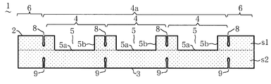
- FIG. 1 is a plan view showing a multi-piece wiring board 1 according to an embodiment of the present invention
- FIG. 2 is a vertical sectional view taken along line XX in FIG. 1
- FIG. FIG. 6 is a partially enlarged cross-sectional view taken along the arrow line YY of FIG.
- the multi-cavity wiring board 1 is formed by stacking upper and lower ceramic layers s ⁇ b> 1 and s ⁇ b> 2 made of alumina (ceramic), for example.
- the front surface 2 and the back surface 3 are common to the multi-cavity wiring substrate 1, the wiring substrate portion 4, and the ear portion 6.
- the wiring board portion 4 has a cavity 5 that is open to the surface 2 and has a bottom surface 5a that is rectangular in plan view and a side surface 5b that has four sides, and the surface 2 that is the periphery of the opening of the cavity 5 includes: A sealing area having a rectangular shape in a plan view and a predetermined width is located, and a sealing conductor layer 7 is formed on the sealing area.
- a pad that is electrically connected to the electronic component to be mounted is formed on the bottom surface 5 a of the cavity 5, and a via conductor is formed in the lower ceramic layer s 2 so as to penetrate the back surface 3 of the wiring board portion 4. Are formed with external connection terminals (both not shown).
- the conductor layer 7 and the pad are made of W or Mo. As shown in FIG.
- the dividing grooves 8 and 9 have a drop shape as a whole in a cross section orthogonal to the longitudinal direction. As illustrated in the dividing groove 8 of FIG. It has an arc-shaped cross section including a semicircle, and has an intermediate portion (opening) 8a between the deepest portion 8b and the groove inlet 8c.
- the width w2 of the deepest part 8b is larger than the width w3 of the groove inlet 8c, and the width w1 of the intermediate part 8a is equal to or smaller than the width w3 of the groove inlet 8c (w2> w3 ⁇ w1).
- the radius R of the deepest part 8b is 6 ⁇ m or more.
- the dividing grooves 8 and 9 face each other in a symmetric posture in the thickness direction of the front surface 2 and the back surface 3 of the multi-piece wiring substrate 1, and the total depth of the dividing grooves 8 and 9 is It is about 60% of the thickness of the front surface 2 and the back surface 3.
- the deepest portion 8 b (depth) of the dividing groove 8 is at a position shallower than the bottom surface 5 a of the cavity 5.
- the multi-piece wiring board 1 as described above, it is formed on the front surface 2 and the back surface 3 along the boundary between the wiring board parts 4 and 4 and the boundary between the wiring board part 4 and the ear part 6, as viewed in plan view.
- the deepest portion 8b has an arcuate cross section, the width w2 of the deepest portion 8b is larger than the width w3 of the groove inlet 8c, and the width w1 of the intermediate portion 8a. Is the same as or smaller than the width w3 of the groove inlet 8c.
- a large number of microcracks are not irregularly formed from the vicinity of the deepest portion having the substantially V-shaped cross section toward the inside.
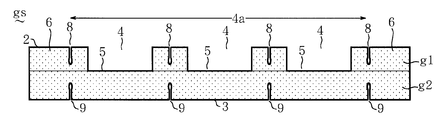
- a ceramic slurry obtained by previously blending alumina powder, a binder resin, a solvent, and the like was formed into a sheet to obtain two green sheets g1 and g2.
- a conductive paste containing W powder is filled in the via hole provided in the green sheet g2 which will be the lower layer later, and the same conductive paste as described above is printed on at least one of the front and back surfaces of the green sheets g1 and g2. Formed.
- a through hole having a rectangular shape in plan view was punched into the upper green sheet g1, and then green sheets g1 and g2 were laminated and pressed to obtain a green sheet laminate gs.
- the green sheet laminate gs was adsorbed under reduced pressure on the surface of a table (not shown) that moved in the vertical and horizontal directions in plan view.
- a laser irradiation head 10 whose axial direction is vertical is disposed so as to be movable up and down.
- symbol 5 in the figure shows a part of said through-hole provided in the green sheet g1 which becomes a cavity later.
- the wiring board The laser beam L was irradiated from the bed 10 between the portions 4 and 4 or along the boundary between the wiring substrate portion 4 and the ear portion 6.
- the laser L is, for example, a YVO 4 laser, and its focal point F is applied near the surface 2 of the green sheet g1.
- the laser L may be a YAG laser, a carbon dioxide laser, an excimer laser, a semiconductor laser, or a ruby laser.
- a small groove d1 having a substantially U-shaped cross section perpendicular to the longitudinal direction was formed along the boundary along the surface 2 of the green sheet g1.
- the laser L was irradiated in the same manner as described above so that the focal point F hits the vicinity of the surface 2 of the green sheet g1 along the small groove d1.
- the laser L was focused at the focal point F near the surface 2 and then spread in a substantially conical shape inside the green sheet g1.
- an intermediate groove d2 is formed along the small groove d1 where the deepest portion d2b is deeper than the small groove d1 and the deepest portion d2b is wider than the opening d2a. It was done.
- the laser L was irradiated in the same manner as described above so that the focal point F hits the vicinity of the surface 2 of the green sheet g1 along the middle groove d2.
- the laser L was also expanded in a substantially conical shape inside the green sheet g1 after being focused at the focal point F near the surface 2.
- the position of the deepest portion 8b is deeper than the deepest portion d2b of the middle groove d2
- the width w2 of the deepest portion 8b is the width of the groove inlet 8c.
- Divided grooves 8 larger than the width w1 of w3 and the intermediate part (opening part) 8a were formed.
- the width w1 of the intermediate portion 8a was the same as or smaller than the width w3 of the groove inlet 8c.
- the dividing groove 8 scans the laser L the same number of times so as to irradiate the green sheet g1 with the laser L at least three times, thereby obtaining the desired depth, the deepest portion 8b and the intermediate portion. It is possible to make the cross-sectional shape and size of 8a.
- a YVO 4 laser of 50 Hz and an output of 5 W is positioned on the same surface 2 while keeping the focal point on the surface 2 of the green sheet g 1 with respect to the green sheet g 1 having a thickness of 400 ⁇ m and a feed rate of 160 mm / sec.
- irradiation was performed while reciprocating 5 times.
- the cross section orthogonal to the longitudinal direction has an arcuate shape and has a deepest portion (8b) having a depth of about 290 ⁇ m, the width (w3) of the groove inlet (8c) is about 30 ⁇ m, and the intermediate portion (8a)
- a dividing groove (8) having a deepest part (8b) having a width (w2) larger than about 20 ⁇ m in width (w1) could be continuously formed along the surface 2 of the green sheet g1.
- FIG. 8 is a plan view of the green sheet laminate gs shown in FIG. 7 and a vertical sectional view taken along the line U-U in FIG. 7 by the step of forming the dividing grooves 8 by the laser L irradiation.
- the longitudinal direction is perpendicular to the boundary between the wiring board portions 4 and 4 and the longitudinal (Y) direction of the boundary between the wiring board portion 4 and the ear portion 6.
- a plurality of divided grooves 8 having a cross section of the deepest portion 8b having an arc shape and having an intermediate portion 8a and a groove inlet 8c are formed in parallel.
- the broken line in FIG. 7 is a virtual scheduled cutting surface (boundary) cf set along each boundary.
- the boundary between the wiring board parts 4 and 4 and the boundary between the wiring board part 4 and the ear part 6 on the surface 2 of the laminate gs are formed by the step of forming the dividing groove 8 by the laser L irradiation similar to the above.
- the cross section of the deepest portion 8b is arc-shaped along the horizontal (X) direction of the plurality of divided grooves 8 having the intermediate portion 8a and the groove inlet 8c. 1) was obtained.
- a plurality of divided grooves 9 having a lattice shape in plan view are formed as divided grooves 8 as shown in FIG. And symmetrically formed.
- the green sheet laminate gs in which the divided grooves 8 and 9 were formed was fired at a predetermined temperature zone.
- a multi-piece wiring board 1 including ceramic layers s1 and s2 obtained by firing green sheets g1 and g2 was obtained.
- the multi-piece wiring board 1 is finally plated with Ni and Au on the surface of the conductor layer 7 or the like through a plating electrode (not shown) separately formed on the side surface of the ear 6 or by electroless plating. A membrane (neither shown) was coated.
- the focal point F is focused on the front surface 2 and the boundary between the wiring board portions 4 and 4 on the front surface 2 and the back surface 3 of the green sheet laminate gs. Since the laser irradiation matched to the vicinity of the back surface 3 was scanned a plurality of times, the laser L was irradiated in a substantially conical (fan-shaped) form on the inner side of the front surface 2 and the back surface 3. As a result, the energy of the laser L was used to grind and polish the irradiated green sheets g1 and g2 at a high temperature.
- the deepest portion 8b (9b) of the divided grooves 8 and 9 to be formed has an arc shape having a substantially semicircular cross section perpendicular to the longitudinal direction.
- the width w2 of the deepest portion 8b (9b) The width w1 of the intermediate portion 8a (9a) is equal to or smaller than the width w3 of the groove inlet 8c (9c), which is larger than the width w3 of (9c).
- the divided grooves 8 and 9 having the width w2 of the deepest portion 8b larger than the width w1 of the groove inlet 8c and the width w1 of the intermediate portion 8a are formed, it is possible to prevent inadvertent re-entry of ceramic or metal powder.
- the dimensional accuracy of the front surface 2 and the back surface 3 for each wiring board portion 4 can be increased, and a seal area having a required width can be easily secured for each front surface 2 of the wiring board portion 4.
- the total depth of the dividing grooves 8 and 9 on the front surface 2 and the back surface 3 is about 60% of the total thickness, and the deepest portions 8b and 9b whose cross sections are arc-shaped approach each other. Therefore, when separated into individual pieces, the wiring boards 4 and 4 could be divided with high dimensional accuracy by the cut surface 12 connecting the two at the shortest distance.
- FIG. 11 is a cross-sectional view showing a multi-piece wiring board 1a of a different form.
- the multi-piece wiring board 1 a has the same dividing groove on the surface 2 along the boundary between the wiring board parts 4 and 4 and the boundary between the wiring board part 4 and the ear part 6. 8 is formed in a lattice shape vertically and horizontally, but along the boundary of the back surface 3, a conventional dividing groove 15 having a substantially V-shaped cross section is formed in a lattice shape vertically and horizontally.
- the dividing groove 15 can be formed by scanning a plurality of times so that the focal position of the laser L is not changed and the position of the focal point is sequentially deepened.
- FIG. 12 is a cross-sectional view showing a multi-piece wiring board 1b of still another form.
- the multi-cavity wiring board 1 b is formed on the surface 2 between the wiring board parts 4 and 4 and along the boundary between the wiring board part 4 and the ear part 6.
- Divided grooves 18 having the same cross-sectional shape and having the deepest portion deeper than the bottom surface of the cavity 5 are formed in a lattice shape vertically and horizontally, but no divided grooves are formed on the back surface 3 side.
- the depth of the dividing groove 18 is about 50% to about 55% of the thickness of the wiring board 1b.
- the ceramic layers s1 and s2 may be low-temperature fired ceramics such as glass-ceramics.
- Cu or Ag is used for the conductors such as the conductor layer 5.
- the shape of the multi-piece wiring board and the wiring board portion in plan view may be a square.
- the multi-piece wiring board may have three or more ceramic layers, and the green sheet laminate may be formed by laminating and pressing three or more green sheets.
- an electrode for electrolytic plating may be formed on the side surface of the groove, and a connection wiring for plating may be formed between the electrode and each wiring board part 4 or between the wiring board parts 4 and 4. .
- the dividing grooves 8, 9, and 18 are formed to such a depth that the plating connection wiring is not exposed.
- the laser irradiation head 10 may be provided with a focus maintaining mechanism or an autofocus means for always fixing the focus F of the laser L to be irradiated near the surface of the green sheet laminate.
- the multi-cavity wiring board of the present invention it is difficult to cause breakage, chipping or cracking from the vicinity of the dividing groove when the individual wiring board is divided or before the division, so that high reliability can be obtained.
Abstract
Description
しかし、前記のようにレーザ光の照射により形成される断面V字形状の分割溝の場合、該分割溝の最深部付近からセラミック基板の内部に向かって多数のマイクロクラックが不規則に発生する。その結果、設定した深さと異なる深さの分割溝となるため、次の焼成工程、あるいはその後のメッキ工程において、分割溝の付近から不規則な破損を生じたり、更に施される分割工程において、分割化した際に個々の配線基板に欠けや割れが生じてしまう、という問題があった。 Laser light is applied to the surface of the ceramic substrate on which the green sheet laminate is formed by laminating and pressing a plurality of green sheets in order to eliminate the deformation of the wiring board area by the blade and the jetty located near the opening end of the dividing groove. There has been proposed a method of manufacturing a dividing ceramic substrate in which a dividing groove having a chamfer in the opening is formed by eliminating the jetty in the vicinity of the opening end by performing irradiation (scanning) twice (for example,) , See Patent Document 1).
However, in the case of the divided grooves having a V-shaped cross section formed by laser light irradiation as described above, a large number of microcracks are irregularly generated from the vicinity of the deepest portion of the divided grooves toward the inside of the ceramic substrate. As a result, because it becomes a division groove with a depth different from the set depth, in the next firing step, or subsequent plating step, irregular breakage from the vicinity of the division groove, or further in the division step to be performed, There was a problem that when divided, each wiring board would be chipped or cracked.
即ち、本発明による第1の多数個取り配線基板は、複数のセラミック層を積層してなり、表面および裏面を有し、平面視で矩形を呈し且つキャビティを有する複数の配線基板部分を縦横に配列した製品領域と、該製品領域の周囲に沿って位置する耳部と、配線基板部分間の境界および配線基板部分と耳部との境界に沿って表面および裏面の少なくとも一方に形成した分割溝と、を備える多数個取り配線基板であって、上記分割溝は、長手方向と直交する断面において、該分割溝の最深部が円弧形で、且つ該最深部と溝入口との間に中間部を有し、前記最深部の幅は、上記溝入口の幅よりも大きく、上記中間部の幅は、溝入口の幅と同じかこれよりも小さい、ことを特徴とする。 In order to solve the above-mentioned problems, the present invention fixes the focal point of the laser beam near the surface of the laminated body when the green sheet laminated body is irradiated with a laser a plurality of times. The idea is to expand the laser beam.
That is, the first multi-cavity wiring board according to the present invention is formed by laminating a plurality of ceramic layers, has a front surface and a back surface, has a rectangular shape in plan view, and has a plurality of wiring board portions having cavities vertically and horizontally. Divided grooves formed on at least one of the front surface and the back surface along the boundary between the wiring substrate portions and the boundary between the wiring substrate portions and the ear portions, the arrayed product regions, the ear portions positioned along the periphery of the product regions The dividing groove has a cross-section perpendicular to the longitudinal direction, the deepest portion of the dividing groove is arc-shaped, and an intermediate portion between the deepest portion and the groove inlet A width of the deepest portion is larger than a width of the groove inlet, and a width of the intermediate portion is equal to or smaller than a width of the groove inlet.
更に、本発明には、前記セラミック層は、アルミナ、ムライト、ガラス-セラミック、あるいは窒化アルミニウムからなる、第3の多数個取り配線基板も含まれる。 The present invention also includes a second multi-piece wiring board in which the arcuate radius of the deepest part in the dividing groove is 6 μm or more.
Furthermore, the present invention includes a third multi-piece wiring board in which the ceramic layer is made of alumina, mullite, glass-ceramic, or aluminum nitride.
また、本発明には、前記分割溝を形成する工程は、前記グリーンシート積層体における表面および裏面ごとに対し、該表面および裏面付近に焦点を合わせたレーザ照射を、前記境界に沿って複数回走査して行われる、第2の多数個取り配線基板の製造方法も含まれる。
更に、本発明には、前記分割溝を形成する工程で用いるレーザは、YAGレーザ、炭酸ガスレーザ、エキシマレーザ、YVO4レーザ、半導体レーザ、あるいはルビーレーザである、第3の多数個取り配線基板の製造方法も含まれる。 On the other hand, according to the first method of manufacturing a multi-cavity wiring board according to the present invention, a plurality of green sheets each having a conductor layer formed on at least one of the front surface and the back surface and having a cavity opened on at least the top surface are laminated. A step of forming a green sheet laminate by pressure bonding, at least one of a front surface and a back surface of the green sheet laminate, a boundary between a plurality of wiring substrate portions arranged vertically and horizontally, and the wiring substrate portion and the ear portion Forming a dividing groove along the boundary of the substrate, and firing the green sheet laminate in which the dividing groove is formed, and the step of forming the dividing groove includes the surface of the green sheet laminate or Laser irradiation focused on the vicinity of the back surface is performed by scanning a plurality of times along the boundary.
Further, in the present invention, the step of forming the dividing groove includes performing laser irradiation focused on the vicinity of the front surface and the back surface for each of the front surface and the back surface of the green sheet laminate a plurality of times along the boundary. A method for manufacturing a second multi-cavity wiring board, which is performed by scanning, is also included.
Further, according to the present invention, the laser used in the step of forming the dividing groove is a YAG laser, a carbon dioxide gas laser, an excimer laser, a YVO 4 laser, a semiconductor laser, or a ruby laser. A manufacturing method is also included.
更に、前記キャビティは、平面視が矩形の底面と四辺の側面とを有している。
また、前記分割溝は、表面および裏面の少なくとも一方におけるセラミックの露出部分、あるいは導体層に沿った開口部を有している。
更に、分割溝の深さは、前記多数個取り配線基板の厚みの60%以下である。
また、前記分割溝は、前記多数個取り配線基板の表面あるいは裏面のみに形成し、他方の面には何らの分割溝を形成しない形態や、他方の面には従来同様の断面ほぼV字形状の分割溝を形成した形態としても良い。
更に、前記分割溝の最深部は、該分割溝の長手方向と直交する断面において、次述する半径を含む半円形ないし円形の円弧形を呈する。
また、前記分割溝の溝入口は、前記表面に露出する該分割溝のうち、両側の平坦な一対の表面に挟まれた部分を指す。
加えて、前記分割溝の中間部は、当該分割溝の深さが前記キャビティの底面と同じか該底面よりも浅い場合には、前記溝入口と最深部との間の部分を指し、当該分割溝の深さが前記キャビティの底面よりも深い場合には、上記最深部と溝入口との間の部分で且つ上記キャビティの底面よりも深い部分も含む。 The wiring board portion has a cavity open to the front surface and a seal area for attaching a lid for sealing the cavity to the front surface surrounding the cavity, and external connection terminals such as pads formed on the back surface; An internal wiring layer positioned inside the wiring board portion, and further may include a connecting wiring for plating disposed between adjacent wiring board portions or ears.
Further, the cavity has a rectangular bottom surface and four side surfaces in plan view.
The dividing groove has an exposed portion of the ceramic on at least one of the front surface and the back surface, or an opening along the conductor layer.
Further, the depth of the dividing groove is 60% or less of the thickness of the multi-piece wiring board.
In addition, the dividing groove is formed only on the front surface or the back surface of the multi-cavity wiring board, and no dividing groove is formed on the other surface, or the other surface has a substantially V-shaped cross section similar to the conventional one. It is also possible to form such a divided groove.
Further, the deepest portion of the dividing groove has a semicircular or circular arc shape including a radius described below in a cross section perpendicular to the longitudinal direction of the dividing groove.
In addition, the groove entrance of the dividing groove refers to a portion sandwiched between a pair of flat surfaces on both sides of the dividing groove exposed on the surface.
In addition, the middle portion of the dividing groove refers to a portion between the groove entrance and the deepest portion when the depth of the dividing groove is the same as or shallower than the bottom surface of the cavity. When the depth of the groove is deeper than the bottom surface of the cavity, a portion between the deepest portion and the groove entrance and a portion deeper than the bottom surface of the cavity is also included.
しかも、溝入口や中間部(開口部)の幅よりも最深部の幅が大きな分割溝が形成されるため、セラミックや金属粉などの不用意な進入を防止でき、且つ配線基板部分ごとの表面および裏面の寸法精度を高めることにも寄与し得る。 On the other hand, according to the first manufacturing method, laser irradiation is performed a plurality of times along the boundary between the front and back surfaces of the green sheet laminate, such as between the wiring substrate portions, with the focal point being in the vicinity of the front or back surface. The laser beam is irradiated in a substantially fan-shaped manner on the inner side of the front and back surfaces. Since the energy of the laser grinds and polishes the inside of the irradiated green sheet at a high temperature, the deepest part of the formed dividing groove has an arc shape having a substantially semicircular cross section perpendicular to the longitudinal direction. As a result, it is possible to prevent or suppress a situation in which a large number of microcracks are irregularly generated from the narrowest deepest portion to the inside, as in a conventional dividing groove having a substantially V-shaped cross section. Therefore, it is possible to eliminate or suppress inadvertent cracking and chipping in the subsequent firing process and the like.
Moreover, since the dividing groove having the deepest portion wider than the width of the groove entrance and the intermediate portion (opening) is formed, it is possible to prevent inadvertent entry of ceramics or metal powder, and the surface of each wiring board portion. It can also contribute to increasing the dimensional accuracy of the back surface.
尚、前記グリーンシート積層体は、表面と裏面との少なくとも一方に配線層などの導体層が形成された2層以上のグリーンシートを積層し圧着したものである。
また、前記グリーンシート積層体における配線基板部分同士間の境界、および配線基板部分と耳部との境界には、予め仮想の切断予定面が設定されている。
更に、前記グリーンシート積層体は、矩形の金属枠の内側に張り付けられ、該金属枠と共に、例えば、移動可能なテーブルの表面に減圧吸着により固定される。
また、分割溝の全深さは、グリーンシート積層体の厚みの60%以下である。
尚、前記グリーンシート積層体の同じ表面あるいは裏面の同じ位置に対し、前記レーザ照射を走査する回数は、レーザの条件などによって相違するが、グリーンシートに一般的な深さの分割溝を形成するには、少なくとも2回、望ましくは3回~7回程度にわたり連続的に照射することが望ましい。 Further, according to the second manufacturing method, since the laser irradiation focused on the front surface and the back surface of the green sheet laminate is scanned a plurality of times, the deepest section has an arc shape and the deepest section Dividing grooves having a width larger than the width of the groove inlet and the width of the intermediate portion (opening) can be formed symmetrically and opposed to the front surface and the back surface.
The green sheet laminate is formed by laminating and pressing two or more green sheets in which a conductor layer such as a wiring layer is formed on at least one of the front surface and the back surface.
In addition, virtual cutting planes are set in advance at the boundary between the wiring board parts in the green sheet laminate and the boundary between the wiring board part and the ear part.
Further, the green sheet laminate is attached to the inside of a rectangular metal frame, and is fixed together with the metal frame, for example, on the surface of a movable table by vacuum suction.
Further, the total depth of the dividing grooves is 60% or less of the thickness of the green sheet laminate.
The number of times the laser irradiation is scanned with respect to the same position on the front surface or the back surface of the green sheet laminate is different depending on the laser conditions, but a division groove having a general depth is formed in the green sheet. In this case, it is desirable to continuously irradiate at least twice, preferably about 3 to 7 times.
図1は、本発明による一形態の多数個取り配線基板1を示す平面図、図2は、図1中のX-X線の矢視に沿った垂直断面図、図3は、図1中のY-Y線の矢視に沿った部分拡大断面図および同図中の一点鎖線部分Zの部分拡大図である。
多数個取り配線基板1は、図1,図2に示すように、例えば、アルミナ(セラミック)からなる上下2層(複数)のセラミック層s1,s2を積層してなり、平面視が長方形(矩形)の表面(主面)2および裏面(主面)3を有し、平面視が長方形(矩形)を呈する複数の配線基板部分4を縦横に配列した製品領域4aと、該製品領域4aの周囲に沿って位置する矩形枠状の耳部6と、隣接する配線基板部分4,4間の境界および配線基板部分4と耳部6との境界に沿って表面2および裏面3に対称に形成された分割溝8,9とを備えている。
尚、前記表面2および裏面3は、前記多数個取り配線基板1、配線基板部分4、および耳部6に共通している。 Hereinafter, modes for carrying out the present invention will be described.
FIG. 1 is a plan view showing a multi-piece wiring board 1 according to an embodiment of the present invention, FIG. 2 is a vertical sectional view taken along line XX in FIG. 1, and FIG. FIG. 6 is a partially enlarged cross-sectional view taken along the arrow line YY of FIG.
As shown in FIGS. 1 and 2, the multi-cavity wiring board 1 is formed by stacking upper and lower ceramic layers s <b> 1 and s <b> 2 made of alumina (ceramic), for example. A
The
図2に示すように、分割溝8,9は、長手方向と直交する断面において、全体が滴(しずく)形状を呈し、図3の分割溝8で例示するように、最深部8bが、ほぼ半円形を含む円弧形の断面で、該最深部8bと溝入口8cとの間に中間部(開口部)8aを有している。上記最深部8bの幅w2は、溝入口8cの幅w3よりも大きく、中間部8aの幅w1は、溝入口8cの幅w3と同じかこれよりも小さい(w2>w3≧w1)。上記最深部8bの半径Rは、6μm以上である。該最深部8bの断面ほぼ半円形を呈する内壁面には、内部に進入するマイクロクラックがないか、あるいは極く僅かで且つ短いマイクロクラックしか形成されていない。その原因は、後述するレーザ照射による分割溝形成工程に起因している。 The
As shown in FIG. 2, the dividing
以上のような多数個取り配線基板1によれば、前記配線基板部分4,4間の境界および配線基板部分4と耳部6との境界に沿って表面2および裏面3に形成され、平面視が格子形状を呈する分割溝8,9は、それらの最深部8bの断面が円弧形で、該最深部8bの幅w2が、溝入口8cの幅w3よりも大きく、中間部8aの幅w1が溝入口8cの幅w3と同じかこれよりも小さい。これにより、従来の分割溝のように、断面がほぼV字形状で最も狭い最深部付近から内部に向かって多数のマイクロクラックが不規則に形成されていない。
そのため、製造時の焼成工程やメッキ工程、更には分割時において、分割溝8,9付近からの不用意な破損や欠けや割れが生じにくく、所定の位置において容易に切断できる。しかも、溝入口8cの幅w3が最深部8bの幅w2よりも小さいため、配線基板部分4ごとのキャビティ5を囲む表面2に位置するシールエリアの幅を大きくできるので、該エリア上に封止性の高い導体層7を容易に形成することができる。従って、形状および寸法精度に優れ、高い信頼性を有している。 As shown in FIG. 2, the dividing
According to the multi-piece wiring board 1 as described above, it is formed on the
Therefore, in the firing process and plating process at the time of manufacturing, and further at the time of division, inadvertent breakage, chipping and cracking from the vicinity of the
予め、アルミナ粉末、バインダ樹脂、および溶剤などを配合して得られたセラミックスラリをシート化して、2枚のグリーンシートg1,g2を得た。このうち、追って下層側となるグリーンシートg2に設けたビアホールにW粉末を含む導電性ペーストを充填し、且つグリーンシートg1,g2の表面および裏面の少なくとも一方に上記同様の導電性ペーストを印刷にて形成した。次に、上層側となるグリーンシートg1に平面視が長方形の貫通孔を打ち抜き加工した後、グリーンシートg1,g2を積層および圧着してグリーンシート積層体gsを得た。
次いで、上記グリーンシート積層体gsを平面視で縦横方向に移動するテーブル(図示せず)の表面に減圧吸着した。該テーブルの上方には、図4の左側に示すように、軸方向が垂直であるレーザ照射ヘッド10が昇降可能に配置してある。尚、同図中の符号5は、追ってキャビティとなるグリーンシートg1に設けた上記貫通孔の一部を示す。 Hereinafter, a method for manufacturing the multi-piece wiring board 1 will be described.
A ceramic slurry obtained by previously blending alumina powder, a binder resin, a solvent, and the like was formed into a sheet to obtain two green sheets g1 and g2. Among these, a conductive paste containing W powder is filled in the via hole provided in the green sheet g2 which will be the lower layer later, and the same conductive paste as described above is printed on at least one of the front and back surfaces of the green sheets g1 and g2. Formed. Next, a through hole having a rectangular shape in plan view was punched into the upper green sheet g1, and then green sheets g1 and g2 were laminated and pressed to obtain a green sheet laminate gs.
Next, the green sheet laminate gs was adsorbed under reduced pressure on the surface of a table (not shown) that moved in the vertical and horizontal directions in plan view. Above the table, as shown on the left side of FIG. 4, a
その結果、図4の右側に示すように、グリーンシートg1の表面2に沿って長手方向と直交する断面がほぼU字形の小溝d1が前記境界に沿って形成された。
次いで、図5の左側に示すように、上記小溝d1に沿って、焦点Fをグリーンシートg1の表面2付近に当たるようにして、前記レーザLを前記同様に照射した。同図中の二点鎖線で示すように、該レーザLは、表面2付近の焦点Fで絞られた後、グリーンシートg1の内部では、ほぼ円錐形状に拡がっていた。その結果、図5の右側に示すように、最深部d2bの位置が小溝d1よりも深く、且つ該最深部d2bの幅が開口部d2aの幅よりも大きな中溝d2が前記小溝d1に沿って形成された。 In this state, by moving the green sheet laminate gs together with the table in the horizontal direction, as shown on the left side of FIG. 4, on the
As a result, as shown on the right side of FIG. 4, a small groove d1 having a substantially U-shaped cross section perpendicular to the longitudinal direction was formed along the boundary along the
Next, as shown on the left side of FIG. 5, the laser L was irradiated in the same manner as described above so that the focal point F hits the vicinity of the
尚、上記分割溝8は、グリーンシートg1に対して、前記レーザLを少なくとも3回以上照射するように、該レーザLを同じ回数走査することにより、所望の深さと、最深部8bおよび中間部8aの断面形状と寸法にすることが可能である。 Further, as shown on the left side of FIG. 6, the laser L was irradiated in the same manner as described above so that the focal point F hits the vicinity of the
The dividing
その結果、長手方向と直交する断面が円弧形で且つ深さが約290μmの最深部(8b)を有し、溝入口(8c)の幅(w3)約30μm、および中間部(8a)の幅(w1)約20μmよりも大きい幅(w2)の最深部(8b)を有する分割溝(8)を、上記グリーンシートg1の表面2に沿って連続して形成することができた。
前記レーザLの照射による分割溝8を形成する工程によって、図7に示すグリーンシート積層体gsの平面図、および該図7中のU-U線の矢視に沿った垂直断面図の図8で示すように、上記積層体gsの表面2において、配線基板部分4,4間の境界、および配線基板部分4と耳部6との境界の縦(Y)方向に沿って、長手方向と直交し、最深部8bの断面が円弧形で且つ中間部8aや溝入口8cを有する複数の分割溝8が平行に形成された。尚、図7中の破線は、上記境界ごとに沿って設定された仮想の切断予定面(境界)cfである。 Incidentally, a YVO 4 laser of 50 Hz and an output of 5 W is positioned on the
As a result, the cross section orthogonal to the longitudinal direction has an arcuate shape and has a deepest portion (8b) having a depth of about 290 μm, the width (w3) of the groove inlet (8c) is about 30 μm, and the intermediate portion (8a) A dividing groove (8) having a deepest part (8b) having a width (w2) larger than about 20 μm in width (w1) could be continuously formed along the
FIG. 8 is a plan view of the green sheet laminate gs shown in FIG. 7 and a vertical sectional view taken along the line U-U in FIG. 7 by the step of forming the dividing
更に、グリーンシート積層体gsの裏面3においても、前記同様のレーザLを照射する工程を施すことにより、図9に示すように、平面視が格子形を呈する複数の分割溝9が分割溝8と対称に形成された。
次いで、分割溝8,9が形成された前記グリーンシート積層体gsを所定の温度帯で焼成した。その結果、前記図1,図2に示したように、グリーンシートg1,g2が焼成されたセラミック層s1,s2を含む多数個取り配線基板1が得られた。そして、該多数個取り配線基板1は、最後に、耳部6の側面に別途形成した図示しないメッキ用電極を介して、あるいは無電解メッキにより、前記導体層7などの表面にNiおよびAuメッキ膜(何れも図示せず)を被覆された。 Subsequently, the boundary between the wiring
Furthermore, also on the
Next, the green sheet laminate gs in which the divided
しかも、図10に示すように、表面2,裏面3の分割溝8,9の全深さは、全体の厚みの約60%であり、断面が円弧形の最深部8b,9bが接近しているので、個片化した際には、両者を最短距離で結ぶ切断面12で配線基板4,4を、寸法精度良く分割することができた。 Furthermore, since the divided
Moreover, as shown in FIG. 10, the total depth of the dividing
多数個取り配線基板1aは、図11に示すように、表面2には、前記配線基板部分4,4間、および配線基板部分4と耳部6との境界に沿って、前記同様の分割溝8が縦横に格子状に形成されているが、裏面3の上記境界に沿っては、従来の断面ほぼV字形の分割溝15が縦横に格子状に形成されている。尚、かかる分割溝15は、前記レーザLの焦点Fの距離を変えず、該焦点の位置を順次深くするように、複数回走査することで形成することもできる。
かかる多数個取り配線基板1aによっても、表面2側に形成した前記同様の分割溝8の最深部8bには、前述したようにマイクロクラックの発生が抑制されているため、焼成工程以降や分割工程において、不用意な割れや欠けを低減することが可能である。 FIG. 11 is a cross-sectional view showing a multi-piece wiring board 1a of a different form.
As shown in FIG. 11, the multi-piece wiring board 1 a has the same dividing groove on the
Even in the multi-cavity wiring board 1a, since the occurrence of microcracks is suppressed in the
多数個取り配線基板1bは、図12に示すように、表面2には、前記配線基板部分4,4間、および配線基板部分4と耳部6との境界に沿って、前記分割溝8と同様の断面形状を有し且つ最深部がキャビティ5の底面よりも深い分割溝18が縦横に格子状に形成されているが、裏面3側には、分割溝は形成されていない。上記分割溝18の深さは、上記配線基板1bの厚みの約50%~約55%である。かかる多数個取り配線基板1bによっても、表面2側のみに形成した比較的深い分割溝18には、前述したようにマイクロクラックの発生が抑制されているため、焼成工程以降や分割工程において、不用意な割れや欠けを抑制することが可能である。更に、分割溝18の最深部がキャビティ5の底面よりも深い位置にあるため、キャビティ5を囲む四辺の側壁の厚みが比較的均一で且つ強固となる。 FIG. 12 is a cross-sectional view showing a
As shown in FIG. 12, the
例えば、前記セラミック層s1,s2は、ガラス-セラミックのような低温焼成セラミックであっても良く、この際、前記導体層5などの導体には、CuやAgが用いられる。
また、前記多数個取り配線基板や配線基板部分の平面視の形状は、正方形であっても良い。
更に、前記多数個取り配線基板は、3層以上のセラミック層を有していても良く、且つ前記グリーンシート積層体も、3層以上のグリーンシートを積層し且つ圧着していても良い。
また、前記溝の側面には、電解メッキ用の電極が形成され、該電極と各配線基板部分4との間や配線基板部分4,4間にメッキ用接続配線が形成された形態としても良い。この形態では、前記分割溝8,9,18は、上記メッキ用接続配線が露出しない深さで形成される。
加えて、前記レーザ照射ヘッド10は、照射するレーザLの焦点Fを常にグリーンシート積層体の表面付近に固定するための焦点維持機構、あるいはオートフォーカス手段を備えていても良い。 The present invention is not limited to the embodiment described above.
For example, the ceramic layers s1 and s2 may be low-temperature fired ceramics such as glass-ceramics. In this case, Cu or Ag is used for the conductors such as the
Moreover, the shape of the multi-piece wiring board and the wiring board portion in plan view may be a square.
Further, the multi-piece wiring board may have three or more ceramic layers, and the green sheet laminate may be formed by laminating and pressing three or more green sheets.
In addition, an electrode for electrolytic plating may be formed on the side surface of the groove, and a connection wiring for plating may be formed between the electrode and each
In addition, the
2…………………表面
3…………………裏面
4…………………配線基板部分
4a………………製品領域
5…………………キャビティ
6…………………耳部
7…………………導体層
8,9,18……分割溝
8a………………中間部
8b………………最深部
8c………………溝入口
g1,g2………グリーンシート
gs………………グリーンシート積層体
s1,s2………セラミック層
L…………………レーザ
F…………………焦点
w1,w2………幅
R…………………半径
cf………………切断予定面(境界) 1, 1a, 1b ...
Claims (6)
- 複数のセラミック層を積層してなり、表面および裏面を有し、平面視で矩形を呈し且つキャビティを有する複数の配線基板部分を縦横に配列した製品領域と、該製品領域の周囲に沿って位置する耳部と、配線基板部分間の境界および配線基板部分と耳部との境界に沿って表面および裏面の少なくとも一方に形成した分割溝と、を備える多数個取り配線基板であって、
上記分割溝は、長手方向と直交する断面において、該分割溝の最深部が円弧形で、且つ該最深部と溝入口との間に中間部を有し、
上記最深部の幅は、上記溝入口の幅よりも大きく、上記中間部の幅は、溝入口の幅と同じかこれよりも小さい、
ことを特徴とする多数個取り配線基板。 A product region formed by laminating a plurality of ceramic layers, having a front surface and a back surface , a rectangular shape in plan view , and a plurality of wiring board portions having cavities arranged vertically and horizontally, and positioned along the periphery of the product region A multi-piece wiring board comprising: an ear part to be formed; and a dividing groove formed on at least one of the front surface and the back surface along the boundary between the wiring board part and the boundary between the wiring board part and the ear part,
In the cross section perpendicular to the longitudinal direction, the dividing groove has an arcuate deepest part of the dividing groove, and an intermediate part between the deepest part and the groove inlet,
The width of the deepest part is larger than the width of the groove inlet, and the width of the intermediate part is the same as or smaller than the width of the groove inlet.
A multi-piece wiring board characterized by that. - 前記分割溝における最深部の円弧形の半径は、6μm以上である、
ことを特徴とする請求項1に記載の多数個取り配線基板。 The arcuate radius of the deepest part in the dividing groove is 6 μm or more.
The multi-piece wiring board according to claim 1, wherein: - 前記セラミック層は、アルミナ、ムライト、ガラス-セラミック、あるいは窒化アルミニウムからなる、
ことを特徴とする請求項1または2に記載の多数個取り配線基板。 The ceramic layer is made of alumina, mullite, glass-ceramic, or aluminum nitride.
The multi-piece wiring board according to claim 1, wherein the multi-piece wiring board is provided. - 表面および裏面の少なくとも一方に導体層が形成され且つ少なくとも最上層の表面に開口するキャビティが形成された複数のグリーンシートを積層および圧着してグリーンシート積層体を形成する工程と、
上記グリーンシート積層体における表面および裏面の少なくとも一方において、縦横に配列された複数の配線基板部分間の境界および該配線基板部分と耳部との境界に沿って分割溝を形成する工程と、
上記分割溝が形成されたグリーンシート積層体を焼成する工程と、を備え、
上記分割溝を形成する工程は、グリーンシート積層体の上記表面または裏面付近に焦点を合わせたレーザ照射を、上記境界に沿って複数回走査することで行われる、
ことを特徴とする多数個取り配線基板の製造方法。 A step of laminating and pressing a plurality of green sheets each having a conductor layer formed on at least one of the front surface and the back surface and having a cavity formed at least on the surface of the uppermost layer to form a green sheet laminate;
Forming at least one of the front surface and the back surface of the green sheet laminate, a dividing groove along a boundary between a plurality of wiring substrate portions arranged vertically and horizontally, and a boundary between the wiring substrate portion and the ear portion; and
Firing the green sheet laminate in which the divided grooves are formed,
The step of forming the dividing groove is performed by scanning the laser irradiation focused on the front surface or the back surface of the green sheet laminated body a plurality of times along the boundary.
A method of manufacturing a multi-cavity wiring board characterized by the above. - 前記分割溝を形成する工程は、前記グリーンシート積層体における表面および裏面ごとに対し、該表面および裏面付近に焦点を合わせたレーザ照射を、前記境界に沿って複数回走査して行われる、
ことを特徴とする請求項4に記載の多数個取り配線基板の製造方法。 The step of forming the division grooves is performed by scanning the laser irradiation focused on the vicinity of the front surface and the back surface a plurality of times along the boundary with respect to the front surface and the back surface of the green sheet laminate.
The method for manufacturing a multi-piece wiring board according to claim 4. - 前記分割溝を形成する工程で用いるレーザは、YAGレーザ、炭酸ガスレーザ、エキシマレーザ、YVO4レーザ、半導体レーザ、あるいはルビーレーザである、
ことを特徴とする請求項4または5に記載の多数個取り配線基板の製造方法。 The laser used in the step of forming the dividing groove is a YAG laser, a carbon dioxide gas laser, an excimer laser, a YVO 4 laser, a semiconductor laser, or a ruby laser.
The method for manufacturing a multi-piece wiring board according to claim 4 or 5, wherein:
Priority Applications (5)
| Application Number | Priority Date | Filing Date | Title |
|---|---|---|---|
| KR1020137007369A KR101432952B1 (en) | 2010-10-08 | 2011-09-30 | Multi-cavity wiring board and method for manufacturing same |
| EP11830572.1A EP2627159A4 (en) | 2010-10-08 | 2011-09-30 | Multi-cavity wiring board and method for manufacturing same |
| JP2012501475A JP5665145B2 (en) | 2010-10-08 | 2011-09-30 | Multi-piece wiring board and manufacturing method thereof |
| CN201180046378.XA CN103120034B (en) | 2010-10-08 | 2011-09-30 | Many circuit board and manufacture methods thereof in flakes |
| US13/876,670 US9049793B2 (en) | 2010-10-08 | 2011-09-30 | Multi-piece-array and method of manufacturing the same |
Applications Claiming Priority (2)
| Application Number | Priority Date | Filing Date | Title |
|---|---|---|---|
| JP2010-228039 | 2010-10-08 | ||
| JP2010228039 | 2010-10-08 |
Publications (1)
| Publication Number | Publication Date |
|---|---|
| WO2012046640A1 true WO2012046640A1 (en) | 2012-04-12 |
Family
ID=45927635
Family Applications (1)
| Application Number | Title | Priority Date | Filing Date |
|---|---|---|---|
| PCT/JP2011/072510 WO2012046640A1 (en) | 2010-10-08 | 2011-09-30 | Multi-cavity wiring board and method for manufacturing same |
Country Status (7)
| Country | Link |
|---|---|
| US (1) | US9049793B2 (en) |
| EP (1) | EP2627159A4 (en) |
| JP (1) | JP5665145B2 (en) |
| KR (1) | KR101432952B1 (en) |
| CN (1) | CN103120034B (en) |
| TW (1) | TWI449473B (en) |
| WO (1) | WO2012046640A1 (en) |
Cited By (2)
| Publication number | Priority date | Publication date | Assignee | Title |
|---|---|---|---|---|
| JP2014083798A (en) * | 2012-10-25 | 2014-05-12 | Mitsuboshi Diamond Industrial Co Ltd | Method of segmenting laminated ceramic substrate |
| WO2021200878A1 (en) * | 2020-03-30 | 2021-10-07 | デンカ株式会社 | Aluminum nitride plate and method for producing same, composite substrate and method for producing same, and circuit board and method for producing same |
Families Citing this family (9)
| Publication number | Priority date | Publication date | Assignee | Title |
|---|---|---|---|---|
| JP6006474B2 (en) * | 2011-04-25 | 2016-10-12 | 日本特殊陶業株式会社 | Wiring board, multi-cavity wiring board, and manufacturing method thereof |
| US9491867B2 (en) * | 2014-09-30 | 2016-11-08 | Ngk Spark Plug Co., Ltd. | Wiring substrate and multi-piece wiring substrate |
| JP2016072606A (en) * | 2014-09-30 | 2016-05-09 | 日本特殊陶業株式会社 | Wiring board and multi-piece wiring board |
| KR102281459B1 (en) * | 2014-11-05 | 2021-07-27 | 삼성전기주식회사 | Printed circuit board and manufacturing method thereof |
| CN108781502B (en) | 2016-04-22 | 2021-11-30 | 京瓷株式会社 | Multi-piece wiring board and wiring board |
| JP6724775B2 (en) * | 2016-12-28 | 2020-07-15 | 凸版印刷株式会社 | Wiring board individualization method and package board |
| JP6943617B2 (en) * | 2017-05-16 | 2021-10-06 | 住友電気工業株式会社 | Substrate for printed wiring board and manufacturing method of printed wiring board |
| JP6550516B1 (en) * | 2018-09-18 | 2019-07-24 | レノボ・シンガポール・プライベート・リミテッド | Panel, PCB and PCB manufacturing method |
| CN109585162B (en) * | 2018-12-29 | 2020-11-17 | 广东芯晟电子科技有限公司 | Low-stress single-layer chip capacitor and preparation method thereof |
Citations (4)
| Publication number | Priority date | Publication date | Assignee | Title |
|---|---|---|---|---|
| JP2004276386A (en) * | 2003-03-14 | 2004-10-07 | Koa Corp | Splitting ceramic substrate and its manufacturing method |
| JP2007165540A (en) * | 2005-12-13 | 2007-06-28 | Tdk Corp | Method for manufacturing multilayer ceramic substrate, and the multilayer ceramic aggregate substrate |
| JP2009033023A (en) * | 2007-07-30 | 2009-02-12 | Ngk Spark Plug Co Ltd | Method of manufacturing multi-piece substrate |
| JP2010225910A (en) * | 2009-03-24 | 2010-10-07 | Ngk Spark Plug Co Ltd | Multiple patterning ceramic wiring board |
Family Cites Families (2)
| Publication number | Priority date | Publication date | Assignee | Title |
|---|---|---|---|---|
| JPS62232187A (en) | 1986-04-02 | 1987-10-12 | 松下電器産業株式会社 | Manufacture of ceramic circuit board |
| JP4602738B2 (en) * | 2004-10-29 | 2010-12-22 | 太陽社電気株式会社 | Manufacturing method of chip resistor |
-
2011
- 2011-09-30 EP EP11830572.1A patent/EP2627159A4/en not_active Withdrawn
- 2011-09-30 KR KR1020137007369A patent/KR101432952B1/en not_active IP Right Cessation
- 2011-09-30 JP JP2012501475A patent/JP5665145B2/en not_active Expired - Fee Related
- 2011-09-30 US US13/876,670 patent/US9049793B2/en not_active Expired - Fee Related
- 2011-09-30 CN CN201180046378.XA patent/CN103120034B/en not_active Expired - Fee Related
- 2011-09-30 WO PCT/JP2011/072510 patent/WO2012046640A1/en active Application Filing
- 2011-10-06 TW TW100136187A patent/TWI449473B/en not_active IP Right Cessation
Patent Citations (4)
| Publication number | Priority date | Publication date | Assignee | Title |
|---|---|---|---|---|
| JP2004276386A (en) * | 2003-03-14 | 2004-10-07 | Koa Corp | Splitting ceramic substrate and its manufacturing method |
| JP2007165540A (en) * | 2005-12-13 | 2007-06-28 | Tdk Corp | Method for manufacturing multilayer ceramic substrate, and the multilayer ceramic aggregate substrate |
| JP2009033023A (en) * | 2007-07-30 | 2009-02-12 | Ngk Spark Plug Co Ltd | Method of manufacturing multi-piece substrate |
| JP2010225910A (en) * | 2009-03-24 | 2010-10-07 | Ngk Spark Plug Co Ltd | Multiple patterning ceramic wiring board |
Non-Patent Citations (1)
| Title |
|---|
| See also references of EP2627159A4 * |
Cited By (2)
| Publication number | Priority date | Publication date | Assignee | Title |
|---|---|---|---|---|
| JP2014083798A (en) * | 2012-10-25 | 2014-05-12 | Mitsuboshi Diamond Industrial Co Ltd | Method of segmenting laminated ceramic substrate |
| WO2021200878A1 (en) * | 2020-03-30 | 2021-10-07 | デンカ株式会社 | Aluminum nitride plate and method for producing same, composite substrate and method for producing same, and circuit board and method for producing same |
Also Published As
| Publication number | Publication date |
|---|---|
| JP5665145B2 (en) | 2015-02-04 |
| KR101432952B1 (en) | 2014-08-21 |
| TWI449473B (en) | 2014-08-11 |
| JPWO2012046640A1 (en) | 2014-02-24 |
| US9049793B2 (en) | 2015-06-02 |
| KR20130048788A (en) | 2013-05-10 |
| TW201223346A (en) | 2012-06-01 |
| CN103120034B (en) | 2016-08-03 |
| EP2627159A4 (en) | 2018-01-17 |
| CN103120034A (en) | 2013-05-22 |
| US20130183475A1 (en) | 2013-07-18 |
| EP2627159A1 (en) | 2013-08-14 |
Similar Documents
| Publication | Publication Date | Title |
|---|---|---|
| JP5665145B2 (en) | Multi-piece wiring board and manufacturing method thereof | |
| TWI488548B (en) | Ceramic wiring substrate, multi-piece ceramic wiring substrate and method for manufacturing the same | |
| EP3349244A1 (en) | Electronic component storage package, multi-piece wiring substrate, electronic device, and electronic module | |
| TWI488551B (en) | Wiring substrate, multi-piece wiring substrate and method for manufacturing the same | |
| TWI495403B (en) | Wiring substrate, multi-piece wiring substrate and method for manufacturing the same | |
| JP6930573B2 (en) | Silicon nitride based ceramic assembly substrate | |
| JP2009252971A (en) | Metal-ceramics bonding substrate, manufacturing method therefor, and metal-ceramics bonding body | |
| JP5448400B2 (en) | Manufacturing method of ceramic parts | |
| JP6587205B2 (en) | Silicon nitride ceramic aggregate substrate and method for manufacturing the same, and method for manufacturing silicon nitride ceramic sintered substrate | |
| JP4929893B2 (en) | Manufacturing method of ceramic substrate | |
| JP6317115B2 (en) | Multi-cavity wiring board, wiring board, and manufacturing method of multi-cavity wiring board | |
| TWI488550B (en) | Wiring substrate, multi-piece wiring substrate and method for manufacturing the same | |
| JP5574804B2 (en) | Multiple wiring board | |
| JP2018046266A (en) | Multi-piece wiring board and manufacturing method for multi-piece wiring board | |
| JP6029173B2 (en) | Ceramic package and manufacturing method thereof | |
| JP2006128363A (en) | Multiple patterning wiring board and electronic device | |
| JP2005072210A (en) | Laminated board, package, and method of manufacturing them | |
| JP2019047005A (en) | Multi-cavity ceramic substrate and manufacturing method thereof | |
| JP5946249B2 (en) | Manufacturing method of multi-cavity wiring board | |
| JP2016149419A (en) | Multi-piece wiring board manufacturing method | |
| JP2013122979A (en) | Multiple patterning wiring board and method for manufacturing the same | |
| JP2012256731A (en) | Multi-piece wiring board and method of manufacturing the same | |
| JP2015103612A (en) | Substrate for electronic element housing member, method of manufacturing electronic element housing member, electronic element housing package, and electronic device | |
| JP2006066680A (en) | Package |
Legal Events
| Date | Code | Title | Description |
|---|---|---|---|
| WWE | Wipo information: entry into national phase |
Ref document number: 201180046378.X Country of ref document: CN |
|
| WWE | Wipo information: entry into national phase |
Ref document number: 2012501475 Country of ref document: JP |
|
| 121 | Ep: the epo has been informed by wipo that ep was designated in this application |
Ref document number: 11830572 Country of ref document: EP Kind code of ref document: A1 |
|
| ENP | Entry into the national phase |
Ref document number: 20137007369 Country of ref document: KR Kind code of ref document: A |
|
| WWE | Wipo information: entry into national phase |
Ref document number: 2011830572 Country of ref document: EP |
|
| WWE | Wipo information: entry into national phase |
Ref document number: 13876670 Country of ref document: US |
|
| NENP | Non-entry into the national phase |
Ref country code: DE |