WO2012046602A1 - 故障検出システム、取出装置、故障検出方法、プログラム及び記録媒体 - Google Patents
故障検出システム、取出装置、故障検出方法、プログラム及び記録媒体 Download PDFInfo
- Publication number
- WO2012046602A1 WO2012046602A1 PCT/JP2011/072211 JP2011072211W WO2012046602A1 WO 2012046602 A1 WO2012046602 A1 WO 2012046602A1 JP 2011072211 W JP2011072211 W JP 2011072211W WO 2012046602 A1 WO2012046602 A1 WO 2012046602A1
- Authority
- WO
- WIPO (PCT)
- Prior art keywords
- output
- logic
- values
- holding
- failure
- Prior art date
- Legal status (The legal status is an assumption and is not a legal conclusion. Google has not performed a legal analysis and makes no representation as to the accuracy of the status listed.)
- Ceased
Links
Images








Classifications
-
- G—PHYSICS
- G01—MEASURING; TESTING
- G01R—MEASURING ELECTRIC VARIABLES; MEASURING MAGNETIC VARIABLES
- G01R31/00—Arrangements for testing electric properties; Arrangements for locating electric faults; Arrangements for electrical testing characterised by what is being tested not provided for elsewhere
- G01R31/28—Testing of electronic circuits, e.g. by signal tracer
- G01R31/317—Testing of digital circuits
- G01R31/3177—Testing of logic operation, e.g. by logic analysers
-
- G—PHYSICS
- G01—MEASURING; TESTING
- G01R—MEASURING ELECTRIC VARIABLES; MEASURING MAGNETIC VARIABLES
- G01R31/00—Arrangements for testing electric properties; Arrangements for locating electric faults; Arrangements for electrical testing characterised by what is being tested not provided for elsewhere
- G01R31/28—Testing of electronic circuits, e.g. by signal tracer
- G01R31/317—Testing of digital circuits
- G01R31/3181—Functional testing
- G01R31/3183—Generation of test inputs, e.g. test vectors, patterns or sequences
-
- G—PHYSICS
- G01—MEASURING; TESTING
- G01R—MEASURING ELECTRIC VARIABLES; MEASURING MAGNETIC VARIABLES
- G01R31/00—Arrangements for testing electric properties; Arrangements for locating electric faults; Arrangements for electrical testing characterised by what is being tested not provided for elsewhere
- G01R31/26—Testing of individual semiconductor devices
-
- G—PHYSICS
- G01—MEASURING; TESTING
- G01R—MEASURING ELECTRIC VARIABLES; MEASURING MAGNETIC VARIABLES
- G01R31/00—Arrangements for testing electric properties; Arrangements for locating electric faults; Arrangements for electrical testing characterised by what is being tested not provided for elsewhere
- G01R31/28—Testing of electronic circuits, e.g. by signal tracer
- G01R31/317—Testing of digital circuits
- G01R31/3181—Functional testing
- G01R31/3185—Reconfiguring for testing, e.g. LSSD, partitioning
- G01R31/318533—Reconfiguring for testing, e.g. LSSD, partitioning using scanning techniques, e.g. LSSD, Boundary Scan, JTAG
- G01R31/318544—Scanning methods, algorithms and patterns
- G01R31/318547—Data generators or compressors
-
- G—PHYSICS
- G01—MEASURING; TESTING
- G01R—MEASURING ELECTRIC VARIABLES; MEASURING MAGNETIC VARIABLES
- G01R31/00—Arrangements for testing electric properties; Arrangements for locating electric faults; Arrangements for electrical testing characterised by what is being tested not provided for elsewhere
- G01R31/28—Testing of electronic circuits, e.g. by signal tracer
- G01R31/317—Testing of digital circuits
- G01R31/3181—Functional testing
- G01R31/3185—Reconfiguring for testing, e.g. LSSD, partitioning
- G01R31/318533—Reconfiguring for testing, e.g. LSSD, partitioning using scanning techniques, e.g. LSSD, Boundary Scan, JTAG
- G01R31/318566—Comparators; Diagnosing the device under test
Definitions
- the present invention relates to a failure detection system, an extraction device, a failure detection method, a program, and a recording medium, and in particular, detects a failure of the logic circuit based on a plurality of output logic values output from the logic circuit to which a test input pattern is input.
- the present invention relates to a failure detection system to be detected.
- the semiconductor logic circuit is mainly a sequential circuit.
- the sequential circuit includes a combinational circuit unit composed of logic elements such as an AND gate, a NAND gate, an OR gate, and a NOR gate, and a flip-flop (FF) that stores an internal state of the circuit.
- the combinational circuit unit includes an external input line (PI), a pseudo external input line (PPI) that is an output line of the flip-flop, an external output line (PO), and a pseudo external output line (PPO) that is an input line of the flip-flop. ).
- PI external input line
- PPI pseudo external input line
- PO external output line
- PPO pseudo external output line
- Some inputs to the combinational circuit unit are given directly from an external input line and others are given via a pseudo external input line. Further, the output from the combinational circuit section may appear directly on the external output line or appear on the pseudo external output line.
- test the combinational circuit part of the sequential circuit input the required test input pattern from the external input line and pseudo external input line of the combinational circuit part, and test response from the external output line and pseudo external output line of the combinational circuit part Need to take out.
- a scan test method based on a full scan design is a main method for solving the controllability and observability problems in the above-described combinational circuit test.
- flip-flops are replaced with scan flip-flops, and one or a plurality of scan chains are formed using them.
- SE scan enable
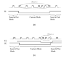
- FIG. 14 is a diagram illustrating a test cycle of a scan test.
- the test of the combinational circuit part of the full scan sequential circuit is performed by repeating scan shift and scan capture.
- SE shift mode
- one or more clock pulses are applied, and one or more new values are externally scanned into the scan flip-flops in the scan chain.
- one or more values existing in the scan flip-flop in the scan chain are scanned out.
- one clock pulse is simultaneously applied to all the scan flip-flops in one scan chain, and the values of the pseudo external output lines of the combinational circuit unit are taken out and held in all the scan flip-flops.
- Scan shift is used to input a test input pattern to the combinational circuit unit via the pseudo external input line and to extract a test response from the combinational circuit unit via the pseudo external output line.
- the scan capture is used for taking out and holding the test response of the combinational circuit unit in the scan flip-flop.
- the combinational circuit unit can be tested by repeating scan shift and scan capture for all test input patterns.
- FIG. 15 is a block diagram showing a failure detection system 101 as a background art of the present invention.
- the failure detection system 101 includes a take-out device 107, a determination device 111, and a pattern control device 113.
- the extraction device 107 includes an extraction unit 117 and a storage unit 121.
- the determination device 111 includes a comparison unit 129 and a failure determination unit 131.
- the pattern control device 113 includes a test input pattern holding unit 133, a development circuit 135, and a compression circuit 137.
- a test input pattern is inputted to the combinational circuit unit 3 directly from an external input and by a scan shift. Any logic value can be set in any scan flip-flop by the scan shift, so that the problem of controllability of the pseudo external input line is solved.
- Extraction of the test response from the combinational circuit unit 3 includes a part directly performed from an external output and a part performed by scan shift.
- the extraction unit 117 can extract the output value of an arbitrary scan flip-flop, so that the problem of observability of the pseudo external output line is solved. Note that the number of scan flip-flops is usually equal to the number of pseudo external output lines.
- the comparison unit 129 compares the extracted value with a value predicted when the combinational circuit unit 3 is normal. Based on the comparison result, the failure determination unit 131 determines whether there is a failure in the combinational circuit unit 3.
- BIST Built-In Self-Test
- the storage capacity for storing test input patterns is particularly limited. Therefore, methods for reducing the amount of test data have been developed.
- One example is a method of compressing a test input pattern and treating it as a seed pattern (seed).
- seed is expanded before being scanned in. It is also compressed before being scanned out. Therefore, the amount of test data can be reduced. However, along with the increase in the scale of semiconductor integrated circuits, further reduction in the amount of test data is required.
- FIG. 16 is a diagram showing a test cycle of the multi-capture method.
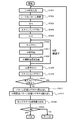
- FIG. 17 is a flowchart showing a procedure when the conventional multi-capture method is used.
- the circuit size is reduced by reducing the number of flip-flops designed for scan.
- the input logical value corresponding to the flip-flop that is not designed for scanning is not fixed. Then, even if the output logical value is taken out, there is little information obtained about the failure, so the failure detection rate is lowered.
- each test input pattern is captured multiple times in the capture mode. That is, the logical value acquired by the flip-flop 5 of FIG. 15 is newly input to the combinational circuit unit 3 as an input test pattern. Then, the value captured by the flip-flop 5 is gradually determined each time the combinational circuit unit 3 is passed. Eventually, the logical values of all flip-flops 5 are determined. Therefore, a confirmed test output pattern is obtained for the confirmed test input pattern. As a result, it is possible to maintain the failure detection rate even in the semiconductor integrated circuit of the partial scan design.
- the seed input is started (step ST501), and the seed is developed by the development circuit 135 (step ST502).
- the shift mode is started (step ST503), and the test input pattern is scanned into the flip-flop 5 (step ST504).
- the capture mode is started (step ST505), and the capture is repeated a predetermined number of times (step ST506).
- the value of the test input pattern is gradually determined.
- the shift mode is started again (step ST507), and the logic value of the flip-flop 5 is scanned out (step ST508).
- step ST501 the process returns to step ST501, and if not, the process proceeds to the next (step ST509).
- the extraction unit 117 extracts the compressed data (signature) scanned out (step ST510).
- the comparison unit 129 compares the obtained signature with the signature predicted when the combinational circuit unit 3 is normal (step ST511). Based on the comparison result, failure determination unit 131 determines whether or not there is a failure in combinational circuit unit 3 (step ST512).
- the amount of test data that the test pattern holding unit 133 should store is proportional to the number of test input patterns.
- the number of test output patterns is equal to the number of test input patterns.
- the failure detection rate is positively correlated with the number of test output patterns. Therefore, when the number of test input patterns is reduced, the failure detection rate is lowered. Therefore, the number of test input patterns cannot be reduced in order to maintain the failure detection rate. As a result, the amount of test data could not be reduced.
- an object of the present invention is to provide a failure detection system or the like that improves the failure detection rate while reducing the amount of test data of test input patterns to be stored.
- a first aspect of the present invention is a failure detection system that detects a failure of a logic circuit based on a plurality of output logic values output from a logic circuit to which a test input pattern is input, the plurality of output logics The value is input as a new test input pattern to the logic circuit, and a first extraction unit that extracts part or all of the plurality of output logical values, and an output that is extracted by the first extraction unit Comparison means for comparing a logical value with an output logical value predicted when there is no failure in the logic circuit or an output logical value predicted when there is a specific failure, and based on a comparison result by the comparison means
- a failure detection system comprising failure determination means for determining the presence or absence of a failure in the logic circuit.
- a second aspect of the present invention is the failure detection system according to the first aspect, wherein the plurality of output logical values are held in holding means for holding the logical values one by one in a plurality of individual holding means,
- the first extracting means extracts part or all of the plurality of output logic values held in the holding means, and part or all of the output logic values held by the plurality of individual holding means are Take out directly without going through individual holding means.
- the failure detection system includes the new test input pattern after the holding means holds the plurality of output logical values. Until a plurality of new output logic values output from the logic circuit to which the input is received are held in the holding means, part or all of the plurality of output logic values held in the holding means Take out.
- a fourth aspect of the present invention is the failure detection system according to the third aspect, wherein the holding means holds the output logic value and then the new test input pattern is output from the logic circuit. Control means for controlling the time until a plurality of new output logic values are held in the holding means is further provided.
- the failure detection system according to any one of the second to fourth aspects, wherein the output logic value held in each of the individual holding means calculates a contribution to failure detection. And a ranking means for ranking each individual holding means based on the magnitude of the contribution, wherein the first take-out means includes the output logical values held by the plurality of individual holding means. Only a predetermined number is taken out based on the ranking.
- a sixth aspect of the present invention is the failure detection system according to any one of the second to fifth aspects, wherein some or all of the output logical values held by the plurality of individual holding means are held separately by another A second take-out means for taking out via the means, the comparing means, the output logic value taken out by the second take-out means and an output logic value predicted when there is no failure in the logic circuit or a specific value Comparison is also made with the predicted output logic value when there is a failure, and the number of times the first take-out means takes out the output logic value is greater than or equal to the number of times the second take-out means takes out the output logic value. is there.
- a seventh aspect of the present invention is the failure detection system according to any one of the first to sixth aspects, wherein the first compression means for compressing the data size of the output logical value and the output logical value are stored.
- a first storage means and in synchronization with the extraction process of the first extraction means, the first compression means compresses the output logical value extracted by the first extraction means, and the first storage means Stores the output logical value compressed by the first compression means.
- an extracting device for extracting a part or all of a plurality of output logic values output from a logic circuit to which a test input pattern is input, wherein the plurality of output logic values are logic values.
- the holding means has a plurality of individual holding means for holding logical values one by one. Then, some or all of the output logical values held by the plurality of individual holding means are directly extracted without going through other individual holding means.
- an extracting device for extracting a part or all of a plurality of output logic values output from a logic circuit to which a test input pattern is input, wherein the plurality of output logic values are logic values. And a new test input pattern that is input to the logic circuit. After the holding means holds the output logic value, the new test input pattern is Control means for controlling the time until a plurality of new output logic values output from the input logic circuit are held in the holding means, and the plurality of output logic values held in the holding means Remove some or all.
- a failure detection method for detecting a failure of a logic circuit based on a plurality of output logic values output from the logic circuit to which a test input pattern is input.
- a first input step in which a test input pattern is input; a holding unit that holds a plurality of logical values one by one in a plurality of individual holding units; a holding step that holds the plurality of output logical values; and the holding unit holds A second input step in which the plurality of output logic values are input to the logic circuit as a new test input pattern; and after the holding means holds the plurality of output logic values, the new test
- the plurality of individual holding means hold until a plurality of new output logic values output from the logic circuit to which the input pattern is inputted are held in the holding means.
- a first extraction step in which some or all of the plurality of output logic values are directly extracted without going through other individual holding means, and part of the plurality of output logic values held by the plurality of individual holding means or Predicted when there is no failure in the second extraction step, all of which is extracted via other individual holding means, the output logic values extracted in the first extraction step and the second extraction step, and the logic circuit.
- An eleventh aspect of the present invention is the failure detection method according to the tenth aspect, wherein the first extraction step is synchronized with the first extraction step between the first extraction step and the second extraction step.
- a first compression step in which the output logical value extracted in the extraction step is compressed; and a first storage step in which the output logical value compressed in the compression step is stored; The storage step is repeated a predetermined number of times.
- a twelfth aspect of the present invention is the failure detection method according to the eleventh aspect, wherein the control means holds the output logic value between the first storage step and the holding step. And a control step of controlling time until a plurality of new output logic values output from the logic circuit to which the new test input pattern is input are held in the holding means.
- a thirteenth aspect of the present invention is the failure detection method according to the twelfth aspect, wherein in the control step, the control means holds the new test input pattern after the holding means holds the output logic value. The time until a plurality of new output logic values output from the input logic circuit are held in the holding means is shortened.
- a failure detection method for detecting a failure of a logic circuit based on a plurality of output logic values output from the logic circuit to which a test input pattern is input.
- a first input step in which a test input pattern is input, a holding step in which the holding means holds the plurality of output logic values, and the plurality of output logic values held in the holding means are used as new test input patterns.
- the control means receives a plurality of new output logic values output from the logic circuit to which the new test input pattern is input after the holding means holds the output logic value in the holding means. Including a control step for controlling the time until the hold.
- a fifteenth aspect of the present invention is a program that allows a computer connected to the holding means to execute the failure detection method according to any one of the tenth to fourteenth aspects.
- a sixteenth aspect of the present invention is a computer-readable recording medium that can be executed by a computer connected to the holding means, and is a recording medium that records a program according to the fifteenth aspect.
- the failure detection system may further include initial pattern storage means for storing an initial test input pattern.
- the pattern stored by the initial pattern storage means may be a seed pattern (seed) in which the initial test input pattern is compressed.
- the failure detection system may include a developing unit that expands the seed pattern.
- the failure detection system may include a second compression unit that compresses the output logical value extracted by the second extraction unit.
- one compression means may serve as both the first compression means and the second compression means.
- the failure detection system according to the invention of each claim of the present application may include second storage means for storing the output logical value extracted by the second extraction means. Further, one storage unit may serve as both the first storage unit and the second storage unit.
- test output patterns it is possible to obtain a plurality of test output patterns from one initial test input pattern by the extracting means or the extracting device. This is because the test output pattern obtained at each capture is input to the logic circuit as a new test input pattern different from the initial test input pattern.
- the test data amount is expressed by Expression (3) as in the conventional case.
- the number of test output patterns is expressed by equation (4).
- test data amount is directly proportional to the number of initial test input patterns regardless of the number of captures. Therefore, by increasing the number of captures, it is possible to improve the failure detection rate while reducing the number of test input patterns to be stored by reducing the number of initial test input patterns.
- FIG. 18 is a time development diagram showing an example in the case of using the conventional multi-capture method.
- FIG. 18 shows a flow of logic values from immediately after the initial test input pattern is scanned in to the second capture in the shift mode.
- the flip-flop 5 3 should retain the logic value 0.
- the failure of the NOR gate e.g. delay fault
- the first flip-flop 3 after capture is assumed to hold the logical value 1.
- the logical value of the flip-flop 3 is unless the shift mode is captured a predetermined number of times (here, twice), has not been taken.
- flip-flop 3 holds the same 0 if successful. Therefore, in the conventional method, this NOR gate failure was not detected.
- the value held by the holding means after the first capture is taken out by the extracting means or the extracting device. This makes it possible to detect a failure that can be detected only by another test input pattern by the conventional method, by using the same initial test input pattern. Therefore, the required amount of storage capacity can be reduced.
- the first take-out means takes out the output logical value directly from each individual holding means. Therefore, even when there are a large number of external output lines and individual holding means, it is possible to quickly extract the output logical value desired to be extracted. In addition, when the output logical value is extracted, the logical value held by the other individual holding means can be extracted without being overwritten.
- the first fetching means is synchronized with the holding of the output logic value by the holding means (after the holding means holds the output logic value, a new test input pattern is The output logic value held in the holding means is taken out until a plurality of new output logic values output from the input logic circuit are held in the holding means. For this reason, the first take-out means can reliably take out the value taken out and held by the holding means at each capture without being overwritten with the output logic value to be captured next.
- the fourth, ninth, twelfth, or fourteenth aspect of the present invention it is possible to detect only stuck-at faults by increasing the clock period and to detect delay faults by shortening the clock period. It becomes. This makes it possible to obtain information that contributes to failure cause analysis and debugging.
- a delay failure is detected by shortening the clock cycle.
- a test input pattern that causes only a small number of transitions can be obtained by repeating the input of the pattern output from the test target circuit in the capture cycle to the circuit as a test input pattern 2-3 times. It has been. For this reason, it becomes possible to detect delay faults with high accuracy by reducing power consumption and noise during capture.
- the first extraction means it is possible for the first extraction means to focus on the value held by the holding means that is particularly effective for a predetermined purpose, for example, to improve the failure detection rate. Become. Therefore, the failure detection rate can be improved more efficiently. That is, the amount of test data can be further reduced. In addition, the amount of data to be output can be reduced as compared with the case where values held by all the holding means are extracted in synchronization with the holding process of the holding means. Furthermore, the circuit size can be reduced.
- the number of clock pulses given during scan shift is generally large for one test input pattern.
- the multi-capture method even if several to tens of clocks are given in the capture mode, most of the test time is spent in the shift mode.
- the test time could not be reduced because the number of test input patterns to be scanned in could not be reduced.
- the time of the shift mode can be shortened.
- the scan-in time is shortened by reducing the number of initial test input patterns to be scanned-in. Therefore, the test time can be shortened.
- test time is in contrast to the increase in test time as a result of spending many test input patterns to improve the failure detection rate.
- shortening the test time is particularly important.
- the first take-out means taking out in synchronization with the holding of the holding means in the capture mode takes out the test output more frequently than the second take-out means taking out in the shift mode. That is, the scan-out time can be shortened. Therefore, it becomes easy to further shorten the test time.
- the extraction process, the compression process, and the storage process are performed in synchronization with the holding process and the test process. Therefore, as compared with the case of storing in the shift mode, a large amount of data taken out by multi-capture can be quickly stored in the capture mode. Therefore, the number of patterns to be scanned out can be reduced, and the test time can be further shortened. In addition, it becomes easier to reduce the amount of output data.
- FIG. 6 is a flowchart showing an example of a procedure for selecting a flip-flop 5 by the selection device 9. It is a graph which shows an example of the experimental result at the time of using the failure detection system of FIG. It is a graph which shows the relationship between the number of test vectors, and a failure detection rate. It is a figure which shows the relationship between the ratio of the flip-flop which takes out a logical value, and the overhead of a circuit.
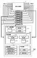
- FIG. 1 is a block diagram showing an example of a failure detection system according to an embodiment of the present invention.
- the failure detection system 1 is a failure detection system that detects a failure in the combinational circuit unit 3 based on a plurality of output logic values output from the combinational circuit unit 3 (an example of “logic circuit” in the claims of the present application).
- the combinational circuit unit 3 is connected to a plurality of flip-flops 5 1 to 5 7 (an example of “individual holding means” in the claims) that holds a plurality of output logic values.
- Each flip-flop 5 holds one logical value.
- the subscript is omitted and referred to as “flip-flop 5”.
- the plurality of flip-flops 5 are collectively referred to as a holding unit 4 (an example of “holding unit” in the claims of the present application).
- the failure detection system 1 uses a multi-capture method, similarly to the conventional failure detection system 101 shown in FIG.
- the failure detection system 1 includes an extraction device 7 (an example of “extraction means” in the claims of the present application), a selection device 9, a determination device 11, and a pattern control device 13.
- the extracting device 7 extracts part or all of the output logical value held by the flip-flop 5.
- the selection device 9 selects a flip-flop from which the extraction means 7 should mainly extract a value.
- the determination device 11 compares the extracted output logic value with the predicted value, and determines whether or not the combinational circuit unit 3 has failed.
- the pattern control device 13 controls the test input pattern to the combinational circuit unit 3 and the size of the test output pattern from the combinational circuit unit 3.
- the take-out device 7 includes a capture mode take-out section 15 (an example of “first take-out means” in the claims of the present application), a shift mode take-out section 17 (an example of “second take-out means” in the claims of the present application), and a capture mode storage.
- a unit 19 an example of “first storage unit” in the claims of the present application
- a shift mode storage unit 21 an example of “second storage unit” in the claims of the present application
- the capture mode extraction unit 15 performs a capture process in which the flip-flop 5 captures a plurality of output logical values in the capture mode (an example of “holding process” in the claims of the present application) and a test of the combinational circuit unit 3 based on a new test input pattern In synchronization with the process (an example of “test process” in the claims of the present application), a part or all of the output logical value is extracted.
- taking out synchronously means that the flip-flop 5 takes out the output logic value after it captures the next output logic value.
- the capture mode extraction unit 15 uses a part or all of the output logic value held by the flip-flop 5 i (1 ⁇ i ⁇ 7) as another flip-flop 5 k (1 ⁇ k ⁇ 7, k ⁇ i). Take out directly without going through. Further, the capture mode extraction unit 15 stores the extracted output logic value in the capture mode storage unit 19.
- the shift mode extraction unit 17 extracts a value scanned out by the flip-flop 5 in the shift mode.
- the extracted output logic value is stored in the shift mode storage unit 21.
- the extraction of the shift mode extraction unit 17 is performed after all the test processes are completed, for example, and is not synchronized with the capture process and the test process.
- the shift mode extraction unit 17 converts a part or all of the output logic values held by the flip-flops 5 i (1 ⁇ i ⁇ 7) to other flip-flops 5 k (1 ⁇ k ⁇ 7, k ⁇ i). Take out via.
- the selection device 9 includes a simulation unit 23, a calculation unit 25 (an example of “calculation unit” in the claims of the present application), and a ranking unit 27 (an example of “ranking unit” in the claims of the present application).
- the simulation unit 23 performs a failure simulation of the combinational circuit unit 3.
- the calculation unit 25 calculates the contribution of each flip-flop 5 to the failure detection based on the result of the failure simulation.
- the ranking unit 27 ranks each flip-flop 5 based on the magnitude of contribution.
- the determination device 11 includes a comparison unit 29 and a failure determination unit 31.
- the comparison unit 29 compares the extracted value with the predicted value.
- the predicted value may be a value predicted to be an output logical value when there is no failure in the combinational circuit unit 3, or an output logical value when there is a specific failure in the combinational circuit unit 3. It may be a value predicted to be present.
- the failure determination unit 31 determines whether there is a failure in the combinational circuit unit 3 based on the comparison result.
- the pattern control device 13 includes an initial test input pattern holding unit 33, a development circuit 35, and a compression circuit 37.
- the initial test input pattern holding unit 33 includes a test pattern input to the combinational circuit unit 3. This initial test input pattern may be a compressed seed pattern (seed).
- seed seed
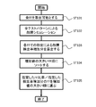
- FIG. 2 is a flowchart showing an example of a procedure when the failure detection system 1 is used.
- step ST001 one of seeds included in the initial test input pattern holding unit 33 is selected, and input to the combinational circuit unit 3 is started.
- step ST002 the selected seed is developed by the development circuit 35.
- step ST003 the scan enable signal is set to 1, and the shift mode is set.
- step ST004 the developed initial test input pattern is scanned into the flip-flop 5 in accordance with the clock signal.
- step ST005 the scan enable signal is set to 0 and the capture mode is set.
- step ST006 the flip-flop 5 captures the output logical value from the combinational circuit unit 3 in accordance with the clock signal.
- step ST007 the capture mode extraction unit 15 extracts the value held by the flip-flop 5 in synchronization with the capture processing of the flip-flop 5. Further, the flip-flop 5 gives the value to be held to the combinational circuit unit 3 as a new test input pattern. Further, the combinational circuit unit 3 performs a test process based on the given new test input pattern.
- the capture mode extraction unit 15 performs “intermediate extraction” for extracting the output logical value in the middle of the capture mode.
- output logical values are extracted only in the shift mode following the capture mode, and are not extracted in the capture mode.
- the flip-flop 5 from which the value is extracted by the capture mode extraction unit 15 is limited to the flip-flop selected by the selection device 9 (in this embodiment, 5 3 , 5 5 , 5 7 ). As a result, the failure detection rate per test time can be improved. The procedure for selecting the flip-flop will be described later.
- step ST008 the value extracted by the capture mode extraction unit 15 is compressed by the compression circuit 37 to reduce the data size, and stored in the capture mode storage unit 19. Steps ST006 to ST008 are repeated a predetermined number of times (N times), and then the process proceeds to the next step.
- step ST009 the scan enable signal is set to 1 and the shift mode is set.
- step ST010 the value held in the flip-flop 5 is scanned out to the shift mode extraction unit 17 in accordance with the clock signal. The scanned-out value is compressed by the compression circuit 37 and stored in the shift mode storage unit 21.
- the extraction by the shift mode extraction unit 17 is extraction in the shift mode, it is not synchronized with the capture process and the test process. A lot of time is required for taking out in the shift mode. Therefore, the entire test time can be shortened by setting the number of extractions by the capture mode extraction unit 15 to be at least the number of extractions by the shift mode extraction unit 17.
- step ST011 the determination device 11 determines whether or not there is an uninput seed in the initial test input pattern holding unit 33. If there is an uninput seed, the process returns to step ST001. If there is no uninput seed, proceed to the next step.
- step ST012 the determination apparatus 11 reads the compressed data (signature) stored in the capture mode storage unit 19. At the same time, in step ST013, the determination apparatus 11 also reads out the signature stored in the shift mode storage unit 21.
- the comparison unit 29 compares the read value with a value predicted when the combinational circuit unit 3 is normal or a value predicted when there is a specific failure.
- the failure determination unit 31 determines whether there is a failure in the combinational circuit unit 3 based on the comparison result by the comparison unit 29.
- FIG. 3 is a time development view showing an example when the failure detection system 1 is used.
- failure detection system 1 By using the failure detection system 1, it is possible to detect a failure of the failed NOR element A indicated by A in FIG. An output logical value of the flip-flop 5 3 After 1st Capture Capture Mode extraction unit 15 because taken. If NOR element is normal, it is 0 as an output logical value of the flip-flop 5 3 After 1st capture is taken out. On the other hand, if the NOR element has failed, 1 is taken out.
- the shift mode extraction unit 17 extracts all the values of the flip-flops 5 in the shift mode, the output logic value extracted is less than that of the conventional failure detection system. As a result, the failure detection rate is improved by the test output pattern extracted by the capture mode extraction unit 15.
- FIG. 4 is a flowchart showing an example of a procedure in which the selection device 9 selects the flip-flop 5.
- step ST101 the values of all flip-flops 5 can be taken out.
- step ST102 the simulation unit 23 performs a failure simulation using all the test input patterns.
- step ST103 the calculation unit 25 calculates an increase in the failure detection rate by taking out the value of each flip-flop 5 (an example of “contribution” in the claims of the present application).
- step ST104 the ranking unit 27 ranks the flip-flops 5 in descending order of increase in the failure detection rate.
- step ST ⁇ b> 105 the selection device 9 selects the flip-flop 5 that particularly contributes to the improvement of the failure detection rate based on the ranking given to the flip-flop 5.
- the capture mode extraction unit 15 may extract only the value of the flip-flop 5 up to a predetermined order.
- connection here may be any means as long as it is electrically connected. For example, turning on a switch that has been turned off is included, and physically connecting is also included.
- the capture mode extraction unit 15 can extract only the value of the flip-flop 5 that is particularly efficient. By increasing the efficiency of fault detection, the amount of test data can be further reduced.
- FIG. 5 is a graph showing an example of an experimental result when the failure detection system 1 is used.
- the horizontal axis indicates the ratio of the flip-flops 5 from which values are extracted by the capture mode extraction unit 15.
- the vertical axis represents the failure detection rate.
- the failure detection rate is improved as the ratio of the flip-flops 15 connected to the capture mode extraction unit 15 is increased.
- the increase rate of the fault detection rate slope of the graph
- the increase in the fault detection rate is saturated above a certain ratio. This also shows that an efficient flip-flop can be selected to improve the failure detection rate.
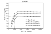
- FIG. 6 is a graph showing the relationship between the number of test vectors and the failure detection rate.
- the horizontal axis represents the number of test vectors, and the vertical axis represents the failure detection rate.
- FIG. 6 shows a case where intermediate extraction is not performed and a case where 20%, 50% and 100% flip-flops 5 are captured five times and intermediate extraction is performed.
- the failure detection rate is improved by performing intermediate extraction. It is also shown that the failure detection rate is improved by performing intermediate extraction of more flip-flop values. In addition, it can be seen that it is effective to perform intermediate extraction only for 20% of the flip-flops 5.
- the failure detection method according to the embodiment of the present invention can be used in addition to the conventional method. Therefore, it is possible to further improve the failure detection rate obtained by the conventional method while reducing the amount of test data of the test input pattern.
- FIG. 7 is a diagram illustrating the relationship between the ratio of flip-flops that extract logical values and the overhead of the circuit.
- the horizontal axis represents the proportion of flip-flops 5 that perform intermediate extraction.
- the vertical axis represents the ratio of circuit overhead.
- the overhead of the circuit increases almost in direct proportion to the proportion of flip-flops 5 that perform intermediate extraction.
- the overhead increase is 9.3%.
- the overhead increase is only 2.0%. Therefore, it is possible to improve the failure detection rate while suppressing an increase in overhead by selecting flip-flops as necessary and performing intermediate extraction.
- the clock cycle includes a plurality of new output logics output from the combinational circuit unit 3 to which a new test input pattern is input after the flip-flop 5 holds the plurality of output logical values from the combinational circuit unit 3. This corresponds to the time until the value is held in the flip-flop 5.
- FIG. 8 is a block diagram showing an example of a failure detection system that can change the clock cycle.
- FIG. 9 is a diagram showing a test cycle when the clock period is changed in the capture mode.
- FIG. 9A illustrates a case where a failure is detected with all clocks
- FIG. 9B illustrates a case where only a delay failure is detected.
- the failure detection system 201 has the same configuration as that of the failure detection system 1 in FIG. 1 except that the failure detection system 201 includes a clock control unit 218 (an example of “control means” in the claims of the present application).
- the clock control unit 218 controls the cycle in which the flip-flop 5 captures the output logic value from the combinational circuit unit 3 and the cycle in which the value held by the flip-flop 5 is given to the combinational circuit unit 3 as a new test input pattern. .
- a test input pattern is given multiple times to the combinational circuit unit 3 which is a test target circuit.
- the ratio (toggle rate) at which the logic values of the elements in the combinational circuit unit 3 transition is greatly reduced by the input of the test input pattern after about the third time.
- the toggle rate is smaller in a scan test than in a random test input pattern, and even smaller in normal user use.
- the random test input pattern is about 50%
- the scan test is about 20-30%
- the normal use of the user is about 5%.
- test input pattern has already been passed through the combinational circuit unit 4 four times. Therefore, the test input pattern has a low toggle rate, and an excessive change in voltage is less likely to occur even if the clock cycle is shortened. Therefore, it is possible to reduce power consumption and noise accompanying delay fault detection.
- the capture mode extraction unit 215 may be controlled by the capture enable signal line (CE).
- CE the capture enable signal line
- SCOAP Synchronization Observability Analysis Program
- FIG. 10 is a block diagram showing an example of a failure detection system using SCOAP analysis.
- the failure detection system 301 includes a controllability calculation unit 324 and an observability calculation unit 326 (a controllability calculation unit 324 and an observability calculation unit 326) instead of the simulation unit 23 and the calculation unit 25 of FIG. 1.
- the controllability calculation unit 324 calculates the controllability of the elements in the combinational circuit unit 3.
- the observability calculation unit 326 calculates the observability of the elements in the combinational circuit unit 3 and the flip-flop 5.
- the ranking unit 327 ranks the flip-flops 5 in descending order of the calculated observability. Comparison and failure determination are performed in the same manner as the failure detection system 1 in FIG.
- FIG. 11 is a diagram showing a list of failure detection rates when FFs are ranked by three selection methods and intermediate extraction is performed.
- FIG. 12 is a diagram showing a comparison of time required for ranking flip-flops. As shown in FIG. 12, when the flip-flop 5 is selected using the SCOAP analysis, the required CPU time is significantly shortened compared to the case where the simulation is used.
- step ST004 scan-in and scan-out may be performed simultaneously. That is, in step ST004, the developed initial test input pattern is scanned into the flip-flop 5 in accordance with the clock signal, and at the same time, the value held in the flip-flop 5 is scanned out to the shift mode extracting unit 17. It may be done. By performing the scan-in and the scan-out simultaneously, it is possible to shorten the shift mode time. The same applies to step ST010.
- step ST008 in the flow of FIG. 2 either the storage process by the capture mode storage unit 19 or the compression process by the compression circuit 37 may be performed first. Further, the capture mode extraction unit 15 may extract the output compressed by the compression circuit 37. The same applies to the processing order of the shift mode extraction unit 17, the shift mode storage unit 21, and the compression circuit 37.
- step ST012 may be executed together with step ST004 in the iterative process following step ST011. Furthermore, although there is a possibility that the test time will be longer, the processing of step ST012 may be included in the repeated processing of the processing from step ST006 to step ST008. The process from step ST013 to step ST015 is the same as step ST012.
- the initial test input pattern holding unit 33 may include a test pattern generator such as a linear feedback shift register (LFSR).
- LFSR linear feedback shift register
- the initial test input pattern may be developed by the LFSR generating new seeds one after another based on the seed of the initial test input pattern holding unit 33.
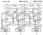
- the compression circuit 37 may be, for example, a multi-input signature register (MISR) that compresses output logical values from N scan chains into N-bit signatures. By using the MISR exemplified in FIG. 13, as shown in FIG. 7, even if the number of flip-flops for extracting values increases, the overhead of the circuit is only increased by about 0.2%.
- the compression circuit may be provided in the take-out device.
- failure detection can be performed on the premise of the configuration of the conventional scan circuit.
- the test output pattern from the logic circuit to be tested may be bifurcated. At this time, it becomes possible to output the test output pattern to the extracting device in synchronization with the input of one output as a new test input pattern to the logic circuit to be tested. Accordingly, no holding means is required.
- a part or all of the failure detection system 1 may be incorporated in a semiconductor logic circuit having the combinational circuit unit 3 and the flip-flop 5, or may be realized as a tester, or a part thereof may be a semiconductor logic. Another part of the circuit may be implemented as a tester.
Landscapes
- Physics & Mathematics (AREA)
- General Physics & Mathematics (AREA)
- Engineering & Computer Science (AREA)
- General Engineering & Computer Science (AREA)
- Tests Of Electronic Circuits (AREA)
- Semiconductor Integrated Circuits (AREA)
Abstract
Description



Claims (16)
- テスト入力パターンが入力された論理回路から出力された複数の出力論理値に基づいて当該論理回路の故障を検出する故障検出システムであって、
前記複数の出力論理値は、前記論理回路に対して新たなテスト入力パターンとして入力されるものであり、
前記複数の出力論理値の一部又は全部を取り出す第1取出手段と、
前記第1取出手段が取り出した出力論理値と、前記論理回路に故障がない場合に予測される出力論理値又は特定の故障がある場合に予測される出力論理値とを比較する比較手段と、
前記比較手段による比較結果に基づいて前記論理回路の故障の有無を判定する故障判定手段とを備える、故障検出システム。 - 前記複数の出力論理値は、複数の個別保持手段に論理値を1つずつ保持させる保持手段に保持され、
前記第1取出手段は、
前記保持手段に保持された前記複数の出力論理値の一部又は全部を取り出すものであり、
前記複数の個別保持手段が保持する出力論理値の一部又は全部を、他の個別保持手段を経由することなく直接取り出す、請求項1記載の故障検出システム。 - 前記第1取出手段は、前記保持手段が前記複数の出力論理値を保持してから、前記新たなテスト入力パターンが入力された前記論理回路から出力された新たな複数の出力論理値が前記保持手段に保持されるまでの間に、前記保持手段に保持された前記複数の出力論理値の一部又は全部を取り出す、請求項2記載の故障検出システム。
- 前記保持手段が前記出力論理値を保持してから前記新たなテスト入力パターンが入力された前記論理回路から出力された新たな複数の出力論理値が前記保持手段に保持されるまでの時間を制御する制御手段をさらに備える、請求項3記載の故障検出システム。
- 各前記個別保持手段に保持された前記出力論理値の故障検出への寄与を算出する算出手段と、
前記寄与の大きさに基づいて各前記個別保持手段に順位を付ける順位付け手段とをさらに備え、
前記第1取出手段は、前記複数の個別保持手段が保持する前記出力論理値のうち、前記順位に基づいて所定の個数のみを取り出す、請求項2から4のいずれかに記載の故障検出システム。 - 前記複数の個別保持手段が保持する出力論理値の一部又は全部を、他の個別保持手段を経由させて取り出す第2取出手段をさらに備え、
前記比較手段は、前記第2取出手段が取り出した出力論理値と、前記論理回路に故障がない場合に予測される出力論理値又は特定の故障がある場合に予測される出力論理値との比較も行うものであり、
前記第1取出手段が前記出力論理値を取り出す回数は、前記第2取出手段が前記出力論理値を取り出す回数以上である、請求項2から5のいずれかに記載の故障検出システム。 - 前記出力論理値のデータサイズを圧縮する第1圧縮手段と、
前記出力論理値を記憶する第1記憶手段とをさらに備え、
前記第1取出手段の取出処理と同期して、
前記第1圧縮手段は、前記第1取出手段が取り出した前記出力論理値を圧縮し、
前記第1記憶手段は、前記第1圧縮手段が圧縮した前記出力論理値を記憶する、請求項1から6のいずれかに記載の故障検出システム。 - テスト入力パターンが入力された論理回路から出力された複数の出力論理値の一部又は全部を取り出す取出装置であって、
前記複数の出力論理値は、論理値を保持する保持手段により保持されると共に、前記論理回路に対して新たなテスト入力パターンとして入力されるものであり、
前記保持手段は、論理値を1つずつ保持する複数の個別保持手段を有し、
前記複数の個別保持手段が保持する出力論理値の一部又は全部を、他の個別保持手段を経由することなく直接取り出す、取出装置。 - テスト入力パターンが入力された論理回路から出力された複数の出力論理値の一部又は全部を取り出す取出装置であって、
前記複数の出力論理値は、論理値を保持する保持手段により保持されると共に、前記論理回路に対して新たなテスト入力パターンとして入力されるものであり、
前記保持手段が前記出力論理値を保持してから前記新たなテスト入力パターンが入力された前記論理回路から出力された新たな複数の出力論理値が前記保持手段に保持されるまでの時間を制御する制御手段を備え、
前記保持手段に保持された前記複数の出力論理値の一部又は全部を取り出す、取出装置。 - テスト入力パターンが入力された論理回路から出力された複数の出力論理値に基づいて当該論理回路の故障を検出する故障検出方法であって、
前記論理回路に初期テスト入力パターンの入力が行われる第1入力ステップと、
複数の個別保持手段に論理値を1つずつ保持させる保持手段が、前記複数の出力論理値を保持する保持ステップと、
前記保持手段が保持する前記複数の出力論理値が、新たなテスト入力パターンとして前記論理回路に対して入力される第2入力ステップと、
前記保持手段が前記複数の出力論理値を保持してから、前記新たなテスト入力パターンが入力された前記論理回路から出力された新たな複数の出力論理値が前記保持手段に保持されるまでの間に、前記複数の個別保持手段が保持する前記複数の出力論理値の一部又は全部が他の個別保持手段を経由することなく直接取り出される第1取出ステップと、
前記複数の個別保持手段が保持する前記複数の出力論理値の一部又は全部が他の個別保持手段を経由して取り出される第2取出ステップと、
前記第1取出ステップ及び前記第2取出ステップにおいて取り出された出力論理値と、前記論理回路に故障がない場合に予測される出力論理値又は特定の故障がある場合に予測される出力論理値とを比較する比較ステップと、
前記比較ステップにおける比較結果に基づいて前記論理回路の故障の有無を判定する故障判定ステップとを含む、故障検出方法。 - 前記第1取出ステップと前記第2取出ステップとの間に、
前記第1取出ステップと同期して、前記第1取出ステップにおいて取り出された前記出力論理値が圧縮される第1圧縮ステップと、
前記圧縮ステップにおいて圧縮された前記出力論理値が記憶される第1記憶ステップとを備え、
前記保持ステップから前記第1記憶ステップまでが所定の回数だけ繰り返される、請求項10記載の故障検出方法。 - 前記第1記憶ステップと前記保持ステップの間に、制御手段が、前記保持手段が前記出力論理値を保持してから前記新たなテスト入力パターンが入力された前記論理回路から出力された新たな複数の出力論理値が前記保持手段に保持されるまでの時間を制御する制御ステップを含む、請求項11記載の故障検出方法。
- 前記制御ステップにおいて、制御手段が、前記保持手段が前記出力論理値を保持してから前記新たなテスト入力パターンが入力された前記論理回路から出力された新たな複数の出力論理値が前記保持手段に保持されるまでの時間を短縮する、請求項12記載の故障検出方法。
- テスト入力パターンが入力された論理回路から出力された複数の出力論理値に基づいて当該論理回路の故障を検出する故障検出方法であって、
前記論理回路に初期テスト入力パターンの入力が行われる第1入力ステップと、
前記複数の出力論理値を保持手段が保持する保持ステップと、
前記保持手段が保持する前記複数の出力論理値が、新たなテスト入力パターンとして前記論理回路に対して入力される第2入力ステップと、
前記複数の出力論理値の一部又は全部が取り出される取出ステップと、
前記取出ステップにおいて取り出された出力論理値と、前記論理回路に故障がない場合に予測される出力論理値又は特定の故障がある場合に予測される出力論理値とを比較する比較ステップと、
前記比較ステップにおける比較結果に基づいて前記論理回路の故障の有無を判定する故障判定ステップとを含み、
前記保持ステップと前記第2入力ステップが所定の回数だけ繰り返され、
前記第2入力ステップと前記保持ステップとの間に、制御手段が、前記保持手段が前記出力論理値を保持してから前記新たなテスト入力パターンが入力された前記論理回路から出力された新たな複数の出力論理値が前記保持手段に保持されるまでの時間を制御する制御ステップを含む、故障検出方法。 - 前記保持手段と接続されたコンピュータに、請求項10から14のいずれかに記載の故障検出方法を実行させることが可能なプログラム。
- 前記保持手段と接続されたコンピュータが実行することが可能なコンピュータに読み取り可能な記録媒体であって、請求項15記載のプログラムを記録する記録媒体。
Priority Applications (3)
| Application Number | Priority Date | Filing Date | Title |
|---|---|---|---|
| KR1020137008914A KR101891362B1 (ko) | 2010-10-05 | 2011-09-28 | 고장 검출 시스템, 취출 장치, 고장 검출 방법, 프로그램 및 기록 매체 |
| JP2012537651A JP5845187B2 (ja) | 2010-10-05 | 2011-09-28 | 故障検出システム、取出装置、故障検出方法、プログラム及び記録媒体 |
| US13/877,601 US9075110B2 (en) | 2010-10-05 | 2011-09-28 | Fault detection system, acquisition apparatus, fault detection method, program, and non-transitory computer-readable medium |
Applications Claiming Priority (2)
| Application Number | Priority Date | Filing Date | Title |
|---|---|---|---|
| JP2010225318 | 2010-10-05 | ||
| JP2010-225318 | 2010-10-05 |
Publications (1)
| Publication Number | Publication Date |
|---|---|
| WO2012046602A1 true WO2012046602A1 (ja) | 2012-04-12 |
Family
ID=45927597
Family Applications (1)
| Application Number | Title | Priority Date | Filing Date |
|---|---|---|---|
| PCT/JP2011/072211 Ceased WO2012046602A1 (ja) | 2010-10-05 | 2011-09-28 | 故障検出システム、取出装置、故障検出方法、プログラム及び記録媒体 |
Country Status (4)
| Country | Link |
|---|---|
| US (1) | US9075110B2 (ja) |
| JP (1) | JP5845187B2 (ja) |
| KR (1) | KR101891362B1 (ja) |
| WO (1) | WO2012046602A1 (ja) |
Cited By (5)
| Publication number | Priority date | Publication date | Assignee | Title |
|---|---|---|---|---|
| WO2013175998A1 (ja) * | 2012-05-23 | 2013-11-28 | 国立大学法人 九州工業大学 | 故障検出システム、生成回路及びプログラム |
| JP2020134303A (ja) * | 2019-02-19 | 2020-08-31 | 国立大学法人 大分大学 | 回路診断テスト装置、及び回路診断テスト方法 |
| WO2022014149A1 (ja) * | 2020-07-14 | 2022-01-20 | ソニーセミコンダクタソリューションズ株式会社 | 固体撮像素子、車両制御システム、および、固体撮像素子の制御方法 |
| CN114692674A (zh) * | 2022-02-21 | 2022-07-01 | 武汉船用电力推进装置研究所(中国船舶重工集团公司第七一二研究所) | 一种船舶推进系统故障判断方法及系统 |
| CN117409816A (zh) * | 2023-12-14 | 2024-01-16 | 湖南华夏特变股份有限公司 | 一种基于声音信号的设备故障检测方法及系统 |
Families Citing this family (4)
| Publication number | Priority date | Publication date | Assignee | Title |
|---|---|---|---|---|
| WO2012046602A1 (ja) * | 2010-10-05 | 2012-04-12 | 国立大学法人 九州工業大学 | 故障検出システム、取出装置、故障検出方法、プログラム及び記録媒体 |
| US9377511B2 (en) * | 2013-11-19 | 2016-06-28 | Infineon Technologies Ag | Coverage enhancement and power aware clock system for structural delay-fault test |
| JP6544958B2 (ja) * | 2015-03-18 | 2019-07-17 | ルネサスエレクトロニクス株式会社 | 半導体装置及び設計装置、スキャンフリップフロップ |
| CN115792584B (zh) * | 2023-02-07 | 2023-06-23 | 青岛青软晶尊微电子科技有限公司 | 基于大数据的集成电路实验方法及装置 |
Citations (3)
| Publication number | Priority date | Publication date | Assignee | Title |
|---|---|---|---|---|
| JP2005134180A (ja) * | 2003-10-29 | 2005-05-26 | Nec Electronics Corp | スキャンテスト方法、集積回路及びスキャンテスト回路 |
| JP2006012234A (ja) * | 2004-06-23 | 2006-01-12 | Toshiba Corp | メモリテスト回路およびメモリテスト方法 |
| JP2006058152A (ja) * | 2004-08-20 | 2006-03-02 | Toshiba Corp | 半導体装置の試験方法及び半導体装置の試験回路 |
Family Cites Families (13)
| Publication number | Priority date | Publication date | Assignee | Title |
|---|---|---|---|---|
| US5276893A (en) * | 1989-02-08 | 1994-01-04 | Yvon Savaria | Parallel microprocessor architecture |
| EP0584385B1 (en) * | 1992-08-25 | 1996-11-06 | International Business Machines Corporation | Method and system for testing an integrated circuit featuring scan design |
| US5550843A (en) * | 1994-04-01 | 1996-08-27 | Xilinx, Inc. | Programmable scan chain testing structure and method |
| US6662325B1 (en) * | 2000-10-05 | 2003-12-09 | Sun Microsystems, Inc. | Apparatus for on-line circuit debug using JTAG and shadow scan in a microprocessor |
| JP4228061B2 (ja) * | 2000-12-07 | 2009-02-25 | 富士通マイクロエレクトロニクス株式会社 | 集積回路の試験装置および試験方法 |
| US6836865B2 (en) * | 2001-10-09 | 2004-12-28 | International Business Machines Corporation | Method and apparatus for facilitating random pattern testing of logic structures |
| US7278080B2 (en) * | 2003-03-20 | 2007-10-02 | Arm Limited | Error detection and recovery within processing stages of an integrated circuit |
| JP2004301653A (ja) | 2003-03-31 | 2004-10-28 | Matsushita Electric Ind Co Ltd | 論理回路の故障解析方法 |
| US7007214B2 (en) * | 2003-06-30 | 2006-02-28 | International Business Machines Corporation | Diagnosable scan chain |
| DE102004059505B4 (de) * | 2004-12-10 | 2014-06-18 | X-Fab Semiconductor Foundries Ag | Anordnung zum Test von eingebetteten Schaltungen mit Hilfe von Testinseln |
| JP5035239B2 (ja) * | 2006-03-15 | 2012-09-26 | 日本電気株式会社 | 再構成可能デバイスのテストシステム及びその方法並びにそれに用いる再構成可能デバイス |
| US8819507B2 (en) * | 2010-05-10 | 2014-08-26 | Raytheon Company | Field programmable gate arrays with built-in self test mechanisms |
| WO2012046602A1 (ja) * | 2010-10-05 | 2012-04-12 | 国立大学法人 九州工業大学 | 故障検出システム、取出装置、故障検出方法、プログラム及び記録媒体 |
-
2011
- 2011-09-28 WO PCT/JP2011/072211 patent/WO2012046602A1/ja not_active Ceased
- 2011-09-28 KR KR1020137008914A patent/KR101891362B1/ko not_active Expired - Fee Related
- 2011-09-28 JP JP2012537651A patent/JP5845187B2/ja not_active Expired - Fee Related
- 2011-09-28 US US13/877,601 patent/US9075110B2/en active Active
Patent Citations (3)
| Publication number | Priority date | Publication date | Assignee | Title |
|---|---|---|---|---|
| JP2005134180A (ja) * | 2003-10-29 | 2005-05-26 | Nec Electronics Corp | スキャンテスト方法、集積回路及びスキャンテスト回路 |
| JP2006012234A (ja) * | 2004-06-23 | 2006-01-12 | Toshiba Corp | メモリテスト回路およびメモリテスト方法 |
| JP2006058152A (ja) * | 2004-08-20 | 2006-03-02 | Toshiba Corp | 半導体装置の試験方法及び半導体装置の試験回路 |
Cited By (12)
| Publication number | Priority date | Publication date | Assignee | Title |
|---|---|---|---|---|
| WO2013175998A1 (ja) * | 2012-05-23 | 2013-11-28 | 国立大学法人 九州工業大学 | 故障検出システム、生成回路及びプログラム |
| KR20150018551A (ko) * | 2012-05-23 | 2015-02-23 | 고쿠리츠 다이가쿠 호진 큐슈 코교 다이가쿠 | 고장 검출 시스템, 생성 회로 및 프로그램 |
| JPWO2013175998A1 (ja) * | 2012-05-23 | 2016-01-12 | 国立研究開発法人科学技術振興機構 | 故障検出システム、生成回路及びプログラム |
| US9383408B2 (en) | 2012-05-23 | 2016-07-05 | Japan Science And Technology Agency | Fault detection system, generation circuit, and program |
| KR101998452B1 (ko) * | 2012-05-23 | 2019-09-27 | 고쿠리츠켄큐카이하츠호진 카가쿠기쥬츠신코키코 | 고장 검출 시스템, 생성 회로 및 프로그램이 기록된 컴퓨터로 독출가능한 기록매체 |
| JP2020134303A (ja) * | 2019-02-19 | 2020-08-31 | 国立大学法人 大分大学 | 回路診断テスト装置、及び回路診断テスト方法 |
| JP7195602B2 (ja) | 2019-02-19 | 2022-12-26 | 国立大学法人 大分大学 | 回路診断テスト装置、及び回路診断テスト方法 |
| WO2022014149A1 (ja) * | 2020-07-14 | 2022-01-20 | ソニーセミコンダクタソリューションズ株式会社 | 固体撮像素子、車両制御システム、および、固体撮像素子の制御方法 |
| US12335648B2 (en) | 2020-07-14 | 2025-06-17 | Sony Semiconductor Solutions Corporation | Solid-state imaging device, vehicle control system, and control method for solid-state imaging device |
| CN114692674A (zh) * | 2022-02-21 | 2022-07-01 | 武汉船用电力推进装置研究所(中国船舶重工集团公司第七一二研究所) | 一种船舶推进系统故障判断方法及系统 |
| CN117409816A (zh) * | 2023-12-14 | 2024-01-16 | 湖南华夏特变股份有限公司 | 一种基于声音信号的设备故障检测方法及系统 |
| CN117409816B (zh) * | 2023-12-14 | 2024-03-26 | 湖南华夏特变股份有限公司 | 一种基于声音信号的设备故障检测方法及系统 |
Also Published As
| Publication number | Publication date |
|---|---|
| JP5845187B2 (ja) | 2016-01-20 |
| KR20140009974A (ko) | 2014-01-23 |
| US20130205180A1 (en) | 2013-08-08 |
| JPWO2012046602A1 (ja) | 2014-02-24 |
| KR101891362B1 (ko) | 2018-08-23 |
| US9075110B2 (en) | 2015-07-07 |
Similar Documents
| Publication | Publication Date | Title |
|---|---|---|
| JP5845187B2 (ja) | 故障検出システム、取出装置、故障検出方法、プログラム及び記録媒体 | |
| JP5537158B2 (ja) | 低消費電力スキャンテスト技術および装置 | |
| US11156661B2 (en) | Reversible multi-bit scan cell-based scan chains for improving chain diagnostic resolution | |
| US11073556B2 (en) | Low pin count reversible scan architecture | |
| CN114667455B (zh) | 用于测试电路的通用压缩器架构 | |
| CN112154336B (zh) | 确定性星体内建自测 | |
| US11408938B2 (en) | Bidirectional scan cells for single-path reversible scan chains | |
| JP6654456B2 (ja) | テストポイント回路、シーケンシャルテスト用スキャンフリップフロップ、半導体装置及び設計装置 | |
| US11150299B2 (en) | Flexible isometric decompressor architecture for test compression | |
| US10078114B2 (en) | Test point circuit, scan flip-flop for sequential test, semiconductor device and design device | |
| US10996273B2 (en) | Test generation using testability-based guidance | |
| US11442106B2 (en) | Method and apparatus for debugging integrated circuit systems using scan chain | |
| JP2013036903A (ja) | 故障箇所推定システム、故障箇所推定方法及び故障箇所推定用プログラム | |
| US11005458B2 (en) | Semiconductor integrated circuit adapted to scan testing, and method of designing the same | |
| JP5549622B2 (ja) | 故障診断方法、故障診断装置、テストシステム及びプログラム | |
| US11422188B2 (en) | Isometric control data generation for test compression | |
| Pomeranz | Concatenation of functional test subsequences for improved fault coverage and reduced test length | |
| CN120641984A (zh) | 单元感知链诊断 | |
| CN119024145A (zh) | 基于压缩的扫描测试系统 | |
| Pomeranz | Multipattern scan-based test sets with small numbers of primary input sequences | |
| Pomeranz | Compaction of a Transparent-Scan Sequence to Reduce the Fail Data Volume for Scan Chain Faults | |
| Pomeranz | Maintaining proximity to functional operation conditions under enhanced-scan tests based on functional broadside tests | |
| Moghaddam | On low power test and low power compression techniques |
Legal Events
| Date | Code | Title | Description |
|---|---|---|---|
| 121 | Ep: the epo has been informed by wipo that ep was designated in this application |
Ref document number: 11830535 Country of ref document: EP Kind code of ref document: A1 |
|
| DPE1 | Request for preliminary examination filed after expiration of 19th month from priority date (pct application filed from 20040101) | ||
| ENP | Entry into the national phase |
Ref document number: 2012537651 Country of ref document: JP Kind code of ref document: A |
|
| WWE | Wipo information: entry into national phase |
Ref document number: 13877601 Country of ref document: US |
|
| NENP | Non-entry into the national phase |
Ref country code: DE |
|
| ENP | Entry into the national phase |
Ref document number: 20137008914 Country of ref document: KR Kind code of ref document: A |
|
| 122 | Ep: pct application non-entry in european phase |
Ref document number: 11830535 Country of ref document: EP Kind code of ref document: A1 |