WO2012018079A1 - 太陽電池用インターコネクタ材、その製造方法及び太陽電池用インターコネクタ - Google Patents
太陽電池用インターコネクタ材、その製造方法及び太陽電池用インターコネクタ Download PDFInfo
- Publication number
- WO2012018079A1 WO2012018079A1 PCT/JP2011/067860 JP2011067860W WO2012018079A1 WO 2012018079 A1 WO2012018079 A1 WO 2012018079A1 JP 2011067860 W JP2011067860 W JP 2011067860W WO 2012018079 A1 WO2012018079 A1 WO 2012018079A1
- Authority
- WO
- WIPO (PCT)
- Prior art keywords
- plane
- solar cell
- less
- interconnector
- copper
- Prior art date
- Legal status (The legal status is an assumption and is not a legal conclusion. Google has not performed a legal analysis and makes no representation as to the accuracy of the status listed.)
- Ceased
Links
Images


Classifications
-
- H—ELECTRICITY
- H10—SEMICONDUCTOR DEVICES; ELECTRIC SOLID-STATE DEVICES NOT OTHERWISE PROVIDED FOR
- H10F—INORGANIC SEMICONDUCTOR DEVICES SENSITIVE TO INFRARED RADIATION, LIGHT, ELECTROMAGNETIC RADIATION OF SHORTER WAVELENGTH OR CORPUSCULAR RADIATION
- H10F19/00—Integrated devices, or assemblies of multiple devices, comprising at least one photovoltaic cell covered by group H10F10/00, e.g. photovoltaic modules
- H10F19/90—Structures for connecting between photovoltaic cells, e.g. interconnections or insulating spacers
- H10F19/902—Structures for connecting between photovoltaic cells, e.g. interconnections or insulating spacers for series or parallel connection of photovoltaic cells
- H10F19/906—Structures for connecting between photovoltaic cells, e.g. interconnections or insulating spacers for series or parallel connection of photovoltaic cells characterised by the materials of the structures
-
- Y—GENERAL TAGGING OF NEW TECHNOLOGICAL DEVELOPMENTS; GENERAL TAGGING OF CROSS-SECTIONAL TECHNOLOGIES SPANNING OVER SEVERAL SECTIONS OF THE IPC; TECHNICAL SUBJECTS COVERED BY FORMER USPC CROSS-REFERENCE ART COLLECTIONS [XRACs] AND DIGESTS
- Y02—TECHNOLOGIES OR APPLICATIONS FOR MITIGATION OR ADAPTATION AGAINST CLIMATE CHANGE
- Y02E—REDUCTION OF GREENHOUSE GAS [GHG] EMISSIONS, RELATED TO ENERGY GENERATION, TRANSMISSION OR DISTRIBUTION
- Y02E10/00—Energy generation through renewable energy sources
- Y02E10/50—Photovoltaic [PV] energy
Definitions
- the present invention relates to a solar cell interconnector material suitable as a wiring material for connecting cells in a solar cell module including a plurality of solar cells (cells), and a method for manufacturing the same.
- the present invention also relates to a solar cell interconnector suitable for connecting cells in a solar cell module including a plurality of cells.
- the solar cell module has a configuration in which a plurality of cells made of a semiconductor thin plate material such as silicon are arranged and these cells are electrically connected by a solar cell interconnector.
- solder plating layer As an interconnector for electrically connecting cells, for example, as shown in Patent Document 1, one in which a solder plating layer is formed on the outer periphery of a copper rectangular wire made of oxygen-free copper or tough pitch copper is widely used. . It is connected to the cell through this solder plating layer.
- the cell made of the solar cell interconnector and the silicon-based semiconductor is melted by raising the temperature of the solder material to the melting point or higher, and then cooling to room temperature. .
- the coefficient of thermal expansion of the cell made of silicon-based semiconductor and the coefficient of thermal expansion of the solar battery interconnector made of pure copper or tough pitch copper are different. Thermal stress is generated.
- the cell is warped or cracked due to thermal stress based on the difference in thermal expansion coefficient. In particular, this problem becomes prominent when it is desired to make the cell thinner in order to reduce the cost of the cell.
- Patent Document 1 attempts to reduce warpage at the time of solder joining of cells to be joined by coarsening and softening crystal grains of pure copper as a conductor.
- the thermal stress of the interconnector material only by making the crystal grain size coarse and softening.
- the conductor is softened, in the subsequent solder plating process, slit process, and winding process, the interconnector material becomes too soft and the wire is cut, the shape changes, and the characteristics in the longitudinal direction
- the variation of the manufacturing process becomes large and the manufacturing yield decreases.
- the yield in a manufacturing process falls, the problem that the cost of an interconnector material will also arise arises.
- the interconnector material has a low yield strength.
- this interconnector material with low yield strength is used to connect cells and use it as a solar cell, the interconnector material is subject to repeated stress due to thermal cycling during use, and is prone to breakage. Problem arises.
- the interconnector which connects between cells using this interconnector material and does not have a possibility of fracture
- Patent Document 2 is known as an example in which a texture is controlled in an interconnector material for a solar cell to reduce variation in material strength.
- variation in strength is reduced by controlling the (211) plane in the plane orthogonal to the rolling direction.
- Patent Document 3 is known as an example in which the texture is controlled and the proof stress is reduced in the interconnector material for solar cells.
- the yield strength is reduced by controlling the (114) plane and the (112) plane in the plane orthogonal to the rolling direction.
- Patent Documents 2 and 3 are the (211) plane, (114) plane, and (112) plane in the plane orthogonal to the rolling direction, and the orientation that reduces the Young's modulus. There is no analysis of Young's modulus.
- the texture is analyzed by X-ray diffraction.
- X-ray diffraction can only obtain information about a specific plane orientation, the X-ray diffraction cannot strictly control the texture of polycrystalline copper materials composed of various crystal orientation grains. Not.
- the present inventor (etc.) established a method of accumulating crystal orientation grains capable of reducing the Young's modulus by analyzing the texture in detail using EBSD (Electron Back Scattered Diffraction Pattern). It came to complete.
- EBSD Electro Back Scattered Diffraction Pattern
- the present invention pays attention to the Young's modulus, which is a physical constant, and as a result of intensive studies, it reduces the Young's modulus of the interconnector material, thereby reducing the thermal stress when a plurality of cells are soldered with the interconnector material. This has succeeded in preventing the occurrence of cell warpage. Moreover, since this invention joins a photovoltaic cell with the connector produced with the interconnector material, it can provide the interconnector which is not damaged by the thermal cycle which generate
- the area ratio of the (100) plane in the plane orthogonal to the rolling direction is 20 to 90%, 0.2%.
- the solar cell interconnector material for connecting cells to each other has an area ratio of (100) plane in the plane orthogonal to the rolling direction of 40 to 90%, 0.2 A copper rectangular wire having a% proof stress of 150 MPa or less and a Young's modulus of 100 GPa or less.
- the interconnector material for solar cells that connects cells to each other has an area ratio of (100) plane in the plane orthogonal to the rolling direction of 60 to 90%, 0.2.
- the solar cell interconnector material for connecting cells to each other has a total area ratio of (100) plane and (102) plane in the plane orthogonal to the rolling direction of 20
- a copper flat wire having a ⁇ 95%, 0.2% proof stress of 150 MPa or less, and a Young's modulus of 110 GPa or less.
- the solar cell interconnector material for connecting cells to each other has a total area ratio of (100) plane and (102) plane in the plane orthogonal to the rolling direction of 10. It is a copper rectangular wire having an area ratio of ⁇ 95%, a (111) plane area of 10% or less, a 0.2% proof stress of 150 MPa or less, and a Young's modulus of 110 GPa or less.
- the method for producing an interconnector material for solar cells of the present invention comprises casting oxygen-free copper or tough pitch copper, reheating, hot rolling with an end pass temperature of hot rolling of 500 ° C. or lower, and then 80 to 95%.
- This is a manufacturing method in which cold rolling at a rolling rate, recrystallization heat treatment at a temperature of 200 ° C. to 600 ° C. for 30 minutes, and slitting are performed.
- an interconnector material for a solar cell having a (100) plane area ratio of 20 to 90%, a 0.2% proof stress of 150 MPa or less, and a Young's modulus of 110 GPa or less in a plane orthogonal to the rolling direction is manufactured. To do.
- the method for producing an interconnector material for solar cells of the present invention is obtained by casting oxygen-free copper or tough pitch copper, reheating, hot rolling with an end pass temperature of hot rolling of 500 ° C. or lower, and performing hot rolling to produce crystals after hot rolling.
- the grain size is 100 ⁇ m or less, then cold rolling at a rolling rate of 80 to 95%, recrystallization heat treatment at a temperature of 200 ° C. to 600 ° C. for 30 minutes, and slitting.
- An interconnector for a solar cell wherein the area ratio of the (100) plane in the plane orthogonal to the rolling direction is 20 to 90%, the 0.2% proof stress is 130 MPa or less, and the Young's modulus is 110 GPa or less.
- a rolling rate of one pass in the cold rolling is 40% or less.
- the solar cell interconnector manufacturing method of the present invention is a manufacturing method in which a round wire made of oxygen-free copper or tough pitch copper is continuously cast, drawn, and 70-95% round wire rolled into a flat wire. is there.
- a solar cell comprising a rectangular copper wire having a (100) plane area ratio of 20 to 90%, a 0.2% proof stress of 130 MPa or less, and a Young's modulus of 110 GPa or less in a plane orthogonal to the rolling direction.
- the solar cell interconnector for connecting cells in the solar cell module of the present invention is a solar cell interconnector in which a solder plating layer is formed on at least one surface of a solar cell interconnector material made of a flat wire. .
- the solar cell interconnector material of the present invention is made of oxygen-free copper or tough pitch copper having a Young's modulus lower than that of a normal pure copper-based material, so that thermal stress at the time of soldering can be reduced. It becomes possible to suppress cracking and warping of the cell. Since this invention joins a photovoltaic cell with the connector created with the interconnector material, a connector does not break with the thermal cycle which generate
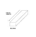
- FIG. 1 is a view showing a rectangular copper strip as a first embodiment of an interconnector material of the present invention.
- FIG. 2 is a diagram showing a first embodiment of the manufacturing method of the present invention.
- FIG. 3 is a view showing a round bar copper as another embodiment of the interconnector material of the present invention.
- FIG. 4 is a diagram showing a second embodiment of the manufacturing method of the present invention.
- the present invention has been developed by paying attention to the relationship between the crystal orientation of the copper alloy material and the Young's modulus.
- the inventor etc. first measured Young's modulus of various crystal orientations using a pure copper single crystal. As a result, it was confirmed that the (111) plane in the plane orthogonal to the rolling direction has a high Young's modulus, and the (100) plane and the (102) plane have a low Young's modulus. Then, the method of controlling the area ratio of the (100) plane, the (102) plane, and the (111) plane in the plane orthogonal to the rolling direction of the solar cell interconnector material was found.
- the interconnector material for a solar cell module of the present invention is made of a copper conductor having an area ratio of (100) plane in a plane orthogonal to the rolling direction of 20 to 90%.
- the copper conductor having a (100) plane area ratio of 20 to 90% in the plane orthogonal to the rolling direction is defined as the (100) plane area ratio of 20% or less in the plane orthogonal to the rolling direction.
- the Young's modulus does not decrease to a desired value, and if it exceeds 90%, the crystal grain size becomes coarse and the fatigue characteristics are deteriorated.
- the area ratio of the (100) plane in the plane orthogonal to the rolling direction is preferably 40 to 90%, more preferably 60 to 90%, from the viewpoint of achieving both Young's modulus and fatigue characteristics.
- the solar cell module interconnector material of the present invention is a copper rectangular wire having a 0.2% proof stress of 150 MPa or less and a Young's modulus of 110 GPa or less. If the 0.2% proof stress is 150 MPa or more, the material strength is too high, so that there is a problem that warpage occurs during solder connection, and it is particularly preferably 130 MPa or less for the reason that warpage during solder connection is reduced. When the Young's modulus is 110 GPa or more, the thermal stress at the time of solder connection is high, and a problem that the cell warps occurs. From the viewpoint of reducing thermal stress, the Young's modulus is preferably 100 GPa or less, particularly 90 GPa or less.
- the solar cell interconnector material of the present invention has a total area ratio of 15 to 95% of the (100) plane and (102) plane in the plane orthogonal to the rolling direction.
- the reason why the total area ratio of the (100) plane and the (102) orientation in the plane orthogonal to the rolling direction is defined as 15 to 95% is to reduce the Young's modulus. 20% or more is particularly preferable for improving both fatigue characteristics and reducing Young's modulus.
- the total area ratio of the (100) plane and the (102) plane in the plane orthogonal to the rolling direction is 15% or less, there is a problem that the cell warps during solder connection, and when it is 95% or more, the fatigue characteristics deteriorate. Because there is.
- the area ratio of the (111) plane in the plane orthogonal to the rolling direction is 10% or less.
- the reason why the ratio is 10% or less is to reduce the Young's modulus. If the ratio is 10% or more, the Young's modulus increases, and there is a problem that the cell is warped during solder connection.
- the solar cell interconnector manufacturing method according to the present invention may be either a method of slitting a thin copper plate to an appropriate width, or a method of rolling a round wire (rough drawing wire) into a round wire or a flat wire.
- the shape of the interconnector material is not particularly limited, but is preferably a rectangular shape from the viewpoint of solder connectivity.
- the “plane perpendicular to the rolling direction” is a plane (that is, a cross section) perpendicular to the longitudinal direction of the interconnector material.
- the solar cell interconnector material according to the present invention is manufactured through a casting step S1, a reheat treatment step S2, a hot rolling step S3, a cold rolling step S4, a heat treatment step S5, and a slit step S6, as shown in FIG. Is done.
- the heat treatment step S5 and the cold rolling step S4 may be repeated a plurality of times so as to obtain a desired texture.
- the manufacturing method of the interconnector material from the round bar illustrated in FIG. 3 includes a casting step S11, a reheat treatment step S12, a hot extrusion step S13, a cold rolling step S14, and a heat treatment step S15, as illustrated in FIG. Do.
- the hot extrusion step S13 the final extrusion is performed at a temperature of 500 ° C. or less until the diameter of the round bar is 8 mm.
- the interconnector material for solar cells of the present invention is manufactured from oxygen-free copper or tough pitch copper.
- the reason for limiting the conductor of the present invention to oxygen-free copper or tough pitch copper is that the power generation efficiency of the solar cell is reduced when the interconnector material has a high resistivity.
- improvement may be achieved by adding some additive elements as appropriate. Whether or not some additive elements are added is determined by comprehensively judging from the electrical conductivity, strength, fatigue characteristics, etc. required by the use environment of the interconnector material.
- Additive elements added to oxygen-free copper or tough pitch copper include Zn, Pb, Fe, Sn, P, and Ag. Addition amounts are: Zn: 0.01 to 1.0 mass%, Pb: 0.01 to 1.0 mass%, Fe: 0.01 to 3.0 mass%, Sn: 0.1 to 3.0 mass% P: 0.001 to 1.0% by mass, Ag: 0.01 to 1.0% by mass, and a combination of one or more elements may be added. By adding such an element, there is an effect that strength and heat resistance are improved. In addition, when it is not necessary to expect the above-mentioned effect, the additive element can be omitted.
- oxygen-free copper or tough pitch copper is cast (FIG. 2, S1), then reheated to 700 to 950 ° C. (FIG. 2, S2), and hot-rolled at a hot rolling end temperature of 500 ° C. or less ( FIG. 2, S3).
- the final pass of the hot rolling process is performed at 500 ° C. or less, so that the crystal grain size after hot rolling is 100 ⁇ m or less.
- the reason why the crystal grain size is 100 ⁇ m or less is to increase the area ratio of the (100) plane and (102) plane in the plane orthogonal to the rolling direction in the recrystallization heat treatment (S5), and after hot rolling
- the crystal grain size exceeds 100 ⁇ m the area of the (100) plane or (102) plane in the plane orthogonal to the rolling direction is reduced in the recrystallization heat treatment, and the (111) plane or (110) plane This is not preferable because it causes a problem that the Young's modulus increases and the Young's modulus increases.
- cold rolling at a rolling rate of 80 to 95% is performed (FIG. 2, S4).
- the rolling rate of one pass during rolling is important. If the rolling rate of one pass is too high, shear deformation is applied, so that the (100) plane and (102) plane in the plane orthogonal to the rolling direction are less likely to develop after heat treatment, and the (111) plane and (110) plane are This is because the rolling texture is likely to increase and the probability of being outside the scope of the present invention increases.
- the rolling rate for one pass is 40% or less, preferably 20% or less.
- the total cold rolling ratio is 80% or more with respect to the copper conductor before the heat treatment.
- the (100) plane and (102) plane in the plane orthogonal to the rolling direction do not grow, and the (111) plane and (110) plane grow easily. It is because it becomes a rolling texture.
- the rolling rate is 95% or more, the (100) plane in the plane orthogonal to the rolling direction grows too much, so that the fatigue characteristics are deteriorated.
- it is also effective to adjust the type and amount of lubricating oil used during rolling or to adjust the rolling speed.
- intermediate annealing may be performed during the cold rolling.
- the total processing rate of cold rolling (S4) before recrystallization heat treatment is 80% or more, and the rolling rate for one pass is 40% or less.
- the heat treatment (S5) after the cold rolling is preferably 200 to 600 ° C. for 5 to 180 minutes. If the heat treatment temperature is too low or the heat treatment time is too short, recrystallization does not occur, the processed structure remains, and the (100) plane and (102) plane in the plane orthogonal to the rolling direction do not grow. When the heat treatment temperature is too high or the heat treatment time is too long, the crystal grains become coarse, and there is a possibility that a crack may occur in the conductor when used as an interconnector material for solar cells.
- the melted oxygen-free copper or tough pitch copper is made into a wire (rough drawing wire) having a diameter of about 8 mm by a belt & wheel method, a twin belt method, an upcast method, or an ingot by a hot extrusion method.
- a round wire of oxygen-free copper or tough pitch copper having a diameter of about 8 mm is drawn to a predetermined diameter, then rolled into a rectangular wire, and then heat treatment with recrystallization is performed. Further, intermediate annealing may be performed during drawing and rolling. The area reduction rate for one pass when drawing is 40% or less.
- the deformation of the drawing process does not become a deformation due to the normal plane strain stress, the deformation due to the shear stress is added, and the drawn texture does not become the desired texture. This is because the (100) plane and (102) plane in the plane perpendicular to the rolling direction of the recrystallized texture do not increase, and the (111) plane and (112) plane increase.
- it is also effective to adjust the type and amount of lubricating oil used during rolling or to adjust the processing speed.
- a round wire is drawn to a predetermined diameter and then rolled to a predetermined thickness to obtain a copper rectangular wire. Since the rolling conditions here are the same as the manufacturing conditions of the slit material, detailed description is omitted, but the rolling rate needs to be in the range of 70 to 95%. The reason why the appropriate rolling ratio differs between the slit material and the round wire rolled material is that the texture before rolling is different between the slit material and the round wire rolled material. In addition, putting intermediate annealing in the middle of rolling is effective for increasing the (100) plane and (102) plane in the plane orthogonal to the rolling direction. However, when performing the intermediate annealing, the heat treatment conditions are preferably 100 to 500 ° C. and 5 to 30 minutes. If the heat treatment temperature is too low, the effect of intermediate annealing cannot be obtained, and if the temperature is too high, the area of the (100) plane or (102) plane in the plane orthogonal to the rolling direction in the subsequent cold rolling or heat treatment Decrease.
- the heat treatment after rolling is desirably 200 to 600 ° C. for 5 to 180 minutes.
- the heat treatment temperature is too low or the heat treatment time is too short, recrystallization does not occur, the processed structure remains, and the (100) plane and the (102) plane do not grow. If the heat treatment temperature is too high or the heat treatment time is too long, the crystal grains become coarse and cracks may occur in the conductor when used as a solar cell interconnector material.
- the area ratio of the (100) plane of the texture of the copper rectangular wire is measured using the SEM-EBSD method (Scanning Electron Microscopic-Electron Back Scattered Diffraction Pattern Method), that is, the electron microscope structure by SEM, using EBSD. be able to.
- SEM-EBSD method Sccanning Electron Microscopic-Electron Back Scattered Diffraction Pattern Method
- a range including 400 or more crystal grains was scanned in 1 ⁇ m steps, and the orientation was analyzed.
- the crystal grains were arbitrarily measured at several points in the plate thickness direction, and the average was obtained. That is, each crystal grain appearing on the SEM screen is irradiated with an electron beam, and each crystal orientation is identified from the diffracted electrons.
- the crystal orientation display method in this specification defines the ratio of the region facing the rolling direction of the material by the area ratio. Calculate the angle between two normal vectors of the (100) and (102) planes of the crystal grains in the measurement region and the rolling direction, and this angle has an atomic plane of less than 10 °.
- the area of a region having an atomic plane in which the angle formed by the (100) plane and the (102) plane and the rolling direction is less than 10 ° is a value obtained by summing the areas with respect to the total measured area. Rate (%).
- the region having a plane is a plane of a rectangular wire that is oriented in the rolling direction of a rectangular wire and whose normal is the rolling direction of a rectangular wire that is an ideal orientation, and a surface itself such as a (100) plane, a (102) plane, a (100) plane, (102 )
- solder layer on the outer periphery of the rectangular wire in consideration of connection with the cell.
- the solder layer is applied by passing a rectangular wire through the molten solder bath.
- solder Sn-based solder can be used.
- the second component include those containing 0.1 mass% or more of Pb, In, Bi, Ag, and Cu.
- Pb-free Sn—Ag, Sn—Ag—Cu, Sn— Cu, Sn—Ag—In, etc. are desirable.
- the copper rectangular wire was made of two types of pure copper, oxygen-free copper and tough pitch copper.
- the production was carried out by two types, a production method of slitting a rolled copper plate and a production method of rolling a round wire.
- Examples 1 to 74 Examples 1 to 37 were cast with oxygen-free copper, and Examples 38 to 74 were cast with tough pitch copper, and then homogenized (reheated) at 900 ° C. for 30 minutes (FIG. 2, S2) to perform hot rolling. (FIG. 2, S3).
- the final pass temperature of the hot rolling was 400 ° C. and 500 ° C. as shown in Table 1 or Table 2.
- water cooling and chamfering were performed to obtain a copper plate having a thickness of 10 mm.
- cold rolling is performed at a rolling rate of 1 pass as shown in Table 1 or 2 at 10 to 40%, and cold rolling with a total cold rolling rate of 80% or more is performed. It was.
- recrystallization heat treatment was performed at 200 ° C., 400 ° C., and 600 ° C. for 30 minutes as shown in Table 1 or Table 2. Thereafter, it was slit into a width of 2 mm, and 20 ⁇ m solder plating was applied to obtain a test material.
- Comparative Examples 1-12 Comparative Examples 1-12 Comparative Examples 1 to 6 were cast oxygen-free copper, and Comparative Examples 7 to 12 were cast tough pitch copper and then subjected to reheating at 900 ° C. for 30 minutes to perform hot rolling, chamfering, cold rolling, and recrystallization heat treatment. It was. The same processing as in Examples 1 to 74 was carried out except that the final pass temperature of hot rolling and the rolling rate of one pass of cold rolling were set to the conditions shown in Table 1 or Table 2, and a 20 ⁇ m solder plated wire was manufactured and served. Samples were used.
- Examples 75-98 In Examples 75 to 86, a round wire made of oxygen-free copper (rough drawing wire) was processed into a flat rectangular wire, and in Examples 87 to 98, a round wire made of tough pitch copper (rough drawing wire) was processed into a flat rectangular wire.
- a round wire having a diameter of 2.6 mm was drawn to a diameter of 0.7 to 1.3 mm.
- the drawing process was performed at a processing rate of 1 pass at 10 to 40% as shown in Tables 3 and 4. Thereafter, cold rolling was performed to obtain a flat wire having a thickness of 0.2 mm. After cold rolling, as shown in Table 3 or Table 4, recrystallization heat treatment was performed at 200 ° C., 400 ° C., and 600 ° C. for 30 minutes, and solder plating with a thickness of 20 ⁇ m was applied to obtain a test material.
- Comparative Examples 13-18 In Comparative Examples 13 to 15, oxygen free copper was processed, and in Comparative Examples 16 to 18, round wires made of tough pitch copper were processed into flat wires. A round wire having a diameter of 2.6 mm was drawn to a diameter of 0.7 mm. The same processing as in Examples 75 to 98 was performed except that the processing rate of one pass of wire drawing processing and the recrystallization heat treatment were changed to the conditions shown in Tables 3 and 4, and a solder plated wire having a thickness of 20 ⁇ m was manufactured and used as a test material. .
- Examples 99-101 In Examples 99 to 101, a round wire made of oxygen-free copper was processed into a flat wire. A round wire having a diameter of 2.6 mm was drawn to a diameter of 0.7 mm. The drawing process was performed at an I-pass processing rate of 10 to 40% as shown in Table 5. Intermediate annealing was performed under the conditions shown in Table 5 during the drawing process. After the wire drawing process, cold rolling was performed to obtain a rectangular wire with a thickness of 0.2 mm, and solder plating with a thickness of 20 ⁇ m was applied to obtain a test material.
- Reference Example 1 and Comparative Example 19 In Reference Example 1 and Comparative Example 19, a round wire made of oxygen-free copper was processed into a flat wire. A round wire with a diameter of 2.6 mm was drawn to a diameter of 0.7 mm, and the processing rate for one pass was processed in the same manner as in Examples 99 to 101 except that the intermediate annealing was performed under the conditions shown in Table 5. A 20 ⁇ m solder plated wire was manufactured and used as a test material.
- the 0.2% proof stress was obtained by taking a JIS Z2201 No. 9 test piece from each specimen and testing it according to JIS Z2241.
- the area ratios of the (100) plane, (102) plane, (110) plane, and (111) plane were measured using a SEM-EBSD method with a scan area of 1,000 ⁇ m ⁇ 1,000 ⁇ m in a scan step of 2 ⁇ m. Measurement was made and the area ratio of each surface was determined to be within 10 °.
- the Young's modulus was obtained by using a test piece having a length of 30 mm by a resonance method.
- the amount of warpage of the solar cell was measured by soldering the produced solder-coated rectangular wire to a silicon plate of 150 mm ⁇ 150 mm and plate thickness: 0.18 mm.
- Table 1 shows the measurement results of Examples 1 to 37 in which a flat wire of oxygen-free copper was formed with a slit.
- Examples 1 to 37 have a low Young's modulus, a small amount of warpage of the solar cell, and good characteristics as an interconnector material.
- Comparative Example 1 since the final temperature of hot rolling was too low, cracking occurred during hot rolling, and production was stopped. Since Comparative Examples 2, 3, and 4 had a hot rolling temperature that was too high, Comparative Example 5 had a cold rolling rate that was too low, and Comparative Example 6 had a recrystallization heat treatment temperature that was too low. ) Surface area ratio decreased and (111) plane area ratio increased, the Young's modulus was outside the range of the present invention, and the amount of warpage of the solar cell increased.
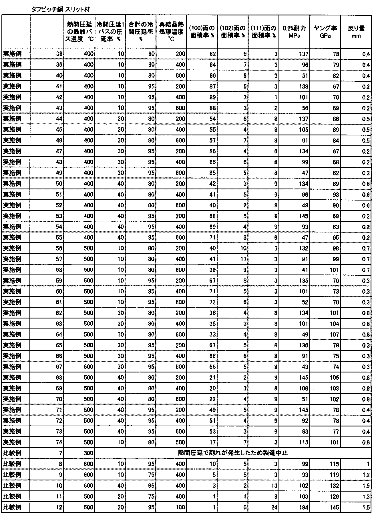
- Table 2 shows the measurement results of Examples 38 to 74 in which a flat wire made of tough pitch copper was formed with slits.
- Examples 38 to 74 have a low Young's modulus, a small amount of warpage of the solar cell, and good characteristics as an interconnector material. On the other hand, since Comparative Example 7 was cracked during hot rolling, production was stopped.
- Comparative Examples 8 to 10 had a hot rolling temperature too high, Comparative Example 11 had a cold rolling rate too low, and Comparative Example 12 had a recrystallization heat treatment temperature too low, so the (100) plane and (102) As the area ratio of the surface decreased, the area ratio of the (111) surface increased, the Young's modulus was outside the range of the present invention, and the amount of warpage of the solar battery cell was increased.
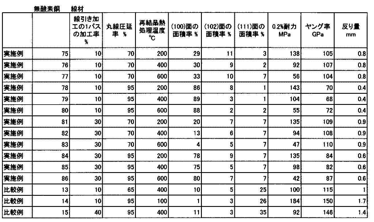
- Table 3 shows the measurement results of Examples 75 to 86 in which a flat wire of oxygen-free copper was prepared from the wire.
- Examples 13 to 18 have a low Young's modulus, a small amount of warpage of the solar cell, and good characteristics as an interconnector material.
- Comparative Example 13 has a drawing rate too low
- Comparative Example 14 has a recrystallization heat treatment temperature too low
- Comparative Example 15 has a drawing rate of one pass that is too high.
- the area ratio of the (102) plane decreased, the area ratio of the (111) plane increased, the Young's modulus was outside the scope of the present invention, and the amount of warpage of the solar battery cell was increased.
- Table 4 shows the measurement results of Examples 87 to 98 in which a flat wire of tough pitch copper was produced from a wire rod.
- Examples 87 to 98 have a low Young's modulus, a small amount of warpage of the solar cell, and good characteristics as an interconnector material.
- Comparative Example 16 has a drawing rate too low
- Comparative Example 17 has a recrystallization heat treatment temperature too low
- Comparative Example 18 has a drawing rate of one pass that is too high.
- the area ratio of the (102) plane decreased, the area ratio of the (111) plane increased, the Young's modulus was outside the scope of the present invention, and the amount of warpage of the solar battery cell was increased.
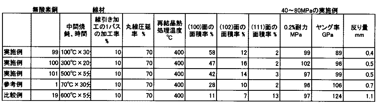
- Table 5 shows the measurement results of Examples 99 to 101 produced in the same manner as Example 76 in Table 3 except that intermediate annealing was performed before final cold rolling.
- Examples 99 to 101 the area ratios of the (100) and (102) planes increased and the amount of warpage of the solar cells decreased compared to Example 76.
- Reference Example 1 since the temperature was too low, the effect of intermediate annealing was not observed, and the amount of warpage was not different from Example 76.
- Comparative Example 19 since the temperature of the intermediate annealing was too high, the crystal grain size after the intermediate annealing became coarse, the area ratios of the (100) plane and the (102) plane after the recrystallization heat treatment decreased, and the Young's modulus was the present invention. Out of the range of the example, the amount of warpage of the solar battery cell was increased.
- the solar cell interconnector material of the present invention is composed of oxygen-free copper and tough pitch copper having a Young's modulus lower than that of a normal copper material. Therefore, thermal stress at the time of soldering can be reduced, and even if the surface of the interconnector material for solar cell is covered with solder and a plurality of silicon cells are connected, cell cracking and warping can be suppressed. It has an excellent effect.
Landscapes
- Photovoltaic Devices (AREA)
- Conductive Materials (AREA)
Abstract
インターコネクタ材のヤング率を低減させ、該コネクタ材でシリコン系セルを接続したときセルの反りの発生を防止すること、また、前記コネクタ材で太陽電池のセルを接合したとき、電池の使用時に発生する熱サイクルでコネクタが破損することのないコネクタを提供する。太陽電池用インターコネクタ材であって、圧延方向に対して直交する面における(100)面の面積率が20~90%、0.2%耐力が150MPa以下、ヤング率が110GPa以下である銅平角線からなる太陽電池用インターコネクタ材である。また、その製造方法は無酸素銅又はタフピッチ銅を鋳造し、再熱し、熱間圧延の終了パス温度を500℃以下として熱間圧延し、次いで80~95%の圧延率の冷間圧延、温度200~600℃で30分の再結晶熱処理し、スリット加工を施し、太陽電池用インターコネクタ材を製造することを特徴とする。
Description
本発明は、複数の太陽電池(セル)からなる太陽電池モジュールにおいて、セル間を接続する配線材として適した太陽電池用インターコネクタ材及びその製造方法に関するものである。
また、本発明は複数のセルからなる太陽電池モジュールにおいて、セル間を接続するのに適した太陽電池用インターコネクタに関するものである。
また、本発明は複数のセルからなる太陽電池モジュールにおいて、セル間を接続するのに適した太陽電池用インターコネクタに関するものである。
近年、太陽電池を利用した発電方式が環境への負荷が少ない方式として着目され、様々な分野で広く利用され、普及が進んでいる。太陽電池モジュールは、シリコン等の半導体の薄板材からなるセルを複数枚配置し、これらのセルが太陽電池用インターコネクタによって電気的に接続された構成となっている。
セル間を電気的に接続するインターコネクタとしては、例えば特許文献1に示すように、無酸素銅やタフピッチ銅からなる銅平角線の外周に半田メッキ層が形成されたものが広く使用されている。この半田メッキ層を介してセルに接続されている。
太陽電池用インターコネクタとセルとの半田付け工程においては、太陽電池用インターコネクタとシリコン系半導体で作られるセルは、半田材を融点以上に昇温して融解させた後、常温にまで冷却する。この時、シリコン系半導体で作られたセルの熱膨張係数と純銅やタフピッチ銅で作られた太陽電池用インターコネクタの熱膨張係数が異なるため、冷却時にセルと太陽電池用インターコネクタとの間に熱応力が生じる。この熱膨張係数の差に基づく熱応力によりセルに反りや割れが発生する問題が生じている。
特に、セルのコストを低減させるために、セルを薄くしたい場合に、この問題は顕著に現れる。
特に、セルのコストを低減させるために、セルを薄くしたい場合に、この問題は顕著に現れる。
この問題を解決するために特許文献1では、導体である純銅の結晶粒を粗大化し、軟質化させることで、接合するセルの半田接合時における反りの低減を図っている。しかし、セルの薄肉化の要求が高くなっており、結晶粒径を粗大化し軟質化させることのみでは、インターコネクタ材の熱応力を低減させることは、困難になりつつある。
また、導体を軟質化させた場合に、その後工程である半田めっき工程、スリット工程、巻き取り工程において、インターコネクタ材が軟らかくなりすぎて線が切れたり、形状が変化したり、長手方向における特性のバラつきが大きくなり、製造歩留まりが低下する課題が指摘されている。このように製造過程での歩留まりが低下するとインターコネクタ材のコストが高くなる問題も生じる。
また、導体を軟質化させた場合に、その後工程である半田めっき工程、スリット工程、巻き取り工程において、インターコネクタ材が軟らかくなりすぎて線が切れたり、形状が変化したり、長手方向における特性のバラつきが大きくなり、製造歩留まりが低下する課題が指摘されている。このように製造過程での歩留まりが低下するとインターコネクタ材のコストが高くなる問題も生じる。
更に、インターコネクタ材が低耐力となり、この低耐力のインターコネクタ材を使用してセル間を接続し太陽電池として使用すると、使用中にインターコネクタ材は熱サイクルによる繰り返し応力を受け、破断しやすくなるといった問題が生じる。
上記理由により、インターコネクタ材の強度を下げずにシリコン系セルの熱膨張係数に近似する熱膨張係数を有するインターコネクタ材が求められている。そして、かかるインターコネクタ材を使用してセル間を接続し、太陽電池としての使用中に熱サイクルを繰り返し受けても、破断するおそれがないインターコネクタが求められている。
上記理由により、インターコネクタ材の強度を下げずにシリコン系セルの熱膨張係数に近似する熱膨張係数を有するインターコネクタ材が求められている。そして、かかるインターコネクタ材を使用してセル間を接続し、太陽電池としての使用中に熱サイクルを繰り返し受けても、破断するおそれがないインターコネクタが求められている。
熱応力は、一般的に次の式で表される。
σ=A×E×α×ΔT
ただし、σは熱応力であり、
Aは面積であり、
Eはヤング率であり、
αは熱膨張係数であり、
ΔTは温度差である。
上式によれば、ヤング率Eを低下させることができれば、熱応力σが比例して減少することが分かる。
σ=A×E×α×ΔT
ただし、σは熱応力であり、
Aは面積であり、
Eはヤング率であり、
αは熱膨張係数であり、
ΔTは温度差である。
上式によれば、ヤング率Eを低下させることができれば、熱応力σが比例して減少することが分かる。
これまでに導体として純銅を用いた太陽電池用インターコネクタ材料において、ヤング率を制御し、熱応力を低減させる、との発想はなされていない。これは従来、ヤング率を低減させることが困難とされてきたためである。本発明者(等)はヤング率を低減させるために種々の検討を行った結果、集合組織の制御により、ヤング率の値を制御することに成功し、本発明に到達した。
なお、塑性加工された多結晶金属はその内部で結晶学的な変化が起きており、それを集合組織の形成という。集合組織とは、金属が圧延や線引きなどの塑性加工を受けると、個々の結晶粒が加工方向に進んで、特定の結晶面だけが規則的に配列することをいう。
太陽電池用インターコネクタ材において集合組織を制御し、材料強度のばらつきを低減した例としては特許文献2が知られている。この特許文献2では圧延方向に対して直交する面における(211)面を制御することで強度のばらつきを低減している。
また、太陽電池用インターコネクタ材において集合組織を制御し、耐力を低減させた例として特許文献3が知られている。特許文献3では、圧延方向に対して直交する面における(114)面、(112)面を制御することで耐力を低減させている。
なお、塑性加工された多結晶金属はその内部で結晶学的な変化が起きており、それを集合組織の形成という。集合組織とは、金属が圧延や線引きなどの塑性加工を受けると、個々の結晶粒が加工方向に進んで、特定の結晶面だけが規則的に配列することをいう。
太陽電池用インターコネクタ材において集合組織を制御し、材料強度のばらつきを低減した例としては特許文献2が知られている。この特許文献2では圧延方向に対して直交する面における(211)面を制御することで強度のばらつきを低減している。
また、太陽電池用インターコネクタ材において集合組織を制御し、耐力を低減させた例として特許文献3が知られている。特許文献3では、圧延方向に対して直交する面における(114)面、(112)面を制御することで耐力を低減させている。
しかしながら特許文献2、3に開示されている技術は、主方位が圧延方向に対して直交する面における(211)面、(114)面、(112)面であり、ヤング率を低下させる方位ではなく、ヤング率については解析していない。
また、これらの特許文献2、3ではX線回折により集合組織を解析している。しかし、X線回折では特定の面方位のみの情報しか得られないため、さまざまな結晶方位粒で構成されている多結晶銅材料については、X線回折では厳密に集合組織を制御することはできていない。
また、これらの特許文献2、3ではX線回折により集合組織を解析している。しかし、X線回折では特定の面方位のみの情報しか得られないため、さまざまな結晶方位粒で構成されている多結晶銅材料については、X線回折では厳密に集合組織を制御することはできていない。
本発明者(等)は、EBSD(Electron Back Scattered Diffraction Pattern)を用いて、集合組織を詳細に解析し、ヤング率を低減させることができる結晶方位粒を集積させる手法を確立し、本発明を完成させるに至った。
本発明は、物理定数であるヤング率に着目し、鋭意検討の結果、インターコネクタ材のヤング率を低減させることで、複数の系セルをインターコネクタ材で半田接続したときの熱応力を減少させ、セルの反りの発生を防止することに成功したものである。
また、本発明はインターコネクタ材で作製したコネクタで太陽電池セルを接合するので、太陽電池の使用時に発生する熱サイクルで破損することのない、インターコネクタを提供することができる。
また、本発明はインターコネクタ材で作製したコネクタで太陽電池セルを接合するので、太陽電池の使用時に発生する熱サイクルで破損することのない、インターコネクタを提供することができる。
好ましくは、本発明の太陽電池モジュールにおいてセル間同士を接続する太陽電池用インターコネクタ材は、圧延方向に対して直交する面における(100)面の面積率が20~90%、0.2%耐力が150MPa以下、ヤング率が110GPa以下の銅平角線である。
さらに好ましくは、本発明の太陽電池モジュールにおいてセル間同士を接続する太陽電池用インターコネクタ材は、圧延方向に対して直交する面における(100)面の面積率が40~90%、0.2%耐力が150MPa以下、ヤング率が100GPa以下の銅平角線である。
また好ましくは、本発明の太陽電池モジュールにおいてセル間同士を接続する太陽電池用インターコネクタ材は、圧延方向に対して直交する面における(100)面の面積率が60~90%、0.2%耐力が150MPa以下、ヤング率が90GPa以下の銅平角線である。
また好ましくは、本発明の太陽電池モジュールにおいてセル間同士を接続する太陽電池用インターコネクタ材は、圧延方向に対して直交する面における(100)面と(102)面の合計の面積率が20~95%、0.2%耐力が150MPa以下、ヤング率が110GPa以下の銅平角線である。
また好ましくは、本発明の太陽電池モジュールにおいてセル間同士を接続する太陽電池用インターコネクタ材は、圧延方向に対して直交する面における(100)面と(102)面の合計の面積率が10~95%、(111)面の面積率が10%以下、0.2%耐力が150MPa以下、ヤング率が110GPa以下の銅平角線である。
本発明の太陽電池用インターコネクタ材の製造方法は、無酸素銅又はタフピッチ銅を鋳造し、再熱し、熱間圧延の終了パス温度を500℃以下として熱間圧延し、次いで80~95%の圧延率の冷間圧延、温度200℃~600℃で30分の再結晶熱処理し、スリット加工を施す製造方法である。該製造方法で、圧延方向に対して直交する面における(100)面の面積率が20~90%、0.2%耐力が150MPa以下、ヤング率が110GPa以下の太陽電池用インターコネクタ材を製造する。
本発明の太陽電池用インターコネクタ材の製造方法は、無酸素銅又はタフピッチ銅を鋳造し、再熱し、熱間圧延の終了パス温度を500℃以下として熱間圧延して熱間圧延後の結晶粒径を100μm以下とし、次いで80~95%の圧延率で冷間圧延し、温度200℃~600℃で30分の再結晶熱処理し、スリット加工を施す製造方法である。該製造方法で、圧延方向に対して直交する面における(100)面の面積率が20~90%、0.2%耐力が130MPa以下、ヤング率が110GPa以下である太陽電池用インターコネクタ材を製造する。
前記太陽電池用インターコネクタ材の製造方法において、前記冷間圧延における1パスの圧延率は40%以下とすることが好ましい。
本発明の太陽電池用インターコネクタ材の製造方法は、無酸素銅又はタフピッチ銅の丸線材を連続鋳造し、伸線加工し、70~95%の丸線圧延を行い平角線とする製造法である。該製造方法で、圧延方向に対して直交する面における(100)面の面積率が20~90%、0.2%耐力が130MPa以下、ヤング率が110GPa以下である銅平角線からなる太陽電池用インターコネクタ材を製造する。
本発明の太陽電池モジュールにおいてセル間同士を接続する太陽電池用インターコネクタは、平角線からなる太陽電池用インターコネクタ材の少なくとも一面に、半田メッキ層が形成されている太陽電池用インターコネクタである。
本発明の太陽電池用インターコネクタ材によれば、通常の純銅系材料と比べてヤング率が低い無酸素銅又はタフピッチ銅で構成されているので、半田接合時の熱応力を低減させることができ、セルの割れや反りを抑制することが可能となる。
本発明は、インターコネクタ材で作成したコネクタで太陽電池セルを接合するので、太陽電池の使用時に発生する熱サイクルでコネクタが破損することがなく、経年使用可能な太陽電池を提供することができる。
本発明は、インターコネクタ材で作成したコネクタで太陽電池セルを接合するので、太陽電池の使用時に発生する熱サイクルでコネクタが破損することがなく、経年使用可能な太陽電池を提供することができる。
本発明は、銅合金材料の結晶方位とヤング率の関係に着目し、開発されたものである。
本発明者(等)は先ず、純銅の単結晶を用いて、さまざまな結晶方位のヤング率を測定した。その結果、圧延方向に対して直交する面における(111)面はヤング率が高く、(100)面と(102)面はヤング率が低いことを確認した。次いで、太陽電池用インターコネクタ材の圧延方向に対して直交する面における(100)面と(102)面および(111)面の面積率を制御する手法を見出した。
本発明者(等)は先ず、純銅の単結晶を用いて、さまざまな結晶方位のヤング率を測定した。その結果、圧延方向に対して直交する面における(111)面はヤング率が高く、(100)面と(102)面はヤング率が低いことを確認した。次いで、太陽電池用インターコネクタ材の圧延方向に対して直交する面における(100)面と(102)面および(111)面の面積率を制御する手法を見出した。
好ましくは、本発明の太陽電池モジュール用インターコネクタ材は、圧延方向に対して直交する面における(100)面の面積率が20~90%の銅導体からなる。
圧延方向に対して直交する面における(100)面の面積率が20~90%の銅導体に規定するのは、圧延方向に対して直交する面における(100)面の面積率が20%以下ではヤング率が所望の値まで減少せず、90%を超えると結晶粒径が粗大になり疲労特性が低下するためである。特に圧延方向に対して直交する面における(100)面の面積率はヤング率と疲労特性の両立の点から40~90%とすることが好ましく、さらに60~90%とすることが特に好ましい。
圧延方向に対して直交する面における(100)面の面積率が20~90%の銅導体に規定するのは、圧延方向に対して直交する面における(100)面の面積率が20%以下ではヤング率が所望の値まで減少せず、90%を超えると結晶粒径が粗大になり疲労特性が低下するためである。特に圧延方向に対して直交する面における(100)面の面積率はヤング率と疲労特性の両立の点から40~90%とすることが好ましく、さらに60~90%とすることが特に好ましい。
また、好ましくは、本発明の太陽電池モジュール用インターコネクタ材は、0.2%耐力が150MPa以下、ヤング率が110GPa以下である銅平角線である。
0.2%耐力が150MPa以上では材料強度が高すぎるため半田接続時に反りが発生する不具合があり、特に半田接続時の反りを減少する、との理由から130MPa以下とすることが好ましい。
ヤング率が110GPa以上では半田接続時の熱応力が高くセルに反りが発生する不具合が生じる。なお、熱応力減少の観点からヤング率は100GPa以下、特には90GPa以下であることが好ましい。
0.2%耐力が150MPa以上では材料強度が高すぎるため半田接続時に反りが発生する不具合があり、特に半田接続時の反りを減少する、との理由から130MPa以下とすることが好ましい。
ヤング率が110GPa以上では半田接続時の熱応力が高くセルに反りが発生する不具合が生じる。なお、熱応力減少の観点からヤング率は100GPa以下、特には90GPa以下であることが好ましい。
本発明の太陽電池用インターコネクタ材は、圧延方向に対して直交する面における(100)面と(102)面の合計の面積率が15~95%、である。圧延方向に対して直交する面における(100)面と(102)方位の合計の面積率を15~95%に規定するのはヤング率を小さくするためで、特に上限を90%以下、下限を20%以上とすることが疲労特性向上とヤング率低減の両立のために特に好ましい。圧延方向に対して直交する面における(100)面と(102)面の合計の面積率が15%以下では半田接続時にセルに反りが生じる不具合があり、95%以上では疲労特性が悪化する不具合があるからである。
また、圧延方向に対して直交する面における(111)面の面積率を10%以下とする。10%以下とするのはヤング率を低下させるためであり、10%以上ではヤング率が大きくなり半田接続時にセルに反りが生じる不具合があるためである。
本発明に係る太陽電池用インターコネクタ材の製造方法は、薄板とした銅板を適宜な幅にスリットする方法か、丸線(荒引き線)を丸線或いは平角線に圧延する方法のどちらでも良い。インターコネクタ材の形状は特に限定する必要はないが、半田接続性の観点から平角形状であることが望ましい。ここで、「圧延方向に対して直交する面」とは、インターコネクタ材の長手方向に垂直な面(すなわち横断面)である。
製造方法に関して、まず図1に図解したスリット材から説明する。
本発明に係る太陽電池用インターコネクタ材は、図2に示すように、鋳造工程S1、再熱処理工程S2、熱間圧延工程S3、冷間圧延工程S4、熱処理工程S5、スリット工程S6を経て製造される。熱処理工程S5と冷間圧延工程S4は所望の集合組織となるように複数回繰り返されても良い。
図3に図解した丸棒からインターコネクタ材の製造方法は、図4に図解のように、鋳造工程S11、再熱処理工程S12、熱間押出工程S13、冷間圧延工程S14、熱処理工程S15、を行う。
熱間押出工程S13において、丸棒の直径8mmまで、最終押出は500℃以下で行う。
本発明に係る太陽電池用インターコネクタ材は、図2に示すように、鋳造工程S1、再熱処理工程S2、熱間圧延工程S3、冷間圧延工程S4、熱処理工程S5、スリット工程S6を経て製造される。熱処理工程S5と冷間圧延工程S4は所望の集合組織となるように複数回繰り返されても良い。
図3に図解した丸棒からインターコネクタ材の製造方法は、図4に図解のように、鋳造工程S11、再熱処理工程S12、熱間押出工程S13、冷間圧延工程S14、熱処理工程S15、を行う。
熱間押出工程S13において、丸棒の直径8mmまで、最終押出は500℃以下で行う。
本発明の太陽電池用インターコネクタ材は、無酸素銅またはタフピッチ銅で製造する。
本発明の導体を無酸素銅又はタフピッチ銅に限定する理由は、インターコネクタ材の抵抗率が高いと太陽電池の発電効率が低下するためである。
インターコネクタ材に無酸素銅やタフピッチ銅と比べて高強度や耐熱性が求められる場合は、適宜若干の添加元素を加えることで改善を図ってもよい。若干の添加元素を加えるか否かはインターコネクタ材の使用環境によって求められる導電率、強度、疲労特性などから総合的に判断して決定する。
本発明の導体を無酸素銅又はタフピッチ銅に限定する理由は、インターコネクタ材の抵抗率が高いと太陽電池の発電効率が低下するためである。
インターコネクタ材に無酸素銅やタフピッチ銅と比べて高強度や耐熱性が求められる場合は、適宜若干の添加元素を加えることで改善を図ってもよい。若干の添加元素を加えるか否かはインターコネクタ材の使用環境によって求められる導電率、強度、疲労特性などから総合的に判断して決定する。
無酸素銅またはタフピッチ銅に加える添加元素は、Zn、Pb、Fe、Sn、P、Agなどがある。添加量はZn:0.01~1.0質量%、Pb:0.01~1.0質量%、Fe:0.01~3.0質量%、Sn:0.1~3.0質量%、P:0.001~1.0質量%、Ag:0.01~1.0質量%の範囲内で一つもしくはそれ以上の元素の組み合わせで添加すればよい。このような元素を添加することで、強度および耐熱性が改善される効果がある。
なお、上記する効果を期待しないで済む場合は添加元素を省略することができる。
なお、上記する効果を期待しないで済む場合は添加元素を省略することができる。
太陽電池用インターコネクタ材としての組織が所望の集合組織となるように、各工程の条件を規定する必要がある。
本発明では無酸素銅またはタフピッチ銅を鋳造(図2、S1)後、700~950℃に再熱(図2、S2)し、熱間圧延の終了温度を500℃以下で熱間圧延する(図2、S3)。
本発明では、熱間圧延工程の最終パスを500℃以下で行うことにより、熱間圧延後の結晶粒径を100μm以下とする。結晶粒径を100μm以下とするのは、再結晶熱処理(S5)において圧延方向に対して直交する面における(100)面や(102)面の面積率を増加させるためであり、熱間圧延後の結晶粒径が100μmを超える場合には、再結晶熱処理において圧延方向に対して直交する面における(100)面や(102)面の面積が減少し、(111)面や(110)面が増加し、ヤング率が高くなる不具合が発生するためで、好ましくない。
本発明では無酸素銅またはタフピッチ銅を鋳造(図2、S1)後、700~950℃に再熱(図2、S2)し、熱間圧延の終了温度を500℃以下で熱間圧延する(図2、S3)。
本発明では、熱間圧延工程の最終パスを500℃以下で行うことにより、熱間圧延後の結晶粒径を100μm以下とする。結晶粒径を100μm以下とするのは、再結晶熱処理(S5)において圧延方向に対して直交する面における(100)面や(102)面の面積率を増加させるためであり、熱間圧延後の結晶粒径が100μmを超える場合には、再結晶熱処理において圧延方向に対して直交する面における(100)面や(102)面の面積が減少し、(111)面や(110)面が増加し、ヤング率が高くなる不具合が発生するためで、好ましくない。
本発明では熱間圧延後、80~95%の圧延率の冷間圧延を施す(図2、S4)。
冷間圧延工程では、圧延時の1パスの圧延率が重要となる。1パスの圧延率が高すぎるとせん断変形が加わるため、熱処理後に圧延方向に対して直交する面における(100)面および(102)面が発達しにくく、(111)面や(110)面が増加しやすい圧延集合組織となり、本発明の範囲外となる確率が高くなるためである。
1パスの圧延率は40%以下とし、好ましくは20%以下とすることが望ましい。
また、熱処理前の銅導体に対して冷間圧延率の合計は80%以上であることが望ましい。80%以下では、熱処理後の再結晶集合組織において、圧延方向に対して直交する面における(100)面および(102)面が成長せず、(111)面や(110)面が成長しやすい圧延集合組織となるためである。なお、圧延率を95%以上とすると圧延方向に対して直交する面における(100)面が成長しすぎるために疲労特性が悪化することになり好ましくない。なお、せん断変形を減少させるために、圧延時に使用する潤滑油の種類や量を調整し、あるいは圧延速度を調整することも有効である。
冷間圧延工程では、圧延時の1パスの圧延率が重要となる。1パスの圧延率が高すぎるとせん断変形が加わるため、熱処理後に圧延方向に対して直交する面における(100)面および(102)面が発達しにくく、(111)面や(110)面が増加しやすい圧延集合組織となり、本発明の範囲外となる確率が高くなるためである。
1パスの圧延率は40%以下とし、好ましくは20%以下とすることが望ましい。
また、熱処理前の銅導体に対して冷間圧延率の合計は80%以上であることが望ましい。80%以下では、熱処理後の再結晶集合組織において、圧延方向に対して直交する面における(100)面および(102)面が成長せず、(111)面や(110)面が成長しやすい圧延集合組織となるためである。なお、圧延率を95%以上とすると圧延方向に対して直交する面における(100)面が成長しすぎるために疲労特性が悪化することになり好ましくない。なお、せん断変形を減少させるために、圧延時に使用する潤滑油の種類や量を調整し、あるいは圧延速度を調整することも有効である。
また、冷間圧延の途中に中間焼鈍を施しても良い。ただし、中間焼鈍を施す場合は、再結晶熱処理前の冷間圧延(S4)の加工率の合計を80%以上とし、1パスの圧延率は40%以下とする。
冷間圧延後の熱処理(S5)は、200~600℃で5分~180分が望ましい。熱処理温度が低すぎ、または熱処理時間が短すぎると、再結晶が生じず、加工組織が残存し、圧延方向に対して直交する面における(100)面および(102)面が成長しない。熱処理温度が高すぎ、または熱処理時間が長すぎる場合は結晶粒が粗大化し、太陽電池用インターコネクタ材として使用したときに導体にクラックが発生するおそれがある。
冷間圧延後の熱処理(S5)は、200~600℃で5分~180分が望ましい。熱処理温度が低すぎ、または熱処理時間が短すぎると、再結晶が生じず、加工組織が残存し、圧延方向に対して直交する面における(100)面および(102)面が成長しない。熱処理温度が高すぎ、または熱処理時間が長すぎる場合は結晶粒が粗大化し、太陽電池用インターコネクタ材として使用したときに導体にクラックが発生するおそれがある。
次に、図3に図解した丸線(荒引き線)から製造する場合を説明する。
溶融した無酸素銅又はタフピッチ銅をベルト&ホイール法、双ベルト法、アップキャスト法で、あるいは鋳塊を熱間押出し法等によって直径約8mmの線材(荒引き線)とする。
直径約8mmの無酸素銅またはタフピッチ銅の丸線を所定の直径まで線引き加工し、その後圧延し平角形状の線材とした後、再結晶を伴う熱処理を実施する。また、線引き途中および圧延途中に中間焼鈍を施しても良い。
線引き加工する際の1パスの減面率は40%以下とする。1パスの減面率が高すぎると、線引き加工の変形が通常の平面ひずみ応力による変形とならず、せん断応力による変形が加わり、線引きの加工集合組織が所望の集合組織とならず、熱処理後の再結晶集合組織が圧延方向に対して直交する面における(100)面および(102)面が増加せず、(111)面や(112)面などが増加するためである。なお、せん断変形を減少させるために、圧延時に使用する潤滑油の種類や量を調整し、あるいは加工速度を調整することも有効である。
溶融した無酸素銅又はタフピッチ銅をベルト&ホイール法、双ベルト法、アップキャスト法で、あるいは鋳塊を熱間押出し法等によって直径約8mmの線材(荒引き線)とする。
直径約8mmの無酸素銅またはタフピッチ銅の丸線を所定の直径まで線引き加工し、その後圧延し平角形状の線材とした後、再結晶を伴う熱処理を実施する。また、線引き途中および圧延途中に中間焼鈍を施しても良い。
線引き加工する際の1パスの減面率は40%以下とする。1パスの減面率が高すぎると、線引き加工の変形が通常の平面ひずみ応力による変形とならず、せん断応力による変形が加わり、線引きの加工集合組織が所望の集合組織とならず、熱処理後の再結晶集合組織が圧延方向に対して直交する面における(100)面および(102)面が増加せず、(111)面や(112)面などが増加するためである。なお、せん断変形を減少させるために、圧延時に使用する潤滑油の種類や量を調整し、あるいは加工速度を調整することも有効である。
丸線を所定の直径まで線引き加工した後、所定の厚さまで圧延し、銅平角線とする。
ここでの圧延条件は前記スリット材の製造条件と同じであるので詳細な説明は省略するが、圧延率を70~95%の範囲内で実施する必要がある。スリット材と丸線圧延材で、適切な圧延率が異なる理由は、圧延前の集合組織がスリット材と丸線圧延材とでは異なるためである。
なお、圧延の途中で中間焼鈍を入れることは、圧延方向に対して直交する面における(100)面や(102)面を増加させることに有効である。ただし、中間焼鈍を施す場合、その熱処理条件は、100~500℃で5~30分とすることが望ましい。熱処理温度が低すぎると中間焼鈍の効果が得られず、温度が高すぎると、その後の冷間圧延、熱処理において圧延方向に対して直交する面における(100)面や(102)面の面積が減少する。
ここでの圧延条件は前記スリット材の製造条件と同じであるので詳細な説明は省略するが、圧延率を70~95%の範囲内で実施する必要がある。スリット材と丸線圧延材で、適切な圧延率が異なる理由は、圧延前の集合組織がスリット材と丸線圧延材とでは異なるためである。
なお、圧延の途中で中間焼鈍を入れることは、圧延方向に対して直交する面における(100)面や(102)面を増加させることに有効である。ただし、中間焼鈍を施す場合、その熱処理条件は、100~500℃で5~30分とすることが望ましい。熱処理温度が低すぎると中間焼鈍の効果が得られず、温度が高すぎると、その後の冷間圧延、熱処理において圧延方向に対して直交する面における(100)面や(102)面の面積が減少する。
圧延後の熱処理は、200~600℃で5分~180分が望ましい。熱処理温度が低すぎる、または熱処理時間が短すぎると、再結晶が生じず、加工組織が残存し、(100)面および(102)面が成長しない。熱処理温度が高すぎる、または熱処理時間が長すぎると、結晶粒が粗大化し、太陽電池用インターコネクタ材として使用したときに導体にクラックが発生する恐れがある。
銅平角線の集合組織の(100)面の面積率の測定は、SEM-EBSD法(Scanning Electron Microscopy-Electron Back Scattered Diffraction Pattern法)、即ち、SEMによる電子顕微鏡組織を、EBSDを用いて測定することができる。
本発明では、結晶粒を400個以上含む範囲を、1μmのステップでスキャンし、方位を解析した。なお、これらの方位分布は板厚方向に変化しているため、板厚方向に何点か任意に結晶粒をとって測定し、その平均をとることによって求めた。
すなわち、SEM画面上にあらわれる個々の結晶粒に電子ビームを照射し、その回折電子から個々の結晶方位を同定する。
本発明では、結晶粒を400個以上含む範囲を、1μmのステップでスキャンし、方位を解析した。なお、これらの方位分布は板厚方向に変化しているため、板厚方向に何点か任意に結晶粒をとって測定し、その平均をとることによって求めた。
すなわち、SEM画面上にあらわれる個々の結晶粒に電子ビームを照射し、その回折電子から個々の結晶方位を同定する。
本明細書における結晶方位の表示方法は、材料の圧延方向に向いている領域の割合を、その面積率で規定したものである。測定領域内の結晶粒の(100)面、(102)面などの面の法線と圧延方向の二つのベクトルのなす角の角度を計算し、この角度が10°未満の原子面を有するものとについて面積を合計し、これを全測定面積で除して得た値を(100)面、(102)面と圧延方向のなす角の角度が10°未満である原子面を有する領域の面積率(%)とした。
すなわち、本発明において、平角線の圧延方向に向く原子面の集積に関し、(100)面、(102)面などの法線と圧延と圧延方向のなす角の角度が10°未満である原子面を有する領域とは、平角線の圧延方向に向く、理想方位である平角線の圧延方向を法線とする(100)面、(102)面などの面自体と、(100)面、(102)面などの面の法線と圧延方向のなす角度の角度が10°未満である原子面のそれぞれとを合わせた領域の合計をいう。
すなわち、本発明において、平角線の圧延方向に向く原子面の集積に関し、(100)面、(102)面などの法線と圧延と圧延方向のなす角の角度が10°未満である原子面を有する領域とは、平角線の圧延方向に向く、理想方位である平角線の圧延方向を法線とする(100)面、(102)面などの面自体と、(100)面、(102)面などの面の法線と圧延方向のなす角度の角度が10°未満である原子面のそれぞれとを合わせた領域の合計をいう。
本発明においてEBSD測定にあたっては、鮮明な菊地線回折像を得るために、機械研磨の後に、コロイダルシリカの砥粒を使用して、基体表面を鏡面研磨した後に、測定を行った。
平角線にセルとの接続を考慮してその外周に半田層を設ける。半田層は溶融した半田浴の中に平角線を通線することによって施す。半田はSn系半田を用いることができる。第2成分としてPb、In、Bi、Ag、Cu、を0.1質量%以上添加するものが挙げられるが、環境汚染防止のためにPbフリーのSn-Ag、Sn-Ag-Cu、Sn-Cu、Sn-Ag-Inなどが望ましい。
以下、実施例に基づき本発明を説明するが、本発明はそれらに限定されるものではない。
本実施例は、銅平角線を無酸素銅とタフピッチ銅の2種類の純銅で作製した。作製は圧延銅板をスリットする製法と丸線を圧延する製法の2種類で実施した。
本実施例は、銅平角線を無酸素銅とタフピッチ銅の2種類の純銅で作製した。作製は圧延銅板をスリットする製法と丸線を圧延する製法の2種類で実施した。
実施例1~74
実施例1~37は無酸素銅を、実施例38~74はタフピッチ銅を鋳造後、900℃で30分の均質化処理(再熱)を施して(図2、S2)熱間圧延を行った(図2、S3)。熱間圧延の最終パス温度は表1又は表2に示すように400℃、500℃で行った。熱間圧延後、水冷、面削を行い、板厚10mmの銅板を得た。その後、1パスの圧延率を表1又は表2に示すように10~40%で冷間圧延を行い、合計の冷間圧延率が80%以上の冷間圧延を行い、板厚0.2mmとした。冷間圧延後、表1又は表2に示すように200℃、400℃、600℃で30分の再結晶熱処理を行った。その後、幅2mmにスリットし、20μmの半田めっきを施し供試材とした。
実施例1~37は無酸素銅を、実施例38~74はタフピッチ銅を鋳造後、900℃で30分の均質化処理(再熱)を施して(図2、S2)熱間圧延を行った(図2、S3)。熱間圧延の最終パス温度は表1又は表2に示すように400℃、500℃で行った。熱間圧延後、水冷、面削を行い、板厚10mmの銅板を得た。その後、1パスの圧延率を表1又は表2に示すように10~40%で冷間圧延を行い、合計の冷間圧延率が80%以上の冷間圧延を行い、板厚0.2mmとした。冷間圧延後、表1又は表2に示すように200℃、400℃、600℃で30分の再結晶熱処理を行った。その後、幅2mmにスリットし、20μmの半田めっきを施し供試材とした。
比較例1~12
比較例1~6は無酸素銅を、比較例7~12はタフピッチ銅を鋳造後、900℃で30分の再熱を施して熱間圧延、面削、冷間圧延、再結晶熱処理を行った。熱間圧延の最終パス温度、冷間圧延の1パスの圧延率を表1又は表2に示す条件とした以外は実施例1~74と同様に加工し、20μmの半田めっき線を製造し供試材とした。
比較例1~6は無酸素銅を、比較例7~12はタフピッチ銅を鋳造後、900℃で30分の再熱を施して熱間圧延、面削、冷間圧延、再結晶熱処理を行った。熱間圧延の最終パス温度、冷間圧延の1パスの圧延率を表1又は表2に示す条件とした以外は実施例1~74と同様に加工し、20μmの半田めっき線を製造し供試材とした。
実施例75~98
実施例75~86は無酸素銅からなる丸線(荒引き線)を平角線に加工し、実施例87~98はタフピッチ銅からなる丸線(荒引き線)を平角線に加工した。
直径2.6mmの丸線を直径0.7~1.3mmまで線引き加工を施した。線引き加工は1パスの加工率を表3、4に示すように10~40%で行った。その後、冷間圧延を行い、板厚0.2mmの平角線とした。冷間圧延後、表3又は表4に示すように200℃、400℃、600℃で30分の再結晶熱処理を行い、厚さ20μmの半田めっきを施し供試材とした。
実施例75~86は無酸素銅からなる丸線(荒引き線)を平角線に加工し、実施例87~98はタフピッチ銅からなる丸線(荒引き線)を平角線に加工した。
直径2.6mmの丸線を直径0.7~1.3mmまで線引き加工を施した。線引き加工は1パスの加工率を表3、4に示すように10~40%で行った。その後、冷間圧延を行い、板厚0.2mmの平角線とした。冷間圧延後、表3又は表4に示すように200℃、400℃、600℃で30分の再結晶熱処理を行い、厚さ20μmの半田めっきを施し供試材とした。
比較例13~18
比較例13~15は無酸素銅を、比較例16~18はタフピッチ銅からなる丸線を平角線に加工した。
直径2.6mmの丸線を直径0.7mmまで線引き加工を施した。線引き加工の1パスの加工率、再結晶熱処理を表3、4に示す条件とした以外は実施例75~98と同じ加工を施し、厚さ20μmの半田めっき線を製造し供試材とした。
比較例13~15は無酸素銅を、比較例16~18はタフピッチ銅からなる丸線を平角線に加工した。
直径2.6mmの丸線を直径0.7mmまで線引き加工を施した。線引き加工の1パスの加工率、再結晶熱処理を表3、4に示す条件とした以外は実施例75~98と同じ加工を施し、厚さ20μmの半田めっき線を製造し供試材とした。
実施例99~101
実施例99~101は無酸素銅からなる丸線を平角線に加工した。
直径2.6mmの丸線を直径0.7mmまで線引き加工を施した。線引き加工はIパスの加工率を表5に示すように10~40%で行った。この線引き加工の途中で表5に示す条件で中間焼鈍を行った。線引き加工後、冷間圧延を行い、板厚0.2mmの平角線とし、厚さ20μmの半田めっきを施し供試材とした。
実施例99~101は無酸素銅からなる丸線を平角線に加工した。
直径2.6mmの丸線を直径0.7mmまで線引き加工を施した。線引き加工はIパスの加工率を表5に示すように10~40%で行った。この線引き加工の途中で表5に示す条件で中間焼鈍を行った。線引き加工後、冷間圧延を行い、板厚0.2mmの平角線とし、厚さ20μmの半田めっきを施し供試材とした。
参考例1,比較例19
参考例1、比較例19は無酸素銅をからなる丸線を平角線に加工した。
直径2.6mmの丸線を直径0.7mmまで線引き加工を施し、1パスの加工率を、中間焼鈍を表5に示す条件とした以外は実施例99~101と同様に加工し、厚さ20μmの半田めっき線を製造し供試材とした。
参考例1、比較例19は無酸素銅をからなる丸線を平角線に加工した。
直径2.6mmの丸線を直径0.7mmまで線引き加工を施し、1パスの加工率を、中間焼鈍を表5に示す条件とした以外は実施例99~101と同様に加工し、厚さ20μmの半田めっき線を製造し供試材とした。


評価項目として以下をそれぞれ評価した。
(1)0.2%耐力、
(2)(100)面、(102)面、(110)面、(111)面の面積率、
(3)ヤング率
(4)太陽電池の反り量
(1)0.2%耐力、
(2)(100)面、(102)面、(110)面、(111)面の面積率、
(3)ヤング率
(4)太陽電池の反り量
(1)0.2%耐力は、各供試材からJIS Z2201の9号試験片を採取し、JIS Z2241に準拠して試験した。
(2)(100)面、(102)面、(110)面、(111)面の面積率は、SEM-EBSD法を用いて測定面積1,000μm×1,000μmの領域をスキャンステップ2μmで測定し、各面のずれ角度10°以内のものを各面の面積率として求めた。
(3)ヤング率は、共振法により長さ30mmの試験片を用いて求めた。
(4)太陽電池の反り量は、150mm×150mm、板厚:0.18mmのシリコン板に、作製した半田被覆平角線を半田接続した際の反り量を測定した。
(2)(100)面、(102)面、(110)面、(111)面の面積率は、SEM-EBSD法を用いて測定面積1,000μm×1,000μmの領域をスキャンステップ2μmで測定し、各面のずれ角度10°以内のものを各面の面積率として求めた。
(3)ヤング率は、共振法により長さ30mmの試験片を用いて求めた。
(4)太陽電池の反り量は、150mm×150mm、板厚:0.18mmのシリコン板に、作製した半田被覆平角線を半田接続した際の反り量を測定した。
無酸素銅の平角線をスリットで作製した実施例1~37の測定結果を表1に示す。
実施例1~37はヤング率が低く、太陽電池の反り量が小さくインターコネクタ材として良好な特性を示している。
一方、比較例1は、熱間圧延の最終温度が低すぎたため熱間圧延中に割れが生じ、製造を中止した。比較例2、3、4は熱間圧延温度が高すぎたため、比較例5は冷間圧延率が低すぎたため、比較例6は再結晶熱処理温度が低すぎたため、(100)面や(102)面の面積率が減少するとともに(111)面の面積率が増加し、ヤング率が本発明の範囲外となり、太陽電池セルの反り量が大きくなった。
実施例1~37はヤング率が低く、太陽電池の反り量が小さくインターコネクタ材として良好な特性を示している。
一方、比較例1は、熱間圧延の最終温度が低すぎたため熱間圧延中に割れが生じ、製造を中止した。比較例2、3、4は熱間圧延温度が高すぎたため、比較例5は冷間圧延率が低すぎたため、比較例6は再結晶熱処理温度が低すぎたため、(100)面や(102)面の面積率が減少するとともに(111)面の面積率が増加し、ヤング率が本発明の範囲外となり、太陽電池セルの反り量が大きくなった。
タフピッチ銅の平角線をスリットで作製した実施例38~74の測定結果を表2に示す。
実施例38~74はヤング率が低く、太陽電池の反り量が小さくインターコネクタ材として良好な特性を示している。
一方、比較例7は熱間圧延の途中で割れが発生したため、製造を中止した。比較例8~10は熱間圧延の温度が高すぎたため、比較例11は冷間圧延率が低すぎたため、比較例12は再結晶熱処理温度が低すぎたため、(100)面や(102)面の面積率が減少するとともに(111)面の面積率が増加し、ヤング率が本発明の範囲外となり、太陽電池セルの反り量が大きくなった。
実施例38~74はヤング率が低く、太陽電池の反り量が小さくインターコネクタ材として良好な特性を示している。
一方、比較例7は熱間圧延の途中で割れが発生したため、製造を中止した。比較例8~10は熱間圧延の温度が高すぎたため、比較例11は冷間圧延率が低すぎたため、比較例12は再結晶熱処理温度が低すぎたため、(100)面や(102)面の面積率が減少するとともに(111)面の面積率が増加し、ヤング率が本発明の範囲外となり、太陽電池セルの反り量が大きくなった。
無酸素銅の平角線を線材から作製した実施例75~86の測定結果を表3に示す。実施例13~18はヤング率が低く、太陽電池の反り量が小さくインターコネクタ材として良好な特性を示している。
一方、比較例13は線引き加工率が低すぎるため、比較例14は再結晶熱処理温度が低すぎるため、比較例15は線引き加工率の1パスの加工率が高すぎるため、(100)面や(102)面の面積率が減少するとともに(111)面の面積率が増加し、ヤング率が本発明の範囲外となり、太陽電池セルの反り量が大きくなった。
一方、比較例13は線引き加工率が低すぎるため、比較例14は再結晶熱処理温度が低すぎるため、比較例15は線引き加工率の1パスの加工率が高すぎるため、(100)面や(102)面の面積率が減少するとともに(111)面の面積率が増加し、ヤング率が本発明の範囲外となり、太陽電池セルの反り量が大きくなった。
タフピッチ銅の平角線を線材から作製した実施例87~98の測定結果を表4に示す。実施例87~98はヤング率が低く、太陽電池の反り量が小さくインターコネクタ材として良好な特性を示している。
一方、比較例16は線引き加工率が低すぎるため、比較例17は再結晶熱処理温度が低すぎるため、比較例18は線引き加工率の1パスの加工率が高すぎるため、(100)面や(102)面の面積率が減少するとともに(111)面の面積率が増加し、ヤング率が本発明の範囲外となり、太陽電池セルの反り量が大きくなった。
一方、比較例16は線引き加工率が低すぎるため、比較例17は再結晶熱処理温度が低すぎるため、比較例18は線引き加工率の1パスの加工率が高すぎるため、(100)面や(102)面の面積率が減少するとともに(111)面の面積率が増加し、ヤング率が本発明の範囲外となり、太陽電池セルの反り量が大きくなった。
最終冷間圧延前に中間焼鈍を施した以外は表3の実施例76と同様に作製した実施例99~101の測定結果を表5に示す。実施例99~101は、実施例76と比べて、(100)及び(102)面の面積率が上昇し、さらに太陽電池セルの反り量が減少した。
参考例1は、温度が低すぎるため中間焼鈍の効果が見られず反り量は実施例76と変わらなかった。
比較例19は中間焼鈍の温度が高すぎたため、中間焼鈍後の結晶粒径が粗大化し、再結晶熱処理後の(100)面及び(102)面の面積率が減少し、ヤング率が本発明例の範囲外となり、太陽電池セルの反り量が大きくなった。
参考例1は、温度が低すぎるため中間焼鈍の効果が見られず反り量は実施例76と変わらなかった。
比較例19は中間焼鈍の温度が高すぎたため、中間焼鈍後の結晶粒径が粗大化し、再結晶熱処理後の(100)面及び(102)面の面積率が減少し、ヤング率が本発明例の範囲外となり、太陽電池セルの反り量が大きくなった。
以上詳述したように、本発明の太陽電池用インターコネクタ材は、通常の銅材料と比べてヤング率が低い無酸素銅及びタフピッチ銅で構成されている。従って、半田接合時の熱応力を低減させることができ、この太陽電池用インターコネクタ材表面を半田で被覆し、複数のシリコンセルを接続しても、セルの割れや反りを抑制することができる優れた効果を有するものである。
Claims (10)
- 太陽電池モジュールにおいてセル間同士を接続する太陽電池用インターコネクタ材であって、圧延方向に対して直交する面における(100)面の面積率が20~90%、0.2%耐力が150MPa以下、ヤング率が110GPa以下である銅平角線からなる太陽電池用インターコネクタ材。
- 請求項1において、圧延方向に対して直交する面における(100)面の面積率が40~90%、0.2%耐力が150MPa以下、ヤング率が100GPa以下である銅平角線からなる太陽電池用インターコネクタ材。
- 請求項1において、圧延方向に対して直交する面における(100)面の面積率が60~90%、0.2%耐力が150MPa以下、ヤング率が90GPa以下である銅平角線からなる太陽電池用インターコネクタ材。
- 太陽電池モジュールにおいてセル間同士を接続する太陽電池用インターコネクタ材であって、圧延方向に対して直交する面における(100)面と(102)面の合計の面積率が20~95%、0.2%耐力が150MPa以下、ヤング率が110GPa以下である銅平角線からなる太陽電池用インターコネクタ材。
- 太陽電池モジュールにおいてセル間同士を接続する太陽電池用インターコネクタ材であって、圧延方向に対して直交する面における(100)面と(102)面の合計の面積率が10~95%、(111)面の面積率が10%以下、0.2%耐力が150MPa以下、ヤング率が110GPa以下である銅平角線からなる太陽電池用インターコネクタ材。
- 無酸素銅又はタフピッチ銅を鋳造し、再熱し、熱間圧延の終了パス温度を500℃以下として熱間圧延し、次いで80~95%の圧延率の冷間圧延、温度200~600℃で30分の再結晶熱処理し、スリット加工を施し、圧延方向に対して直交する面における(100)面の面積率が20~90%、0.2%耐力が150MPa以下、ヤング率が110GPa以下の太陽電池用インターコネクタ材を製造することを特徴とする太陽電池用インターコネクタ材の製造方法。
- 請求項6において、前記熱間圧延後の結晶粒径を100μm以下とし、0.2%耐力が130MPa以下である太陽電池用インターコネクタ材を製造することを特徴とする太陽電池用インターコネクタ材の製造方法。
- 請求項6又は7において、前記冷間圧延における1パスの圧延率が40%以下である太陽電池用インターコネクタ材の製造方法。
- 無酸素銅又はタフピッチ銅の丸線材を連続鋳造し、伸線加工し、70~95%の丸線圧延を行い平角線とし、圧延方向に対して直交する面における(100)面の面積率が20~90%、0.2%耐力が130MPa以下、ヤング率が110GPa以下である銅平角線からなる太陽電池用インターコネクタ材を製造することを特徴とする太陽電池用インターコネクタ材の製造方法。
- 太陽電池モジュールにおいてセル間同士を接続する太陽電池用インターコネクタであって、請求項1~請求項5のいずれかに記載の平角線からなる太陽電池用インターコネクタ材の少なくとも一面に、半田メッキ層が形成されていることを特徴とする太陽電池用インターコネクタ。
Priority Applications (1)
| Application Number | Priority Date | Filing Date | Title |
|---|---|---|---|
| JP2011546496A JP5261579B2 (ja) | 2010-08-04 | 2011-08-04 | 太陽電池用インターコネクタ材、その製造方法及び太陽電池用インターコネクタ |
Applications Claiming Priority (2)
| Application Number | Priority Date | Filing Date | Title |
|---|---|---|---|
| JP2010175137 | 2010-08-04 | ||
| JP2010-175137 | 2010-08-04 |
Publications (1)
| Publication Number | Publication Date |
|---|---|
| WO2012018079A1 true WO2012018079A1 (ja) | 2012-02-09 |
Family
ID=45559575
Family Applications (1)
| Application Number | Title | Priority Date | Filing Date |
|---|---|---|---|
| PCT/JP2011/067860 Ceased WO2012018079A1 (ja) | 2010-08-04 | 2011-08-04 | 太陽電池用インターコネクタ材、その製造方法及び太陽電池用インターコネクタ |
Country Status (3)
| Country | Link |
|---|---|
| JP (1) | JP5261579B2 (ja) |
| TW (1) | TW201214728A (ja) |
| WO (1) | WO2012018079A1 (ja) |
Citations (3)
| Publication number | Priority date | Publication date | Assignee | Title |
|---|---|---|---|---|
| JP2010073445A (ja) * | 2008-09-17 | 2010-04-02 | Nippon Steel Corp | 電気導体及びその製造方法並びに集電用インターコネクター |
| JP2010141050A (ja) * | 2008-12-10 | 2010-06-24 | Hitachi Cable Ltd | 太陽電池用リード線およびその製造方法 |
| WO2010079707A1 (ja) * | 2009-01-09 | 2010-07-15 | 三菱伸銅株式会社 | 高強度高導電銅合金圧延板及びその製造方法 |
-
2011
- 2011-08-04 TW TW100127888A patent/TW201214728A/zh unknown
- 2011-08-04 WO PCT/JP2011/067860 patent/WO2012018079A1/ja not_active Ceased
- 2011-08-04 JP JP2011546496A patent/JP5261579B2/ja not_active Expired - Fee Related
Patent Citations (3)
| Publication number | Priority date | Publication date | Assignee | Title |
|---|---|---|---|---|
| JP2010073445A (ja) * | 2008-09-17 | 2010-04-02 | Nippon Steel Corp | 電気導体及びその製造方法並びに集電用インターコネクター |
| JP2010141050A (ja) * | 2008-12-10 | 2010-06-24 | Hitachi Cable Ltd | 太陽電池用リード線およびその製造方法 |
| WO2010079707A1 (ja) * | 2009-01-09 | 2010-07-15 | 三菱伸銅株式会社 | 高強度高導電銅合金圧延板及びその製造方法 |
Also Published As
| Publication number | Publication date |
|---|---|
| JP5261579B2 (ja) | 2013-08-14 |
| TW201214728A (en) | 2012-04-01 |
| JPWO2012018079A1 (ja) | 2013-10-03 |
Similar Documents
| Publication | Publication Date | Title |
|---|---|---|
| KR101223697B1 (ko) | 금속 테이프 재료 및 태양전지 집전용 인터커넥터 | |
| JP5448763B2 (ja) | 銅合金材料 | |
| JP5077416B2 (ja) | 軟質希薄銅合金材料、軟質希薄銅合金線、軟質希薄銅合金板、軟質希薄銅合金撚線およびこれらを用いたケーブル、同軸ケーブルおよび複合ケーブル | |
| JP4780008B2 (ja) | 太陽電池用めっき線及びその製造方法 | |
| JP6719316B2 (ja) | 放熱部材用銅合金板材およびその製造方法 | |
| KR20190134455A (ko) | 구리판 부착 절연 기판용 구리판재 및 그 제조 방법 | |
| JP5451674B2 (ja) | 電子材料用Cu−Si−Co系銅合金及びその製造方法 | |
| JP5041455B2 (ja) | 太陽電池用リード線及びその製造方法 | |
| KR20110031987A (ko) | 고강도 고도전 동합금 압연판 및 그 제조 방법 | |
| WO2012132937A1 (ja) | 電子材料用Cu-Co-Si系銅合金条及びその製造方法 | |
| TW201303048A (zh) | 銅合金板材及其製造方法 | |
| JP5499330B2 (ja) | 太陽電池用バスバー | |
| WO2016002770A1 (ja) | 金属線、太陽電池集電用インターコネクター、太陽電池モジュール、及び金属線の製造方法 | |
| JP2013049893A (ja) | 太陽電池インターコネクタ用導体及び太陽電池用インターコネクタ | |
| KR101317566B1 (ko) | 동합금 열간단조품 및 동합금 열간단조품의 제조 방법 | |
| JP5261579B2 (ja) | 太陽電池用インターコネクタ材、その製造方法及び太陽電池用インターコネクタ | |
| JP2011021225A (ja) | 端子・コネクタ用銅合金材及びその製造方法 | |
| WO2023106241A1 (ja) | 銅系線材および半導体デバイス | |
| JP4617884B2 (ja) | 接続用リード線およびその製造方法 | |
| JP2014509444A (ja) | 光起電モジュール内においてシリコンウエハを装着するための新しい導体 | |
| JP5088449B2 (ja) | 軟質希薄銅合金材料、軟質希薄銅合金線、軟質希薄銅合金板、軟質希薄銅合金撚線およびこれらを用いたケーブル | |
| JP5565262B2 (ja) | 加工性に優れたクラッド材及びその製造方法 | |
| JP5741849B2 (ja) | 太陽電池インターコネクタ用導体及び太陽電池用インターコネクタ | |
| JP2013040384A (ja) | 軟質希薄銅合金を用いた配線材及び板材 | |
| JP5981087B2 (ja) | 平角銅線及びその製造方法、並びに太陽電池用平角銅線及びその製造方法 |
Legal Events
| Date | Code | Title | Description |
|---|---|---|---|
| WWE | Wipo information: entry into national phase |
Ref document number: 2011546496 Country of ref document: JP |
|
| 121 | Ep: the epo has been informed by wipo that ep was designated in this application |
Ref document number: 11814704 Country of ref document: EP Kind code of ref document: A1 |
|
| NENP | Non-entry into the national phase |
Ref country code: DE |
|
| 122 | Ep: pct application non-entry in european phase |
Ref document number: 11814704 Country of ref document: EP Kind code of ref document: A1 |