WO2012014477A1 - 有機el表示装置 - Google Patents
有機el表示装置 Download PDFInfo
- Publication number
- WO2012014477A1 WO2012014477A1 PCT/JP2011/004274 JP2011004274W WO2012014477A1 WO 2012014477 A1 WO2012014477 A1 WO 2012014477A1 JP 2011004274 W JP2011004274 W JP 2011004274W WO 2012014477 A1 WO2012014477 A1 WO 2012014477A1
- Authority
- WO
- WIPO (PCT)
- Prior art keywords
- voltage
- power supply
- feedback circuit
- unit
- bus wiring
- Prior art date
- Legal status (The legal status is an assumption and is not a legal conclusion. Google has not performed a legal analysis and makes no representation as to the accuracy of the status listed.)
- Ceased
Links
Images









Classifications
-
- G—PHYSICS
- G09—EDUCATION; CRYPTOGRAPHY; DISPLAY; ADVERTISING; SEALS
- G09G—ARRANGEMENTS OR CIRCUITS FOR CONTROL OF INDICATING DEVICES USING STATIC MEANS TO PRESENT VARIABLE INFORMATION
- G09G3/00—Control arrangements or circuits, of interest only in connection with visual indicators other than cathode-ray tubes
- G09G3/20—Control arrangements or circuits, of interest only in connection with visual indicators other than cathode-ray tubes for presentation of an assembly of a number of characters, e.g. a page, by composing the assembly by combination of individual elements arranged in a matrix no fixed position being assigned to or needed to be assigned to the individual characters or partial characters
- G09G3/22—Control arrangements or circuits, of interest only in connection with visual indicators other than cathode-ray tubes for presentation of an assembly of a number of characters, e.g. a page, by composing the assembly by combination of individual elements arranged in a matrix no fixed position being assigned to or needed to be assigned to the individual characters or partial characters using controlled light sources
- G09G3/30—Control arrangements or circuits, of interest only in connection with visual indicators other than cathode-ray tubes for presentation of an assembly of a number of characters, e.g. a page, by composing the assembly by combination of individual elements arranged in a matrix no fixed position being assigned to or needed to be assigned to the individual characters or partial characters using controlled light sources using electroluminescent panels
-
- G—PHYSICS
- G09—EDUCATION; CRYPTOGRAPHY; DISPLAY; ADVERTISING; SEALS
- G09G—ARRANGEMENTS OR CIRCUITS FOR CONTROL OF INDICATING DEVICES USING STATIC MEANS TO PRESENT VARIABLE INFORMATION
- G09G3/00—Control arrangements or circuits, of interest only in connection with visual indicators other than cathode-ray tubes
- G09G3/20—Control arrangements or circuits, of interest only in connection with visual indicators other than cathode-ray tubes for presentation of an assembly of a number of characters, e.g. a page, by composing the assembly by combination of individual elements arranged in a matrix no fixed position being assigned to or needed to be assigned to the individual characters or partial characters
- G09G3/22—Control arrangements or circuits, of interest only in connection with visual indicators other than cathode-ray tubes for presentation of an assembly of a number of characters, e.g. a page, by composing the assembly by combination of individual elements arranged in a matrix no fixed position being assigned to or needed to be assigned to the individual characters or partial characters using controlled light sources
- G09G3/30—Control arrangements or circuits, of interest only in connection with visual indicators other than cathode-ray tubes for presentation of an assembly of a number of characters, e.g. a page, by composing the assembly by combination of individual elements arranged in a matrix no fixed position being assigned to or needed to be assigned to the individual characters or partial characters using controlled light sources using electroluminescent panels
- G09G3/32—Control arrangements or circuits, of interest only in connection with visual indicators other than cathode-ray tubes for presentation of an assembly of a number of characters, e.g. a page, by composing the assembly by combination of individual elements arranged in a matrix no fixed position being assigned to or needed to be assigned to the individual characters or partial characters using controlled light sources using electroluminescent panels semiconductive, e.g. using light-emitting diodes [LED]
- G09G3/3208—Control arrangements or circuits, of interest only in connection with visual indicators other than cathode-ray tubes for presentation of an assembly of a number of characters, e.g. a page, by composing the assembly by combination of individual elements arranged in a matrix no fixed position being assigned to or needed to be assigned to the individual characters or partial characters using controlled light sources using electroluminescent panels semiconductive, e.g. using light-emitting diodes [LED] organic, e.g. using organic light-emitting diodes [OLED]
- G09G3/3225—Control arrangements or circuits, of interest only in connection with visual indicators other than cathode-ray tubes for presentation of an assembly of a number of characters, e.g. a page, by composing the assembly by combination of individual elements arranged in a matrix no fixed position being assigned to or needed to be assigned to the individual characters or partial characters using controlled light sources using electroluminescent panels semiconductive, e.g. using light-emitting diodes [LED] organic, e.g. using organic light-emitting diodes [OLED] using an active matrix
- G09G3/3233—Control arrangements or circuits, of interest only in connection with visual indicators other than cathode-ray tubes for presentation of an assembly of a number of characters, e.g. a page, by composing the assembly by combination of individual elements arranged in a matrix no fixed position being assigned to or needed to be assigned to the individual characters or partial characters using controlled light sources using electroluminescent panels semiconductive, e.g. using light-emitting diodes [LED] organic, e.g. using organic light-emitting diodes [OLED] using an active matrix with pixel circuitry controlling the current through the light-emitting element
-
- G—PHYSICS
- G09—EDUCATION; CRYPTOGRAPHY; DISPLAY; ADVERTISING; SEALS
- G09G—ARRANGEMENTS OR CIRCUITS FOR CONTROL OF INDICATING DEVICES USING STATIC MEANS TO PRESENT VARIABLE INFORMATION
- G09G2330/00—Aspects of power supply; Aspects of display protection and defect management
- G09G2330/02—Details of power systems and of start or stop of display operation
- G09G2330/028—Generation of voltages supplied to electrode drivers in a matrix display other than LCD
Definitions
- the present invention relates to an organic EL (Electro Luminescence) display device, and more particularly to a technique for improving display quality in an organic EL display device.
- organic EL Electro Luminescence
- An organic EL display device is known as a thin and light-emitting display device capable of obtaining self-luminescence having high-speed response and a wide viewing angle by utilizing an electroluminescence phenomenon of an organic compound.
- the organic EL display device includes a display unit in which a large number of pixel units that are individually controlled to emit light are arranged in a plane, and a control unit that controls light emission of the pixel units.
- a pixel current for causing each pixel portion in the display portion to emit light is supplied through a power supply bus wiring (also simply referred to as a bus wiring) provided on the outer periphery of the display portion.
- each power supply line and the power supply are connected to each other with a suitable length of wiring.
- the wiring resistance from the power supply to each power supply line is configured to be equal.
- the voltage drop of each power supply line becomes uniform, and the light emission luminance becomes uniform.
- two sub voltage pads are arranged opposite to each other on both sides of the display unit, and the two sub electrode pads are connected to each other by a low resistance connecting unit. Configured. In such a display device, the voltages of the two sub voltage pads are made uniform, so that the luminance of the entire screen can be made uniform.
- the voltage non-uniformity generated in the bus wiring is, for example, when the organic EL display device is increased in size and narrowed and the bus wiring having a sufficiently low resistance (large area) with respect to the required pixel current cannot be provided. Is particularly noticeable.
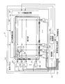
- FIG. 19 is a diagram illustrating a conventional problem using an example of a general organic EL display device 9.
- the organic EL display device 9 includes a display panel 19, a panel control unit 50, a power supply unit 60, and wiring 61.
- the display panel 19 includes a display unit 20, a bus line 21, a signal line driving circuit 40, and a gate line driving circuit 42.
- a bus wiring 21 is provided on the outer peripheral portion of the display unit 20, and the bus wiring 21 is connected to the power supply unit 60 through the wiring 61 at the plurality of connection units 22.
- a pixel current is supplied by a wiring extending from each connection portion 22 of the bus wiring 21 to the inside of the display unit 20.
- the panel control unit 50 receives a video signal representing an image to be displayed on the organic EL display device 9 from the outside of the organic EL display device 9, and the signal line driving circuit 40 and the gate line driving circuit according to the video signal. 42 is controlled.
- Each pixel unit in the display unit 20 has individual luminance by using the pixel current supplied from each connection unit 22 of the bus wiring 21 according to control from the signal line driving circuit 40 and the gate line driving circuit 42. Emits light. Thereby, the video represented by the video signal is displayed on the display unit 20.
- the resistance of the bus wiring 21 and the wiring 61 is shown. These resistors actually include the resistance of the wiring formed on the display panel 19 and the resistance of the wiring of the flexible substrate attached to the display panel 19.
- FIG. 19 it is considered to display an image in which an area in the lower left corner of the drawing has high luminance (for example, white) and another area has uniform low luminance (for example, uniform gray). .
- a larger amount of pixel current flows in the pixel portion located in the high luminance region than in the other pixel portions, and the magnitude of the pixel current is biased in the display surface.
- Such non-uniform pixel current forms a complex voltage distribution on the circuit network constituted by the resistance of the bus wiring 21 and the wiring 61.
- the voltages V x1 , V y1 As a result, the voltages V x1 , V y1 .
- the bus wiring 21 supplies positive power
- the voltage of the connection portion 22 located near the high luminance region is lower than the voltage of the other connection portions 22.
- the luminance of the pixel portion (more precisely, the pixel current determined from the operating point of the drive transistor included in the pixel portion) becomes non-uniform, The quality of the displayed video deteriorates. Specifically, as shown in FIG. 19, luminance unevenness occurs such that an area to be displayed in uniform gray is dark in the vicinity of the white area and becomes brighter as the distance from the white area increases.
- the present invention has been made in view of the above circumstances, and an organic current in which a pixel current for causing each pixel unit in the display unit to emit light is supplied through a bus line that is a power supply line provided on the outer periphery of the display unit.
- An object of the present invention is to provide an organic EL display device having a suitable configuration for reducing deterioration in display quality caused by non-uniform voltage generated in bus wiring.
- one aspect of the organic EL display device includes a display unit in which a plurality of pixel units including organic EL elements are arranged on a substrate, an outer periphery of the display unit, A power supply bus line for supplying a drive voltage for driving each pixel part included in the display part to each pixel part; a feedback circuit part for generating an output voltage and supplying the output voltage to the power supply bus line; and the feedback circuit part.
- a power supply unit that supplies a power supply voltage composed of a high power supply voltage for driving and a low power supply voltage lower than the high power supply voltage to the feedback circuit unit, and a target voltage applied to the voltage of the power supply bus line are defined
- a reference voltage generation unit that supplies a reference voltage to the feedback circuit unit, wherein the feedback circuit unit generates the output voltage based on a power supply voltage supplied from the power supply unit, and the feedback circuit unit includes: Before the power supply voltage A first power supply terminal to which a high power supply voltage is applied; a second power supply terminal to which the low power supply voltage is applied among the power supply voltages; a first input terminal to which the reference voltage is applied; An output terminal connected to a connection part which is a part, a second input terminal to which a voltage at the connection part of the power supply bus wiring is applied, the first power supply terminal, the second power supply terminal, the first An input terminal, a switching control circuit connected to the second input terminal, one terminal connected to one of the first power supply terminal and the second power supply terminal, and the
- the difference that is output to and added is the resistance between the output terminal of the feedback circuit unit and the connection part of the power supply bus line, and the connection part of the output terminal of the feedback circuit part and the power supply bus line. Corresponds to the amount of voltage drop determined by the product of the current flowing between and.
- the bus wiring is arranged along the edge of the display unit, the plurality of feedback circuit units are arranged outside the display unit, the feedback circuit unit generates an output voltage, and the generated output voltage is transmitted to the bus wiring. And a voltage at the connection portion is monitored. A reference voltage is applied to the feedback circuit unit, and the feedback circuit unit adjusts the output voltage so that the monitored voltage is equal to the target voltage defined by the applied reference voltage. The voltage becomes uniform regardless of the display pattern, and the display quality is improved.
- FIG. 1 is a block diagram illustrating an example of a functional configuration of an organic EL display device according to an embodiment of the present invention.
- FIG. 2 is a block diagram showing an example of a main part of the organic EL display device according to the embodiment of the present invention.
- FIG. 3 is a circuit diagram showing an example of the feedback circuit unit in the embodiment of the present invention.
- FIG. 4 is a circuit diagram showing an example of the feedback circuit unit in the embodiment of the present invention.
- FIG. 5 is a circuit diagram showing an example of the feedback circuit unit in the embodiment of the present invention.
- FIG. 6 is a diagram showing a display example by the organic EL display device in the embodiment of the present invention.
- FIG. 1 is a block diagram illustrating an example of a functional configuration of an organic EL display device according to an embodiment of the present invention.
- FIG. 2 is a block diagram showing an example of a main part of the organic EL display device according to the embodiment of the present invention.
- FIG. 3 is a circuit diagram showing
- FIG. 7 is a block diagram showing an example of a functional configuration of the organic EL display device according to the embodiment of the present invention.
- FIG. 8A is a plan view showing an example of a wiring shape of a main part in the embodiment of the present invention.
- FIG. 8B is a plan view showing an example of the wiring shape of the main part in the embodiment of the present invention.
- FIG. 9 is an equivalent circuit diagram showing a practical example of the main part of the organic EL display device according to the embodiment of the present invention.
- FIG. 10 is a block diagram showing an example of the feedback circuit unit in the embodiment of the present invention.
- FIG. 11 is a timing chart showing an example of the operation of the feedback circuit section in the embodiment of the present invention.
- FIG. 12 is a block diagram showing an example of the feedback circuit unit in the embodiment of the present invention.
- FIG. 13 is a timing chart showing an example of the operation of the feedback circuit section in the embodiment of the present invention.
- FIG. 14 is a block diagram showing an example of a functional configuration of the organic EL display device according to the embodiment of the present invention.
- FIG. 15 is a diagram showing a display example by the organic EL display device in the embodiment of the present invention.
- FIG. 16 is a block diagram showing an example of the feedback circuit unit in the embodiment of the present invention.
- FIG. 17 is a timing chart showing an example of the operation of the feedback circuit section in the embodiment of the present invention.
- FIG. 18 is an external view showing an example of a television set using the organic EL display device according to the embodiment of the present invention.
- FIG. 19 is a diagram showing a display example by a conventional organic EL display device.
- FIG. 20 is a diagram illustrating power loss in a comparative example in which the voltage supplied to the
- One aspect of the organic EL display device includes a display unit in which a plurality of pixel units including organic EL elements are arranged on a substrate, and each pixel unit that is arranged on the outer periphery of the display unit and is included in the display unit.
- a power supply bus line for supplying a driving voltage for driving each pixel unit, a feedback circuit unit for generating an output voltage and supplying the output voltage to the power supply bus line, and a high power supply voltage for driving the feedback circuit unit,
- a power supply unit that supplies a power supply voltage composed of a low power supply voltage lower than the high power supply voltage to the feedback circuit unit, and a reference voltage that defines a target voltage applied to the voltage of the power supply bus wiring is provided to the feedback circuit unit.
- a reference voltage generation unit to supply the feedback circuit unit generates the output voltage based on a power supply voltage supplied from the power supply unit, and the feedback circuit unit
- the power supply voltage is applied Connected to a power supply terminal, a second power supply terminal to which the low power supply voltage among the power supply voltages is applied, a first input terminal to which the reference voltage is applied, and a connection portion that is a part of the power supply bus wiring.
- a switching control circuit connected to a transistor, one terminal connected to one of the first power supply terminal and the second power supply terminal, and the other terminal connected to the output terminal;
- the power supply voltage applied to the one power supply terminal is supplied to or cut off from the output terminal in accordance with the turning on and off of the transistor.
- Voltage The difference obtained by adding a voltage obtained by adding a difference to the voltage at the connection portion of the power supply bus wiring to the output terminal as the output voltage so as to be equal to the target voltage defined by the reference voltage, and adding the difference Is a resistance between the output terminal of the feedback circuit unit and the connection part of the power supply bus line, and a current flowing between the output terminal of the feedback circuit part and the connection part of the power supply bus line. Corresponds to the voltage drop determined by the product.
- the voltage obtained by adding a difference to the voltage at the connection portion of the power supply bus wiring is set so that the voltage at the connection portion of the power supply bus wiring is equal to the target voltage defined by the reference voltage.
- the output voltage is output to the output terminal.
- the added difference is the resistance between the output terminal of the feedback circuit unit and the connection part of the power supply bus line, and the output terminal of the feedback circuit part and the connection part of the power supply bus line.
- the amount of voltage drop determined by the product of the current flowing between the output terminal of the feedback circuit unit and the connection part of the power supply bus line is the resistance between the output terminal of the feedback circuit unit and the connection part of the power supply bus line, and the output terminal of the feedback circuit part and the connection part of the power supply bus line.
- the voltage at the connection portion of the power bus wiring is reduced to the reference voltage so that a voltage drop caused by the resistance between the output terminal of the feedback circuit portion and the connection portion of the power bus wiring is canceled. Therefore, even if the voltage drop amount fluctuates, fluctuations in the voltage at the connection can be prevented. Therefore, fluctuations in the driving voltage supplied to each pixel unit can be suppressed, and the display quality of the video can be improved.
- the feedback circuit section includes a switching control circuit and a transistor, and the switching control circuit controls on / off of the transistor. Accordingly, the power supply voltage applied to the one power supply terminal is supplied to or cut off from the output terminal depending on whether the transistor is turned on or off. As a result, a voltage obtained by adding a difference to the voltage at the connection portion of the power bus wiring is output to the output terminal as the output voltage, and the voltage at the connection portion of the power bus wiring is defined by the reference voltage. It can be made equal to the target voltage.
- the feedback circuit portion by using a transistor in which one terminal is connected to the one power supply terminal and the other terminal is connected to the output terminal, the voltage at the connection portion of the power supply bus wiring is reduced.
- the voltage is higher than the target voltage, it is not necessary to supply the voltage from the power supply voltage to the output terminal. It is necessary to supply a voltage to the terminal, and the transistor is turned on with sufficiently low resistance.
- the organic EL display device further includes a capacitive element that includes a first electrode and a second electrode, the first electrode is connected to the bus wiring, and the second electrode is connected to a fixed potential. May be.
- the voltage of the bus wiring can be smoothed by the capacitive element.
- the switching control circuit performs a comparison operation using the voltage at the connection portion and the reference voltage by a comparator, and the voltage at the connection portion is higher than the target voltage defined by the reference voltage. If it is determined that the voltage is low, a gate signal of level Von that turns on the transistor is output. If it is determined that the voltage at the connection is larger than the target voltage, a gate signal of level Voff that shuts off the transistor is output. Also good.
- the voltage at the connection portion of the power bus line can be made equal to the target voltage defined by the reference voltage.
- the feedback circuit section may stop the supply of the output voltage and reduce the drive voltage.
- the feedback circuit section may restart the supply of the output voltage and increase the drive voltage.
- the supply of the power supply voltage can be resumed to increase the drive voltage and converge to the target voltage.
- the feedback circuit unit may stop the supply of the output voltage and increase the drive voltage.
- the feedback circuit unit may restart the supply of the output voltage to reduce the drive voltage.
- the supply of the power supply voltage can be resumed to reduce the drive voltage and converge to the target voltage.
- one or more feedback circuit units may be provided, and the plurality of feedback circuit units may be connected to the power supply bus wiring by a plurality of connection units.
- the voltage drop caused by the resistance between the output terminal of the feedback circuit unit and the connection part of the power supply bus wiring and the output terminal of the feedback circuit unit is corrected at a plurality of connection parts. Even if a voltage drop occurs between the output terminal of the feedback circuit section and the connection portion of the power supply bus wiring and the output terminal of the feedback circuit section, the potential at each connection section can be made uniform. Therefore, variation in the drive voltage supplied to each pixel unit can be suppressed, and display quality of video can be improved.
- each of the plurality of connection portions may be provided at regular intervals in the power supply bus wiring.
- each of the plurality of feedback circuit units is connected to the power supply bus wiring at a constant interval.
- the distance between the connection portions between each of the plurality of feedback circuit portions and the power supply bus wiring is made constant, so that the amount of voltage drop generated between the connection portions of the power supply bus wiring can be made uniform. .
- display unevenness can be further suppressed.
- each of the plurality of feedback circuit units may set a voltage obtained by multiplying the reference voltage input to the first input terminal by a gain larger than 1 as the target voltage.
- the reference voltage input to the first input terminal is amplified (that is, multiplied by a gain larger than 1) to set the target voltage. Accordingly, the reference voltage is amplified and the target voltage is set, so that the reference voltage supplied from the reference voltage generation unit can be reduced. Therefore, it is possible to output the drive voltage corresponding to a desired voltage while reducing the reference voltage supplied from the reference voltage generation unit, and to reduce power consumption.
- Each of the plurality of feedback circuit units sets the reference voltage input to the first input terminal as the target voltage, and a voltage at the connection portion of the power supply bus line becomes equal to the reference voltage. As described above, the voltage at the connection portion of the power bus line may be increased or decreased.
- the voltage at the connection portion of the power bus wiring is increased or decreased so that the voltage at the connection portion of the power bus wiring becomes equal to the reference voltage.
- each of the plurality of feedback circuit units may be provided in at least one peripheral part on the left and right of the display unit.
- the plurality of feedback circuit portions are provided in at least one of the left and right peripheral portions of the display portion.
- each of the plurality of feedback circuit units may be provided in at least one peripheral part above and below the display unit.
- the plurality of feedback circuit portions are provided in at least one peripheral portion above and below the display portion.
- the organic EL display device includes a plurality of first power supply lines electrically connected to the first electrode of the organic EL element included in each pixel portion, and a first number of the organic EL elements included in each pixel portion.
- Each of the plurality of feedback circuit units is connected to the power bus line on a short side of the power bus line, and the one of the plurality of first power lines and the plurality of second power lines is the It may branch from each connection part of each output terminal of a some feedback circuit part and the said power supply bus wiring, and may be arrange
- Each of the plurality of feedback circuit units is connected to the power bus line on a long side of the power bus line, and the one of the plurality of first power lines and the plurality of second power lines is the It may branch from each connection part of each output terminal of a some feedback circuit part and the said power supply bus wiring, and may be arrange
- Each of the plurality of feedback circuit units is connected to the power bus line on a short side and a long side of the power bus line, and the plurality of first power lines and the plurality of second power lines are connected to the power bus line.
- One of the plurality of feedback circuit units may be branched from each connection portion between the output terminal and the power supply bus wiring and arranged in the horizontal direction and the vertical direction of the display unit.
- the power bus wiring may be provided in a ring shape on the outer periphery of the display unit.
- connection unit includes a feed point connected to the output terminal of the feedback circuit unit via a feed line, and a monitor point connected to the output terminal of the feedback circuit unit via a monitor line.
- the distance between the feeding point and the monitoring point may be equal to or less than a wiring width of the power supply bus wiring.
- the power feeding point and the monitoring point are provided close to the wiring width of the power bus wiring or less, the voltage drop between the power feeding point of the power bus wiring and the monitoring point is caused.
- the error of the drive voltage with respect to the target voltage can be suppressed to an upper limit value or less according to the wiring width of the power supply bus wiring.
- a display unit in which a plurality of pixel units including organic EL elements are arranged on a substrate, and a driving voltage for driving each pixel unit included in the display unit, which is arranged on the outer periphery of the display unit, is applied to each pixel unit.
- a first reference voltage for converting an absolute value of a drive voltage output from the feedback circuit unit to a voltage lower than the drive voltage output from the circuit unit and having a potential lower than the absolute value is the feedback.
- a reference voltage generator that supplies a second reference voltage to the feedback circuit unit that is supplied to the circuit unit and has a lower potential than the drive voltage output from the feedback circuit unit and serves as a reference for adjusting the converted voltage And comprising
- the feedback circuit unit generates the output voltage based on a power supply voltage supplied from the power supply unit.
- the feedback circuit unit includes a power supply terminal to which the power supply voltage is applied and a part of the power supply bus wiring.
- a first resistor and a second resistor that divide the voltage, and the voltage of the power supply bus line is made equal to the second reference voltage by dividing the voltage divided by the first resistor and the second resistor.
- the output voltage is a voltage obtained by adding a difference to the voltage at the connection portion.
- the difference that is output to the output terminal and added is the resistance between the output terminal of the feedback circuit unit and the connection part of the power supply bus line, and the difference between the output terminal of the feedback circuit part and the power supply bus line. This corresponds to the amount of voltage drop obtained by the product of the current flowing between the connection portions.
- each of the first reference voltage and the second reference voltage supplied from the reference voltage generation unit to the feedback circuit unit is set to a voltage lower than the drive voltage output from the feedback circuit unit.
- the drive voltage output from the feedback circuit section can be adjusted. Therefore, since the first reference voltage and the second reference voltage are low potential voltages, the first reference voltage and the second reference voltage can be supplied as signals having low amplitude. As a result, the circuit load of the reference voltage generation unit that supplies the first reference voltage and the second reference voltage is reduced, and the reference voltage generation unit can be simplified and downsized.
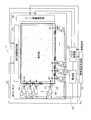
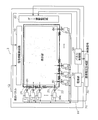
- FIG. 1 is a block diagram showing an example of a functional configuration of an organic EL display device 1 according to an embodiment of the present invention.
- a display panel 10 having a feedback circuit unit 80 is provided instead of the display panel 19 of the organic EL display device 9 of FIG. 19 described in the section of the prior art, and a reference voltage generation unit 70, a reference voltage A line 71 is added.
- a reference voltage generation unit 70 a reference voltage A line 71 is added.
- FIG. 1 the internal structure of the display part 20 is shown in detail.
- a plurality of pixel units 30 including the organic EL elements 33 are arranged in a planar shape.
- a plurality of first power supply lines 31 are branched from the connection portions 22 of the bus wiring 21 and extended into the display portion 20.
- a plurality of second power supply lines 32 are provided in the display unit 20.
- the first electrode (anode) of the organic EL element 33 is electrically connected to the first power line 31, and the second electrode (cathode) of the organic EL element 33 is electrically connected to the second power line 32.
- the signal line driving circuit 40 supplies a luminance signal to the pixel unit 30 via the signal line 41.
- the gate line driving circuit 42 supplies a scanning signal to the pixel unit 30 through the gate line 43.
- the pixel unit 30 acquires a luminance signal from the signal line 41 in response to the scanning signal applied from the gate line 43, and causes the organic EL element 33 to emit light with the luminance indicated by the acquired luminance signal.
- the organic EL element 33 emits light with current supplied from the first power supply line 31 and the second power supply line 32.
- the power supply unit 60 supplies a power supply voltage for driving each feedback circuit unit 80 to each feedback circuit unit 80 via the wiring 61.
- the wiring 61 is composed of, for example, two wirings for supplying a high potential and a low potential of the power supply voltage.
- the reference voltage generation unit 70 generates a reference voltage for defining a target voltage applied to the voltage of the bus wiring 21, and supplies the generated reference voltage to each feedback circuit unit 80 via the reference voltage line 71. To do.
- the feedback circuit unit 80 is a voltage regulator based on feedback control, and generates an output voltage from a power supply voltage supplied via the wiring 61.
- the feedback circuit unit 80 feedback-controls the generated output voltage so that the voltage at the connection unit 22 of the bus wiring 21 is equal to the target voltage defined by the reference voltage applied from the reference voltage generation unit 70. To do.
- the generated output voltage is applied to the connection portion 22 which is a part of the bus wiring 21 via the wiring resistance.
- the arrangement of the feedback circuit unit 80, the connection unit 22, and the first power supply line 31 is not limited to the example shown in FIG.
- the feedback circuit unit 80 is provided in at least one of the left and right peripheral parts of the display unit 20, and is provided only in the left peripheral part of the display unit 20 as shown in FIG. 20 may be provided only at the right peripheral portion, or may be provided at the left and right peripheral portions. Further, the feedback circuit unit 80 is provided in at least one of the upper and lower peripheral portions of the display unit 20, and is provided only in the lower peripheral portion of the display unit 20 as shown in FIG. It may be provided only in the peripheral part on the upper side of the part 20, and may be provided in the peripheral part on both the upper and lower sides.
- the feedback circuit unit 80 is connected to the bus wiring 21 on the short side and the long side of the display unit 20, and the first power supply line 31 is arranged in the horizontal and vertical directions of the display unit 20.
- the feedback circuit unit 80 may be connected to the bus wiring 21 only on the short side of the display unit 20, and the first power supply line 31 may be arranged only in the lateral direction of the display unit 20.
- the unit 80 may be connected to the bus wiring 21 only on the long side of the display unit 20, and the first power supply line 31 may be arranged only in the vertical direction of the display unit 20.
- FIG. 2 is a block diagram showing an example of a main part of the organic EL display device 1 including the feedback circuit unit 80 and the connection part 22 of the bus wiring 21.
- the feedback circuit unit 80 includes a first power supply terminal 83a, a second power supply terminal 83b, a first input terminal 84, a second input terminal 86, and an output terminal 85.
- the high potential and the low potential of the power supply voltage are applied to the first power supply terminal 83a and the second power supply terminal 83b through the wirings 61a and 61b constituting the wiring 61, respectively.
- a reference voltage is applied to the first input terminal 84 via a reference voltage line 71.
- the output terminal 85 is connected to the connection unit 22 via the feeder 81 and the second input terminal 86 is connected to the connection unit 22 via the monitor line 82.
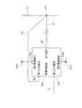
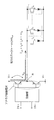
- FIG. 3 is a circuit diagram of a feedback circuit unit 80 a as a specific example of the feedback circuit unit 80.
- the feedback circuit unit 80a includes an error amplifier 87.
- the error amplifier 87 operates with a power supply voltage applied to the first power supply terminal 83a and the second power supply terminal 83b.
- the voltage V CONN of the connection unit 22 is applied as the monitor voltage V MON to the negative input of the error amplifier 87.
- a reference voltage V REF is applied to the plus input of the error amplifier 87.
- the error amplifier 87 adjusts the output voltage at the output terminal 85 by comparing the monitor voltage VMON with the reference voltage VREF .
- the monitor voltage VMON is adjusted to be a voltage obtained by adding the voltage drop amount obtained by the product of the resistance of the power supply line 81 and the current flowing through the output terminal 85 to the monitor voltage VMON .
- the output voltage from the feedback circuit unit 80a increases or decreases so as to cancel the voltage drop generated in the resistance of the power supply line 81, so that the voltage V CONN of the connection unit 22 is maintained equal to the reference voltage V REF. Is done. As a result, the voltage at each connection portion 22 of the bus wiring 21 is equalized to the target voltage regardless of the display pattern.
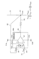
- FIG. 4 is a circuit diagram of a feedback circuit unit 80b as another specific example of the feedback circuit unit 80.
- the feedback circuit unit 80b includes a third power supply terminal 83c and gain resistors R1 and R2.
- a reference voltage VREF as a first reference voltage is applied to the first input terminal 84
- a bias voltage VBIAS as a second reference voltage is applied to the third power supply terminal 83c.
- Gain resistor R1, R2 is a voltage applied between the first input terminal 84 and the second input terminal 86, that is, dividing the difference voltage between the monitor voltage V MON and the reference voltage V REF. The divided voltage is applied to the negative input of the error amplifier 87.
- the bias voltage V BIAS may be generated by the reference voltage generation unit 70 and supplied via a wiring (not shown). Also, 0 V that is the ground voltage may be used as the bias voltage V BIAS . Bias voltage V BIAS is applied to the positive input of error amplifier 87.
- the reference voltage V REF as the first reference voltage is a voltage having a lower potential than the output voltage from the feedback circuit unit 80b, and the absolute value of the output voltage output from the feedback circuit unit 80b is determined from the absolute value. This is a reference voltage for conversion to a small potential voltage.
- the bias voltage V BIAS as the second reference voltage is a voltage having a lower potential than the output voltage from the feedback circuit unit 80b, and is a reference voltage for adjusting the output voltage.
- the voltage V CONN of the connection unit 22 is defined by the reference voltage V REF and the bias voltage V BIAS.
- the target voltage is maintained at ⁇ (R 2 / R 1 ) V REF + (1 + R 2 / R 1 ) V BIAS .
- a voltage obtained by multiplying the reference voltage V REF by a gain larger than 1 is a target voltage for the voltage V CONN of the connection unit 22.
- a desired target voltage can be defined using the low-voltage reference voltage V REF , so that the reference voltage generation unit 70 can have a low-voltage circuit configuration, and the circuit in the reference voltage generation unit 70 It is possible to reduce the area and power consumption.
- FIG. 5 is a circuit diagram of a feedback circuit unit 80c as another specific example of the feedback circuit unit 80.
- a third power supply terminal 83c to which the bias voltage V BIAS is applied is added to the feedback circuit unit 80a, and gain resistors R1 and R2 are added.
- the bias voltage V BIAS may be supplied from the reference voltage generation unit 70, or 0 V that is a ground voltage may be used.
- the voltage V CONN of the connection unit 22 is defined by the reference voltage V REF and the bias voltage V BIAS.
- the target voltage is maintained to be (1 + R 2 / R 1 ) V REF + (R 2 / R 1 ) V BIAS .
- a voltage obtained by multiplying the reference voltage V REF by a gain larger than 1 is used as a target voltage for the voltage V CONN of the connection unit 22 regardless of the resistance values of the gain resistors R1 and R2.
- a desired target voltage can be defined using the low-voltage reference voltage V REF , so that the reference voltage generation unit 70 can have a low-voltage circuit configuration, and the circuit in the reference voltage generation unit 70 It is possible to reduce the area and power consumption.
- FIG. 6 is a diagram illustrating an example of a display result obtained when the image used in the description of FIG. 19 is displayed on the organic EL display device 1.
- the voltage at each connection portion 22 of the bus wiring 21 is equalized to the target voltage V corresponding to the reference voltage.
- Display quality degradation i.e., the inconvenience of non-uniform luminance within an area to be displayed with uniform luminance is alleviated.
- the voltage at the connection part 22 of the bus line 21 is maintained at the target voltage defined by the reference voltage V REF by the feedback circuit unit 80. Therefore, the voltage at each connection portion 22 of the bus wiring 21 becomes uniform regardless of the display pattern. As a result, even when an image including a high luminance area is displayed, the luminance in the vicinity of the high luminance area does not decrease, and the display quality is improved. Further, since it is not necessary to reduce the resistance of the bus wiring 21, it is not necessary to provide the bus wiring in a large area, which is suitable for narrow frame.
- An independent reference voltage may be applied to each feedback circuit unit 80, and the target voltage V at each connection unit 22 of the bus wiring 21 may be a different voltage depending on the display pattern.
- FIG. 7 is a block diagram showing an example of a functional configuration of the organic EL display device 2 according to such a modification.
- the display panel 11 is provided with a reference voltage line 73 composed of a plurality of wirings provided corresponding to each of the feedback circuit units 80.
- the reference voltage generation unit 72 generates an independent reference voltage for each feedback circuit unit 80 and applies the generated reference voltage to the feedback circuit unit 80 via a corresponding wiring in the reference voltage line 73.
- a higher reference voltage than that for the other feedback circuit units 80 may be applied to the feedback circuit unit 80 located near the high luminance region.
- the voltage drop generated in the first power supply line 31 extending from the connection portion 22 to the inside of the display portion 20 is compensated, so that it is expected that the display quality is further improved.
- connection unit 22 Next, a more practical configuration of the connection unit 22 will be described.
- the output terminal 85 and the second input terminal 86 of the feedback circuit unit 80 have been described only as being connected to the connection unit 22 that is a part of the bus wiring 21.
- the terminal 85 is connected to a region having a certain size in the connection portion 22 of the bus wiring 21 through the feeder line 81 and the second input terminal 86 through the monitor line 82.
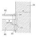
- FIGS. 8A and 8B are plan views showing an example of the wiring shape of the bus wiring 21, the power supply line 81, and the monitor line 82 in the vicinity of the connecting portion 22, and the power supply line is connected to the bus wiring 21 from the left side of the drawing. A state in which 81 and a monitor line 82 are connected is shown.
- a region where the bus wiring 21 is connected to each of the feeder line 81 and the monitor line 82 is indicated by a dotted box.
- the center point of the connection region between the bus line 21 and the power supply line 81 is defined as a power supply point 23
- the center point of the connection region between the bus line 21 and the monitor line 82 is defined as a monitor point 24.
- FIG. 9 is an equivalent circuit diagram corresponding to such a practical configuration.
- the feeding point 23 and the monitor point 24 are provided at different positions on the bus wiring 21, and are connected by the resistance of the bus wiring 21.
- the resistance value of the power supply line 81 is R 1
- the voltage drop amount generated in the power supply line 81 is ⁇ V R1
- the resistance value of the bus wiring 21 between the power supply point 23 and the monitor point 24 is R 2
- the connection unit 22 and the monitor point 24 when the voltage drop amount is [Delta] V R2 that occurs between the voltage V CONN feed point 23 is maintained at a [Delta] V R2 voltage higher than the voltage V MON monitor point 24.
- the voltage V MON at the monitor point 24 is maintained at the target voltage
- the drive voltage supplied to the pixel unit 30 is the voltage V CONN at the power supply point 23, so ⁇ V R2 is the target of the drive voltage. It becomes an error for the voltage.
- the distance d between the feeding point 23 and the monitoring point 24 is set to the bus wiring 21. It is defined that the width is less than or equal to w. That is, FIG. 8A shows an example of a shape in which the feeding point 23 and the monitoring point 24 are provided closest to each other, and FIG. 8B shows a shape in which the feeding point 23 and the monitoring point 24 are provided most apart. An example is shown.
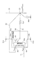
- FIG. 10 is a circuit diagram of a feedback circuit unit 90a as still another specific example of the feedback circuit unit 80.
- the connecting part 22 is simplified again.
- the feedback circuit unit 90 a is an example of a fundamental feedback circuit unit that performs a switching operation, and includes a switching control circuit 91 a and a transistor 92.
- V CONN the voltage V CONN of the connection unit 22
- V REF the gate signal V G of the level V on that turns on the transistor 92
- the voltage V CONN is If it is determined that the voltage is higher than the target voltage, a gate signal V G of level V off that shuts off the transistor 92 is output.
- Transistor 92 is connected to one source-drain terminal to the first power supply terminal 83a is connected to the other of the source drain terminal to the output terminal 85, in response to the gate signal V G applied from the switching control circuit 91a, the first The power supply voltage applied to the power supply terminal 83a is supplied to the output terminal 85 or cut off.
- the voltage V CONN of the connection part 22 is smoothed by the capacitor 88a which is the capacity of the first power supply line 31 (FIG. 1) extending from the bus line 21 and the connection part 22 to the inside of the display part 20.
- the capacitor 88a may be a panel parasitic capacitance.
- a capacitor element that includes a first electrode and a second electrode, the first electrode is connected to the bus wiring 21, and the second electrode is connected to a fixed potential may be provided.
- the feedback circuit unit 90a includes a switching control circuit 91a and a transistor 92, and the switching control circuit 91a controls on / off of the transistor 92.
- the transistor 92 having one terminal connected to the power supply terminal 83a and the other terminal connected to the output terminal 85 is used, so that the voltage at the connection section 22 of the bus wiring 21 is the target.
- the transistor 92 is cut off.
- the transistor 92 is turned on to have a low resistance (ideally zero ohms). Thereby, the power loss which occurs in the comparative example using the operational amplifier can be reduced, and the target voltage can be efficiently supplied from the power supply voltage to the output terminal.
- FIG. 11 is a timing chart showing an example of the operation of the feedback circuit unit 90a.
- the power supply voltage applied to the first power supply terminal 83a is expressed as VDD 1
- the target voltage defined by the reference voltage V REF is expressed as VDD.
- FIG. 11 shows two examples of waveforms corresponding to different pixel currents. Specifically, the left waveform in FIG. 11 shows a case where a large pixel current flows because a bright image is displayed, and the small waveform current flows because the right waveform in FIG. 11 displays a dark image. Shows the case.
- the gate signal V G becomes the V on level and the transistor 92 is turned on
- the power supply voltage VDD 1 applied to the first power supply terminal 83a is supplied from the output terminal 85 to the connection portion 22, and the output current i having a magnitude of i on. OUT flows.
- the voltage V CONN of the connection unit 22 increases toward VDD 1 with a time constant determined by the capacitance of the first power supply line 31 in the bus line 21 and the display unit 20 and i on .
- the gate signal V G becomes V off level after the inherent delay time by the switching control circuit 91a, and the transistor 92 is turned off.
- the inherent delay time is the time when the voltage V CONN of the connection unit 22 actually exceeds the target voltage VDD and after that time, and the switching control circuit compares the voltage V CONN with the target voltage VDD, and the transistor 92 Is the time difference from when the operation to turn off is started.
- the voltage V CONN of the connection unit 22 is the capacitance of the first power supply line 31 in the bus line 21 and the display unit 20 and the resistance component of the pixel circuit group constituting the display unit (the resistance component is the voltage V CONN changes per unit voltage).
- the rate of change of the panel current value at the time that is, when displaying a bright image, the time constant is relatively small compared to when displaying a dark image and dark
- the voltage drops to 0 V, which is the ground voltage (with a relatively large time constant compared to when a bright picture is displayed).
- the on-current i on the results of flow intermittently, as an average value of the output current i OUT, small average when a large average current i a flows, displaying dark image when displaying the bright image current i b flows.
- the gate signal V G becomes V on level after the inherent delay time of the switching control circuit 91a, and the transistor 92 is turned on.
- the voltage V CONN of the connection unit 22 is maintained in a predetermined voltage range including the target voltage VDD.
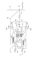
- FIG. 12 is a circuit diagram of a feedback circuit unit 90b as still another specific example of the feedback circuit unit 80.
- the feedback circuit unit 90b is an example of a more practical feedback circuit unit that performs a PWM (pulse width modulation) switching operation, and includes a switching control circuit 91b, transistors 92 and 93, and a coil 94.
- the switching control circuit 91b includes an error amplifier 95, a PWM comparator 96, a PWM controller 97, and a triangular wave generator 98.
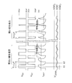
- FIG. 13 is a timing chart illustrating an example of the operation of the feedback circuit unit 90b.
- the power supply voltage applied to the first power supply terminal 83a is VDD 1
- target voltage power supply voltage applied to the second power supply terminal 83b is defined by VDD 2
- reference voltage V REF is denoted as VDD .
- FIG. 13 shows two examples of waveforms corresponding to different pixel currents depending on the brightness of the displayed image, as in FIG.
- the transistor 92 is ON, the transistor 93 is OFF, and the coil 94 is connected to the first power supply terminal 83a. To do.
- the voltage V CONN of the connection unit 22 tends to approach the power supply voltage VDD 1 applied to the first power supply terminal 83a.
- the PWM controller 97 sequentially changes the levels of the gate signals V G1 and V G2. By turning over the transistor 92 by giving a time difference, the transistor 93 is turned on. As a result, the connection of the coil 94 is switched from the first power supply terminal 83a to the second power supply terminal 83b.
- the output current i OUT flowing from the first power supply terminal 83a to the output terminal 85 via the transistor 92 and the coil 94 is not detected by the self-induction of the coil 94 even after the connection of the coil 94 is switched. It continues to flow from the power supply terminal 83b to the output terminal 85 via the transistor 93 and the coil 94.
- the self-induction energy stored in the coil 94 decreases with time, the output current i OUT decreases, the voltage of the output terminal 85 decreases, and the voltage V CONN of the connection portion 22 is equal to the voltage of the second power supply terminal 83b. When it approaches the VDD 2.
- the PWM controller 97 sequentially changes the levels of the gate signals V G2 and V G1. By turning over the transistor 93 by giving a time difference, the transistor 92 is turned on. As a result, the connection of the coil 94 is switched from the second power supply terminal 83b to the first power supply terminal 83a.
- the voltage V CONN of the connection unit 22 is maintained in a predetermined voltage range including the target voltage VDD.
- the configuration in which the bus wiring 21 is used as a positive power source for each pixel unit 30 has been described.
- the driving voltage of the bus line 21 controlled to the target voltage by the feedback circuit unit 80 is used as the power supply voltage on the higher side for each pixel unit 30.
- a pixel current is supplied to each pixel unit 30.
- FIG. 14 is a block diagram showing an example of a functional configuration of the organic EL display device 3 using the bus wiring 21 as a negative power source.
- a display panel 12 is used instead of the display panel 10 of the organic EL display device 1 of FIG.
- the display panel 12 includes a feedback circuit unit 90 c capable of supplying a negative power supply, and a plurality of second power supply lines 32 are branched from the connection portions 22 of the bus wiring 21 and extended into the display unit 25.
- a plurality of first power lines 31 are provided in the display unit 25.
- the first electrode (anode) of the organic EL element 33 is electrically connected to the first power supply line 31 via the drive transistor, and the second electrode (cathode) of the organic EL element 33 is electrically connected to the second power supply line 32. It is connected to the.
- the driving voltage of the bus wiring 21 controlled to the target voltage by the feedback circuit unit 90 c is used as the lower power supply voltage for each pixel unit 30.
- a pixel current is drawn from the pixel unit 30 to the bus line 21.
- FIG. 16 is a circuit diagram showing an example of the feedback circuit unit 90c.
- the function of the switching control circuit 91c and the connection of the transistor 92 are changed as compared with the feedback circuit unit 90a of FIG.
- V CONN the voltage V CONN of the connection unit 22
- V REF the reference voltage
- the gate signal V G of the level V on that turns on the transistor 92 is output, and the voltage V CONN is and it outputs a gate signal V G of level V off to cut off the transistor 92 when it is determined to be smaller than the target voltage.
- Transistor 92 is connected to one source-drain terminal to the second power supply terminal 83 b is connected to the other of the source drain terminal to the output terminal 85, in response to the gate signal V G applied from the switching control circuit 91c, a second The power supply voltage applied to the power supply terminal 83b is supplied to the output terminal 85 or cut off.
- the voltage V CONN of the connection part 22 is smoothed by the capacitor 88b which is the capacity of the second power supply line 32 (FIG. 14) extending from the bus line 21 and the connection part 22 to the inside of the display part 25.
- FIG. 17 is a timing chart showing an example of the operation of the feedback circuit unit 90c.
- the target voltage power supply voltage applied to the second power supply terminal 83b is defined by VDD 2
- reference voltage V REF is denoted as VDD.
- the output current of the feedback circuit unit 90c is expressed as -i out in consideration of the suction direction.
- FIG. 17 shows two examples of waveforms corresponding to different pixel currents depending on the brightness of the displayed image, as in FIG.
- the feedback circuit unit 90c operates symmetrically with the feedback circuit unit 90a. By such an operation, the voltage V CONN at the connection portion 22 of the bus wiring 21 is maintained in a predetermined voltage range including the target voltage VDD.
- the organic EL display devices 1 to 3 that equalize the voltage of the bus wiring by the feedback circuit unit, the organic EL display device in which the feedback circuit unit is configured using an error amplifier, and a switching control circuit (for example, DC voltage conversion)
- a specific example of an organic EL display device in which a feedback circuit unit is configured using a display device or a DC-DC converter has been described.
- Such organic EL display devices 1 to 3 can be used to display high-quality images in various devices such as a television set, a personal computer, and a portable information terminal.
- FIG. 18 is an external view showing the external appearance of the television set 100 using the organic EL display device 1, 2 or 3.
- the organic EL display devices 1, 2, or 3 for example, an image partially including a high luminance region is displayed, and uneven luminance in regions other than the high luminance region is suppressed. Can be displayed in high quality.
- the organic EL display device of the present invention has been described based on the embodiments.
- the present invention is not limited to these embodiments. Unless it deviates from the meaning of this invention, the form obtained by combining each embodiment with the various deformation
- the present invention can be applied to a video display device such as an organic EL display device.
Landscapes
- Engineering & Computer Science (AREA)
- Physics & Mathematics (AREA)
- Computer Hardware Design (AREA)
- General Physics & Mathematics (AREA)
- Theoretical Computer Science (AREA)
- Electroluminescent Light Sources (AREA)
- Control Of Indicators Other Than Cathode Ray Tubes (AREA)
- Control Of El Displays (AREA)
Abstract
Description
以下、本発明の実施の形態に係る有機EL表示装置について、図面を参照しながら詳細に説明する。
10、11、12、19 表示パネル
20、25 表示部
21 バス配線
22 接続部
23 給電点
24 モニター点
30 画素部
31 第1電源線
32 第2電源線
33 有機EL素子
40 信号線駆動回路
41 信号線
42 ゲート線駆動回路
43 ゲート線
50 パネル制御部
60 電源部
61、61a、61b 配線
70、72 基準電圧生成部
71、73 基準電圧線
80、80a、80b、80c、90a、90b、90c 帰還回路部
81 給電線
82 モニター線
83a 第1電源端子
83b 第2電源端子
83c 第3電源端子
84 第1入力端子
85 出力端子
86 第2入力端子
87 誤差増幅器
88a、88b コンデンサ
91a、91b、91c スイッチング制御回路
92、93 トランジスタ
94 コイル
95 誤差増幅器
96 PWM比較器
97 PWM制御器
98 三角波生成器
100 テレビジョンセット
Claims (20)
- 基板上に有機EL素子を含む画素部を複数配置した表示部と、
前記表示部の外周に配置され、前記表示部に含まれる各画素部を駆動するための駆動電圧を各画素部に供給する電源バス配線と、
出力電圧を生成して前記電源バス配線に供給する帰還回路部と、
前記帰還回路部を駆動するための高電源電圧と前記高電源電圧よりも低い低電源電圧とからなる電源電圧を前記帰還回路部に供給する電源部と、
前記電源バス配線の電圧に適用される目標電圧を規定する基準電圧を前記帰還回路部に供給する基準電圧生成部と、を具備し、
前記帰還回路部は、前記電源部から供給された電源電圧に基づいて前記出力電圧を生成し、
前記帰還回路部は、
前記電源電圧のうち前記高電源電圧が印加される第1電源端子と、
前記電源電圧のうち前記低電源電圧が印加される第2電源端子と、
前記基準電圧が印加される第1入力端子と、
前記電源バス配線の一部である接続部と接続された出力端子と、
前記電源バス配線の前記接続部での電圧が印加される第2入力端子と、
前記第1電源端子、前記第2電源端子、前記第1入力端子、及び前記第2入力端子と接続されたスイッチング制御回路と、
一方の端子を前記第1電源端子及び前記第2電源端子のうちのいずれか一方の電源端子に接続され、他方の端子を前記出力端子に接続されたトランジスタと、を含み、
前記トランジスタのオンとオフとに応じて、前記一方の電源端子に印加される前記電源電圧を前記出力端子に供給するかまたは遮断することにより、前記電源バス配線の前記接続部での電圧が前記基準電圧で規定される前記目標電圧と等しくなるように、前記電源バス配線の前記接続部での電圧に差分を加算した電圧を前記出力電圧として前記出力端子に出力し、
加算される前記差分は、
前記帰還回路部の出力端子と前記電源バス配線の前記接続部との間の抵抗と、前記帰還回路部の出力端子と前記電源バス配線の前記接続部との間に流れる電流と、の積によって求められる電圧降下量に対応する、
有機EL表示装置。 - さらに、第1電極と第2電極とを有し、前記第1電極が前記バス配線と接続され、前記第2電極が固定電位に接続される容量素子を備える、
請求項1に記載の有機EL表示装置。 - 前記スイッチング制御回路は、
比較器により前記接続部での電圧と前記基準電圧とを用いた比較動作を行い、前記接続部での電圧が、前記基準電圧で規定される前記目標電圧よりも小さいと判定されると前記トランジスタをオンさせるレベルVonのゲート信号を出力し、前記接続部での電圧が前記目標電圧より大きいと判定されるとトランジスタを遮断させるレベルVoffのゲート信号を出力する、
請求項1又は2に記載の有機EL表示装置 - 前記帰還回路部は、
前記電源バス配線の前記接続部での電圧が、前記目標電圧より大きいと判定すると、前記出力電圧の供給を停止して前記駆動電圧を低減する、
請求項1から請求項3のいずれか1項に記載の有機EL表示装置。 - 前記帰還回路部は、
前記電源バス配線の前記接続部での電圧が、前記目標電圧より小さいと判定すると、前記出力電圧の供給を再開して前記駆動電圧を増加する、
請求項4に記載の有機EL表示装置。 - 前記帰還回路部は、
前記電源バス配線の前記接続部での電圧が、前記目標電圧より小さいと判定すると、前記出力電圧の供給を停止して前記駆動電圧を増加する、
請求項1から請求項3のいずれか1項に記載の有機EL表示装置。 - 前記帰還回路部は、
前記電源バス配線の前記接続部での電圧が、前記目標電圧より大きいと判定すると、前記出力電圧の供給を再開して前記駆動電圧を低減する、
請求項6に記載の有機EL表示装置。 - さらに1つ以上の帰還回路部が設けられ、
前記複数の帰還回路部は、前記電源バス配線と複数の接続部にて接続されている、
請求項1から請求項7のいずれか1項に記載の有機EL表示装置。 - 前記複数の接続部の各々は、前記電源バス配線において一定の間隔で設けられている、
請求項8に記載の有機EL表示装置。 - 前記複数の帰還回路部の各々は、
前記第1入力端子に入力された前記基準電圧に1よりも大きいゲインを乗じて得られる電圧を前記目標電圧として設定する、
請求項8又は9に記載の有機EL表示装置。 - 前記複数の帰還回路部の各々は、
前記第1入力端子に入力された前記基準電圧を前記目標電圧として設定し、前記電源バス配線の前記接続部での電圧が前記基準電圧と等しくなるように前記電源バス配線の前記接続部での電圧を増減させる、
請求項10に記載の有機EL表示装置。 - 前記複数の帰還回路部の各々は、前記表示部の左右の少なくとも一方の周辺部に設けられる、
請求項8から請求項11のいずれか1項に記載の有機EL表示装置。 - 前記複数の帰還回路部の各々は、前記表示部の上下の少なくとも一方の周辺部に設けられる、
請求項1から請求項12のいずれか1項に記載の有機EL表示装置。 - 各画素部に含まれる前記有機EL素子の第1電極に電気的に接続される複数の第1電源線と、
各画素部に含まれる前記有機EL素子の第2電極に電気的に接続される複数の第2電源線と、を有し、
前記複数の第1電源線及び前記複数の第2電源線のうちの一方は、前記電源バス配線に接続される、
請求項1から請求項13のいずれか1項に記載の有機EL表示装置。 - 前記複数の帰還回路部の各々は、前記電源バス配線の短辺側で前記電源バス配線に接続され、
前記複数の第1電源線及び前記複数の第2電源線の前記一方は、前記複数の帰還回路部の各々の出力端子と前記電源バス配線との各接続部から分岐して前記表示部の横方向に配置される、
請求項14に記載の有機EL表示装置。 - 前記複数の帰還回路部の各々は、前記電源バス配線の長辺側で前記電源バス配線に接続され、
前記複数の第1電源線及び前記複数の第2電源線の前記一方は、前記複数の帰還回路部の各々の出力端子と前記電源バス配線との各接続部から分岐して前記表示部の縦方向に配置される、
請求項14に記載の有機EL表示装置。 - 前記複数の帰還回路部の各々は、前記電源バス配線の短辺側及び長辺側で前記電源バス配線に接続され、
前記複数の第1電源線及び前記複数の第2電源線の前記一方は、前記複数の帰還回路部の各々の出力端子と前記電源バス配線との各接続部から分岐して前記表示部の横方向及び縦方向に配置される、
請求項14に記載の有機EL表示装置。 - 前記電源バス配線は、前記表示部の外周に環状に設けられる、
請求項1から請求項17のいずれか1項に記載の有機EL表示装置。 - 前記接続部は、
前記帰還回路部の前記出力端子に給電線を介して接続される給電点と、
前記帰還回路部の前記出力端子にモニター線を介して接続されるモニター点と、
を有し、
前記給電点と前記モニター点との距離は前記電源バス配線の配線幅以下である、
請求項1から請求項18のいずれか1項に記載の有機EL表示装置。 - 基板上に有機EL素子を含む画素部を複数配置した表示部と、
前記表示部の外周に配置され、前記表示部に含まれる各画素部を駆動するための駆動電圧を各画素部に供給する電源バス配線と、
出力電圧を生成して前記電源バス配線に供給する帰還回路部と、
前記帰還回路部を駆動するための電源電圧を前記帰還回路部に供給する電源部と、
前記帰還回路部から出力される駆動電圧より低い電位の電圧であって前記帰還回路部から出力される駆動電圧の絶対値を当該絶対値より小さい電位の電圧に変換するための第1基準電圧を前記帰還回路部に供給し、前記帰還回路部から出力される駆動電圧より低い電位の電圧であって前記変換された電圧を調整する基準となる第2基準電圧を前記帰還回路部に供給する基準電圧生成部と、を具備し、
前記帰還回路部は、前記電源部から供給された電源電圧に基づいて前記出力電圧を生成し、
前記帰還回路部は、
前記電源電圧が印加される電源端子と、
前記電源バス配線の一部である接続部と接続された出力端子と、
前記第1基準電圧が印加される第1入力端子と、
前記電源バス配線の前記接続部での電圧が印加される第2入力端子と、
前記第2基準電圧が印加される第3電源端子と、
前記第1入力端子と前記第2入力端子との間に直列に設けられ、前記第1入力端子と前記第2入力端子との間に印加された電圧を分圧する第1抵抗及び第2抵抗と、を含み、
前記第1抵抗および前記第2抵抗にて分圧された電圧が前記第2基準電圧と等しくなるように、前記電源バス配線の前記接続部での電圧に差分を加算した電圧を前記出力電圧として前記出力端子に出力し、
加算される前記差分は、
前記帰還回路部の出力端子と前記電源バス配線の前記接続部との間の抵抗と、前記帰還回路部の出力端子と前記電源バス配線の前記接続部との間に流れる電流と、の積によって求められる電圧降下量に対応する、
有機EL表示装置。
Priority Applications (3)
| Application Number | Priority Date | Filing Date | Title |
|---|---|---|---|
| CN201180016636.XA CN102834858B (zh) | 2010-07-29 | 2011-07-28 | 有机el显示装置 |
| JP2012526330A JP5485396B2 (ja) | 2010-07-29 | 2011-07-28 | 有機el表示装置 |
| US13/684,807 US9384690B2 (en) | 2010-07-29 | 2012-11-26 | Organic EL display apparatus |
Applications Claiming Priority (2)
| Application Number | Priority Date | Filing Date | Title |
|---|---|---|---|
| JP2010171143 | 2010-07-29 | ||
| JP2010-171143 | 2010-07-29 |
Related Child Applications (1)
| Application Number | Title | Priority Date | Filing Date |
|---|---|---|---|
| US13/684,807 Continuation US9384690B2 (en) | 2010-07-29 | 2012-11-26 | Organic EL display apparatus |
Publications (1)
| Publication Number | Publication Date |
|---|---|
| WO2012014477A1 true WO2012014477A1 (ja) | 2012-02-02 |
Family
ID=45529708
Family Applications (1)
| Application Number | Title | Priority Date | Filing Date |
|---|---|---|---|
| PCT/JP2011/004274 Ceased WO2012014477A1 (ja) | 2010-07-29 | 2011-07-28 | 有機el表示装置 |
Country Status (4)
| Country | Link |
|---|---|
| US (1) | US9384690B2 (ja) |
| JP (1) | JP5485396B2 (ja) |
| CN (1) | CN102834858B (ja) |
| WO (1) | WO2012014477A1 (ja) |
Cited By (5)
| Publication number | Priority date | Publication date | Assignee | Title |
|---|---|---|---|---|
| CN104050915A (zh) * | 2014-05-30 | 2014-09-17 | 京东方科技集团股份有限公司 | Amoled 显示面板和amoled 显示装置 |
| JP2016520872A (ja) * | 2013-05-17 | 2016-07-14 | タレス | 大型ピクセルマトリクスを備える電気光学装置 |
| JP2017142440A (ja) * | 2016-02-12 | 2017-08-17 | セイコーエプソン株式会社 | 電気光学装置および電子機器 |
| JP2021051143A (ja) * | 2019-09-24 | 2021-04-01 | ラピスセミコンダクタ株式会社 | レベル電圧生成回路、データドライバ及び表示装置 |
| US11430392B2 (en) | 2019-12-26 | 2022-08-30 | Seiko Epson Corporation | Display device and electronic apparatus |
Families Citing this family (10)
| Publication number | Priority date | Publication date | Assignee | Title |
|---|---|---|---|---|
| CN103927968B (zh) * | 2013-06-18 | 2016-12-28 | 上海天马微电子有限公司 | 一种oled显示装置 |
| KR102241848B1 (ko) * | 2014-08-12 | 2021-04-20 | 삼성디스플레이 주식회사 | 전원 공급 장치 및 이를 포함하는 유기발광 표시장치 |
| CN107966838B (zh) * | 2017-12-18 | 2020-09-18 | 深圳市华星光电技术有限公司 | 一种液晶面板及显示装置 |
| CN108922487B (zh) * | 2018-08-24 | 2020-06-26 | 惠科股份有限公司 | 电压调节电路及显示装置 |
| CN111028754A (zh) | 2019-12-06 | 2020-04-17 | 深圳市华星光电半导体显示技术有限公司 | 显示面板 |
| CN110956920A (zh) * | 2019-12-24 | 2020-04-03 | 武汉天马微电子有限公司 | 显示装置及其驱动方法 |
| KR102721850B1 (ko) * | 2019-12-27 | 2024-10-24 | 엘지디스플레이 주식회사 | 발광표시장치 및 이의 구동방법 |
| CN111524485B (zh) * | 2020-05-29 | 2021-12-31 | 京东方科技集团股份有限公司 | Oled模组外部驱动电路及驱动方法、显示装置 |
| KR102888465B1 (ko) * | 2020-12-08 | 2025-11-20 | 엘지디스플레이 주식회사 | 전계 발광 표시장치 |
| JP2022163267A (ja) * | 2021-04-14 | 2022-10-26 | シャープディスプレイテクノロジー株式会社 | 発光装置、表示装置、およびled表示装置 |
Citations (4)
| Publication number | Priority date | Publication date | Assignee | Title |
|---|---|---|---|---|
| JPH08171081A (ja) * | 1994-12-19 | 1996-07-02 | Sharp Corp | マトリクス型表示装置 |
| JPH09281928A (ja) * | 1996-04-16 | 1997-10-31 | Pioneer Electron Corp | 表示装置 |
| JP2002032037A (ja) * | 2000-05-12 | 2002-01-31 | Semiconductor Energy Lab Co Ltd | 表示装置 |
| JP2005236848A (ja) * | 2004-02-23 | 2005-09-02 | Toshiba Microelectronics Corp | 半導体集積回路及びその内部電源立ち下げ方法 |
Family Cites Families (5)
| Publication number | Priority date | Publication date | Assignee | Title |
|---|---|---|---|---|
| TW554638B (en) * | 2000-05-12 | 2003-09-21 | Semiconductor Energy Lab | Light emitting device |
| US8610645B2 (en) | 2000-05-12 | 2013-12-17 | Semiconductor Energy Laboratory Co., Ltd. | Display device |
| JP3858590B2 (ja) | 2000-11-30 | 2006-12-13 | 株式会社日立製作所 | 液晶表示装置及び液晶表示装置の駆動方法 |
| KR100583139B1 (ko) | 2004-10-08 | 2006-05-23 | 삼성에스디아이 주식회사 | 발광 표시장치 |
| KR100720143B1 (ko) | 2005-12-13 | 2007-05-18 | 삼성전자주식회사 | 디스플레이장치 |
-
2011
- 2011-07-28 JP JP2012526330A patent/JP5485396B2/ja active Active
- 2011-07-28 CN CN201180016636.XA patent/CN102834858B/zh active Active
- 2011-07-28 WO PCT/JP2011/004274 patent/WO2012014477A1/ja not_active Ceased
-
2012
- 2012-11-26 US US13/684,807 patent/US9384690B2/en active Active
Patent Citations (4)
| Publication number | Priority date | Publication date | Assignee | Title |
|---|---|---|---|---|
| JPH08171081A (ja) * | 1994-12-19 | 1996-07-02 | Sharp Corp | マトリクス型表示装置 |
| JPH09281928A (ja) * | 1996-04-16 | 1997-10-31 | Pioneer Electron Corp | 表示装置 |
| JP2002032037A (ja) * | 2000-05-12 | 2002-01-31 | Semiconductor Energy Lab Co Ltd | 表示装置 |
| JP2005236848A (ja) * | 2004-02-23 | 2005-09-02 | Toshiba Microelectronics Corp | 半導体集積回路及びその内部電源立ち下げ方法 |
Cited By (10)
| Publication number | Priority date | Publication date | Assignee | Title |
|---|---|---|---|---|
| JP2016520872A (ja) * | 2013-05-17 | 2016-07-14 | タレス | 大型ピクセルマトリクスを備える電気光学装置 |
| CN104050915A (zh) * | 2014-05-30 | 2014-09-17 | 京东方科技集团股份有限公司 | Amoled 显示面板和amoled 显示装置 |
| CN104050915B (zh) * | 2014-05-30 | 2015-06-03 | 京东方科技集团股份有限公司 | Amoled显示面板和amoled显示装置 |
| WO2015180323A1 (zh) * | 2014-05-30 | 2015-12-03 | 京东方科技集团股份有限公司 | Amoled显示面板和amoled显示装置 |
| JP2017142440A (ja) * | 2016-02-12 | 2017-08-17 | セイコーエプソン株式会社 | 電気光学装置および電子機器 |
| JP2021051143A (ja) * | 2019-09-24 | 2021-04-01 | ラピスセミコンダクタ株式会社 | レベル電圧生成回路、データドライバ及び表示装置 |
| JP7286498B2 (ja) | 2019-09-24 | 2023-06-05 | ラピスセミコンダクタ株式会社 | レベル電圧生成回路、データドライバ及び表示装置 |
| JP2023099724A (ja) * | 2019-09-24 | 2023-07-13 | ラピスセミコンダクタ株式会社 | レベル電圧生成回路、データドライバ及び表示装置 |
| JP7547558B2 (ja) | 2019-09-24 | 2024-09-09 | ラピスセミコンダクタ株式会社 | レベル電圧生成回路、データドライバ及び表示装置 |
| US11430392B2 (en) | 2019-12-26 | 2022-08-30 | Seiko Epson Corporation | Display device and electronic apparatus |
Also Published As
| Publication number | Publication date |
|---|---|
| US9384690B2 (en) | 2016-07-05 |
| JP5485396B2 (ja) | 2014-05-07 |
| US20130106676A1 (en) | 2013-05-02 |
| CN102834858A (zh) | 2012-12-19 |
| CN102834858B (zh) | 2015-04-15 |
| JPWO2012014477A1 (ja) | 2013-09-12 |
Similar Documents
| Publication | Publication Date | Title |
|---|---|---|
| JP5485396B2 (ja) | 有機el表示装置 | |
| US9129554B2 (en) | Organic light-emitting display device with data driver operable with signal line carrying both data signal and sensing signal | |
| US9779655B2 (en) | Organic light emitting display for luminance degradation compensation and a method thereof | |
| US9489895B2 (en) | Organic light-emitting display device with signal lines for carrying both data signal and sensing signal | |
| US9535440B2 (en) | DC-DC converter and organic light emitting display device using the same | |
| EP1978504B1 (en) | Organic light emitting diode (OLED) display and a method of driving the same | |
| JP5313845B2 (ja) | 電源供給装置、これを含む表示装置、及びその駆動方法 | |
| US9966002B2 (en) | Display panel and display panel compensation method | |
| US20110273109A1 (en) | Organic light emitting display and method of driving the same | |
| JP4822387B2 (ja) | 有機elパネルの駆動装置 | |
| US8952953B2 (en) | Display device | |
| US20080012804A1 (en) | Organic light emitting diode display and driving method thereof | |
| US20110316838A1 (en) | Apparatus for supplying power, display device having the same, and driving method thereof | |
| US8581897B2 (en) | DC-DC converter and organic light emitting display using the same | |
| US11790851B2 (en) | Display device and gamma unit including first and second reference voltage generators for display panel | |
| US7173377B2 (en) | Light emission device and power supply therefor | |
| WO2016181757A1 (ja) | 表示装置、表示方法、および電子機器 | |
| US7719494B2 (en) | Brightness adjustment circuit and electroluminescent display using the same | |
| JP6708417B2 (ja) | 表示装置及び表示装置の制御方法 | |
| KR102480129B1 (ko) | 유기발광표시장치 | |
| CN100479225C (zh) | 光发射装置及其电源 | |
| US11823613B2 (en) | Display device and direct current voltage supply method | |
| JP2006178400A (ja) | アクティブマトリックスのエレクトロルミネセンス表示装置およびその電源回路 |
Legal Events
| Date | Code | Title | Description |
|---|---|---|---|
| WWE | Wipo information: entry into national phase |
Ref document number: 201180016636.X Country of ref document: CN |
|
| 121 | Ep: the epo has been informed by wipo that ep was designated in this application |
Ref document number: 11812079 Country of ref document: EP Kind code of ref document: A1 |
|
| WWE | Wipo information: entry into national phase |
Ref document number: 2012526330 Country of ref document: JP |
|
| NENP | Non-entry into the national phase |
Ref country code: DE |
|
| 122 | Ep: pct application non-entry in european phase |
Ref document number: 11812079 Country of ref document: EP Kind code of ref document: A1 |