WO2012014434A1 - 画像表示装置 - Google Patents
画像表示装置 Download PDFInfo
- Publication number
- WO2012014434A1 WO2012014434A1 PCT/JP2011/004178 JP2011004178W WO2012014434A1 WO 2012014434 A1 WO2012014434 A1 WO 2012014434A1 JP 2011004178 W JP2011004178 W JP 2011004178W WO 2012014434 A1 WO2012014434 A1 WO 2012014434A1
- Authority
- WO
- WIPO (PCT)
- Prior art keywords
- drive voltage
- image display
- image
- display device
- pulse
- Prior art date
- Legal status (The legal status is an assumption and is not a legal conclusion. Google has not performed a legal analysis and makes no representation as to the accuracy of the status listed.)
- Ceased
Links
Images



Classifications
-
- G—PHYSICS
- G09—EDUCATION; CRYPTOGRAPHY; DISPLAY; ADVERTISING; SEALS
- G09G—ARRANGEMENTS OR CIRCUITS FOR CONTROL OF INDICATING DEVICES USING STATIC MEANS TO PRESENT VARIABLE INFORMATION
- G09G3/00—Control arrangements or circuits, of interest only in connection with visual indicators other than cathode-ray tubes
- G09G3/20—Control arrangements or circuits, of interest only in connection with visual indicators other than cathode-ray tubes for presentation of an assembly of a number of characters, e.g. a page, by composing the assembly by combination of individual elements arranged in a matrix no fixed position being assigned to or needed to be assigned to the individual characters or partial characters
- G09G3/34—Control arrangements or circuits, of interest only in connection with visual indicators other than cathode-ray tubes for presentation of an assembly of a number of characters, e.g. a page, by composing the assembly by combination of individual elements arranged in a matrix no fixed position being assigned to or needed to be assigned to the individual characters or partial characters by control of light from an independent source
- G09G3/3433—Control arrangements or circuits, of interest only in connection with visual indicators other than cathode-ray tubes for presentation of an assembly of a number of characters, e.g. a page, by composing the assembly by combination of individual elements arranged in a matrix no fixed position being assigned to or needed to be assigned to the individual characters or partial characters by control of light from an independent source using light modulating elements actuated by an electric field and being other than liquid crystal devices and electrochromic devices
- G09G3/344—Control arrangements or circuits, of interest only in connection with visual indicators other than cathode-ray tubes for presentation of an assembly of a number of characters, e.g. a page, by composing the assembly by combination of individual elements arranged in a matrix no fixed position being assigned to or needed to be assigned to the individual characters or partial characters by control of light from an independent source using light modulating elements actuated by an electric field and being other than liquid crystal devices and electrochromic devices based on particles moving in a fluid or in a gas, e.g. electrophoretic devices
-
- G—PHYSICS
- G09—EDUCATION; CRYPTOGRAPHY; DISPLAY; ADVERTISING; SEALS
- G09G—ARRANGEMENTS OR CIRCUITS FOR CONTROL OF INDICATING DEVICES USING STATIC MEANS TO PRESENT VARIABLE INFORMATION
- G09G3/00—Control arrangements or circuits, of interest only in connection with visual indicators other than cathode-ray tubes
- G09G3/20—Control arrangements or circuits, of interest only in connection with visual indicators other than cathode-ray tubes for presentation of an assembly of a number of characters, e.g. a page, by composing the assembly by combination of individual elements arranged in a matrix no fixed position being assigned to or needed to be assigned to the individual characters or partial characters
- G09G3/2007—Display of intermediate tones
- G09G3/2018—Display of intermediate tones by time modulation using two or more time intervals
- G09G3/2022—Display of intermediate tones by time modulation using two or more time intervals using sub-frames
- G09G3/2029—Display of intermediate tones by time modulation using two or more time intervals using sub-frames the sub-frames having non-binary weights
Definitions
- the present invention relates to an image display device.
- a display medium configured as a group of particles containing chargeable particles is sealed in a space between a substrate on which at least one of the electrodes is disposed and a substrate on which the other electrode is disposed, and corresponds to an image to be displayed.
- an image display device that displays an image by applying a voltage to an electrode and moving a display medium by an electric field generated between the electrode pair (see, for example, Patent Documents 1 to 3).
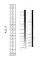
- FIG. 10 is a diagram showing a conventional pulse (drive voltage waveform) pattern of an applied voltage for one line.
- a conventional pulse drive voltage waveform
- a total of 31 pulses are applied to the electrodes from L1 which is the brightest gradation to L16 which is the darkest gradation.
- a time of 6110 ⁇ s which is the sum of the On and Off times of all 31 pulses.
- the number of lines to be scanned is assumed to be 1600. If the allowable time for rewriting one page is within 0.8 seconds, one line must be rewritten in 500 ⁇ sec or less.
- the conventional pulse pattern since it takes 6110 ⁇ sec to express 16 levels of gradation, only 5 gradations L1 to L5 can be expressed in 500 ⁇ sec. Further, in the conventional pulse pattern, since it is necessary to apply a total of 31 pulses in order to change the gradation from L1 to L16, there is a problem that the control of the applied voltage becomes complicated.
- an object of the present invention made in view of such a point is to provide an image display device capable of realizing a desired gradation with a small number of pulse applications and an application time.
- two types of particle groups having different charging characteristics are arranged between at least two substrates with electrodes whose viewing side screen area is transparent, and between the electrode pairs formed by facing the electrodes.
- a driving voltage is applied between the electrode pairs to drive the two types of particle groups.
- Drive voltage generating means wherein the drive voltage generating means expresses the gradation of the image by a combination of n drive voltage waveforms when the image to be displayed is displayed in 2 n tones. It is what.
- the n driving voltage waveform preferably has a time length corresponding to each value from 2 0 to 2 n-1.
- the time length T m of the driving voltage waveform corresponding to a value of 2 m is a driving voltage waveform corresponding to a value of 2 m ⁇ 1.
- a pulse pattern of a driving voltage for image formation is generated by combining n driving voltage waveforms. Can be realized in time.
- (A), (b) is a figure for demonstrating the example of the image display in the image display apparatus of this invention, respectively. It is a figure which shows an example of the pulse pattern in the image display apparatus of this invention. It is a figure which shows an example of the order change of the pulse to apply. It is a figure which shows an example of the pulse pattern containing offset time. It is a figure which shows a response
- (A), (b) is a figure which shows an example of a structure of the panel part in the image display apparatus of this invention, respectively.
- (A), (b) is a figure which shows the other example of a structure of the panel part in the image display apparatus of this invention, respectively. It is a figure which shows an example of the pulse pattern in the conventional image display apparatus.
- FIG. 1 is a conceptual diagram for explaining an example of an image display device of the present invention.
- the image display device of the present invention includes a panel unit 11 that is an image display unit and a drive voltage generation unit 21 for image formation.
- 1 is a lower first panel substrate
- 2 is an upper transparent second panel substrate
- 3W is a white particle group including negatively charged white particles 3Wa
- 3B is a black particle group including positively chargeable black particles 3Ba
- 5 is a first stripe electrode disposed on the first panel substrate 1
- 6 is a second panel substrate 2 having at least a transparent screen region. It is the transparent 2nd stripe electrode arrange
- the drive voltage generating means 21, 22 is a CPU
- 23 is a graphic controller for supplying an image to be displayed with an image forming drive voltage under the control of the CPU 22
- 24-1 is an image forming drive for the first stripe electrode 5.
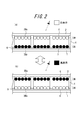
- FIGS. 2 (a) and 2 (b) are diagrams for explaining an example of image display on the panel unit of the image display device of the present invention.
- at least two kinds of particle groups in this case, including negatively charged white particles 3Wa
- the first stripe electrode 5 provided on the first panel substrate 1 in each cell formed by the ribs 4, showing the black particle group 3 ⁇ / b> B including the white particle group 3 ⁇ / b> W and the positively charged black particles 3 ⁇ / b> Ba).
- a transparent second stripe electrode 6 provided on the second panel substrate 2 having at least a transparent screen region, and an electric field generated by applying a voltage between the pair of pixel electrodes formed to cross each other at right angles.
- the substrate 1 and 2 are moved vertically.
- the white particle group 3W is visually recognized by the observer as shown in FIG. 2 (a), or the white display is displayed, or the black particle group 3B is visually recognized by the observer as shown in FIG. 2 (b). Is displayed in a matrix with black and white dots.
- the rib on the front side is omitted.
- an example is shown in which cells and pixels (dots) correspond one-to-one.
- 9 is an adhesive.
- the screen region of the second panel substrate 1 and the second stripe electrode 6 need to be transparent, but the first panel substrate 5 and the first stripe electrode 5 may be transparent or opaque. It is preferable that the space between the substrates in the region where the particle group is arranged has a sealing structure to prevent moisture from entering from the outside environment. It is preferable to form the sealing structure using an adhesive or sealing material having a high moisture barrier property.
- the driving voltage generating means 21 when displaying 2 n gradations, at least 2 n pulses are required in advance, but the driving voltage generating means 21 according to the present invention has 2 n power levels.
- a display of each gradation is realized by a combination of n pulses (drive voltage waveforms). That is, the drive voltage generation means 21 according to the present invention can express a desired gradation by applying a pulse n times at most.
- the drive voltage generation means 21 has a length corresponding to each value of 2 n ⁇ 1 , 2 n ⁇ 2 ,..., 2 2 , 2 1 , 2 0 when displaying 2 n gradations.
- a pulse pattern of the image forming drive voltage is generated by combining the pulses (P n ⁇ 1 , P n ⁇ 2 ,..., P 2 , P 1 , P 0 ).
- 2 n pulse patterns can be generated by combining n pulses.
- the length of the pulse P m (0 ⁇ m ⁇ n -1) the application time of the T m
- the application of the T m and, P m-1 and P m + 1 is a front and rear pulse of the pulse P m
- the relationship between the time lengths T m ⁇ 1 and T m + 1 can be defined as the following equations (1) and (2).
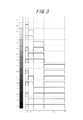
- FIG. 3 shows a pulse of the image forming drive voltage applied to the first stripe electrode 5 and the second stripe electrode 6 by the drive voltage generation means 21 in the case of 16 gradations (2 to the 4th power) of L1 to L16. It is a figure which shows an example of a pattern.
- Drive voltage generating means 21 when displaying a gradation of 2 4, 2 3, 2 2, 2 1, 2 0 of 4 pulses with a length corresponding to each value (P 3, P 2, P 1 , P 0 ) to generate a pulse pattern of the image forming drive voltage.
- the drive voltage generation means 21 when displaying the gradation of L12, the drive voltage generation means 21 generates a pulse pattern in which P 0 , P 1 and P 3 are combined.
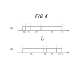
- the order of the four pulses can be changed for each line or each pixel (dot).
- the order of pulses to be applied can be the order shown in FIG. 4A
- the order of pulses to be applied can be the order shown in FIG. 4B.
- the time of P O 30 .mu.sec, 60 .mu.sec time P 1, 120 ⁇ sec time P 2 by setting the 240 ⁇ sec the time P 3, the total length of time from P1 P4 is next 450Myusec, 1 single A line can be drawn with 16 gradations within 500 ⁇ sec. In this time setting, a multiple of 2 of the time length of PO is simply used.
- FIG. 5 is a diagram illustrating an example of a pulse pattern including an offset time.
- the offset time Po 3 is set before the pulse P 3
- the offset time Po 0 is set after the pulse P 0 .
- before and after the offset time of the pulse P 2 is zero
- before and after the pulse P 1 is offset time Po 1_1 and Po 1_2 are set.
- the offset time may be set either before or after the pulse, and may be set both before and after the pulse.
- the offset time can be set to the same value for all pulses, or can be changed for each pulse, and an arbitrary value including zero can be set.
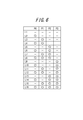
- FIG. 6 is a diagram showing combinations of pulses P 0 to P 3 for the respective gradations L1 to L16. As shown in FIGS. 3 and 6, the drive voltage generation means 21 can express an image of 16 gradations by applying a pulse four times at the maximum.
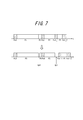
- FIG. 7 is a diagram illustrating an example of a pulse pattern including an off time.
- the offset time O P0 is set between the pulse P 3 and the pulse P
- offset time O P1 is set between the offset time Po 1_1 pulse P 2 and the pulse P 1.
- the off time between pulses can be set to the same value for all pulses or can be changed for each pulse, and can be set to any value including zero.
- the application range of the present invention is not limited to an image in the case of 16 gradations (2 to the 4th power). For example, 256 gradations (2 to the 8th power), 65536 gradations (2 to the 16th power), etc. It can cope with various gradations.
- Drive voltage generating means 21 when displaying a gradation of 2 8, 2 7-8 pulses (P 7 ⁇ P 0) by combining the driving for image formation having a length corresponding to each value of the 2 0 generates a pulse pattern of the voltage, when displaying a gradation of 2 16, 2 15-16 pulses (P 15 ⁇ P 0) for a combination of image formation having a length corresponding to each value of the 2 0 A pulse pattern of the driving voltage is generated.
- a pulse pattern of the image forming drive voltage is generated by combining n pulses (drive voltage waveform).
- the tone can be realized with a small number of pulse applications and application time. That is, when displaying 2n gradations, it is only necessary to apply a pulse at most n times, so that the applied voltage can be easily controlled. In addition, as the number of times of application decreases, it is possible to extend the life of the drive circuit, the panel, the electrode, and the like.
- n pulses have time lengths corresponding to the values 2 n ⁇ 1 , 2 n ⁇ 2 ,..., 2 2 , 2 1 , 2 0 , the combination of each pulse has the same value It becomes possible to prevent becoming.
- the formula (1) and (2) as in by defining the length of time between the front and rear pulses, 2 for n pulses n-1, 2 n-2, ⁇ ⁇ ⁇ , 2 2 It becomes possible to set the time length corresponding to each value of 2 1 , 2 0 with certainty.
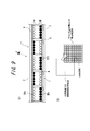
- FIGS. 8A, 8B, 9A, and 9B are diagrams showing other examples of the configuration of the panel section in the image display device of the present invention.
- the same members as those in the examples shown in FIGS. 2A and 2B are denoted by the same reference numerals. Description is omitted.
- FIGS. 8A, 8B, 9A, and 9B are diagrams showing other examples of the configuration of the panel section in the image display device of the present invention.
- the same members as those in the examples shown in FIGS. 2A and 2B are denoted by the same reference numerals. Description is omitted.
- FIG. 2 shows a part of the panel portion having this configuration. In the example shown in FIGS.
- An example of a dot matrix type active drive panel in which white particle groups 3W including negatively charged white particles 3Wa are enclosed is shown.
- the rear side substrate is a TFT substrate
- the observation side substrate is a common electrode substrate
- two types of particle groups arranged in each cell can be actively controlled by the TFT.
- the image display device of the present invention includes a notebook computer, an electronic notebook, a portable information device called PDA (Personal Digital Assistants), a display unit of a mobile device such as a mobile phone and a handy terminal, an electronic paper such as an electronic book and an electronic newspaper, Billboards such as signboards, posters, blackboards (whiteboards), electronic desk calculators, home appliances, automotive supplies, card displays such as point cards, IC cards, electronic advertisements, information boards, electronic POPs (Point Of Presence) , Point Of Purchase advertising), electronic price tag, electronic shelf label, electronic score, display part of RF-ID equipment, as well as display part of various electronic equipment such as POS terminal, car navigation device, watch, etc.
- PDA Personal Digital Assistants
- PDA Personal Digital Assistants
- a display unit of a mobile device such as a mobile phone and a handy terminal
- an electronic paper such as an electronic book and an electronic newspaper
- Billboards such as signboards, posters, blackboards (whiteboards)
- electronic desk calculators
- a display unit rewritable paper
- an external rewritable unit performs display rewriting.
- It is particularly suitable as an image display device having a panel portion having a display memory property for displaying an image by moving a child in a gas or in a vacuum.
- a dynamic drive method and a segment drive method can be applied to the drive method of the image display apparatus of the present invention.
Landscapes
- Engineering & Computer Science (AREA)
- Physics & Mathematics (AREA)
- Computer Hardware Design (AREA)
- General Physics & Mathematics (AREA)
- Theoretical Computer Science (AREA)
- Electrochromic Elements, Electrophoresis, Or Variable Reflection Or Absorption Elements (AREA)
- Control Of Indicators Other Than Cathode Ray Tubes (AREA)
Abstract
薄型の画像表示装置を提供する。本発明に係る画像表示装置は、少なくとも観察側画面領域が透明な2枚の電極付き基板間に、帯電特性の異なる2種類の粒子群を配置し、前記電極が対向して形成する電極対間に形成した電界で、前記2種類の粒子群をそれぞれ別の基板側に移動させて画像を表示する画像表示装置において、前記電極対間に駆動電圧を印加して前記2種類の粒子群を駆動させる駆動電圧生成手段を備え、該駆動電圧生成手段は、表示する画像を2のn乗の階調で表示する場合、n個の駆動電圧波形の組み合わせにより前記画像の階調を表現することを特徴とする。
Description
本発明は、画像表示装置に関するものである。
従来、少なくとも一方が透明な電極を配した基板ともう一方の電極を配した基板との対向空間に、帯電性粒子を含んだ粒子群として構成した表示媒体を封入し、表示させる画像に対応した電圧を電極に印加して、電極対間に発生させた電界により表示媒体を移動させて画像を表示する画像表示装置が知られている(例えば、特許文献1~3参照)。
図10は、1つのラインに対する印加電圧の従来のパルス(駆動電圧波形)パターンを示す図である。従来のパルスパターンで16段階の階調を変化させる場合、最も明るい階調であるL1から最も暗い階調であるL16に到達するまで、合計で31個のパルスが電極に加えられることになる。
従来のパルスパターンでは、1つのラインの画素の階調をL1からL16まで変化させるために、全31個のパルスのOn及びOff時間の合計である6110μ秒の時間が必要となる。例えば、13インチのパネルサイズを想定し、スキャンすべきライン本数を1600本と仮定する。1枚のページ書き換えに許容できる時間を0.8秒以内とすると、1つのラインの書き換えは500μ秒以下で行わなければならない。しかし、従来のパルスパターンでは、16段階の階調を表現するために6110μ秒の時間がかかるため、500μ秒では、L1~L5の5階調程度しか表現することが出来ない。また、従来のパルスパターンでは、L1からL16まで階調を変化させるために合計で31個のパルスを印加する必要があるため、印加電圧の制御が複雑になるという問題があった。
したがって、かかる点に鑑みてなされた本発明の目的は、所望の階調を少ないパルス印加回数及び印加時間で実現可能な画像表示装置を提供することにある。
本発明の画像表示装置は、少なくとも観察側画面領域が透明な2枚の電極付き基板間に、帯電特性の異なる2種類の粒子群を配置し、前記電極が対向して形成する電極対間に形成した電界で、前記2種類の粒子群をそれぞれ別の基板側に移動させて画像を表示する画像表示装置において、前記電極対間に駆動電圧を印加して前記2種類の粒子群を駆動させる駆動電圧生成手段を備え、該駆動電圧生成手段は、表示する画像を2のn乗の階調で表示する場合、n個の駆動電圧波形の組み合わせにより前記画像の階調を表現することを特徴とするものである。
また、前記n個の駆動電圧波形は、それぞれ、20から2n-1までの各値に対応した時間長をもつことが好ましい。
また、前記n個の駆動電圧波形のうち、2m(0≦m≦n-1)の値に対応した駆動電圧波形の時間長Tmは、2m-1の値に対応した駆動電圧波形の時間長Tm-1又は2m+1の値に対応した駆動電圧波形の時間長Tm+1との間で、下記式(1)又は式(2)
Tm≧2×Tm-1 式(1)
Tm≦(Tm+1)/2 式(2)
のいずれかを満たすことが好ましい。
Tm≧2×Tm-1 式(1)
Tm≦(Tm+1)/2 式(2)
のいずれかを満たすことが好ましい。
本発明によれば、2nの階調を表示する場合、n個の駆動電圧波形を組み合わせて画像形成用の駆動電圧のパルスパターンを生成するため、所望の階調を少ないパルス印加回数及び印加時間で実現することができる。
図1は本発明の画像表示装置の一例を説明するための概念図である。図1に示す例において、本発明の画像表示装置は、画像表示部であるパネル部11、画像形成用の駆動電圧生成手段21を含んで構成されている。
図1に示すパネル部11において、1は下側の第1のパネル基板、2は上側の透明な第2のパネル基板、3Wは負帯電性白色粒子3Waを含んで構成される白色粒子群、3Bは正帯電性黒色粒子3Baを含んで構成される黒色粒子群、5は第1のパネル基板1上に配置した第1のストライプ電極、6は少なくとも画面領域が透明な第2のパネル基板2上に配置した透明な第2のストライプ電極である。また、図1に示す駆動電圧生成手段21は、第1のストライプ電極5と第2のストライプ電極との電極対間に駆動電圧を印加して白色粒子群3Wと黒色粒子群3Bとを駆動させるものである。駆動電圧生成手段21において、22はCPU、23はCPU22の制御のもと画像形成用駆動電圧により表示すべき画像を供給するグラフィックコントローラ、24-1は第1のストライプ電極5に画像形成用駆動電圧を供給する第1のドライバIC、24-2は透明な第2のストライプ電極6に画像形成用駆動電圧を供給する第2のドライバICである。
図2(a)、(b)はそれぞれ本発明の画像表示装置のパネル部における画像表示の例を説明するための図である。図2(a)、(b)に示す例において、少なくとも光学的反射率および帯電性を有する粒子を含んで構成した少なくとも2種類の粒子群(ここでは負帯電性白色粒子3Waを含んで構成した白色粒子群3Wと正帯電性黒色粒子3Baを含んで構成した黒色粒子群3Bを示す)を、リブ4で形成された各セルにおいて、第1のパネル基板1に設けた第1のストライプ電極5と少なくとも画面領域が透明な第2のパネル基板2に設けた透明な第2のストライプ電極6とが対向直交交差して形成する画素電極対の間に電圧を印加することにより発生する電界に応じて、基板1、2と垂直に移動させる。そして、図2(a)に示すように白色粒子群3Wを観察者に視認させて白色の表示を、あるいは、図2(b)に示すように黒色粒子群3Bを観察者に視認させて黒色の表示を白黒のドットでマトリックス表示している。なお、図2(a)、(b)において、手前にあるリブは省略している。また、ここではセルと画素(ドット)とが1対1に対応する例を示している。さらに、9は接着剤である。本発明では、第2のパネル基板1の少なくとも画面領域および第2のストライプ電極6は透明である必要があるが、第1のパネル基板5および第1のストライプ電極5は透明でも不透明でも良い。粒子群を配置した領域の基板間の空間は封止構造とし、外部環境からの湿分進入を防止するのが好ましい。水分バリア性の高い接着剤やシール材を用いて封止構造を形成するのが好ましい。
一般的に、2のn乗の階調を表示する場合には、予め少なくとも2のn乗個のパルスが必要となるが、本発明に係る駆動電圧生成手段21は、2のn乗の階調を表示する場合、n個のパルス(駆動電圧波形)の組み合わせによって、各階調の表示を実現するものである。即ち、本発明に係る駆動電圧生成手段21は、最大でn回パルスを印加することにより、所望の階調を表現することが可能となる。駆動電圧生成手段21は、2nの階調を表示する場合、2n-1、2n-2、・・・、22、21、20という各値に対応した長さを持つn個のパルス(Pn-1、Pn-2、・・・、P2、P1、P0)を組み合わせて画像形成用駆動電圧のパルスパターンを生成する。n個のパルスそれぞれのONとOFFを考えると、n個のパルスを組み合わせることにより、2n通りのパルスパターンを生成することが出来る。ここで、パルスPm(0≦m≦n-1)の印加時間の長さをTmとすると、当該Tmと、パルスPmの前後のパルスであるPm-1及びPm+1の印加時間の長さTm-1及びTm+1との関係は、下記の式(1)、(2)のように規定できる。
Tm≧2×Tm-1 (1)
Tm≦(Tm+1)/2 (2)
Tm≧2×Tm-1 (1)
Tm≦(Tm+1)/2 (2)
図3は、L1~L16の16階調(2の4乗)の場合の、駆動電圧生成手段21が第1のストライプ電極5及び第2のストライプ電極6に印加する画像形成用駆動電圧のパルスパターンの一例を示す図である。駆動電圧生成手段21は、24の階調を表示する場合、23、22、21、20という各値に対応した長さを持つ4個のパルス(P3、P2、P1、P0)を組み合わせて画像形成用駆動電圧のパルスパターンを生成する。例えば、L12の階調を表示する場合、駆動電圧生成手段21は、P0、P1及びP3を組み合わせたパルスパターンを生成する。なお、4個のパルスの順番はライン毎や画素(ドット)毎に入れ替えることができる。例えば、あるラインでは印加するパルスの順番を図4(a)の順番とし、次のラインでは印加するパルスの順番を図4(b)の順番とすることができる。また、例えば、POの時間を30μsec、P1の時間を60μsec、P2の時間を120μsec、P3の時間を240μsecと設定すれば、P1からP4の時間長の合計は450μsecとなり、1つのラインを500μsec以内に16階調で描画することが可能となる。なお、この時間設定では単純にPOの時間長の2の倍数を用いたが、各パルスの立ち上り及び立ち下り等を考慮して、各パルスの前後にオフセット時間を含ませてもよい。例えば、図5はオフセット時間を含むパルスパターンの一例を示す図である。図5では、パルスP3の前にオフセット時間Po3が設定され、パルスP0の後にオフセット時間Po0が設定されている。また、パルスP2の前後のオフセット時間はゼロであり、パルスP1の前後にはオフセット時間Po1_1とPo1_2がそれぞれ設定されている。図5に示すとおり、オフセット時間はパルスの前後どちらに設定しても良く、前後両方に設定することも可能である。また、オフセット時間は、全パルスに対して同じ値を設定したり、パルス毎に値を変えることも可能であり、ゼロを含む任意の値を設定することができる。即ち、式(1)又は式(2)のいずれかを満たす範囲であれば、適宜各パルスの時間を変更させることができることに留意されたい。図6は、各階調L1~L16に対するパルスP0~P3の組み合わせを示す図である。図3及び図6に示すとおり、駆動電圧生成手段21は、最大で4回パルスを印加することにより、16階調の画像を表現することが出来る。
なお、各パルスは必ずしも連続的に印加する必要はなく、パルスの切換処理時間や消費電力等を考慮して、各パルスの間にパルスを印加しない時間(Off時間)を設定することもできる。例えば、図7はOff時間を含むパルスパターンの一例を示す図である。図7では、パルスP3とパルスP0との間にオフセット時間OP0が設定され、パルスP2とパルスP1のオフセット時間Po1_1との間にオフセット時間OP1が設定されている。パルス間のOff時間は、全パルスに対して同じ値を設定したり、パルス毎に値を変えることも可能であり、ゼロを含む任意の値を設定することができる。
なお、本発明の適用範囲は16階調(2の4乗)の場合の画像に限られるものではなく、例えば256階調(2の8乗)、65536階調(2の16乗)など、種々の階調に対応可能なものである。駆動電圧生成手段21は、28の階調を表示する場合、27~20の各値に対応した長さを持つ8個のパルス(P7~P0)を組み合わせて画像形成用駆動電圧のパルスパターンを生成し、216の階調を表示する場合、215~20の各値に対応した長さを持つ16個のパルス(P15~P0)を組み合わせて画像形成用駆動電圧のパルスパターンを生成する。
上述した本発明の画像表示装置によれば、2nの階調を表示する場合、n個のパルス(駆動電圧波形)を組み合わせて画像形成用駆動電圧のパルスパターンを生成するため、所望の階調を少ないパルス印加回数及び印加時間で実現することができる。即ち、2nの階調を表示する場合、最大n回だけパルスを印加すればよいため、印加電圧の制御を容易に行えるようになる。また、印加回数の減少に伴い、駆動回路、パネル、電極等の寿命を延ばすことが可能となる。
また、n個のパルスは、2n-1、2n-2、・・・、22、21、20という各値に対応した時間長を持つため、各パルスの組み合わせが同一の値となることを防ぐことが可能となる。また、式(1)及び(2)のように、前後のパルス間の時間長を規定することにより、n個のパルスに対して2n-1、2n-2、・・・、22、21、20という各値に対応した時間長を確実に設定することが可能となる。
次に、本発明の画像表示装置におけるパネル部の構成の他の例を説明する。図8(a)、(b)および図9(a)、(b)はそれぞれ本発明の画像表示装置におけるパネル部の構成の他の例を示す図である。図8(a)、(b)および図9(a)、(b)に示す例において、図2(a)、(b)に示す例と同一の部材には同一の符号を付し、その説明を省略する。図8(a)、(b)に示す例では、パネル部11として、隔壁4で囲まれた基板1、2間のセル空間内に、正帯電性黒色粒子3Baを含んだ黒色粒子群3Bおよび負帯電性白色粒子3Waを含んだ白色粒子群3Wを封入したドットマトリックス型パッシブ駆動パネルの例を示している。この構成のパネル部の一部を示したのが前述した図2である。図9(a)、(b)に示す例では、パネル部11として、隔壁4で囲まれた基板1、2間のセル空間内に、正帯電性黒色粒子3Baを含んだ黒色粒子群3Bおよび負帯電性白色粒子3Waを含んだ白色粒子群3Wを封入したドットマトリックス型アクティブ駆動パネルの例を示している。背面側基板をTFT基板とし、観察側基板を共通電極基板とし、各セルに配置した2種類の粒子群をTFTでアクティブ制御できる。
本発明の画像表示装置は、ノートパソコン、電子手帳、PDA(Personal Digital Assistants)と呼ばれる携帯型情報機器、携帯電話、ハンディターミナル等のモバイル機器の表示部、電子書籍、電子新聞等の電子ペーパー、看板、ポスター、黒板(ホワイトボード)等の掲示板、電子卓上計算機、家電製品、自動車用品等の表示部、ポイントカード、ICカード等のカード表示部、電子広告、情報ボード、電子POP(Point Of Presence, Point Of Purchase advertising)、電子値札、電子棚札、電子楽譜、RF-ID機器の表示部のほか、POS端末、カーナビゲーション装置、時計など様々な電子機器の表示部に好適に用いられるほか、外部書換え手段に接続して表示書き換えを行う表示部(リライタブルペーパー)としても好適に用いられるものであり、帯電性粒子を気体中または真空中で移動させて画像表示を行う表示メモリー性を有するパネル部を有する画像表示装置として、特に好適である。
本発明の画像表示装置の駆動方式には、パッシブ駆動方式、アクティブ駆動方式の他、ダイナミック駆動方式やセグメント駆動方式を適用できる。
本発明の画像表示装置の駆動方式には、パッシブ駆動方式、アクティブ駆動方式の他、ダイナミック駆動方式やセグメント駆動方式を適用できる。
1 第1のパネル基板
2 第2のパネル基板
3W 白色粒子群
3Wa 負帯電性白色粒子
3B 黒色粒子群
3Ba 正帯電性黒色粒子
4 リブ
5 第1のストライプ電極
6 第2のストライプ電極
9 接着剤
11 パネル部
21 駆動電圧生成手段
22 CPU
23 グラフィックコントローラ
24-1 第1のドライバIC
24-2 第2のドライバIC
2 第2のパネル基板
3W 白色粒子群
3Wa 負帯電性白色粒子
3B 黒色粒子群
3Ba 正帯電性黒色粒子
4 リブ
5 第1のストライプ電極
6 第2のストライプ電極
9 接着剤
11 パネル部
21 駆動電圧生成手段
22 CPU
23 グラフィックコントローラ
24-1 第1のドライバIC
24-2 第2のドライバIC
Claims (3)
- 少なくとも観察側画面領域が透明な2枚の電極付き基板間に、帯電特性の異なる2種類の粒子群を配置し、前記電極が対向して形成する電極対間に形成した電界で、前記2種類の粒子群をそれぞれ別の基板側に移動させて画像を表示する画像表示装置において、前記電極対間に駆動電圧を印加して前記2種類の粒子群を駆動させる駆動電圧生成手段を備え、該駆動電圧生成手段は、表示する画像を2のn乗の階調で表示する場合、n個の駆動電圧波形の組み合わせにより前記画像の階調を表現することを特徴とする画像表示装置。
- 前記n個の駆動電圧波形は、それぞれ、20から2n-1までの各値に対応した時間長をもつことを特徴とする請求項1に記載の画像表示装置。
- 前記n個の駆動電圧波形のうち、2m(0≦m≦n-1)の値に対応した駆動電圧波形の時間長Tmは、2m-1の値に対応した駆動電圧波形の時間長Tm-1又は2m+1の値に対応した駆動電圧波形の時間長Tm+1との間で、下記式(1)又は式(2)
Tm≧2×Tm-1 式(1)
Tm≦(Tm+1)/2 式(2)
のいずれかを満たすことを特徴とする、請求項2に記載の画像表示装置。
Applications Claiming Priority (2)
| Application Number | Priority Date | Filing Date | Title |
|---|---|---|---|
| JP2010-167214 | 2010-07-26 | ||
| JP2010167214A JP2012027319A (ja) | 2010-07-26 | 2010-07-26 | 画像表示装置 |
Publications (1)
| Publication Number | Publication Date |
|---|---|
| WO2012014434A1 true WO2012014434A1 (ja) | 2012-02-02 |
Family
ID=45529667
Family Applications (1)
| Application Number | Title | Priority Date | Filing Date |
|---|---|---|---|
| PCT/JP2011/004178 Ceased WO2012014434A1 (ja) | 2010-07-26 | 2011-07-25 | 画像表示装置 |
Country Status (2)
| Country | Link |
|---|---|
| JP (1) | JP2012027319A (ja) |
| WO (1) | WO2012014434A1 (ja) |
Citations (2)
| Publication number | Priority date | Publication date | Assignee | Title |
|---|---|---|---|---|
| JP2003315848A (ja) * | 2002-02-21 | 2003-11-06 | Bridgestone Corp | 画像表示装置 |
| JP2004102055A (ja) * | 2002-09-11 | 2004-04-02 | Seiko Epson Corp | 分散系駆動回路の駆動方法、分散系駆動回路、電気泳動表示装置の駆動方法、電気泳動表示装置及び電子機器 |
-
2010
- 2010-07-26 JP JP2010167214A patent/JP2012027319A/ja active Pending
-
2011
- 2011-07-25 WO PCT/JP2011/004178 patent/WO2012014434A1/ja not_active Ceased
Patent Citations (2)
| Publication number | Priority date | Publication date | Assignee | Title |
|---|---|---|---|---|
| JP2003315848A (ja) * | 2002-02-21 | 2003-11-06 | Bridgestone Corp | 画像表示装置 |
| JP2004102055A (ja) * | 2002-09-11 | 2004-04-02 | Seiko Epson Corp | 分散系駆動回路の駆動方法、分散系駆動回路、電気泳動表示装置の駆動方法、電気泳動表示装置及び電子機器 |
Also Published As
| Publication number | Publication date |
|---|---|
| JP2012027319A (ja) | 2012-02-09 |
Similar Documents
| Publication | Publication Date | Title |
|---|---|---|
| CN101840666B (zh) | 电泳显示装置、电子设备以及电泳显示面板的驱动方法 | |
| CN107886910A (zh) | 显示装置 | |
| JP2962985B2 (ja) | 液晶表示装置 | |
| CN101840123A (zh) | 电泳显示装置、电子设备以及电泳显示面板的驱动方法 | |
| KR20100023418A (ko) | 타이밍 제어장치 및 이를 갖는 표시장치 | |
| US20070057906A1 (en) | Bi-stable display with reduced memory requirement | |
| JP2009134354A (ja) | 情報表示装置 | |
| TWI477872B (zh) | 可顯示多灰階之顯示裝置及其操作方法 | |
| JPWO2009075356A1 (ja) | 情報表示用パネルの駆動方法および情報表示用パネル | |
| US6657610B1 (en) | Liquid-crystal display device and method of driving the same | |
| US8982166B2 (en) | Display device and driving method thereof | |
| JP2012027319A (ja) | 画像表示装置 | |
| US20170017133A1 (en) | Electronic paper display device | |
| JP2007206266A (ja) | 電気泳動表示装置および電子機器 | |
| KR101480003B1 (ko) | 전기 영동 표시 장치의 구동 방법 | |
| JP2008158243A (ja) | 表示装置 | |
| JP2010107723A (ja) | 情報表示パネルのマザーパネル、その通電検査方法およびマザーパネルを用いて作製した情報表示パネル | |
| JP2010139863A (ja) | ドットマトリックス型ディスプレイパネル | |
| KR20060024942A (ko) | 구동유닛 및 이를 갖는 표시장치 | |
| JP2011158575A (ja) | 情報表示用パネル | |
| JP2010113154A (ja) | 情報表示装置の駆動方法 | |
| JP2009288600A (ja) | ドットマトリックス型情報表示用パネル | |
| KR200146987Y1 (ko) | 교류형 플라즈마 디스플레이의 구동장치 | |
| JP5115831B2 (ja) | 電気泳動表示装置、コントローラ、および電子機器 | |
| JP5024461B2 (ja) | 電気泳動表示装置、電子機器、電気泳動表示装置の駆動方法、およびコントローラ |
Legal Events
| Date | Code | Title | Description |
|---|---|---|---|
| 121 | Ep: the epo has been informed by wipo that ep was designated in this application |
Ref document number: 11812036 Country of ref document: EP Kind code of ref document: A1 |
|
| NENP | Non-entry into the national phase |
Ref country code: DE |
|
| 122 | Ep: pct application non-entry in european phase |
Ref document number: 11812036 Country of ref document: EP Kind code of ref document: A1 |