WO2012014394A1 - 受信装置及び受信方法 - Google Patents
受信装置及び受信方法 Download PDFInfo
- Publication number
- WO2012014394A1 WO2012014394A1 PCT/JP2011/003972 JP2011003972W WO2012014394A1 WO 2012014394 A1 WO2012014394 A1 WO 2012014394A1 JP 2011003972 W JP2011003972 W JP 2011003972W WO 2012014394 A1 WO2012014394 A1 WO 2012014394A1
- Authority
- WO
- WIPO (PCT)
- Prior art keywords
- signal
- correction value
- temperature
- phase
- circuit
- Prior art date
- Legal status (The legal status is an assumption and is not a legal conclusion. Google has not performed a legal analysis and makes no representation as to the accuracy of the status listed.)
- Ceased
Links
Images






Classifications
-
- H—ELECTRICITY
- H04—ELECTRIC COMMUNICATION TECHNIQUE
- H04B—TRANSMISSION
- H04B1/00—Details of transmission systems, not covered by a single one of groups H04B3/00 - H04B13/00; Details of transmission systems not characterised by the medium used for transmission
- H04B1/06—Receivers
- H04B1/16—Circuits
- H04B1/30—Circuits for homodyne or synchrodyne receivers
-
- H—ELECTRICITY
- H04—ELECTRIC COMMUNICATION TECHNIQUE
- H04L—TRANSMISSION OF DIGITAL INFORMATION, e.g. TELEGRAPHIC COMMUNICATION
- H04L27/00—Modulated-carrier systems
- H04L27/32—Carrier systems characterised by combinations of two or more of the types covered by groups H04L27/02, H04L27/10, H04L27/18 or H04L27/26
- H04L27/34—Amplitude- and phase-modulated carrier systems, e.g. quadrature-amplitude modulated carrier systems
- H04L27/38—Demodulator circuits; Receiver circuits
Definitions
- the present disclosure relates to a receiving apparatus, and more particularly, to a technique for suppressing changes in image signal suppression characteristics due to temperature.
- a receiver that converts an RF (radio frequency) signal into an IF (intermediate frequency) signal by one frequency conversion has been actively developed. This is because an external filter such as a SAW filter is not necessary, and the wireless communication apparatus can be downsized.
- LOW-IF receiver has a problem of deterioration of reception sensitivity due to image signal.
- image signal and the desired signal to be received cannot be distinguished by power.
- image removal methods For example, it is generally performed to generate an I signal and a Q signal by multiplying a received signal by two signals orthogonal to each other to generate an I signal and a Q signal, and to attenuate only the image signal by an image suppression filter. .
- ( ⁇ A / A) and ⁇ are the amplitude error and phase error between the I signal and the Q signal.
- the amplitude error and the phase error from the ideal phase difference are between the I signal and the Q signal.
- IQ mismatch the image suppression ratio is reduced.
- An example of a correction method for reducing IQ mismatch is described in Patent Document 1.
- the phase and amplitude of the I signal and the Q signal are adjusted, and as a result, an image suppression ratio of, for example, 45 dB or more is realized.
- An object of the present invention is to perform correction with respect to the temperature change of the characteristics of each receiving apparatus as a whole in a shorter time.
- a receiving apparatus includes a quadrature signal generation unit that multiplies a reception signal by an in-phase local signal and a quadrature local signal that are substantially orthogonal to each other to generate an in-phase signal and a quadrature signal, and the quadrature signal.
- a storage circuit for storing a table indicating a relationship between the temperature and the correction value obtained by controlling the current supplied to the generation unit, and reading the table from the storage circuit and indicating the received temperature information
- a control circuit that selects a correction value corresponding to temperature from the table, and at least one of a relative amplitude and phase between the in-phase signal and the quadrature signal is changed according to the correction value, and after the change
- a signal adjustment circuit that outputs the in-phase signal and the changed quadrature signal, and outputs a component within a predetermined band of the changed in-phase signal and the changed quadrature signal.
- a filter circuit for storing a table indicating a relationship between the temperature and the correction value obtained by controlling the current supplied to the generation unit, and reading the table from the storage circuit and indicating the received temperature information
- a control circuit that selects a correction value corresponding to temperature from the table, and at least one of a relative amplitude and phase between the in-phase signal and the quadrature signal is changed according to the correction
- a reception method multiplies a reception signal by an in-phase local signal and a quadrature local signal that are substantially orthogonal to each other to generate an in-phase signal and a quadrature signal, and the in-phase signal and the quadrature signal,
- a table indicating the relationship between the temperature and the correction value obtained by controlling the current supplied to the quadrature signal generation unit that generates the data is stored in the storage circuit, and the table is read from the storage circuit and received.
- the correction value corresponding to the temperature indicated by the temperature information is selected from the table, and at least one of the relative amplitude and phase between the in-phase signal and the quadrature signal is read from the storage circuit.
- a component within a predetermined band is output from the changed in-phase signal and the changed quadrature signal.
- the correction of the characteristics is performed using the correction value obtained by controlling the current supplied to the quadrature signal generation unit without actually changing the temperature of the receiving device.
- the correction for the temperature change of the characteristics of each receiving apparatus can be performed in a shorter time.
- FIG. 1 is a block diagram illustrating a configuration example of a receiving apparatus according to an embodiment of the present invention.
- FIG. 2 is a block diagram illustrating a configuration example of the signal adjustment circuit of FIG.
- FIG. 3 is a spectrum diagram conceptually showing the relationship between the desired signal and the image signal.
- FIG. 4 is a graph showing an example of the relationship of gain to frequency in the receiving apparatus of FIG.
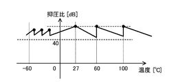
- FIG. 5 is a graph showing an example of the relationship between the temperature and the image suppression ratio when the amplitude and phase of the signal input to the filter circuit of FIG. 1 are not corrected.
- FIG. 6 is a flowchart illustrating an example of processing for generating and storing a table indicating the relationship between the temperature and the correction value in the receiving apparatus of FIG.
- FIG. 1 is a block diagram illustrating a configuration example of a receiving apparatus according to an embodiment of the present invention.
- FIG. 2 is a block diagram illustrating a configuration example of the signal adjustment circuit of FIG.
- FIG. 3 is a
- FIG. 7 is a diagram showing an example of the relationship between the temperature and the output current value of the variable current source of FIG. 1 in which an IQ mismatch corresponding to the temperature occurs.
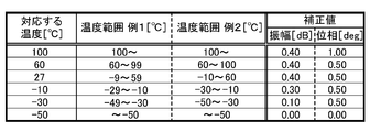
- FIG. 8 is a table showing an example of the relationship between the temperature obtained by the process of FIG. 6 and the correction value.
- FIG. 9 is a flowchart illustrating an example of processing during a reception operation of the reception apparatus in FIG.
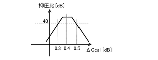
- FIG. 10 is a graph showing an example of the relationship between the amplitude correction value ⁇ Gcal and the image suppression ratio of the receiving apparatus of FIG. 1 at 27 ° C.
- FIG. 11 is a graph showing an example of the relationship between the amplitude correction value ⁇ Gcal and the image suppression ratio of the receiving apparatus of FIG. 1 at 100 ° C.
- FIG. 12 is a graph showing an example of the relationship between the temperature and the image suppression ratio in the receiving apparatus of FIG. 1 obtained by the process of FIG.
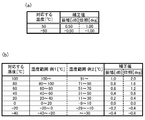
- FIG. 13A is an example of a table having correction values at two temperatures.
- FIG. 13B is an example of a table having correction values obtained by interpolation from FIG.
- FIG. 14 is a flowchart showing a modified example of the process of FIG.
- FIG. 15 is another example of the table of FIG.
- FIG. 16 is a flowchart showing another modification of the process of FIG.
- FIG. 1 is a block diagram showing a configuration example of a receiving apparatus according to an embodiment of the present invention.
- 1 includes a bandpass filter (BPF) 14, a low noise amplifier 16, an orthogonal signal generation unit 20, a signal adjustment circuit 40, a filter circuit 52, a measurement circuit 54, a demodulation circuit 56, and the like.
- BPF bandpass filter
- the orthogonal signal generation unit 20 includes a first mixer unit 21, a second mixer unit 31, a local signal generator 36, and a frequency divider 38.
- the first mixer unit 21 includes a local signal amplifier 22, a mixer 23, and an IF amplifier 24.
- the second mixer unit 31 includes a local signal amplifier 32, a mixer 33, and an IF amplifier 34.
- the local signal amplifier 22 and the local signal amplifier 32 are configured similarly and have the same gain.
- the mixer 23 and the mixer 33 are configured similarly and have the same gain.
- the IF amplifier 24 and the IF amplifier 34 are configured similarly and have the same gain.
- the antenna 12 receives a radio signal and supplies the received signal to the BPF 14.
- the BPF 14 passes only the necessary band components of the received signal.
- the low noise amplifier 16 amplifies the signal output from the BPF 14 and outputs the obtained signal ARF.
- the local signal generator 36 generates a local signal.
- the frequency divider 38 divides the local signal to generate an in-phase local signal I_LO1 and a quadrature local signal Q_LO1 that have a frequency half that of the local signal and are substantially orthogonal to each other.
- the local signal amplifier 22 amplifies the signal I_LO ⁇ b> 1 and outputs the amplified signal I_LO to the mixer 23.
- the local signal amplifier 32 amplifies the signal Q_LO 1 and outputs the amplified signal Q_LO to the mixer 33.
- the mixer 23 multiplies the signal ARF by the in-phase local signal I_LO to generate and output the down-converted in-phase signal I_IF1.
- the mixer 33 multiplies the signal ARF by the orthogonal local signal Q_LO to generate and output a down-converted orthogonal signal Q_IF1.
- the IF amplifier 24 amplifies the signal I_IF1 to generate and output an in-phase signal I_IF.
- the IF amplifier 34 amplifies the signal Q_IF1 to generate a quadrature signal Q_IF and outputs it.
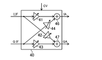
- FIG. 2 is a block diagram showing a configuration example of the signal adjustment circuit 40 of FIG.
- the signal adjustment circuit 40 includes amplifiers 41, 42, 43, 44 and adders 46, 47.
- the amplifiers 41 to 44 amplify the signals input thereto with a gain corresponding to the correction value CV and output the amplified signals.
- the adder 46 adds the outputs of the amplifier 41 and the amplifier 44 and outputs the result as a signal IA.
- the adder 47 adds the outputs of the amplifier 42 and the amplifier 43, and outputs the result as a signal QA.
- the amplitude of the signal IA can be changed by setting only the gain of the amplifier 41 or the gains of the amplifier 41 and the amplifier 44 to appropriate values according to the correction value CV. Since the signal I_IF and the signal Q_IF have a phase difference of 90 °, the phase of the signal IA can be changed by setting the gains of the amplifier 41 and the amplifier 44 to appropriate values according to the correction value CV. Both the amplitude and phase of the signal IA may be changed. Similarly, either or both of the amplitude and the phase of the signal QA can be changed by setting the gains of the amplifier 42 and the amplifier 43 to appropriate values according to the correction value CV.
- the signal adjustment circuit 40 changes at least one of the relative amplitude and phase between the in-phase signal I_IF and the quadrature signal Q_IF according to the set correction value CV, and changes the in-phase after the change.
- the signal IA and the changed quadrature signal QA are output.
- the correction value indicates at least one of an amplitude correction value and a phase correction value.
- FIG. 2 shows as an example the signal adjustment circuit 40 that changes the amplitude and phase of the in-phase signal I_IF and the quadrature signal Q_IF using the four amplifiers 41 to 44 and the two adders 46 and 47.
- the circuit changes the relative amplitude or phase between the in-phase signal I_IF and the quadrature signal Q_IF, another circuit may be used as the signal adjustment circuit 40 instead of the circuit of FIG.
- the filter circuit 52 in FIG. 1 passes components in a predetermined band out of the in-phase signal IA and the quadrature signal QA and outputs them as the in-phase signal I and the quadrature signal Q.
- the measurement circuit 54 obtains the signal strengths of the in-phase signal I and the quadrature signal Q and outputs them to the control circuit 64.
- the signal strength for example, the power of these signals, that is, the sum of the square of the signal I and the square of the signal Q is obtained.
- the measurement circuit 54 may obtain the voltage of one of the signals I and Q or the average of both signals as the signal strength.
- the signal strength is obtained as an RSSI (received signal strength) indicator, for example.
- the demodulation circuit 56 performs appropriate demodulation processing on the in-phase signal I and the quadrature signal Q, and outputs the demodulation result to the outside of the receiving apparatus 100.
- the variable current source 68 supplies a power source current to the orthogonal signal generation unit 20 according to the control circuit 64. That is, the control circuit 64 controls the current supplied to the quadrature signal generation unit 20 by controlling the variable current source 68.
- the control circuit 64 obtains an appropriate correction value using the signal intensity obtained by the measurement circuit 54, and generates a table indicating the relationship between the temperature and the correction value.
- the storage circuit 62 stores this table.
- the temperature sensor 66 outputs temperature information indicating the temperature of the receiving device in FIG. 1 to the control circuit 64 as, for example, a voltage.
- the control circuit 64 reads a table indicating the relationship between the temperature and the correction value from the storage circuit 62, selects a correction value corresponding to the temperature indicated by the received temperature information from the table, and sets the correction value CV as the signal adjustment circuit 40. Output to.
- variable current source 68 may not be included in the receiving device of FIG. 1.
- a current similar to that of the variable current source 68 is supplied from the outside of the receiving device to the quadrature signal generator 20. To be supplied.
- the circuits to which current is supplied from the variable current source 68 or the like may be all circuits included in the orthogonal signal generation unit 20 or a part of the circuits.
- a current may be supplied from a variable current source 68 or the like to a circuit that is not included in the orthogonal signal generation unit 20.
- the receiving device may not have the temperature sensor 66 as long as the control circuit 64 can obtain temperature information.
- the control circuit 64 may use a value corresponding to a voltage value or a current value in a circuit constituting the receiving device in FIG. 1 as temperature information. Further, a voltage or value corresponding to temperature information may be supplied to the control circuit 64 from the outside of the receiving device.
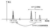
- FIG. 3 is a spectrum diagram conceptually showing the relationship between the desired signal and the image signal.
- signals of various frequencies are input to the antenna 12 in FIG. Since the BPF 14 is used for the purpose of suppressing unnecessary signals outside the system band, when a desired signal (frequency: f_RF) and an image signal (frequency: f_IM) as shown in FIG. However, the BPF 14 cannot suppress the image signal.
- the bandwidth of the BPF 14 is, for example, about several MHz to several hundred MHz.
- the frequency of the local signal is f_LO, f_RF> f_LO
- f_RF ⁇ f_LO f_LO ⁇ f_IM
- the filter circuit 52 As described with reference to FIG. 3, the desired signal and the image signal cannot be distinguished only by the power, but can be distinguished by using the phase. Therefore, in the receiving apparatus of FIG. 1, the signal input to the filter circuit 52 is divided into two orthogonal signals so that the desired signal and the image signal can be distinguished, and only the image signal is suppressed.
- the phase difference between the signal IA and the signal QA input to the filter circuit 52 is 90 degrees in an ideal state.
- the deviation from 90 degrees in the phase difference between the signal IA and the signal QA is referred to as a phase error between the signal IA and the signal QA
- the difference in amplitude between the signal IA and the signal QA is defined as the signal IA and the signal IA. This is referred to as an amplitude error between the signal QA.
- the phase error between the signal IA and the signal QA is 0.1 degrees or less and the amplitude error is 0.1 dB or less from the equation (A1). There is a need.
- the signal adjustment circuit 40 adjusts the amplitude and phase of the signal I_IF and the signal Q_IF according to the set value CV so that the signal IA and the signal QA satisfy this condition.
- the amplitude error and the phase error are referred to as IQ mismatch amount.
- the signal adjustment circuit 40 increases the amplitude of the signal I_IF by 1 dB when the amplitude of the signal I_IF is ⁇ 21 dBm and the amplitude of the signal Q_IF is ⁇ 20 dBm, for example.
- +1 dB is the amplitude correction value of the signal I_IF.
- ⁇ 1 dB is the amplitude correction value of the signal Q_IF.
- the signal I_IF may be corrected by +0.5 dB
- the signal Q_IF may be corrected by ⁇ 0.5 dB.
- the phase In the present embodiment, a case will be described in which an amplitude correction value and a phase correction value for the signal I_IF are given to the signal adjustment circuit 40 as a correction value CV.
- the amplitude and phase of the signal I and the signal Q which are output signals of the filter circuit 52 are measured, and the amplitude and the phase are compared between the signal I and the signal Q. It is only necessary to measure the IQ mismatch amount (amplitude error and phase error) to obtain the amplitude correction value and the phase correction value. However, obtaining the IQ mismatch amount by such a method is not realistic in view of the resolution of the measuring instrument used for the measurement and the labor required for the measurement.
- the magnitude of the signals I and Q output from the filter circuit is minimized.
- the amplitude correction value and the phase correction value are correction values to be obtained. Therefore, the control circuit 64 and the measurement circuit 54 obtain the power of these signals as signal strength.
- the amplitude correction value and the phase correction value are preferably digitized data, and the steps are optional.
- the amplitude correction value is a value of 0.1 dB step or 0.05 dB step
- the phase correction value is a value of 0.1 degree step or 0.05 degree step.
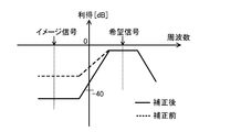
- FIG. 4 is a graph showing an example of the relationship of gain to frequency in the receiving apparatus of FIG.
- the difference between the gain of the image signal and the gain of the desired signal that is, the image suppression ratio
- the image suppression ratio can be 40 dB or more (solid line).
- the IQ mismatch value varies with temperature. This is because the characteristics of the circuit are affected by the temperature, and the amplitude and phase difference of the signal I_IF and the signal Q_IF change depending on the temperature.
- FIG. 5 is a graph showing an example of the relationship between the temperature and the image suppression ratio when the amplitude and phase of the signal input to the filter circuit 42 in FIG. 1 are not corrected. Since the IQ mismatch amount differs for each receiving device, it is necessary to set individual values for the phase correction value and the amplitude correction value for each receiving device. For this reason, it is necessary to obtain a correction value in a shipping process of an IC (integrated circuit), a module, or the receiving device that constitutes the receiving device.
- IC integrated circuit
- the correction value is obtained by setting the temperature of the receiving device to 27 ° C., and the correction value is set in the signal adjustment circuit 40. Then, the image suppression ratio at 27 ° C. of the receiving apparatus is 40 dB or more. However, as shown in FIG. 5, the image suppression ratio decreases as the temperature of the receiving apparatus is gradually increased. In this example, when the temperature of the receiving device is 100 ° C., the image suppression ratio is 40 dB or less. In this example, even if the temperature of the receiving device is ⁇ 60 ° C., the image suppression ratio is 40 dB or less.
- FIG. 6 is a flowchart showing an example of processing for generating and storing a table indicating the relationship between the temperature and the correction value in the receiving apparatus of FIG.
- the control circuit 64 obtains the relationship between the temperature and the correction value (for example, the phase correction value and the amplitude correction value) and stores it in the storage circuit 62. This processing is basically performed before the receiving device is shipped.
- an image signal is input from the outside to the receiving apparatus of FIG. Since it is difficult to directly input the image signal as a radio signal from the antenna, the image signal is input to the BPF 14 or the low noise amplifier 16 from the outside of the receiving apparatus using a coaxial cable. An image signal may be input to the mixers 23 and 33.
- the control circuit 64 determines whether or not there is an unmeasured condition.
- the measurement conditions are, for example, 27 ° C., 60 ° C., 100 ° C., ⁇ 10 ° C., ⁇ 30 ° C., and ⁇ 50 ° C. If there is an unmeasured condition, the process proceeds to 116. If not, the input of the image signal is stopped and the process of FIG. 6 is terminated.
- the variable current source 68 changes the output current value according to the instruction of the control circuit 64. For example, if the measurement condition is 60 ° C., the control circuit 64 sets the output current value of the variable current source 68 to a value that causes the same IQ mismatch as that at 60 ° C. At this time, the temperature of the receiving apparatus 100 in FIG. 1 is not actually changed.
- FIG. 7 is a diagram showing an example of the relationship between the temperature and the output current value of the variable current source 68 of FIG. 1 in which an IQ mismatch corresponding to the temperature occurs.
- the relationship between the temperature and the IQ mismatch and the relationship as shown in FIG. 7 are obtained in advance for the sampled reception circuit, and the obtained relationship is also used in the processing for a plurality of other reception circuits.
- the output current value of the variable current source 68 that causes an IQ mismatch corresponding to 60 ° C. is 1.1 times the output current value that causes an IQ mismatch corresponding to 27 ° C.
- the control circuit 64 changes the correction value CV set in the signal adjustment circuit 40, and obtains the correction value CV when the signal intensity measured by the measurement circuit 54 is the smallest.
- the measurement circuit 54 may obtain the signal intensity only for the signal I, and when the signal I is minimized, the signal Q is also minimized. Since it is not an essential problem whether the signal I or the signal Q is used, the simpler one may be used in terms of the configuration of the receiving apparatus.
- the setting value CV may be obtained for each of the signal I and the signal Q, and the average of the values for both signals may be obtained.
- control circuit 64 stores the obtained correction value CV in the storage circuit 62 in association with the temperature and the temperature range. Thereafter, the process returns to 114.
- the same treatment is performed for measurement conditions of 27 ° C., 100 ° C., ⁇ 10 ° C., ⁇ 30 ° C., and ⁇ 50 ° C., for example.
- FIG. 8 is a table showing an example of the relationship between the temperature obtained by the processing of FIG. 6 and the correction value.
- the control circuit 64 With the processing in FIG. 6, the control circuit 64 generates a table indicating the relationship between the temperature and the temperature range, the phase correction value, and the amplitude correction value as illustrated in FIG. 8 and stores the table in the storage circuit 62.
- the correction value corresponding to 27 ° C. indicates that the amplitude is 0.40 dB and the phase is 0.50 degrees.
- these correction values are used when the temperature range is ⁇ 9 to 59 ° C. (Example 1) or the temperature range is 0 to 39 ° C. (Example 2).
- the table of FIG. 8 for the receiving apparatus 100 can be obtained without actually changing the temperature of the receiving apparatus 100 of FIG.
- the temperature resolution is 1 ° C.
- FIG. 8 is an example, and another range may be set as the temperature range corresponding to the correction value. In the following description, it is assumed that the temperature range of Example 1 is set in the table of FIG.
- FIG. 8 shows an example in which the phase correction value and the amplitude correction value are obtained so that the signal intensity of the signal I is minimized.
- the storage circuit 62 may store only one of the phase correction value and the amplitude correction value.
- the control circuit 64 may obtain and store the phase correction value and the amplitude correction value so that the signal intensity of the signal Q instead of the signal I is minimized.
- the control circuit 64 may obtain and store a phase correction value and an amplitude correction value (that is, four correction values for each measurement condition) for each of the signal I and the signal Q.
- the correction value may be obtained at a narrower temperature interval or a wider temperature interval.
- the correction value may be obtained at a small number of temperatures.
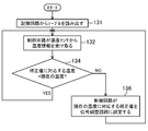
- FIG. 9 is a flowchart illustrating an example of processing during a reception operation of the reception apparatus in FIG.
- the control circuit 64 reads the table of FIG. 8 from the storage circuit 62.
- the control circuit 64 receives temperature information from the temperature sensor 66.
- the control circuit 64 receives temperature information indicating 27 ° C.
- the control circuit 64 determines whether or not the temperature corresponding to the correction value set in the signal adjustment circuit 40 (the leftmost column in FIG. 8) is equal to the current temperature. If equal, return to 132; otherwise, go to 136. Here, since it is immediately after the operation is started, the process proceeds to 136. In 136, the control circuit 64 sets a correction value corresponding to the current temperature in the signal adjustment circuit 40. Since the current temperature is 27 ° C., the control circuit 64 selects the amplitude correction value 0.40 dB and the phase correction value 0.50 degrees from the table of FIG. 8 and sets them in the signal adjustment circuit 40. Thereafter, the process returns to 132. Thereafter, the processes 132, 134 and 136 are repeated in the same manner.
- FIG. 10 is a graph showing an example of the relationship between the amplitude correction value ⁇ Gcal and the image suppression ratio of the receiving apparatus of FIG. 1 at 27 ° C. If the amplitude correction value set in the signal adjustment circuit 40 is 0, the value of the image suppression ratio will be 40 dB or less. However, since the amplitude correction value is set to 0.4 dB, the image suppression ratio is 40 dB. It is the above value. Since the phase correction value can be described in the same manner, the description of the phase correction value is omitted.
- the receiving apparatus can receive the desired signal without lowering the receiving sensitivity due to the influence of the image signal.
- FIG. 11 is a graph showing an example of the relationship between the amplitude correction value ⁇ Gcal and the image suppression ratio of the receiving apparatus of FIG. 1 at 100 ° C.
- the optimum amplitude correction value at 27 ° C. of the receiver of FIG. 1 was 0.40 dB, but as shown by the solid line in FIG. 11, the optimum amplitude correction value at 100 ° C. is 0.70 dB. is there.
- the control circuit 64 receives temperature information indicating 100 ° C. from the temperature sensor 66. In 134, the control circuit 64 determines whether or not the temperature 27 ° C. corresponding to the currently set correction value is equal to the current temperature 100 ° C. In this case, since it is not equal, it progresses to 136. In 136, the control circuit 64 sets a correction value corresponding to the current temperature in the signal adjustment circuit 40. Since the current temperature is 100 ° C., the control circuit 64 selects the amplitude correction value 0.70 dB and the phase correction value 2.00 degrees from the table of FIG. 8 and sets them in the signal adjustment circuit 40. Thereafter, the process returns to 132.
- the receiving apparatus of FIG. 1 changes the correction value even when the temperature rises to 100 ° C.
- the image suppression ratio can be ensured without being affected by the IQ mismatch temperature fluctuation. It becomes possible.
- the case where the amplitude correction value is changed has been described, but the phase correction value can also be changed similarly. Similarly, the correction value can be changed when the temperature of the receiving device is lowered.
- FIG. 12 is a graph showing an example of the relationship between the temperature and the image suppression ratio in the receiving apparatus of FIG. 1 obtained by the processing of FIG. Since the correction value is switched when the temperature of the receiving device becomes ⁇ 50 ° C., ⁇ 30 ° C., ⁇ 10 ° C., 60 ° C. and 100 ° C., the image in the range of about ⁇ 60 ° C. to 140 ° C. in the case of FIG.
- the suppression ratio can be kept at 40 dB or higher. Therefore, the receiving apparatus of FIG. 1 can receive a desired signal with almost no decrease in receiving sensitivity due to the influence of an image signal even if the temperature changes.
- FIG. 13A is an example of a table having correction values at two temperatures.
- FIG. 13B is an example of a table having correction values obtained by interpolation from FIG.
- the control circuit 64 obtains an amplitude correction value and a phase correction value at 50 ° C. and ⁇ 50 ° C. by the process of FIG.
- the control circuit 64 obtains another temperature correction value from the correction values at 50 ° C. and ⁇ 50 ° C.
- the control circuit 64 obtains correction values for other temperatures by linear interpolation.
- the difference between the two temperatures is 100 ° C.
- the correction value at 0 ° C. is 0.
- 50 + ( ⁇ 0.50) 0.00 dB
- the control circuit 64 performs amplitude correction values and phase correction values at, for example, 100 ° C., 80 ° C., 60 ° C., 40 ° C., 20 ° C., 0 ° C., ⁇ 20 ° C. and ⁇ 40 ° C. according to the equations (1) and (2). Ask for. As shown in FIG. 13B, the control circuit 64 causes the storage circuit 62 to store the obtained phase correction value and amplitude correction value in association with the temperature and the temperature range.
- correction values at 50 ° C. and ⁇ 50 ° C. are obtained by the processing of FIG. 6
- correction values at other temperatures may be obtained.
- the correction values obtained at the two temperatures by the process of FIG. 6 are used to interpolate the correction values at the other temperatures by the linear function
- the correction values may be obtained by another function.
- the correction values may be obtained at other intervals, or at non-constant intervals.
- a correction value may be obtained.
- the correction value is obtained by linear interpolation as shown in FIG.
- the correction value is obtained by the process of FIG. 6 at a smaller number of temperatures by interpolation using an optimal function. be able to.
- FIG. 14 is a flowchart showing a modification of the processing of FIG.
- FIG. 15 is another example of the table of FIG. Here, as an example, it is assumed that the table of FIG. 15 is obtained by the processing of FIG.
- the control circuit 64 reads the table of FIG.
- the control circuit 64 receives temperature information from the temperature sensor 66. For example, the control circuit 64 receives temperature information indicating 27 ° C.
- control circuit 64 determines whether or not the temperature corresponding to the current correction value set in the signal adjustment circuit 40 (the leftmost column in FIG. 15) is equal to the current temperature. If equal, return to 132; otherwise, go to 135. Here, since it is immediately after starting the operation, the process proceeds to 135.
- control circuit 64 determines whether or not the current correction value is equal to the correction value corresponding to the current temperature. If equal, return to 132; otherwise, go to 136. Here, since it is immediately after the operation is started, the process proceeds to 136.
- the control circuit 64 sets a correction value corresponding to the current temperature in the signal adjustment circuit 40. Since the current temperature is 27 ° C., the control circuit 64 selects the amplitude correction value 0.40 dB and the phase correction value 0.50 degrees from the table of FIG. 15 and sets them in the signal adjustment circuit 40. Thereafter, the process returns to 132.
- the control circuit 64 receives temperature information indicating 60 ° C. from the temperature sensor 66. In 134, the control circuit 64 determines whether the temperature 27 ° C. corresponding to the currently set correction value is equal to the current temperature 60 ° C. In this case, it is not equal, so go to 135.
- the control circuit 64 determines whether the current amplitude correction value 0.40 dB and the phase correction value 0.50 dB are equal to the amplitude correction value 0.40 dB and the phase correction value 0.50 dB corresponding to the current temperature. judge. In this case, since the two amplitude correction values are equal and the two phase correction values are equal, the process returns to 132. That is, the control circuit 64 does not change the correction value set in the signal adjustment circuit 40.
- the control circuit 64 receives temperature information indicating 100 ° C. from the temperature sensor 66. In 134, the control circuit 64 determines whether or not the temperature 60 ° C. corresponding to the currently set correction value is equal to the current temperature 100 ° C. In this case, it is not equal, so go to 135.
- control circuit 64 determines whether or not the current amplitude correction value 0.40 dB and the phase correction value 0.50 dB are equal to the amplitude correction value 0.40 dB and the phase correction value 1.00 dB corresponding to the current temperature. judge. In this case, the two amplitude correction values are equal, but the two phase correction values are not equal.
- the control circuit 64 sets a correction value corresponding to the current temperature in the signal adjustment circuit 40. Since the current temperature is 100 ° C., the control circuit 64 selects the amplitude correction value 0.40 dB and the phase correction value 1.00 degree from the table of FIG. 15 and sets them in the signal adjustment circuit 40. Thereafter, the process returns to 132. Thereafter, similarly, the processes 132, 134, 135 and 136 are repeated.
- the determination at 135 can reduce the frequency of setting the correction value in the signal adjustment circuit 40 and can reduce the frequency of hindering communication.
- FIG. 16 is a flowchart showing another modification of the process of FIG.
- the process in FIG. 16 is the same as the process in FIG. 14 except that the process in 138 is further included.
- the description other than the processing in 138 is omitted.
- the table of FIG. 8 is used as a table indicating the relationship between the temperature and the correction value. It is assumed that the temperature change threshold is set to 10 ° C.
- the process 138 is performed.
- the control circuit 64 receives the temperature information from the temperature sensor 66, and determines whether or not the stored absolute value of the temperature change from the previous temperature is greater than the temperature change threshold. If the absolute value of the temperature change is larger than the temperature change threshold, the process returns to 132, and otherwise returns to 138.
- the current temperature is 27 ° C., 27 ° C. is stored as the current temperature, and the process returns to 132.
- the temperature of the receiving device changes to 60 ° C., for example.
- 33 ° C. is obtained as the absolute value of the temperature change from the previous temperature of 27 ° C. to the current temperature of 60 ° C. Since this is larger than the temperature change threshold, 60 ° C. is stored as the current temperature, and the process returns to 132.
- the process returns to 138. Thereafter, if the temperature of the receiving device changes to, for example, 45 ° C., the absolute value of the temperature change is 15 ° C., so the process returns to 132.
- the setting of the correction value in the signal adjustment circuit 40 can be prevented from being repeated.
- this is effective when temperature fluctuations repeatedly occur around 60 ° C. (in the case of Example 1 in FIG. 8), which is the temperature at which the set value is changed in the receiver.
- the signals handled by the orthogonal signal generation unit 20, the signal adjustment circuit 40, the filter circuit 52, the measurement circuit 54, the demodulation circuit 56, and the like of FIG. 1 may be analog signals or digital signals. Good.
- each functional block in this specification can be typically realized by hardware.
- each functional block can be formed on a semiconductor substrate as part of an IC (integrated circuit).
- the IC includes an LSI (large-scale integrated circuit), an ASIC (application-specific integrated circuit), a gate array, an FPGA (field programmable gate array), and the like.
- some or all of each functional block can be implemented in software.
- such a functional block can be realized by a program executed on a processor.
- each functional block described in the present specification may be realized by hardware, may be realized by software, or may be realized by any combination of hardware and software.
- the correction of the temperature change of the characteristics of each receiving apparatus can be performed in a shorter time as a whole, and therefore the present invention is useful for receiving apparatuses and the like. is there.
- Orthogonal signal generation unit 21 First mixer unit 22, 32 Local signal amplifier 23, 33 Mixer 24, 34 IF amplifier 31 Second mixer unit 36 Local signal generator 38 Frequency divider 40 Signal adjustment circuit 52 Filter circuit 54 Measurement circuit 62 memory circuit 64 control circuit 68 variable current source 100 receiver
Landscapes
- Engineering & Computer Science (AREA)
- Computer Networks & Wireless Communication (AREA)
- Signal Processing (AREA)
- Superheterodyne Receivers (AREA)
- Digital Transmission Methods That Use Modulated Carrier Waves (AREA)
Abstract
個々の受信装置の特性の温度変化に対する補正を、全体としてより短時間で行う。受信装置であって、受信信号に、互いにほぼ直交する同相ローカル信号及び直交ローカル信号をそれぞれ乗算して、同相信号と直交信号とを生成する直交信号生成部と、前記直交信号生成部に供給される電流を制御することにより求められた、温度と補正値との間の関係を示すテーブルを記憶する記憶回路と、前記テーブルを前記記憶回路から読み出し、受け取った温度情報が示す温度に対応する補正値を前記テーブルから選択する制御回路と、前記同相信号と前記直交信号との間の相対的な振幅及び位相のうちの少なくとも一方を、前記補正値に従って変更し、変更後の同相信号及び変更後の直交信号を出力する信号調整回路と、前記変更後の同相信号及び前記変更後の直交信号のうち、所定の帯域内の成分を出力するフィルタ回路とを有する。
Description
本開示は、受信装置に関し、特にイメージ信号の抑圧特性の温度による変化を抑える技術に関する。
近年、RF(radio frequency)信号を1度の周波数変換でIF(intermediate frequency)信号に変換する受信装置(LOW-IF受信装置)の開発が盛んである。SAWフィルタなどの外付けフィルタが不要となり、無線通信装置を小型化することができるからである。
LOW-IF受信装置においては、イメージ信号による受信感度の劣化の問題がある。しかし、受信信号に対してローカル信号を用いて周波数変換を行った後には、イメージ信号と受信したい希望信号とを電力によって区別することはできない。このため、多くのイメージ除去の方法が提案されてきた。例えば、受信信号に、互いに直交する2つの信号を乗算して周波数変換を行うことによって、I信号とQ信号とを生成し、イメージ抑圧フィルタによりイメージ信号だけを減衰させることが一般に行われている。
希望信号に対するイメージ信号の抑圧比であるイメージ抑圧比(IRR)は、次式(A1)、すなわち、
IRR={(ΔA/A)2+θ2}/4 …(A1)
で表される(非特許文献1の式(5.16))。ここで、(ΔA/A)及びθは、I信号とQ信号との間の振幅誤差及び位相誤差である
I信号とQ信号との間に振幅誤差及び理想的な位相差からの位相誤差が存在する(IQミスマッチと呼ばれる)場合には、イメージ抑圧比が低下する。IQミスマッチを低減する補正方法の例が、特許文献1に記載されている。特許文献1の受信装置においては、I信号とQ信号の位相及び振幅を調整し、結果として、例えば45dB以上のイメージ抑圧比を実現する。
IRR={(ΔA/A)2+θ2}/4 …(A1)
で表される(非特許文献1の式(5.16))。ここで、(ΔA/A)及びθは、I信号とQ信号との間の振幅誤差及び位相誤差である
I信号とQ信号との間に振幅誤差及び理想的な位相差からの位相誤差が存在する(IQミスマッチと呼ばれる)場合には、イメージ抑圧比が低下する。IQミスマッチを低減する補正方法の例が、特許文献1に記載されている。特許文献1の受信装置においては、I信号とQ信号の位相及び振幅を調整し、結果として、例えば45dB以上のイメージ抑圧比を実現する。
Behzad Razavi著,「RF Microelectronics」,(米国),Prentice Hall,1997年11月16日,pp.138-146
しかしながら、特許文献1の受信装置において温度変化に対する特性の補正を行う場合には、実際に個々の受信装置の温度を変化させて補正値を求めておく必要があるので、温度変化を行う設備を用いて実際に温度を変化させる必要がある。受信装置の温度を変化させるためには長い時間を要し、特に複数の温度における補正が必要な場合には非常に長い時間が必要であるので、このような受信装置において個々に特性の補正を行うことは、非常に難しい。
本発明は、個々の受信装置の特性の温度変化に対する補正を、全体としてより短時間で行うことを目的とする。
本発明の実施形態による受信装置は、受信信号に、互いにほぼ直交する同相ローカル信号及び直交ローカル信号をそれぞれ乗算して、同相信号と直交信号とを生成する直交信号生成部と、前記直交信号生成部に供給される電流を制御することにより求められた、温度と補正値との間の関係を示すテーブルを記憶する記憶回路と、前記テーブルを前記記憶回路から読み出し、受け取った温度情報が示す温度に対応する補正値を前記テーブルから選択する制御回路と、前記同相信号と前記直交信号との間の相対的な振幅及び位相のうちの少なくとも一方を、前記補正値に従って変更し、変更後の同相信号及び変更後の直交信号を出力する信号調整回路と、前記変更後の同相信号及び前記変更後の直交信号のうち、所定の帯域内の成分を出力するフィルタ回路とを有する。
本発明の実施形態による受信方法は、受信信号に、互いにほぼ直交する同相ローカル信号及び直交ローカル信号をそれぞれ乗算して、同相信号と直交信号とを生成し、前記同相信号と直交信号とを生成する直交信号生成部に供給される電流を制御することにより求められた、温度と補正値との間の関係を示すテーブルを記憶回路に記憶させ、前記テーブルを前記記憶回路から読み出し、受け取った温度情報が示す温度に対応する補正値を前記テーブルから選択し、前記同相信号と前記直交信号との間の相対的な振幅及び位相のうちの少なくとも一方を、前記記憶回路から読み出された前記補正値に従って変更し、前記変更後の同相信号及び前記変更後の直交信号のうち、所定の帯域内の成分を出力する。
本発明の実施形態によれば、実際に受信装置の温度を変化させずに直交信号生成部に供給される電流を制御することにより求められた補正値を用いて、特性の補正を行うので、個々の受信装置の特性の温度変化に対する補正を、全体としてより短時間で行うことができる。
以下、本発明の実施の形態について、図面を参照しながら説明する。図面において同じ参照番号で示された構成要素は、同一の又は類似の構成要素である。
図1は、本発明の実施形態に係る受信装置の構成例を示すブロック図である。図1の受信装置100は、バンドパスフィルタ(BPF)14と、低雑音アンプ16と、直交信号生成部20と、信号調整回路40と、フィルタ回路52と、測定回路54と、復調回路56と、記憶回路62と、制御回路64と、温度センサ66と、可変電流源68とを有する。
直交信号生成部20は、第1ミキサ部21と、第2ミキサ部31と、ローカル信号発生器36と、分周器38とを有する。第1ミキサ部21は、ローカル信号用アンプ22と、ミキサ23と、IFアンプ24とを有する。第2ミキサ部31は、ローカル信号用アンプ32と、ミキサ33と、IFアンプ34とを有する。ここで、ローカル信号用アンプ22とローカル信号用アンプ32とは、同様に構成されており、利得が同一である。ミキサ23とミキサ33とは、同様に構成されており、利得が同一である。IFアンプ24とIFアンプ34とは、同様に構成されており、利得が同一である。
アンテナ12は、無線信号を受信して、受信信号をBPF14に供給する。BPF14は、受信信号のうち必要な帯域の成分のみを通過させる。低雑音アンプ16は、BPF14から出力された信号を増幅し、得られた信号ARFを出力する。
ローカル信号発生器36は、ローカル信号を発生する。分周器38は、ローカル信号を分周して、周波数がローカル信号の1/2であって互いにほぼ直交する、同相ローカル信号I_LO1及び直交ローカル信号Q_LO1を生成する。ローカル信号用アンプ22は、信号I_LO1を増幅し、増幅された信号I_LOをミキサ23に出力する。ローカル信号用アンプ32は、信号Q_LO1を増幅し、増幅された信号Q_LOをミキサ33に出力する。
ミキサ23は、信号ARFに同相ローカル信号I_LOを乗算することによって、ダウンコンバートされた同相信号I_IF1を生成して出力する。ミキサ33は、信号ARFに直交ローカル信号Q_LOを乗算することによって、ダウンコンバートされた直交信号Q_IF1を生成して出力する。IFアンプ24は、信号I_IF1を増幅して同相信号I_IFを生成し、出力する。IFアンプ34は、信号Q_IF1を増幅して直交信号Q_IFを生成し、出力する。
図2は、図1の信号調整回路40の構成例を示すブロック図である。信号調整回路40は、アンプ41,42,43,44と、加算器46,47とを有する。アンプ41~44は、それぞれに入力される信号を、補正値CVに対応するゲインで増幅して出力する。加算器46は、アンプ41及びアンプ44の出力を加算し、その結果を信号IAとして出力する。加算器47は、アンプ42及びアンプ43の出力を加算し、その結果を信号QAとして出力する。
補正値CVに従って、アンプ41のゲインのみ、又はアンプ41及びアンプ44のゲインを適切な値に設定することにより、信号IAの振幅を変更することができる。信号I_IFと信号Q_IFとは位相が90°異なっていることから、補正値CVに従って、アンプ41及びアンプ44のゲインを適切な値に設定することにより、信号IAの位相を変更することができる。信号IAの振幅及び位相の両方を変更してもよい。同様に、補正値CVに従ってアンプ42及びアンプ43のゲインを適切な値に設定することにより、信号QAの振幅及び位相のうちのいずれか一方又は両方を変更することができる。
このように、信号調整回路40は、設定された補正値CVに従って、同相信号I_IFと直交信号Q_IFとの間の相対的な振幅及び位相のうちの少なくとも一方を変更し、変更後の同相信号IA及び変更後の直交信号QAを出力する。本明細書において、補正値は、振幅補正値及び位相補正値のうちの少なくとも一方を示す。
図2では、4つのアンプ41~44と2つの加算器46,47を用いて同相信号I_IF及び直交信号Q_IFの振幅及び位相を変更する信号調整回路40を例として示した。同相信号I_IFと直交信号Q_IFとの間の相対的な振幅又は位相を変更する回路であれば、図2の回路に代えて他の回路を信号調整回路40として用いてもよい。
図1のフィルタ回路52は、同相信号IA及び直交信号QAのうち、所定の帯域内の成分を通過させ、同相信号I及び直交信号Qとして出力する。測定回路54は、同相信号I及び直交信号Qの信号強度を求め、制御回路64に出力する。信号強度としては、例えばこれらの信号の電力、すなわち、信号Iの2乗と信号Qの2乗との和を求める。測定回路54は、信号I,Qの一方の電圧や両信号の電圧の平均を、信号強度として求めるようにしてもよい。信号強度は、例えばRSSI(received signal strength indicator)値として求められる。復調回路56は、同相信号I及び直交信号Qに対して適切な復調処理を行い、復調結果を受信装置100の外部に出力する。
可変電流源68は、制御回路64に従って、直交信号生成部20に電源電流を供給する。すなわち、制御回路64は、可変電流源68を制御して、直交信号生成部20に供給される電流を制御する。制御回路64は、測定回路54で求められた信号強度を用いて適切な補正値を求め、温度と補正値との間の関係を示すテーブルを生成する。記憶回路62はこのテーブルを記憶する。
温度センサ66は、図1の受信装置の温度を示す温度情報を例えば電圧として制御回路64に出力する。制御回路64は、温度と補正値との間の関係を示すテーブルを記憶回路62から読み出し、受け取った温度情報が示す温度に対応する補正値をテーブルから選択し、補正値CVとして信号調整回路40に出力する。
なお、可変電流源68は図1の受信装置に含まれていなくてもよく、この場合には、制御回路64に従って、受信装置の外部から可変電流源68と同様の電流が直交信号生成部20に供給される。
可変電流源68等から電流が供給される回路は、直交信号生成部20に含まれる全ての回路であってもよいし、一部の回路であってもよい。直交信号生成部20に含まれない回路に、可変電流源68等から電流が供給されてもよい。
図1の受信装置には温度センサ66が含まれるが、制御回路64が温度情報を入手できるようになっていれば、受信装置は温度センサ66を有していなくてもよい。例えば、図1の受信装置を構成する回路における電圧値や電流値に対応する値を、制御回路64が温度情報として用いてもよい。また、受信装置の外部から、温度情報に相当する電圧や値が制御回路64に与えられるようにしてもよい。
図3は、希望信号とイメージ信号との間の関係を概念的に示すスペクトル図である。図1のアンテナ12には、受信したい希望信号以外にも様々な周波数の信号が入力される。BPF14はシステム帯域外の不要信号を抑圧する目的で使用されるので、図3に示されたような希望信号(周波数:f_RF)とイメージ信号(周波数:f_IM)とがアンテナ12に入力された場合には、BPF14はイメージ信号を抑圧することはできない。BPF14の帯域は、例えば数MHzから数100MHz程度である。
図3においてローカル信号の周波数をf_LOとし、
f_RF>f_LO
とすると、
f_RF-f_LO=f_LO-f_IM
という関係がある。このため、イメージ信号は、周波数変換(ダウンコンバート)後に、希望信号の周波数と同一の周波数帯の信号に変換される。つまり、希望信号とイメージ信号とを、周波数変換後に信号の電力を用いて区別することは不可能である。このため、アンテナ12に希望信号とイメージ信号の両方が入力されると、イメージ信号によって希望信号の受信感度が低下する。
f_RF>f_LO
とすると、
f_RF-f_LO=f_LO-f_IM
という関係がある。このため、イメージ信号は、周波数変換(ダウンコンバート)後に、希望信号の周波数と同一の周波数帯の信号に変換される。つまり、希望信号とイメージ信号とを、周波数変換後に信号の電力を用いて区別することは不可能である。このため、アンテナ12に希望信号とイメージ信号の両方が入力されると、イメージ信号によって希望信号の受信感度が低下する。
このことから、図1の受信装置のようにRF信号を1回の周波数変換でIF周波数に変換するLOW-IF受信装置においては、フィルタ回路52を用いてイメージ信号を抑圧することが不可欠である。希望信号とイメージ信号とは、図3を参照して説明したように電力のみでは区別は不可能であるが、位相を用いると区別することが可能となる。そこで、図1の受信装置では、フィルタ回路52に入力される信号を直交する2信号に分けることにより、希望信号とイメージ信号とを区別できるようにし、イメージ信号のみを抑圧する。
フィルタ回路52に入力される信号IAと信号QAとの間の位相差は、理想的な状態の時には90度である。信号IAと信号QAとの間の位相差の90度からのずれを、信号IAと信号QAとの間の位相誤差と称し、信号IAと信号QAとの間の振幅の差を、信号IAと信号QAとの間の振幅誤差と称する。フィルタ回路52によるイメージ抑圧比を45dB程度にするためには、前記式(A1)から、信号IAと信号QAとの間の位相誤差を0.1度以下、振幅誤差を0.1dB以下にする必要がある。信号調整回路40は、設定値CVに従って信号I_IF及び信号Q_IFの振幅及び位相を調整し、信号IA及び信号QAがこの条件を満たすようにする。振幅誤差及び位相誤差を、IQミスマッチ量と称する。
信号調整回路40は、例えば信号I_IFの振幅が-21dBm、信号Q_IFの振幅が-20dBmである場合には、信号I_IFの振幅を1dB大きくする。このように信号I_IFを基準として補正するのであれば、+1dBが信号I_IFの振幅補正値である。同様にして信号Q_IFを基準として補正するのであれば、-1dBが信号Q_IFの振幅補正値である。また、信号I_IFに+0.5dB、信号Q_IFに-0.5dBの補正を行うようにしてもよい。これは位相に関しても同様である。本実施形態では、信号I_IFに対する振幅補正値と位相補正値とを補正値CVとして信号調整回路40に与える場合について説明する。
振幅補正及び位相補正をするためには、フィルタ回路52の出力信号である信号I及び信号Qの振幅及び位相を測定し、信号Iと信号Qとの間で振幅及び位相を比較することにより、IQミスマッチ量(振幅誤差及び位相誤差)を測定して、振幅補正値と位相補正値を求めればよい。しかしながら、このような方法でのIQミスマッチ量を求めることは、測定に使用する測定器の分解能や測定に要する手間を考えると現実的ではない。
イメージ信号の抑圧比が最大になるような補正値を求めるという観点からは、BPF14にイメージ信号を入力した場合に、フィルタ回路から出力される信号Iと信号Qの大きさが最小になる時の振幅補正値と位相補正値とが求めるべき補正値となる。そこで、制御回路64及び測定回路54は、これらの信号の電力等を信号強度として求める。振幅補正値及び位相補正値はデジタル化されたデータであることが望ましく、そのステップは任意である。例えば振幅補正値は、0.1dBステップや0.05dBステップの値であり、位相補正値は、0.1度ステップや0.05度ステップの値である。
図4は、図1の受信装置における周波数に対する利得の関係の例を示すグラフである。例えば、希望信号の利得に対するイメージ信号の利得の差(すなわち、イメージ抑圧比)が20dB程度である場合に(破線)、適切な振幅補正値と位相補正値とを信号調整回路40に与えると、イメージ抑圧比を40dB以上にすることができる(実線)。しかしながら、IQミスマッチの値は温度により変化することがわかっている。回路の特性が温度により影響を受け、信号I_IF及び信号Q_IFの振幅及び位相差が温度により変化するからである。
図5は、図1のフィルタ回路42に入力される信号の振幅や位相を補正しない場合における、温度とイメージ抑圧比との関係の一例を示すグラフである。IQミスマッチ量は受信装置毎に異なるので、位相補正値と振幅補正値は受信装置毎に個別の値を設定する必要がある。このため、受信装置を構成するIC(integrated circuit)、モジュール、又は受信装置の出荷工程で補正値を求める必要がある。
例えば、受信装置の温度を27℃にして補正値を求め、その補正値を信号調整回路40に設定する。すると、その受信装置の27℃でのイメージ抑圧比は40dB以上となる。しかしながら、図5に示すように、受信装置の温度を徐々に上げていくとイメージ抑圧比は低下していく。この例では、受信装置の温度を100℃にすると、イメージ抑圧比は40dB以下になってしまう。またこの例では、受信装置の温度を-60℃にしても、イメージ抑圧比は40dB以下になってしまう。
図6は、図1の受信装置において、温度と補正値との間の関係を示すテーブルを生成し、記憶する処理の例を示すフローチャートである。図6の処理では、図1の受信装置について、制御回路64が、温度と補正値(例えば位相補正値及び振幅補正値)との間の関係を求め、記憶回路62に記憶させる。この処理は、基本的には受信装置の出荷前において行われる。
112では、図1の受信装置に、その外部からイメージ信号を入力する。イメージ信号を無線信号としてアンテナから直接入力することは困難なので、受信装置の外部から、同軸ケーブルを用いて、BPF14又は低雑音アンプ16にイメージ信号を入力する。ミキサ23及び33にイメージ信号を入力するようにしてもよい。
114では、制御回路64は、未測定の条件があるか否かを判定する。測定の条件は、例えば27℃、60℃、100℃、-10℃、-30℃、及び-50℃である。未測定の条件がある場合には116に進み、ない場合には、イメージ信号の入力を停止し、図6の処理を終了する。
116では、制御回路64の指示に従って、可変電流源68は出力電流値を変更する。例えば、測定条件が60℃であるとすると、制御回路64は、60℃の時と同じIQミスマッチが生じるような値に、可変電流源68の出力電流値を設定する。このとき、図1の受信装置100の温度は実際には変更しない。
図7は、温度と、これに対応するIQミスマッチが生じるような図1の可変電流源68の出力電流値との間の関係の例を示す図である。温度とIQミスマッチとの間の関係や、図7のような関係を、サンプルされた受信回路について予め求めておき、求められた関係を他の複数の受信回路に対する処理においても用いる。図7によると、例えば60℃に相当するIQミスマッチが生じるような可変電流源68の出力電流値は、27℃に相当するIQミスマッチが生じるような出力電流値の1.1倍である。
118では、制御回路64は、信号調整回路40に設定される補正値CVを変更し、測定回路54で測定された信号強度が最も小さくなる時の補正値CVを求める。測定回路54は、例えば信号Iのみを対象に信号強度を求めてもよく、信号Iが最小になる時には信号Qも最小となる。信号Iを用いるか信号Qを用いるかは本質的な問題ではないので、受信装置の構成上、簡単な方を用いればよい。測定誤差の影響等を小さくしたい場合には、信号Iと信号Qのそれぞれについて設定値CVを求め、両信号についての値の平均を求めてもよい。
120では、制御回路64は、求められた補正値CVを、温度や温度範囲と関連付けて記憶回路62に記憶させる。その後、114に戻る。同様の処理を例えば測定条件27℃、100℃、-10℃、-30℃、及び-50℃についても行う。
図8は、図6の処理によって求められた温度と補正値との間の関係の例を示すテーブルである。図6の処理により、制御回路64は、図8のように、温度や温度範囲と位相補正値及び振幅補正値との関係を示すテーブルを生成し、記憶回路62に記憶させる。図8では、例えば27℃に対応する補正値が、振幅については0.40dB、位相については0.50度であることを示している。受信動作時には、温度範囲-9~59℃(例1)又は温度範囲0~39℃(例2)の場合に、これらの補正値が用いられる。
このように、図1の受信装置100の温度を実際には変更せずに、受信装置100のための図8のテーブルを求めることができる。ここでは例として、温度の分解能は1℃であるとしている。以下でも同様である。図8では温度範囲として2つの例が示されているが、実際にはいずれか一方のみでよい。図8は例であって、補正値に対応する温度範囲として、他の範囲を設定してもよい。以下では、図8のテーブルには例1の温度範囲が設定されているものとして説明する。
図8は、信号Iの信号強度が最小になるように、位相補正値及び振幅補正値を求めた場合の例を示している。記憶回路62は、位相補正値及び振幅補正値のうちの一方のみを記憶してもよい。制御回路64は、信号Iではなく、信号Qの信号強度が最小になるように、位相補正値及び振幅補正値を求めて記憶させてもよい。制御回路64は、信号I及び信号Qのそれぞれについて位相補正値及び振幅補正値(つまり測定条件毎に4つの補正値)を求めて記憶させてもよい。
温度とイメージ抑圧比との関係によっては、より狭い温度間隔やより広い温度間隔で補正値を求めておいてもよい。例えば、特性を保証すべき温度範囲が狭い場合や、保証すべきイメージ抑圧比が比較的小さい場合には、少数の温度において補正値を求めておけばよい。
図1の受信装置が受信動作を行う場合の処理について説明する。図9は、図1の受信装置の受信動作時の処理の例を示すフローチャートである。
図9の131では、制御回路64は、図8のテーブルを記憶回路62から読み出す。132では、制御回路64は、温度センサ66から温度情報を受け取る。ここでは例えば、27℃を示す温度情報を制御回路64が受け取るとする。
134では、制御回路64は、信号調整回路40に設定されている補正値に対応する温度(図8の左端の列)が現在の温度に等しいか否かを判定する。等しい場合には132に戻り、等しくない場合には136に進む。ここでは、動作を開始した直後であるので、136に進む。136では、制御回路64は、現在の温度に対応する補正値を信号調整回路40に設定する。現在の温度が27℃であるので、制御回路64は、図8のテーブルから振幅補正値0.40dB及び位相補正値0.50度を選択して、信号調整回路40に設定する。その後132に戻る。以後も同様に、132,134及び136の処理を繰り返す。
図10は、27℃における図1の受信装置の振幅補正値ΔGcalとイメージ抑圧比との関係の例を示すグラフである。信号調整回路40に設定される振幅補正値が0であれば、イメージ抑圧比の値は40dB以下になってしまうが、振幅補正値が0.4dBに設定されているので、イメージ抑圧比は40dB以上の値になっている。位相補正値に関しても同様に説明することができるので、位相補正値についての説明は省略する。
このように、受信装置の温度が27℃の場合には、図1のアンテナ12から希望信号とともにイメージ信号が入力されても、フィルタ52により、イメージ信号は希望信号に対してのイメージ抑圧比が40dB以上となるように抑圧される。よって、受信装置は、イメージ信号の影響によって受信感度が低下することなく、希望信号を受信することが可能となる。
図11は、100℃における図1の受信装置の振幅補正値ΔGcalとイメージ抑圧比との関係の例を示すグラフである。図1の受信装置の27℃での最適な振幅補正値は0.40dBであったが、図11の実線で示されているように、100℃での最適な振幅補正値は0.70dBである。
受信装置の温度が例えば100℃に変化したとする。132では、制御回路64は、温度センサ66から100℃を示す温度情報を受け取る。134では、制御回路64は、現在設定されている補正値に対応する温度27℃と現在の温度100℃とが等しいか否かを判定する。この場合、等しくないので、136に進む。136では、制御回路64は、現在の温度に対応する補正値を信号調整回路40に設定する。現在の温度が100℃であるので、制御回路64は、図8のテーブルから振幅補正値0.70dB及び位相補正値2.00度を選択して、信号調整回路40に設定する。その後132に戻る。
このように、図1の受信装置は、温度が上昇して100℃になっても、補正値を変更することから、IQミスマッチの温度変動の影響を受けずにイメージ抑圧比を確保することが可能となる。ここでは例として、振幅補正値が変更される場合について説明したが、同様に位相補正値を変更することもできる。受信装置の温度が低くなる場合についても同様に補正値を変更することができる。
図12は、図9の処理により得られる図1の受信装置における温度とイメージ抑圧比との関係の例を示すグラフである。受信装置の温度が-50℃、-30℃、-10℃、60℃及び100℃となった時に補正値が切り替わるので、図12の場合には、約-60℃~140℃の範囲においてイメージ抑圧比を40dB以上に保つことができる。したがって、図1の受信装置は、温度が変化しても、イメージ信号の影響による受信感度の低下がほとんど生じず、希望信号を受信することが可能である。
図8のような温度と補正値との間の関係を示すテーブルの、他の求め方について説明する。図13(a)は、2つの温度における補正値を有するテーブルの例である。図13(b)は、図13(a)から補間によって求められた補正値を有するテーブルの例である。まず、制御回路64は、図6の処理によって50℃及び-50℃における振幅補正値及び位相補正値を求める。
次に、制御回路64は、50℃及び-50℃における補正値から他の温度の補正値を求める。ここでは、制御回路64は、他の温度に対する補正値を線形補間により求める。2つの温度の差は100℃、1℃当りの振幅補正値の変化量は、[0.50-(-0.50)]/100=0.01dB、0℃での補正値は、0.50+(-0.50)=0.00dBであるから、T℃(Tは実数)における振幅補正値は、
(0.00+0.01T)dB …(1)
である。
(0.00+0.01T)dB …(1)
である。
また、1℃当りの位相補正値の変化量は、[1.00-(-1.00)]/100=0.02度、0℃での補正値は、1.00+(-1.00)=0.00度であるから、T℃における位相補正値は、
(0.00+0.02T)度 …(2)
である。
(0.00+0.02T)度 …(2)
である。
制御回路64は、式(1)及び(2)に従って、例えば、100℃、80℃、60℃、40℃、20℃、0℃、-20℃及び-40℃における振幅補正値及び位相補正値を求める。図13(b)のように、制御回路64は、求められた位相補正値及び振幅補正値を、温度や温度範囲と関連付けて記憶回路62に記憶させる。
図6の処理によって50℃及び-50℃における補正値を求める例について説明したが、他の温度における補正値を求めてもよい。図6の処理によって2つの温度で求められた補正値を用いて、他の温度における補正値を線形関数により補間する場合について説明したが、他の関数により補正値を求めてもよい。補間により、図13(b)のように100℃から-40℃まで20℃間隔で補正値を求める場合について説明したが、他の間隔で補正値を求めてもよいし、一定ではない間隔で補正値を求めてもよい。例えば、0℃から100℃までは図13(b)のように線形補間により補正値を求め、-40℃から0℃までは、図6の処理によって10℃間隔で補正値を求め、求められた補正値に基づいて対数関数で補間してもよい。
特に、受信装置における実際の温度変動に対するIQミスマッチの傾向が予めわかっていれば、最適な関数を用いて補間することにより、より少ない数の温度において図6の処理によって補正値を求めるようにすることができる。
受信装置における実際の温度変動に対するIQミスマッチの傾向が予めわかっていない場合であっても、線形補間により、より多くの補正値を求めることも可能である。細かい温度ステップで、温度に対応する補正値を設定することが可能であるので、受信装置の温度が変化した時により適切な振幅補正値と位相補正値の設定が可能となる。したがって、温度変動が生じてもイメージ抑圧比の低下を防ぐことができる。
図14は、図9の処理の変形例を示すフローチャートである。図15は、図8のテーブルの他の例である。ここでは例として、図6の処理によって図15のテーブルが求められているものとする。
131では、制御回路64は、図15のテーブルを記憶回路62から読み出す。132では、制御回路64は、温度センサ66から温度情報を受け取る。例えば、27℃を示す温度情報を制御回路64は受け取る。
134では、制御回路64は、信号調整回路40に設定されている現在の補正値に対応する温度(図15の左端の列)が現在の温度に等しいか否かを判定する。等しい場合には132に戻り、等しくない場合には135に進む。ここでは、動作を開始した直後であるので、135に進む。
135では、制御回路64は、現在の補正値が現在の温度に対応する補正値に等しいか否かを判定する。等しい場合には132に戻り、等しくない場合には136に進む。ここでは、動作を開始した直後であるので、136に進む。
136では、制御回路64は、現在の温度に対応する補正値を信号調整回路40に設定する。現在の温度が27℃であるので、制御回路64は、図15のテーブルから振幅補正値0.40dB及び位相補正値0.50度を選択して、信号調整回路40に設定する。その後132に戻る。
受信装置の温度が例えば60℃に変化したとする。132では、制御回路64は、温度センサ66から60℃を示す温度情報を受け取る。134では、制御回路64は、現在設定されている補正値に対応する温度27℃と現在の温度60℃とが等しいか否かを判定する。この場合、等しくないので、135に進む。
135では、制御回路64は、現在の振幅補正値0.40dB及び位相補正値0.50dBが、現在の温度に対応する振幅補正値0.40dB及び位相補正値0.50dBに等しいか否かを判定する。この場合、2つの振幅補正値が等しく、かつ、2つの位相補正値が等しいので、132に戻る。すなわち、制御回路64は、信号調整回路40に設定する補正値を変更しない。
受信装置の温度が例えば100℃に変化したとする。132では、制御回路64は、温度センサ66から100℃を示す温度情報を受け取る。134では、制御回路64は、現在設定されている補正値に対応する温度60℃と現在の温度100℃とが等しいか否かを判定する。この場合、等しくないので、135に進む。
135では、制御回路64は、現在の振幅補正値0.40dB及び位相補正値0.50dBが、現在の温度に対応する振幅補正値0.40dB及び位相補正値1.00dBに等しいか否かを判定する。この場合、2つの振幅補正値が等しいが、2つの位相補正値は等しくないので、136に進む。
136では、制御回路64は、現在の温度に対応する補正値を信号調整回路40に設定する。現在の温度が100℃であるので、制御回路64は、図15のテーブルから振幅補正値0.40dB及び位相補正値1.00度を選択して、信号調整回路40に設定する。その後132に戻る。以後も同様に、132,134,135及び136の処理を繰り返す。
一般に、信号調整回路40に補正値の設定を行っている間は、通常のデータ等を受信する処理を行うのが困難である。図14の処理によると、135における判定により、信号調整回路40に補正値の設定を行う頻度を少なくすることができ、通信を妨げる頻度を少なくすることができる。
温度が変動しても高いイメージ抑圧比(例えば45dB以上)を保つためには、より小さな温度間隔(例えば5℃)で図6の処理によって補正値を求め、求められた補正値に従って図15のようなテーブルを作成し、用いる必要がある。このような場合に図14の処理は大きな効果がある。
135において現在の振幅補正値が現在の温度に対応する振幅補正値に等しく、かつ、現在の位相補正値が現在の温度に対応する位相補正値に等しいことを判定する場合について説明した。これに代えて、135において、現在の振幅補正値が現在の温度に対応する振幅補正値に等しいことのみを判定してもよいし、現在の位相補正値が現在の温度に対応する位相補正値に等しいことのみを判定してもよい。
図16は、図9の処理の他の変形例を示すフローチャートである。図16の処理は、138における処理を更に有する点の他は、図14の処理と同様である。138における処理以外については説明を省略する。ただし、温度と補正値との間の関係を示すテーブルとして、図8のテーブルを用いる。温度変化閾値は10℃に設定されているとする。
136の処理の後、138の処理が行われる。138では、制御回路64は、温度センサ66から温度情報を受け取り、記憶されている前回の温度からの温度変化の絶対値が温度変化閾値より大きいか否かを判定する。温度変化の絶対値が温度変化閾値より大きい場合には132に戻り、その他の場合には138に戻る。動作開始直後では現在の温度が27℃であり、現在の温度として27℃が記憶され、132に戻る。
受信装置の温度が例えば60℃に変化したとする。138では、前回の温度27℃から現在の温度60℃への温度変化の絶対値として、33℃が求められる。これは温度変化閾値より大きいので、現在の温度として60℃が記憶され、132に戻る。
その後、受信装置の温度が例えば55℃に変化したとする。温度変化の絶対値は5℃であるので、138の処理に戻る。その後、受信装置の温度が例えば45℃に変化したとすると、温度変化の絶対値は15℃であるので、132に戻る。
これによると、比較的小さな温度変化が繰り返される場合に、信号調整回路40への補正値の設定が繰り返されないようにすることができる。例えば、受信装置において設定値が変更される温度である60℃付近(図8の例1の場合)での温度変動が繰り返して起こる場合に有効である。
なお、図1の直交信号生成部20、信号調整回路40、フィルタ回路52、測定回路54、及び復調回路56等で扱われる信号は、アナログ信号であってもよいし、デジタル信号であってもよい。
本明細書における各機能ブロックは、典型的にはハードウェアで実現され得る。例えば各機能ブロックは、IC(集積回路)の一部として半導体基板上に形成され得る。ここでICは、LSI(large-scale integrated circuit)、ASIC(application-specific integrated circuit)、ゲートアレイ、FPGA(field programmable gate array)等を含む。代替としては各機能ブロックの一部又は全ては、ソフトウェアで実現され得る。例えばそのような機能ブロックは、プロセッサ上で実行されるプログラムによって実現され得る。換言すれば、本明細書で説明される各機能ブロックは、ハードウェアで実現されてもよいし、ソフトウェアで実現されてもよいし、ハードウェアとソフトウェアとの任意の組合せで実現され得る。
以上説明したように、本発明の実施形態によれば、個々の受信装置の特性の温度変化に対する補正を、全体としてより短時間で行うことができるので、本発明は、受信装置等について有用である。
20 直交信号生成部
21 第1ミキサ部
22,32 ローカル信号用アンプ
23,33 ミキサ
24,34 IFアンプ
31 第2ミキサ部
36 ローカル信号発生器
38 分周器
40 信号調整回路
52 フィルタ回路
54 測定回路
62 記憶回路
64 制御回路
68 可変電流源
100受信装置
21 第1ミキサ部
22,32 ローカル信号用アンプ
23,33 ミキサ
24,34 IFアンプ
31 第2ミキサ部
36 ローカル信号発生器
38 分周器
40 信号調整回路
52 フィルタ回路
54 測定回路
62 記憶回路
64 制御回路
68 可変電流源
100受信装置
Claims (11)
- 受信信号に、互いにほぼ直交する同相ローカル信号及び直交ローカル信号をそれぞれ乗算して、同相信号と直交信号とを生成する直交信号生成部と、
前記直交信号生成部に供給される電流を制御することにより求められた、温度と補正値との間の関係を示すテーブルを記憶する記憶回路と、
前記テーブルを前記記憶回路から読み出し、受け取った温度情報が示す温度に対応する補正値を前記テーブルから選択する制御回路と、
前記同相信号と前記直交信号との間の相対的な振幅及び位相のうちの少なくとも一方を、前記補正値に従って変更し、変更後の同相信号及び変更後の直交信号を出力する信号調整回路と、
前記変更後の同相信号及び前記変更後の直交信号のうち、所定の帯域内の成分を出力するフィルタ回路とを備える
受信装置。 - 請求項1に記載の受信装置において、
前記直交信号生成部は、
前記受信信号に前記同相ローカル信号を乗算して前記同相信号を生成する第1ミキサ部と、
前記受信信号に前記直交ローカル信号を乗算して前記直交信号を生成する第2ミキサ部とを有し、
前記第1ミキサ部と前記第2ミキサ部とは同様に構成されている
受信装置。 - 請求項2に記載の受信装置において、
前記直交信号生成部は、
ローカル信号を発生するローカル信号発生器と、
前記ローカル信号を分周して、前記同相ローカル信号及び前記直交ローカル信号を生成する分周器とを更に有し、
前記第1ミキサ部は、
前記同相ローカル信号を増幅して出力する第1ローカル信号用アンプと、
前記受信信号に前記第1ローカル信号用アンプの出力を乗算する第1ミキサと、
前記第1ミキサの出力を増幅して前記同相信号を生成する第1IFアンプとを有し、
前記第2ミキサ部は、
前記直交ローカル信号を増幅して出力する第2ローカル信号用アンプと、
前記受信信号に前記第2ローカル信号用アンプの出力を乗算する第2ミキサと、
前記第2ミキサの出力を増幅して前記直交信号を生成する第2IFアンプとを有する
受信装置。 - 請求項1に記載の受信装置において、
前記フィルタ回路の出力の信号強度を測定する測定回路を更に備え、
前記制御回路は、温度と前記直交信号生成部に供給される電流との間の予め求められた関係に従って、前記直交信号生成部に供給される第1温度に対応する電源電流を設定し、前記受信信号として入力されたイメージ信号についての前記フィルタ回路の出力の信号強度が最小となるような前記信号調整回路への補正値を、前記第1温度に対応する補正値として求め、前記予め求められた関係に従って、前記直交信号生成部に供給される第2温度に対応する電源電流を設定し、前記受信信号として入力されたイメージ信号についての前記フィルタ回路の出力の信号強度が最小となるような前記信号調整回路への補正値を、前記第2温度に対応する補正値として求め、前記第1温度に対応する補正値及び前記第2温度に対応する補正値を用いて前記テーブルを生成する
受信装置。 - 請求項4に記載の受信装置において、
前記制御回路は、前記第1温度に対応する補正値と前記第2温度に対応する補正値とから、他の温度に対応する補正値を補間により求めて、前記テーブルの生成に用いる
受信装置。 - 請求項5に記載の受信装置において、
前記制御回路は、前記他の温度に対応する補正値を線形補間により求める
受信装置。 - 請求項4に記載の受信装置において、
前記制御回路に従って前記直交信号生成部に電源電流を供給する電流源を更に備える
受信装置。 - 請求項1に記載の受信装置において、
前記制御回路は、前記テーブルから選択された現在の補正値と、前記テーブルから新たに選択された、現在の温度に対応する補正値とが異なる場合に、前記新たに選択された補正値を前記信号調整回路に出力する
受信装置。 - 請求項1に記載の受信装置において、
前記制御回路は、前回前記信号調整回路に補正値を出力した際の温度から現在の温度までの温度変化の絶対値が所定の閾値より大きい場合に、新たな補正値を選択する
受信装置。 - 受信信号に、互いにほぼ直交する同相ローカル信号及び直交ローカル信号をそれぞれ乗算して、同相信号と直交信号とを生成し、
前記同相信号と直交信号とを生成する直交信号生成部に供給される電流を制御することにより求められた、温度と補正値との間の関係を示すテーブルを記憶回路に記憶させ、
前記テーブルを前記記憶回路から読み出し、受け取った温度情報が示す温度に対応する補正値を前記テーブルから選択し、
前記同相信号と前記直交信号との間の相対的な振幅及び位相のうちの少なくとも一方を、前記記憶回路から読み出された前記補正値に従って変更し、
前記変更後の同相信号及び前記変更後の直交信号のうち、所定の帯域内の成分を出力する
受信方法。 - 請求項10に記載の受信方法において、
温度と前記同相信号と前記直交信号とを生成する回路に供給される電流との間の予め求められた関係に従って、前記同相信号と前記直交信号とを生成する回路に供給する第1温度に対応する電源電流を設定し、前記受信信号として入力されたイメージ信号についての前記所定の帯域内の成分の信号強度が最小となるような補正値を、前記第1温度に対応する補正値として求め、
前記予め求められた関係に従って、前記同相信号と前記直交信号とを生成する回路に供給する第2温度に対応する電源電流を設定し、前記受信信号として入力されたイメージ信号についての前記所定の帯域内の成分の信号強度が最小となるような補正値を、前記第2温度に対応する補正値として求め、
前記第1温度に対応する補正値及び前記第2温度に対応する補正値を用いて前記テーブルを生成する
受信方法。
Applications Claiming Priority (2)
| Application Number | Priority Date | Filing Date | Title |
|---|---|---|---|
| JP2010169539A JP2012034028A (ja) | 2010-07-28 | 2010-07-28 | 受信装置及び受信方法 |
| JP2010-169539 | 2010-07-28 |
Publications (1)
| Publication Number | Publication Date |
|---|---|
| WO2012014394A1 true WO2012014394A1 (ja) | 2012-02-02 |
Family
ID=45529628
Family Applications (1)
| Application Number | Title | Priority Date | Filing Date |
|---|---|---|---|
| PCT/JP2011/003972 Ceased WO2012014394A1 (ja) | 2010-07-28 | 2011-07-11 | 受信装置及び受信方法 |
Country Status (2)
| Country | Link |
|---|---|
| JP (1) | JP2012034028A (ja) |
| WO (1) | WO2012014394A1 (ja) |
Citations (1)
| Publication number | Priority date | Publication date | Assignee | Title |
|---|---|---|---|---|
| JP2003198262A (ja) * | 2001-12-28 | 2003-07-11 | Mitsubishi Electric Corp | 受信コンバータモジュール |
-
2010
- 2010-07-28 JP JP2010169539A patent/JP2012034028A/ja not_active Withdrawn
-
2011
- 2011-07-11 WO PCT/JP2011/003972 patent/WO2012014394A1/ja not_active Ceased
Patent Citations (1)
| Publication number | Priority date | Publication date | Assignee | Title |
|---|---|---|---|---|
| JP2003198262A (ja) * | 2001-12-28 | 2003-07-11 | Mitsubishi Electric Corp | 受信コンバータモジュール |
Also Published As
| Publication number | Publication date |
|---|---|
| JP2012034028A (ja) | 2012-02-16 |
Similar Documents
| Publication | Publication Date | Title |
|---|---|---|
| US8290450B2 (en) | Methods and systems for calibrating for gain and phase imbalance and local oscillator feed-through | |
| US8717077B2 (en) | Duty cycle adjustment for a local oscillator signal | |
| US20070080835A1 (en) | Receiver | |
| US20090310711A1 (en) | Transmitter and receiver capable of reducing in-phase/quadrature-phase (I/Q) mismatch and an adjusting method thereof | |
| US20090058531A1 (en) | Variable gain amplifier | |
| JP2004531126A (ja) | 直接変換受信器のための干渉低減 | |
| JP6611441B2 (ja) | 周波数変換ユニット、計測システム及び計測方法 | |
| US20080280579A1 (en) | Systems And Methods For Controlling Local Oscillator Feed-Through | |
| US11581955B2 (en) | Transceiving device and calibration method thereof | |
| US9197286B2 (en) | Radio communication apparatus | |
| KR101932491B1 (ko) | 통신 기기에서 라디오 주파수 회로에 대한 켈리브레이션을 지원하는 장치 및 방법 | |
| US20110045788A1 (en) | Calibration of communication apparatus | |
| JP4113927B2 (ja) | 周波数変換回路の周波数特性測定及び校正方法 | |
| WO2013046574A1 (ja) | 受信回路及び受信機 | |
| JP2017135555A (ja) | 無線装置及び歪補償方法 | |
| JP6464526B2 (ja) | 高周波出力制御回路 | |
| EP1436900B1 (en) | Analog baseband signal processing system and method | |
| JP5069211B2 (ja) | 温度補償回路および温度補償方法 | |
| JP6452145B2 (ja) | レーダ装置の信号処理装置、レーダ装置、および校正式作成方法 | |
| US10708114B2 (en) | Quadrature radio receiver with gain-dependent mismatch correction | |
| WO2012014394A1 (ja) | 受信装置及び受信方法 | |
| JP2011071834A (ja) | 無線通信装置 | |
| WO2018142745A1 (ja) | 受信装置、受信方法、プログラム | |
| JP2007005945A (ja) | 受信回路及び無線lanシステムとオフセット補正方法 | |
| JP2016163096A (ja) | 無線機の同調回路 |
Legal Events
| Date | Code | Title | Description |
|---|---|---|---|
| 121 | Ep: the epo has been informed by wipo that ep was designated in this application |
Ref document number: 11811996 Country of ref document: EP Kind code of ref document: A1 |
|
| NENP | Non-entry into the national phase |
Ref country code: DE |
|
| 122 | Ep: pct application non-entry in european phase |
Ref document number: 11811996 Country of ref document: EP Kind code of ref document: A1 |