WO2012013271A1 - Organic electroluminescent device - Google Patents
Organic electroluminescent device Download PDFInfo
- Publication number
- WO2012013271A1 WO2012013271A1 PCT/EP2011/003134 EP2011003134W WO2012013271A1 WO 2012013271 A1 WO2012013271 A1 WO 2012013271A1 EP 2011003134 W EP2011003134 W EP 2011003134W WO 2012013271 A1 WO2012013271 A1 WO 2012013271A1
- Authority
- WO
- WIPO (PCT)
- Prior art keywords
- formula
- aromatic
- group
- substituted
- atoms
- Prior art date
Links
Classifications
-
- H—ELECTRICITY
- H10—SEMICONDUCTOR DEVICES; ELECTRIC SOLID-STATE DEVICES NOT OTHERWISE PROVIDED FOR
- H10K—ORGANIC ELECTRIC SOLID-STATE DEVICES
- H10K50/00—Organic light-emitting devices
-
- H—ELECTRICITY
- H10—SEMICONDUCTOR DEVICES; ELECTRIC SOLID-STATE DEVICES NOT OTHERWISE PROVIDED FOR
- H10K—ORGANIC ELECTRIC SOLID-STATE DEVICES
- H10K50/00—Organic light-emitting devices
- H10K50/10—OLEDs or polymer light-emitting diodes [PLED]
- H10K50/11—OLEDs or polymer light-emitting diodes [PLED] characterised by the electroluminescent [EL] layers
- H10K50/125—OLEDs or polymer light-emitting diodes [PLED] characterised by the electroluminescent [EL] layers specially adapted for multicolour light emission, e.g. for emitting white light
-
- H—ELECTRICITY
- H10—SEMICONDUCTOR DEVICES; ELECTRIC SOLID-STATE DEVICES NOT OTHERWISE PROVIDED FOR
- H10K—ORGANIC ELECTRIC SOLID-STATE DEVICES
- H10K50/00—Organic light-emitting devices
- H10K50/10—OLEDs or polymer light-emitting diodes [PLED]
- H10K50/11—OLEDs or polymer light-emitting diodes [PLED] characterised by the electroluminescent [EL] layers
-
- H—ELECTRICITY
- H10—SEMICONDUCTOR DEVICES; ELECTRIC SOLID-STATE DEVICES NOT OTHERWISE PROVIDED FOR
- H10K—ORGANIC ELECTRIC SOLID-STATE DEVICES
- H10K71/00—Manufacture or treatment specially adapted for the organic devices covered by this subclass
- H10K71/10—Deposition of organic active material
-
- H—ELECTRICITY
- H10—SEMICONDUCTOR DEVICES; ELECTRIC SOLID-STATE DEVICES NOT OTHERWISE PROVIDED FOR
- H10K—ORGANIC ELECTRIC SOLID-STATE DEVICES
- H10K2101/00—Properties of the organic materials covered by group H10K85/00
- H10K2101/10—Triplet emission
-
- H—ELECTRICITY
- H10—SEMICONDUCTOR DEVICES; ELECTRIC SOLID-STATE DEVICES NOT OTHERWISE PROVIDED FOR
- H10K—ORGANIC ELECTRIC SOLID-STATE DEVICES
- H10K2101/00—Properties of the organic materials covered by group H10K85/00
- H10K2101/40—Interrelation of parameters between multiple constituent active layers or sublayers, e.g. HOMO values in adjacent layers
-
- H—ELECTRICITY
- H10—SEMICONDUCTOR DEVICES; ELECTRIC SOLID-STATE DEVICES NOT OTHERWISE PROVIDED FOR
- H10K—ORGANIC ELECTRIC SOLID-STATE DEVICES
- H10K85/00—Organic materials used in the body or electrodes of devices covered by this subclass
- H10K85/30—Coordination compounds
- H10K85/341—Transition metal complexes, e.g. Ru(II)polypyridine complexes
- H10K85/342—Transition metal complexes, e.g. Ru(II)polypyridine complexes comprising iridium
-
- H—ELECTRICITY
- H10—SEMICONDUCTOR DEVICES; ELECTRIC SOLID-STATE DEVICES NOT OTHERWISE PROVIDED FOR
- H10K—ORGANIC ELECTRIC SOLID-STATE DEVICES
- H10K85/00—Organic materials used in the body or electrodes of devices covered by this subclass
- H10K85/60—Organic compounds having low molecular weight
- H10K85/649—Aromatic compounds comprising a hetero atom
- H10K85/654—Aromatic compounds comprising a hetero atom comprising only nitrogen as heteroatom
Definitions
- OLEDs organic electroluminescent devices
- WO 98/27136 A development in the field of organic electroluminescence devices are phosphorescent OLEDs. These have significant advantages compared to fluorescent OLEDs due to the higher achievable efficiency.
- triazine derivatives eg according to WO 2010/015306
- hole-conducting materials inter alia triarylamines or carbazole derivatives, are used as matrix materials for phosphorescent emitters.
- iridium and platinum complexes are used as phosphorescent emitters, which usually have bidentate ligands which coordinate to the metal via a carbon atom and a nitrogen atom.
- phosphorescent emitters is tris (phenylpyridyl) iridium (III).
- ligands Derivatives known as ligands. Many of these metal complexes emit blue or blue-green light.
- the emission color of an organic electroluminescent device can be selectively shifted over a wide range if certain physical parameters are observed for the choice of the phosphorescent emitter and of the matrix material.
- the organic electroluminescent device has a very good efficiency and lifetime.
- broad emission bands are available, which are suitable for the generation of white emission.
- white-emitting organic electroluminescent devices can be obtained by using emitters which form aggregates. In this case, two emitters are doped in an emitting layer, wherein one of the emitter forms aggregates. The formation of the aggregates depends strongly on the concentration of the emitters, which indicates an aggregate formation between the emitters.
- the aggregate has a broad emission band.
- planar compounds for example platinum complexes
- complexes which have bulky substituents such as tert-butyl groups
- octahedral complexes the use of planar compounds, for example platinum complexes, is suitable, but not the use of complexes which have bulky substituents, such as tert-butyl groups, or the use of octahedral complexes.
- a phosphorescent compound in the context of this invention is a compound which exhibits luminescence at room temperature from an excited state with a higher spin multiplicity, ie a spin state> 1, in particular from an excited triplet state.
- all luminescent transition metal and lanthanide complexes, in particular all luminescent iridium, platinum and copper compounds are to be regarded as phosphorescent compounds.
- the compound B is the matrix material for the phosphorescent compound.
- a matrix material in the sense of the present invention is a material which is present in the emissive layer in a larger proportion, ie in the case of a mixture of exactly one matrix material with exactly one emitter in a proportion of> 50%. It is not excluded that the matrix material also participates in the emission of the layer.
- T ⁇ A) is the lowest triplet energy (in eV) of the phosphorescent compound A.
- T ⁇ B) is the lowest triplet energy of compound B.
- T ⁇ B) is replaced by quantum chemical Invoice and Ti (A) determined from the photoluminescence in solution, as generally described in detail in the examples section.
- HOMO (A) is the energy level of the HOMO (highest occupied molecular orbital, in eV) relative to the vacuum of the phosphorescent compound A.
- HOMO (B) is correspondingly the energy level of the HOMO of the compound B.
- LUMO (A) is the energy level of the LUMO (lowest unoccupied molecular orbital, in eV) relative to the vacuum of the phosphorescent compound A.
- LUMO (B) is the energy level of the LUMO of the compound B.
- the values for the HOMO and for the LUMO are negative numerical values. For the above relationships, therefore, the amount of the HOMO or the amount of the LUMO is used. This is illustrated by the vertical bars. If, for example, the HOMO determined quantum chemically for a compound A is -5.2 eV, then
- the organic electroluminescent device according to the invention comprises, as described above, anode, cathode and at least one emitting layer, which is arranged between the anode and the cathode.
- the emitting layer contains at least one phosphorescent compound A and further at least one compound B, wherein the above-mentioned conditions apply to the compounds A and B.
- the organic electroluminescent device need not necessarily contain only layers composed of organic or organometallic materials.
- the anode, cathode and / or one or more layers may contain inorganic materials or to be constructed entirely from inorganic materials.
- the emitting layer may contain any number of further materials C, which are also matrix materials for the phosphorescent compound A.
- these materials C are also matrix materials for the phosphorescent compound A.
- T ⁇ C), HOMO (C) and LUMO (C) is defined analogously to the materials A and B.
- the material B has a glass transition temperature TG of greater than 70 ° C, more preferably greater than 90 ° C, most preferably greater than 1 10 ° C. If materials C are present, these materials C also preferably have a glass transition temperature T G of greater than 70 ° C., particularly preferably greater than 90 ° C., very particularly preferably greater than 1 10 ° C.
- the proportion of the phosphorescent compound A in the emitting layer is preferably 0.1 to 50% by volume, particularly preferably 1 to 30% by volume, very particularly preferably 3 to 25% by volume, in particular 5 to 20% by volume.
- the proportion of the matrix material B in the emitting layer is preferably 50 to 99.9% by volume, more preferably 70 to 99% by volume, very particularly preferably 75 to 97% by volume, in particular 80 to 95% by volume. If further matrix materials C are used, the proportion of matrix material B will generally decrease correspondingly.
- the total proportion of all further matrix materials C is preferably 0 to 50% by volume, more preferably 0 to 30% by volume and very particularly preferably 0 to 20% by volume.
- ⁇ is preferably greater than 1.9 eV, more preferably greater than 2.05 eV, most preferably greater than 2.15 eV.
- Ti (A) is preferably greater than 2.3 eV, more preferably greater than 2.5 eV.
- HOMO (B) preferably at least 0.05 eV larger than
- compound B is a more electron transporting compound.
- Suitable electron-transporting compounds B are preferably selected from the group consisting of aromatic ketones, aromatic phosphine oxides, aromatic sulfoxides, aromatic sulfones, triazine derivatives, pyrimidine derivatives, pyridine derivatives, zinc complexes, eg. B. according to WO 2009/062578, aluminum complexes, diazaphospholes, z. B. according to WO 2010/054730, azaboroles or boronic esters, z. B. according to WO 2006/117052, boranes, z. B. according to WO 2002/052661, or Triphenylenderivaten.
- aromatic ketone is understood as meaning a carbonyl group to which two aromatic or heteroaromatic groups or aromatic or heteroaromatic ring systems are directly bonded.
- Aromatic sulfones and sulfoxides are
- An aromatic phosphine oxide in the context of this application means a phosphine oxide group to which three aromatic or heteroaromatic groups or aromatic or heteroaromatic ring systems are directly bonded.
- the aromatic ketone is a compound of the following formula (1a) and the aromatic phosphine oxide is a compound of the following formula (1b),
- An aryl group in the sense of this invention contains at least 6 C atoms;
- a heteroaryl group contains at least 2 C atoms and at least 1 heteroatom, with the proviso that the sum of C atoms and heteroatoms gives at least 5.
- Heteroatoms are preferably selected from N, O and / or S.
- an aryl group or heteroaryl group is either a simple aromatic cycle, ie benzene, or a simple heteroaromatic cycle, for example pyridine, pyrimidine, thiophene, etc., or a condensed Aryl or heteroaryl group, for example naphthalene, anthracene, pyrene, quinoline, isoquinoline, etc., understood.
- An aromatic ring system according to this invention contains
- a heteroaromatic ring system in the sense of this invention contains at least 2 C atoms and at least one heteroatom in the ring system, with the proviso that the sum of C atoms and heteroatoms gives at least 5.
- Heteroatoms are preferably selected from N, O and / or S.
- An aromatic or heteroaromatic ring system in the sense of this invention is to be understood as meaning a system which does not necessarily contain only aryl or heteroaryl groups but in which also several aryl or heteroaryl groups are replaced by a short, non-aromatic unit (preferably less than 0% of the atoms other than H), such as.
- a C, N or O atom or a carbonyl group may be connected.
- systems such as 9,9'-spirobifluorene, 9,9-diaryl fluorene, triarylamine, diaryl ether, stilbene, benzophenone, etc. are to be understood as aromatic ring systems in the context of this invention.
- an aromatic or heteroaromatic ring system is understood as meaning systems in which a plurality of aryl or heteroaryl groups are linked together by single bonds, for example biphenyl, terphenyl or bipyridine.
- a C 1 - to C 40 -alkyl group in which individual H atoms or CH 2 groups are also substituted by The above groups may be substituted, particularly preferably the radicals methyl, ethyl, n-propyl, i-propyl, n-butyl, i-butyl, s-butyl, t-butyl, 2-methylbutyl, n-pentyl, s-pentyl , t-pentyl, 2-pentyl, neo-pentyl, cyclopentyl, n-hexyl, s -hexyl, t -hexyl, 2-hexyl, 3-hexyl, neo-hexyl, cyclohexyl, 2-methylpentyl, n-heptyl , 2-heptyl, 3-heptyl, 4-heptyl, cycloheptyl, cyclohepty
- o-alkenyl group are preferably ethenyl, propenyl, butenyl, pentenyl, cyclopentenyl, hexenyl, cyclohexenyl, heptenyl, cycloheptenyl, octenyl and cyclooctenyl understood.
- ethynyl, propynyl, butynyl, pentynyl, hexynyl, heptynyl and octynyl are preferably understood.
- a C to C 40 alkoxy group is preferably understood as meaning methoxy, trifluoromethoxy, ethoxy, n-propoxy, i-propoxy, n-butoxy, isobutoxy, s-butoxy, t-butoxy or 2-methylbutoxy.
- aromatic or heteroaromatic ethoxy, n-propoxy, i-propoxy, n-butoxy, isobutoxy, s-butoxy, t-butoxy or 2-methylbutoxy.
- Ring system having 5-60 aromatic ring atoms which may be substituted in each case with the abovementioned radicals R and which may be linked via any position on the aromatic or heteroaromatic, are understood in particular groups derived from benzene, naphthalene, anthracene, phenanthrene , Benzanthracene, benzphenanthrene, pyrene, chrysene, perylene, fluoranthene, benzfluoranthene, naphthacene, pentacene, benzpyrene, biphenyl, biphenylene, terphenyl, terphenylene, fluorene, benzofluorene, dibenzofluorene, spirobifluorene, dihydrophenanthrene, dihydropyrene, tetrahydropyrene, cis- or trans- Indenofluorene, cis or trans monobenzoindenofluorene, cis or
- Phenanthroline 1, 2,3-triazole, 1, 2,4-triazole, benzotriazole, 1, 2,3-oxadiazole, 2,4-oxadiazole, 1, 2,5-oxadiazole, 1, 3,4-oxadiazole , 1, 2,3-thiadiazole, 1, 2,4-thiadiazole, 1, 2,5-thiadiazole, 1, 3,4-thiadiazole, 1, 3,5-triazine, 1, 2,4-triazine, 1 , 2,3-triazine, tetrazole, 1, 2,4,5-tetrazine, 1, 2,3,4-tetrazine, 1, 2,3,5-tetrazine, purine, pteridine, indolizine and benzothiadiazole.
- Suitable compounds of the formula (1a) are, in particular, the ketones disclosed in WO 2004/093207 and WO 2010/006680, and suitable compounds of the formula (1b) are the phosphine oxides disclosed in WO 2005/003253. These are via quote part of the present invention.
- the definition of the compound according to formulas (1a) and (1b) shows that it does not only have to contain one carbonyl or phosphine oxide group but also contain several of these groups.
- the group Ar in compounds of the formula (1a) and (1b) is an aromatic ring system having 6 to 40 aromatic carbon atoms, d. H. it contains no heteroaryl groups.
- the aromatic ring system need not necessarily have only aromatic groups, but also two aryl groups may be linked by a non-aromatic group, for example by another carbonyl group or phosphine oxide group.
- the group Ar has no more than two condensed rings. It is therefore preferably composed only of phenyl and / or naphthyl groups, more preferably only of phenyl groups, but does not contain any larger condensed aromatics such as anthracene.
- Preferred groups Ar which are bonded to the carbonyl group, are phenyl, 2-, 3- or 4-tolyl, 3- or 4-o-xylyl, 2- or 4-m-xylyl, 2-p-xylyl, or , m- or p-tert-butylphenyl, o-, m- or p-fluorophenyl, benzophenone, 1-, 2- or 3-phenylmethanone, 2-, 3- or 4-biphenyl, 2-, 3- or 4-o-terphenyl, 2-, 3- or 4-m-terphenyl, 2-, 3- or 4-p-terphenyl, 2 '-p-terphenyl, 2' -, 4 '- or 5' -m-terphenyl, 3 '- or 4' -o-terphenyl, p, p, m, p, o , p-, m, m-, o, m- or o, o-quaterphenyl,
- the groups Ar can, as described above, be substituted by one or more radicals R 1 .
- the group Ar 1, the same or different at each occurrence is an aromatic ring system having from 6 to 24 aromatic ring atoms which may be substituted with one or more R 2 radicals.
- Ar 1 is more preferably identical or different at each occurrence, an aromatic ring system having 6 to 12 aromatic ring atoms.
- aromatic ketones are benzophenone derivatives which are each substituted at the 3,3 ', 5,5'-positions by an aromatic or heteroaromatic ring system having 5 to 30 aromatic ring atoms, which in turn is replaced by one or more radicals R 1 may be substituted as defined above.
- R 1 may be substituted as defined above.
- ketones and phosphine oxides which are substituted by at least one spirobifluorene group.
- Preferred aromatic ketones are therefore the compounds of the following formulas (2) to (5),
- Z is the same or different every occurrence CR or N; n is the same or different at every occurrence 0 or 1.
- Ar in the abovementioned formula (2), (4) and (5) preferably represents an aromatic or heteroaromatic ring system having 1 to 30 aromatic ring atoms, which may be substituted by one or more radicals R. Particularly preferred are the abovementioned groups Ar.
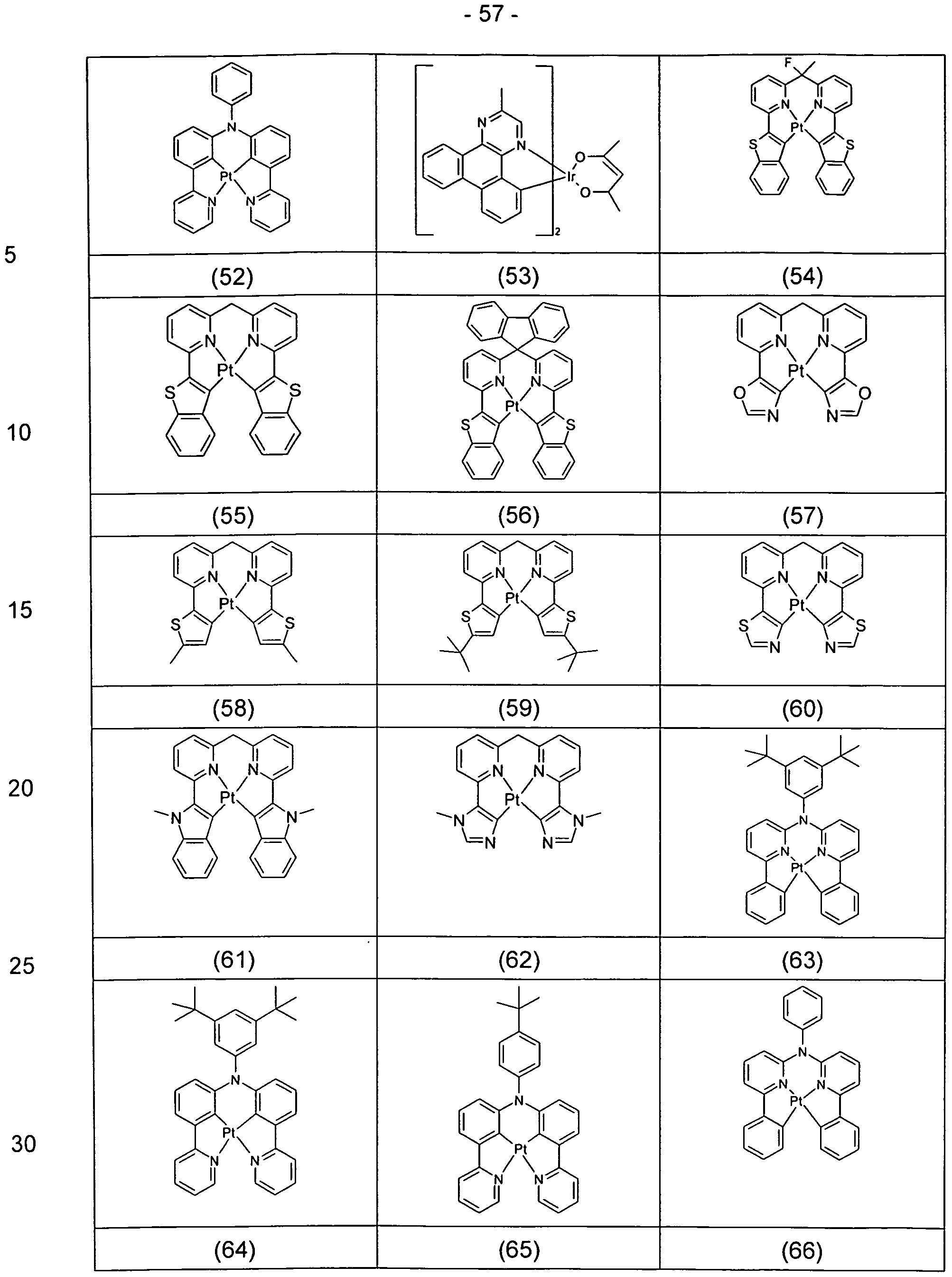
- Examples of suitable compounds according to formula (1a) are the compounds (1) to (62) depicted below.
- Suitable triazine derivatives which can be used as matrix material B are, in particular, 1,3,5-triazines which are substituted by at least one, preferably at least two, more preferably by three aromatic or heteroaromatic ring systems. Particular preference is thus given to compounds of the following formula (6) or (7)
- Formula (6) where R 1 has the abovementioned meaning and applies to the other symbols used: is identical or different at each occurrence, a monovalent aromatic or heteroaromatic ring system having 5 to 60 aromatic ring atoms, which may be substituted in each case with one or more radicals R 1 ; is a bivalent aromatic or heteroaromatic ring system having 5 to 60 aromatic ring atoms, which may be substituted by one or more R radicals.
- X is the same or different at each occurrence as a bivalent
- m is the same or different at each occurrence 0, 1, 2 or 3;
- o is the same or different 0, 1, 2, 3 or 4 at each occurrence.
- Particularly preferred groups Ar 2 are selected from the groups of the following formulas (8a) to (16a),
- X is preferably identical or different selected from C (R 1 ) 2 , N (R 1 ), O and S, particularly preferably C (R 1 ) 2 .
- Preferred Ar 3 groups in compounds of the formula (7) are selected from the groups of the following formulas (17) to (24),
- Particularly preferred groups Ar 3 are selected from the groups of the following formulas (17a) to (24a),
- X is preferably identical or different selected from C (R 1 ) 2 , N (R 1 ), O and S, particularly preferably C (R 1 ) 2 .
- the compound B is a pyrimidine derivative, it is preferably a pyrimidine derivative represented by the following formula (25), (26) or (27).
- At least one group Ar 2 is selected from the abovementioned groups of the formulas (8) to (16) or (8a) to (16a).
- the compound B is a hole-transporting compound.
- Suitable hole-transporting compounds B are preferably selected from carbazole derivatives, for. B. CBP ( ⁇ , ⁇ -biscarbazolylbiphenyl) or in WO 2005/039246, US 2005/0069729, JP 2004/288381, EP 1205527 or WO 2008/086851 disclosed carbazole derivatives, triarylamine derivatives, bridged carbazole derivatives, for. B. according to the unpublished application DE 102010005697.9, Indolocarbazolderivaten, z. B. according to WO 2007/063754 or WO 2008/056746, indenocarbazole derivatives, z. B. according to WO 2010/136109, Azacarbazolderivaten, z. B. according to EP 1617710, EP 1617711, EP 1731584, JP 2005/347160,
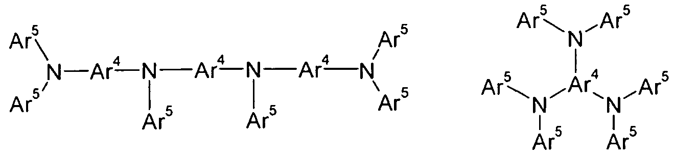
- Preferred aromatic amines and carbazoles are the compounds of the following formulas (28) to (33),
- Ar 4 is the same or different at each occurrence, a bivalent, trivalent or tetravalent aromatic or heteroaromatic ring system having 5 to 60 aromatic ring atoms, which may be substituted by one or more radicals R 1 ;
- Ar 4 in the compounds of the formulas (28), (29), (30) and (33) is a divalent group and in the compounds of the formula (31) a trivalent group and in the compounds of the formula (32) a tetra - Valente group, wherein Ar 4 as described above, in each case additionally by one or more radicals R 1 may be substituted. It is preferred if Ar 4 and Ar 5 are not condensed aryl or
- Heteroaryl groups containing more than 10 aromatic ring atoms are containing more than 10 aromatic ring atoms.
- Ar 4 and Ar 5 do not contain any fused aryl or heteroaryl groups.
- Formula (38) Formula (39) Formula (40) Formula (41) wherein these structures may also be substituted by one or more radicals R 1 and R 1 has the abovementioned meaning.
- two radicals R 1 which bind to the same C atom can form a ring with one another.
- the two radicals R 1 in formula (39), when they represent alkyl groups can span a cyclopentyl or a cyclohexyl group with the carbon atom to which they are attached.
- a spiro system for example a spirobifluorene, can be built up.
- Suitable hole-conducting matrix materials are also bridged carbazole derivatives, which preferably have a structure of the following formula (42),
- Formula (42) wherein X has the same meaning as described above and this structure may also be substituted by one or more substituents R 1 .
- At least one of the substituents R 1 is preferably a substituted or unsubstituted diaryl or heteroarylamino group, a substituted or unsubstituted triaryl or heteroarylamino group, a substituted or unsubstituted triazine group or a substituted or unsubstituted pyrimidine group.
- X is preferably C (R 1 ) 2 .
- Examples of suitable hole-conducting matrix materials B are the structures (1) to (55) listed in the following table.
- a further compound C is present in the emitting layer, this is preferably a compound as has already been mentioned above for the compounds B as being preferred, provided the abovementioned
- compound C may preferably be a material which has a large bandgap and is not or substantially not involved in charge transport or emission in the layer. These are preferably pure hydrocarbons, but also diazaborole derivatives. Examples of suitable compounds C are the compounds (1) to (19) depicted below.
- polymeric "binders” such as polystyrene, polycarbonate, polyvinyl butyral, polymethyl methacrylate as material C are preferred.
- conjugate-disrupted polymers can be used as materials C, as described in WO 2010/136111 and WO 2010/136110.
- Compounds that are particularly suitable as phosphorescent compound A are those which, with suitable excitation, emit light, preferably in the visible
- Preferred phosphorescence emitters used are compounds containing copper, molybdenum, tungsten, rhenium, ruthenium, osmium, rhodium, iridium, palladium, platinum, silver, gold or europium, in particular compounds containing iridium, platinum or copper.
- Particularly preferred organic electroluminescent devices contain at least one phosphorescent compound
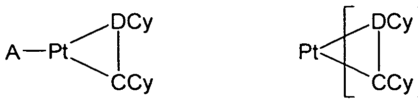
- DCy is the same or different at each occurrence, a cyclic one
- CCy is the same or different at each occurrence a cyclic
- A is the same or different at each occurrence as a mononionic, bidentate chelating ligand, preferably a diketonate ligand or a picolinate.
- Suitable and preferred groups DCy are, for example, pyridine, pyridazine, pyrimidine, pyrazine, triazine, quinoline, isoquinoline, imidazole, pyrazol or triazole, which in each case may be substituted by one or more radicals R. These groups coordinate to the metal via a nitrogen atom.
- Suitable and preferred groups CCy are, for example, phenyl, pyridine, thiophene, furan, pyrrole or naphthalene, which may each be substituted by one or more radicals R 1 . These groups bind to the metal via a carbon atom.
- R 1 a radical that may also be a bridge between the groups DCy and CCy.
- R 1 a bridge between two or three ligands CCy-DCy or between one or two ligands CCy-DCy and the ligand A, so that it is a polydentates or polypodal
- Examples of the emitters described above can be found in applications WO 2001/41512, WO 2002/02714, WO 2002/15645, EP 1191613, EP 1191612, EP 1191614, WO 2004/081017, WO 2005/033244, WO
- co-ligand p is 1, 2 or 3; q is 0, 1, 2, 3 or 4; It is also possible for several ligands L to be linked to one another or L to be linked to L 'via an arbitrary bridge V and thus for a tridentate, tetradentate, pentadentate or hexadentate ligand system to be spanned.
- Electron system contributes. Each nitrogen atom, which is bound in only one 6- ring, also contributes 1 ⁇ -electron to the entire electron system. Each nitrogen atom, which is simultaneously bound in a 5-ring and a 6-ring, carries 2 ⁇ electrons to the whole
- Each nitrogen atom which is only bound in a 5-membered ring, contributes 1 or 2 ⁇ electrons to the entire electron system. It depends on the binding of nitrogen in the 5-ring, whether this nitrogen atom contributes 1 or 2 ⁇ electrons to the entire electron system.
- the cycle in one cycle in formulas (2) and (3) represents a 6 ⁇ -electron system, as is customarily used for the preparation of aromatic or heteroaromatic structures in organic chemistry. The following structures explain again when the nitrogen 1 or 2 ⁇ -electrons (in the scheme only as
- Electrons contributes to the entire ⁇ electron system: ktrons via the lone pair of electrons
- a nitrogen atom with saturated valence in the context of this invention is understood as meaning a nitrogen atom which either formally enters into a single bond and a double bond or three single bonds within the aromatic backbone.
- the radical R 3 which is bonded to this nitrogen atom, represents a lone pair of electrons.
- a nitrogen atom with unsatisfied valence in the sense of this invention is understood to mean a nitrogen atom which undergoes formally only two single bonds within the aromatic backbone.
- the radical R 3 which is bonded to this nitrogen atom, represents a radical as defined above, and no free electron pair.
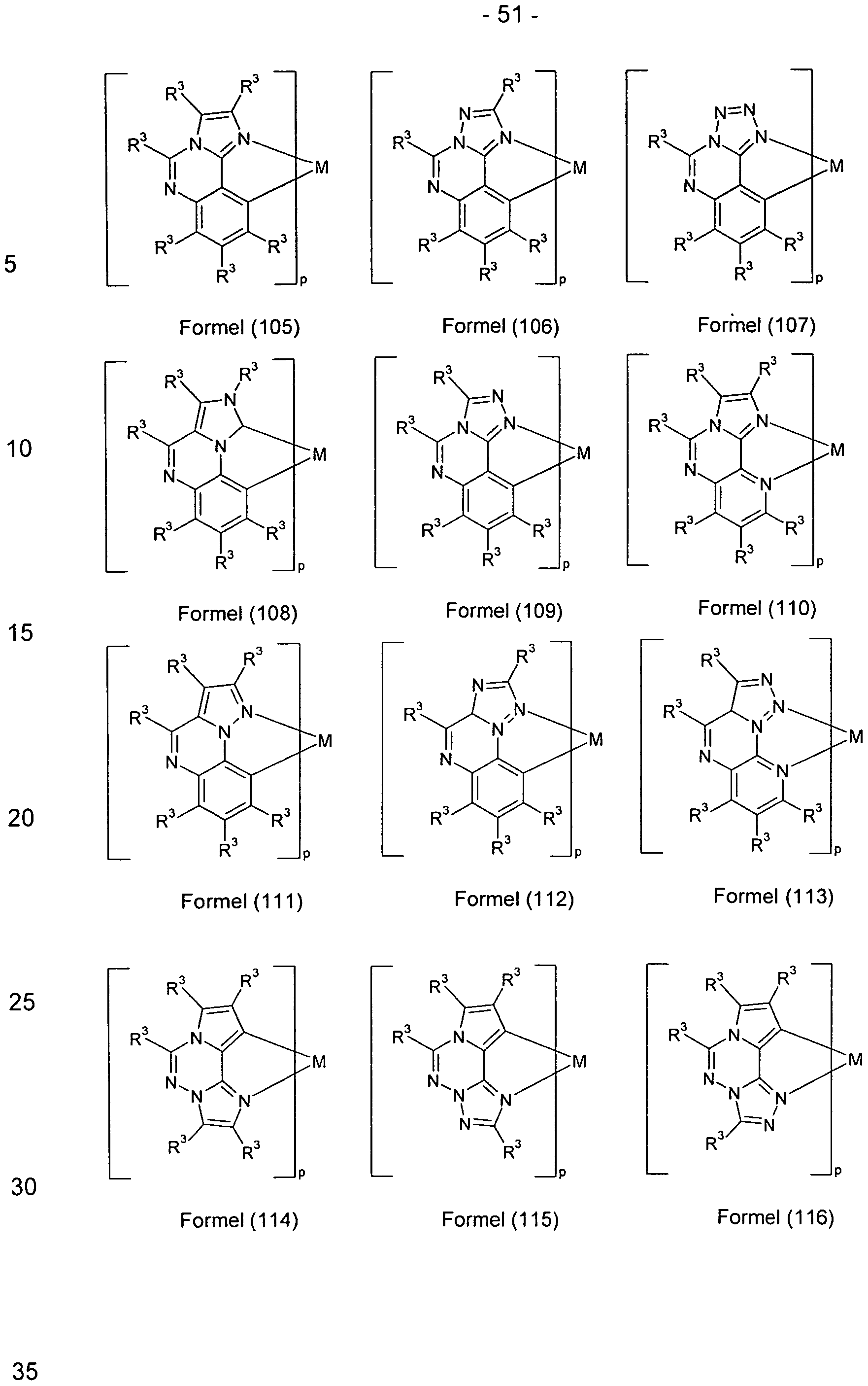
- a particularly preferred embodiment of the substructures according to the formulas (48) and (49) are the structures according to the following
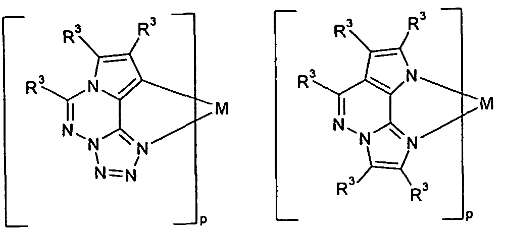
- Preferred embodiments in which the radicals R 3 form a ring system with one another are the structures of the following formulas (119) to (127),
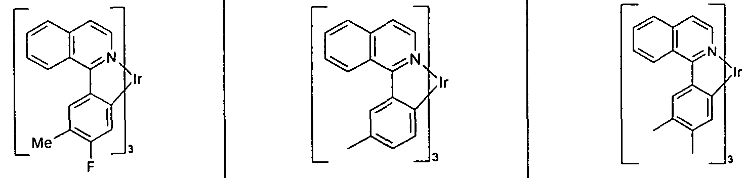
- Suitable phosphorescent compounds A are the structures (1) to (192) listed in the following table.
- the organic electroluminescent device may also contain further layers. These are for example selected from in each case one or more hole injection layers, Hole transport layers, hole blocking layers, electron transport layers, electron injection layers, electron blocking layers, exciton blocking layers, charge generation layers (charge generation layers) and / or organic or inorganic p / n junctions.
- interlayers may be present, which control, for example, the charge balance in the device.
- such interlayers may be useful as an intermediate layer between two emitting layers, in particular as an intermediate layer between a fluorescent and a phosphorescent layer.
- the layers, in particular the charge transport layers may also be doped. The doping of the layers may be improved
- Charge transport be beneficial. It should be noted, however, that not necessarily each of the above layers must be present and the choice of layers always depends on the compounds used. The use of such layers is known to the person skilled in the art, and he can use for this purpose, without inventive step, all materials known for such layers according to the prior art.
- a white-emitting organic electroluminescent device This is characterized by emitting light with CIE color coordinates in the range of 0.28 / 0.29 to 0.45 / 0.48.
- the general structure of such a white-emitting electroluminescent device is disclosed, for example, in WO 2005/011013.
- the organic electroluminescent device according to the invention leads to a color shift of the emission band to longer wavelengths compared to the emission of the pure emitter in solution and further to broader emission bands, this emission having a very high efficiency. It also depends on the matrix material used possible to obtain both the emission of the pure emitter and at the same time a longer-wave emission.
- a blue or blue-green phosphorescent emitter A in one layer into a compound with which none of the above conditions (1) or (2) are satisfied, and the same emitter A in another Layer, for example, adjacent to the first layer, in a compound B dope with either the above conditions (1) or the above conditions (2) are met.
- the first layer shows the blue or cyan emission of the emitter A
- the second layer shows a longer wavelength emission with broad emission band, resulting in white emission as a whole with good color coordinates and high efficiency.
- a blue or cyan phosphorescent emitter in one layer into a compound with which none of the above conditions (1) or (2) are satisfied, and another emitter A in another layer which, for example, adjoins the first layer to be doped into a compound B which fulfills either the abovementioned conditions (1) or the abovementioned conditions (2).
- the first layer shows the blue or cyan emission of emitter A
- the second layer shows longer wavelength emission, for example, yellow emission, with broad emission band, so that as a whole white emission with good color coordinates and high efficiency results.
- a blue or blue-green phosphorescent emitter A in one layer into a mixture of two or more different compounds, with at least one of the compounds satisfying none of the above-mentioned conditions (1) or (2) and with at least one further compound B either the abovementioned conditions (1) or the abovementioned conditions (2) are fulfilled.
- This layer shows both the blue or blue-green emission of the emitter A and a longer-wavelength emission with a broad emission band, so that Total white emission with good color coordinates results. Since this is an organic electroluminescent device with only one emission layer, such a device structure is also particularly suitable for the production of the electroluminescent device from solution.
- the cathode of the electroluminescent device according to the invention are low work function metals, metal alloys or multilayer structures of different metals, such as alkaline earth metals, alkali metals, main group metals or lanthanides (eg Ca, Ba, Mg, Al, In, Mg, Yb, Sm, Etc.).
- alkaline earth metals alkali metals
- main group metals or lanthanides eg Ca, Ba, Mg, Al, In, Mg, Yb, Sm, Etc.
- further metals which have a relatively high work function, such as, for example, B. Ag, which then usually combinations of metals, such as Mg / Ag, Ca / Ag or Ba / Ag, are used.
- metal alloys in particular alloys of an alkali metal or alkaline earth metal and silver, particularly preferably an alloy of Mg and Ag. It may also be preferred to introduce between a metallic cathode and the organic semiconductor a thin intermediate layer of a material with a high dielectric constant.
- alkali metal or alkaline earth metal fluorides but also the corresponding oxides or carbonates (eg LiF, L 12 O, CsF, CS 2 CO 3, BaF 2 , MgO, NaF, etc.).
- organic alkali metal complexes for example lithium quinolinate.
- the layer thickness of this layer is preferably between 0.5 and 5 nm.
- the anode has a work function greater than 4.5 eV. Vacuum up.
- metals with a high redox potential such as Ag, Pt or Au, are suitable for this purpose.
- metal / metal oxide electrode z. B. AI / Ni / NiO, AI / PtO x
- At least one of the Electrodes should be transparent or semi-transparent to allow the extraction of light.
- Preferred anode materials here are conductive mixed metal oxides. Particularly preferred are indium tin oxide (ITO) or indium zinc oxide (IZO). Preference is furthermore given to conductive, doped organic materials, in particular conductive doped polymers.
- the device is structured accordingly (depending on the application), contacted and finally hermetically sealed because the life of such devices drastically shortened in the presence of water and / or air.
- organic electroluminescent devices can be used in combination with the emitting layer according to the invention.
- the person skilled in the art knows which materials he can use for these layers or functions, and he can use these materials readily inventive step in the device structure of the organic electroluminescent device according to the invention.
- an organic electroluminescent device characterized in that one or more layers are coated with a sublimation process. The materials in vacuum sublimation systems become smaller at an initial pressure
- the initial pressure may be even lower, for example less than 0 ⁇ 7 mbar.
- an organic electroluminescent device characterized in that one or more layers are coated with the OVPD (Organic Vapor Phase Deposition) method or with the aid of a carrier gas sublimation.
- the materials are applied at a pressure between 10 "applied 5 mbar and 1 bar.
- OVJP organic vapor jet printing
- an organic electroluminescent device characterized in that one or more layers of solution, such. B. by spin coating, or with any printing process, such.
- any printing process such as screen printing, flexographic printing, offset printing, LITI (Light Induced Thermal Imaging, thermal transfer printing), ink-jet printing (inkjet printing) or Nozzle-Printing.
- screen printing flexographic printing, offset printing, LITI (Light Induced Thermal Imaging, thermal transfer printing), ink-jet printing (inkjet printing) or Nozzle-Printing
- soluble compounds are needed. High solubility can be achieved by suitable substitution of the compounds.
- solutions of individual materials can be applied, but also solutions containing several compounds, such as the phosphorescent
- the organic electroluminescent device may also be fabricated as a hybrid system by applying one or more layers of solution and depositing one or more further layers.
- Another object of the present invention is thus a
- Method for producing an organic electroluminescent device characterized in that at least one layer is applied by means of a sublimation method and / or that at least one layer is applied by the OVPD method and / or that at least one layer is applied from solution or by any printing method becomes.
- Another object of the present invention is therefore a formulation, preferably a solution, a suspension or a miniemulsion containing at least one phosphorescent compound A and at least one further compound B, wherein the above relationships apply to the compounds A and B.
- a formulation preferably a solution, a suspension or a miniemulsion containing at least one phosphorescent compound A and at least one further compound B, wherein the above relationships apply to the compounds A and B.
- organic electroluminescent devices are used, in particular for display applications or as a light source, for example for lighting applications or for medical or cosmetic applications.
- the organic electroluminescent devices according to the invention have the following surprising advantages over the prior art:
- the organic electroluminescent device according to the invention shows emission whose emission color is shifted from the emission of the emitter in solution to longer wavelengths.
- the color location of the emission and the width of the emission band of the organic electroluminescent device can be adjusted.
- the organic electroluminescent device according to the invention has a very high efficiency. This is surprising since, in general, emission from states due to intermolecular interactions has only a very low probability of transition and thus has only a low efficiency.
- Electroluminescent devices with the use of only a single emitter accessible by using different matrix materials in the same layer or in different layers. This represents a technical advantage in the production of the electroluminescent device, since less different
- the HOMO and LUMO layers of compounds A and B and the triplet level Ti of compounds B are determined by quantum chemical calculations.
- the program package "Gaussian03W” (Gaussian Inc.) is used
- Gasian Inc. For the calculation of organic substances without metals (in table 4 with method “org.")
- the geometry is determined by the method "Ground State / Hartree-jib / Default Spin / LanL2MB” (lot 0 / spin
- the energy calculation is analogous to the organic substances as described above with the difference that for the metal atom the
- HOMO (eV) ((HEh * 27.212) -0.9899) / 1 .1206 eV
- these values are to be regarded as the energetic position of the HOMO level or the LUMO level of the materials.
- HTM for the substance HTM from the calculation a HOMO of -0.17519 Hartrees and a LUMO of -0.04192 Hartrees, which gives a calibrated HOMO of -5.14 eV and a calibrated LUMO of
- Compound C is defined as the energy of the triplet state with the lowest energy, which results from the quantum chemical calculation.
- the triplet level of Ti of the phosphorescent compound A is obtained from the measurement of the Photolumineszenzmaximums the corresponding compound in toluene (10 "5 M solution) at room temperature.
- Table 4 shows the HOMO and LUMO values as well as the triplet levels Ti of the different materials.
- the triplet level in Table 4 is determined by measuring the photoluminescence maximum of the corresponding compound in toluene (10 ⁇ 5 molar solution) at room temperature.
- the triplet level is usually not possible by measuring the photoluminescence at room temperature, therefore the quantum chemical calculations are used for this, as described above.
- the OLEDs basically have the following layer structure: Substrate / optional hole injection layer (HIL) / hole transport layer (HTL) / electron blocking layer (EBL) / emission layer (EML) / optional hole blocking layer (HBL) / electron transport layer (ETL) / optional electron injection layer (EIL) and finally a cathode.
- HIL hole injection layer
- HTL hole transport layer
- EBL emission layer
- EML optional hole blocking layer
- HBL electron transport layer
- ETL optional electron transport layer
- EIL optional electron injection layer
- EIL electron injection layer
- cathode is formed by a 100 nm thick aluminum layer
- Emission layer always made of at least one matrix material (host material, host material) and an emitting dopant (dopant, emitter), the matrix material or the matrix materials
- Cover vaporization is mixed in a certain volume fraction.
- the charge transport layers may consist of a mixture of two or more materials. Table 1 shows by way of example components with electron transport layers which contain 2 materials (Examples 7 to 13). The exact structure of the OLEDs is shown in Table 1. The materials used to make the OLEDs are shown in Table 3.
- the OLEDs are characterized by default.
- the current efficiency (measured in cd / A), the external quantum efficiency (EQE, indication in%) and the voltage (measured in V) are determined from current-voltage-luminance characteristic curves (IUL characteristics).
- electroluminescence spectra (EL spectra) are measured. All data refer to the corresponding values at a luminance of 1000 cd / m 2 . Table 2 contains the data obtained for Examples 1 to 19.
- Figure 1 shows the normalized photoluminescence spectra of the emitters TEB-1, TEB-2, TEB-3 and TEG-1 used in a 10 ⁇ 5 molar solution in toluene. These spectra are used to determine the triplet level.
- Figure 2 shows the normalized electroluminescence spectra for Examples 1 and 2. In both examples, the concentration of emitters TEB-2 and TEB-3 in matrix M1 is 10%. From the fact that the effect of a broad band for both emitters occurs at approximately the same level, one can conclude that they are not aggregates of emitter molecules with one another, since TEB-3 is sterically more demanding due to its tert-butyl substituent, and has a correspondingly lower tendency to aggregate.
- Figure 3 shows the normalized electroluminescence spectra to the
- Figure 4 shows the normalized electroluminescence spectra for Examples 1, 5 and 6.
- concentration of the emitter TEB-2 is hereby kept constant at 10% but matrices with different LUMO levels are used.
- EQE the width of the emission and its efficiency
- the lowest efficiency shows the pure triplet emission of the emitter, which is a surprising result.
- FIG. 5 shows the normalized electroluminescence spectra for Examples 7 and 8.
- each 10% TEG-1 is used as an emitter.
- the emitter shows the typical green EL spectrum (example 7), in matrix M5 a broadened (example 8) or one with increased intensity in the longer-wave spectral range.
- This example shows that the effect is not limited to blue emitters and thus can be used to make devices with other mixed colors.
- Figure 6 shows the difference between ClEx and ClEy from the electro-luminescence spectra of TEG-1 in matrices M4 to M9 to ClEx and ClEy of TEG-1 in matrix M4 (Examples 7 to 12). This difference is in each case plotted against the LUMO values of the matrices.
- FIG. 7 shows the normalized electroluminescence spectrum of Example 17.
- the emitter TEB-1 in matrix M1 shows almost exclusively the broad band without actual triplet emission.
- Figure 8 shows the normalized electroluminescence spectra for Examples 18 and 19.
- the two matrices M1 and M3 are mixed together within one layer (Ex. 18) or two
- Example 13 to Example 16 show OLEDs with further emitters (TEB-4 to TEB-7) in different matrices, which also show a broadened emission or a broad band, as can be seen from the OLED data in Table 2.
- HIM HTM EBM2 M2 TEB-2 M1 AIQ LiF 20 nm 5 nm 15 nm (90%: 10%) 10 nm 20 nm 2 nm
- HIM HTM EBM1 M2 TEB-2 M1 AIQ LiF 20 nm 5 nm 15 nm (90%: 10%) 10 nm 20 nm 2 nm
- HIM HTM EBM1 M3 TEB-2 M1 AIQ LiF 20 nm 5 nm 15 nm (90%: 10%) 10 nm 20 nm 2 nm
- HIM HTM EBM1 M1 TEB-1 ETM2 LiQ 20 nm 5 nm 15 nm (90%: 10%) 30 nm 2 nm
- Table 2 OLED data for OLEDs from Table 1
Abstract
Description


Claims


Priority Applications (5)
| Application Number | Priority Date | Filing Date | Title |
|---|---|---|---|
| KR1020137005155A KR101877582B1 (en) | 2010-07-30 | 2011-06-24 | Organic electroluminescent device |
| JP2013522115A JP5968885B2 (en) | 2010-07-30 | 2011-06-24 | Organic electroluminescence device |
| CN201180037656.5A CN103053043B (en) | 2010-07-30 | 2011-06-24 | Organic electroluminescence device |
| DE112011102558.0T DE112011102558B4 (en) | 2010-07-30 | 2011-06-24 | Organic electroluminescent device |
| US13/812,341 US9236578B2 (en) | 2010-07-30 | 2011-06-24 | Organic electroluminescent device |
Applications Claiming Priority (2)
| Application Number | Priority Date | Filing Date | Title |
|---|---|---|---|
| EP10007953 | 2010-07-30 | ||
| EP10007953.2 | 2010-07-30 |
Publications (1)
| Publication Number | Publication Date |
|---|---|
| WO2012013271A1 true WO2012013271A1 (en) | 2012-02-02 |
Family
ID=44628264
Family Applications (1)
| Application Number | Title | Priority Date | Filing Date |
|---|---|---|---|
| PCT/EP2011/003134 WO2012013271A1 (en) | 2010-07-30 | 2011-06-24 | Organic electroluminescent device |
Country Status (6)
| Country | Link |
|---|---|
| US (1) | US9236578B2 (en) |
| JP (1) | JP5968885B2 (en) |
| KR (1) | KR101877582B1 (en) |
| CN (1) | CN103053043B (en) |
| DE (1) | DE112011102558B4 (en) |
| WO (1) | WO2012013271A1 (en) |
Cited By (19)
| Publication number | Priority date | Publication date | Assignee | Title |
|---|---|---|---|---|
| WO2012124622A1 (en) | 2011-03-14 | 2012-09-20 | 東レ株式会社 | Light-emitting element material and light-emitting element |
| WO2012153725A1 (en) | 2011-05-12 | 2012-11-15 | 東レ株式会社 | Light-emitting element material and light-emitting element |
| WO2013012296A1 (en) * | 2011-07-21 | 2013-01-24 | Rohm And Haas Electronic Materials Korea Ltd. | Novel organic electroluminescence compounds and organic electroluminescence device using the same |
| EP2581365A1 (en) * | 2011-10-10 | 2013-04-17 | Samsung Display Co., Ltd. | Heterocyclic compound, organic light-emitting diode comprising the heterocyclic compound, and flat panel display device comprising the organic light-emitting diode |
| EP2610937A1 (en) * | 2011-12-26 | 2013-07-03 | Samsung Display Co., Ltd. | Organic light emitting device with enhanced lifespan |
| JP2013243300A (en) * | 2012-05-22 | 2013-12-05 | Udc Ireland Ltd | Charge transport material, organic electroluminescent element, light-emitting device, display and illumination device |
| WO2014017484A1 (en) | 2012-07-25 | 2014-01-30 | 東レ株式会社 | Light emitting element material and light emitting element |
| CN103619986A (en) * | 2011-06-03 | 2014-03-05 | 默克专利有限公司 | Organic electroluminescence device |
| JP2014045101A (en) * | 2012-08-28 | 2014-03-13 | Konica Minolta Inc | Organic electroluminescent element, lighting device, and display device |
| WO2015004896A1 (en) * | 2013-07-11 | 2015-01-15 | 出光興産株式会社 | Compound and organic electroluminescent element using same |
| CN105074950A (en) * | 2013-04-08 | 2015-11-18 | 默克专利有限公司 | Organic electroluminescent device with thermally activated delayed fluorescence material |
| WO2016116530A1 (en) * | 2015-01-20 | 2016-07-28 | Cynora Gmbh | Compositions, in particular for use in optoelectronic components |
| WO2016124304A1 (en) * | 2015-02-03 | 2016-08-11 | Merck Patent Gmbh | Metal complexes |
| JP2017143289A (en) * | 2012-06-01 | 2017-08-17 | 株式会社半導体エネルギー研究所 | Light-emitting element |
| EP3244466A1 (en) * | 2016-05-10 | 2017-11-15 | Samsung Display Co., Ltd. | Organic light-emitting device |
| WO2018091435A1 (en) * | 2016-11-17 | 2018-05-24 | Merck Patent Gmbh | Materials for organic electroluminescent devices |
| US10658594B2 (en) | 2017-12-06 | 2020-05-19 | Idemitsu Kosan Co., Ltd. | Organic electroluminescence device and novel compound |
| US11856842B2 (en) | 2015-11-26 | 2023-12-26 | Samsung Display Co., Ltd. | Organic light-emitting device |
| US11910707B2 (en) | 2015-12-23 | 2024-02-20 | Samsung Display Co., Ltd. | Organic light-emitting device |
Families Citing this family (6)
| Publication number | Priority date | Publication date | Assignee | Title |
|---|---|---|---|---|
| EP2860782B1 (en) * | 2013-10-09 | 2019-04-17 | Novaled GmbH | Semiconducting material comprising a phosphine oxide matrix and metal salt |
| KR102273047B1 (en) * | 2014-06-30 | 2021-07-06 | 삼성디스플레이 주식회사 | Organic light-emitting device |
| KR102244081B1 (en) | 2014-08-13 | 2021-04-26 | 삼성디스플레이 주식회사 | Organic light emitting device |
| JP2016056169A (en) * | 2014-09-05 | 2016-04-21 | 株式会社半導体エネルギー研究所 | Organic compound, light-emitting element, light-emitting device, electronic device, and luminaire |
| KR102493553B1 (en) * | 2014-12-12 | 2023-01-30 | 메르크 파텐트 게엠베하 | Organic compounds with soluble groups |
| US10096658B2 (en) * | 2016-04-22 | 2018-10-09 | Semiconductor Energy Laboratory Co., Ltd. | Light-emitting element, display device, electronic device, and lighting device |
Citations (50)
| Publication number | Priority date | Publication date | Assignee | Title |
|---|---|---|---|---|
| US4539507A (en) | 1983-03-25 | 1985-09-03 | Eastman Kodak Company | Organic electroluminescent devices having improved power conversion efficiencies |
| US5151629A (en) | 1991-08-01 | 1992-09-29 | Eastman Kodak Company | Blue emitting internal junction organic electroluminescent device (I) |
| EP0676461A2 (en) | 1994-04-07 | 1995-10-11 | Hoechst Aktiengesellschaft | Spiro compounds and their application as electroluminescence materials |
| WO1998027136A1 (en) | 1996-12-16 | 1998-06-25 | Aventis Research & Technologies Gmbh & Co Kg | ARYL-SUBSTITUTED POLY(p-ARYLENE VINYLENES), METHOD FOR THE PRODUCTION AND USE THEREOF IN ELECTROLUMINESCENT COMPONENTS |
| WO2001041512A1 (en) | 1999-12-01 | 2001-06-07 | The Trustees Of Princeton University | Complexes of form l2mx as phosphorescent dopants for organic leds |
| WO2002002714A2 (en) | 2000-06-30 | 2002-01-10 | E.I. Du Pont De Nemours And Company | Electroluminescent iridium compounds with fluorinated phenylpyridines, phenylpyrimidines, and phenylquinolines and devices made with such compounds |
| WO2002015645A1 (en) | 2000-08-11 | 2002-02-21 | The Trustees Of Princeton University | Organometallic compounds and emission-shifting organic electrophosphorescence |
| EP1191614A2 (en) | 2000-09-26 | 2002-03-27 | Canon Kabushiki Kaisha | Luminescence device and metal coordination compound therefor |
| EP1191612A2 (en) | 2000-09-26 | 2002-03-27 | Canon Kabushiki Kaisha | Luminescence device, display apparatus and metal coordination compound |
| EP1191613A2 (en) | 2000-09-26 | 2002-03-27 | Canon Kabushiki Kaisha | Luminescence device, display apparatus and metal coordination compound |
| EP1205527A1 (en) | 2000-03-27 | 2002-05-15 | Idemitsu Kosan Co., Ltd. | Organic electroluminescence device |
| WO2002052661A1 (en) | 2000-12-22 | 2002-07-04 | Covion Organic Semiconductors Gmbh | Use of boron and aluminium compounds in electronic components |
| WO2003059015A1 (en) | 2001-12-28 | 2003-07-17 | The Trustees Of Princeton University | White light emitting oleds from combined monomer and aggregate emission |
| WO2004058911A2 (en) | 2002-12-23 | 2004-07-15 | Covion Organic Semiconductors Gmbh | Organic electroluminescent element |
| WO2004081017A1 (en) | 2003-03-11 | 2004-09-23 | Covion Organic Semiconductors Gmbh | Metal complexes |
| JP2004288381A (en) | 2003-03-19 | 2004-10-14 | Konica Minolta Holdings Inc | Organic electroluminescent element |
| WO2004093207A2 (en) | 2003-04-15 | 2004-10-28 | Covion Organic Semiconductors Gmbh | Mixtures of matrix materials and organic semiconductors capable of emission, use of the same and electronic components containing said mixtures |
| WO2005003253A2 (en) | 2003-07-07 | 2005-01-13 | Covion Organic Semiconductors Gmbh | Mixtures of organic emissive semiconductors and matrix materials, their use and electronic components comprising said materials |
| WO2005011013A1 (en) | 2003-07-21 | 2005-02-03 | Covion Organic Semiconductors Gmbh | Organic electroluminescent element |
| US20050069729A1 (en) | 2003-09-30 | 2005-03-31 | Konica Minolta Holdings, Inc. | Organic electroluminescent element, illuminator, display and compound |
| WO2005033244A1 (en) | 2003-09-29 | 2005-04-14 | Covion Organic Semiconductors Gmbh | Metal complexes |
| DE10343910A1 (en) * | 2003-09-19 | 2005-05-12 | Covion Organic Semiconductors | Organic electroluminescent device for semiconductors/organic LEDs has an anode, a cathode and a matrix layer with matrix material doped with a phosphorescent emitter |
| WO2005042550A1 (en) | 2003-10-30 | 2005-05-12 | Merck Patent Gmbh | Metal complexes with bipodal ligands |
| WO2005113563A1 (en) | 2004-05-19 | 2005-12-01 | Merck Patent Gmbh | Metal complexes |
| JP2005347160A (en) | 2004-06-04 | 2005-12-15 | Konica Minolta Holdings Inc | Organic electroluminescent element, lighting device, and display device |
| EP1617710A1 (en) | 2003-04-23 | 2006-01-18 | Konica Minolta Holdings, Inc. | Material for organic electroluminescent device, organic electroluminescent device, illuminating device and display |
| WO2006008069A1 (en) | 2004-07-16 | 2006-01-26 | Merck Patent Gmbh | Metal complexes |
| WO2006061182A1 (en) | 2004-12-09 | 2006-06-15 | Merck Patent Gmbh | Metal complexes and their use as the emitting constituent in electronic components, in particular in electroluminescent display devices |
| WO2006081973A1 (en) | 2005-02-03 | 2006-08-10 | Merck Patent Gmbh | Metal complexes |
| WO2006117052A1 (en) | 2005-05-03 | 2006-11-09 | Merck Patent Gmbh | Organic electroluminescent device and boric acid and borinic acid derivatives used therein |
| EP1731584A1 (en) | 2004-03-31 | 2006-12-13 | Konica Minolta Holdings, Inc. | Organic electroluminescent device material, organic electroluminescent device, display and illuminating device |
| WO2007063754A1 (en) | 2005-12-01 | 2007-06-07 | Nippon Steel Chemical Co., Ltd. | Compound for organic electroluminescent element and organic electroluminescent element |
| WO2007095118A2 (en) | 2006-02-10 | 2007-08-23 | Universal Display Corporation | METAL COMPLEXES OF CYCLOMETALLATED IMIDAZO[1,2-f]PHENANTHRIDINE AND DIIMIDAZO[1,2-A:1',2'-C]QUINAZOLINE LIGANDS AND ISOELECTRONIC AND BENZANNULATED ANALOGS THEREOF |
| WO2008056746A1 (en) | 2006-11-09 | 2008-05-15 | Nippon Steel Chemical Co., Ltd. | Compound for organic electroluminescent device and organic electroluminescent device |
| WO2008086851A1 (en) | 2007-01-18 | 2008-07-24 | Merck Patent Gmbh | Carbazole derivatives for organc electroluminescent devices |
| EP1998387A1 (en) * | 2006-03-17 | 2008-12-03 | Konica Minolta Holdings, Inc. | Organic electroluminescent device, display and illuminating device |
| WO2009062578A1 (en) | 2007-11-12 | 2009-05-22 | Merck Patent Gmbh | Organic electroluminescent devices comprising azomethine-metal complexes |
| WO2009118087A1 (en) | 2008-03-25 | 2009-10-01 | Merck Patent Gmbh | Metal complexes |
| WO2009146770A2 (en) | 2008-06-05 | 2009-12-10 | Merck Patent Gmbh | Electronic device comprising metal complexes |
| WO2009148015A1 (en) | 2008-06-05 | 2009-12-10 | 出光興産株式会社 | Halogen compound, polycyclic compound, and organic electroluminescence element comprising the polycyclic compound |
| WO2010006680A1 (en) | 2008-07-18 | 2010-01-21 | Merck Patent Gmbh | Materials for organic electroluminescence devices |
| WO2010015306A1 (en) | 2008-08-08 | 2010-02-11 | Merck Patent Gmbh, | Organic electroluminescence device |
| WO2010054730A1 (en) | 2008-11-11 | 2010-05-20 | Merck Patent Gmbh | Organic electroluminescent devices |
| WO2010054729A2 (en) | 2008-11-11 | 2010-05-20 | Merck Patent Gmbh | Materials for organic electroluminescence devices |
| US20100140605A1 (en) * | 2008-12-10 | 2010-06-10 | Fujifilm Corporation | Organic electroluminescence device and luminescence apparatus |
| WO2010086089A1 (en) | 2009-02-02 | 2010-08-05 | Merck Patent Gmbh | Metal complexes |
| WO2010136111A1 (en) | 2009-05-29 | 2010-12-02 | Merck Patent Gmbh | Composition, containing at least one emitter compound and at least one polymer with conjugation-interrupting units |
| WO2010136110A2 (en) | 2009-05-29 | 2010-12-02 | Merck Patent Gmbh | Polymers comprising substituted indenofluorene derivates as structural units, method for the production thereof, and use thereof |
| WO2010136109A1 (en) | 2009-05-29 | 2010-12-02 | Merck Patent Gmbh | Materials for organic electroluminescent devices |
| DE102010005697A1 (en) | 2010-01-25 | 2011-07-28 | Merck Patent GmbH, 64293 | Connections for electronic devices |
Family Cites Families (31)
| Publication number | Priority date | Publication date | Assignee | Title |
|---|---|---|---|---|
| US6310360B1 (en) * | 1999-07-21 | 2001-10-30 | The Trustees Of Princeton University | Intersystem crossing agents for efficient utilization of excitons in organic light emitting devices |
| JP3933591B2 (en) * | 2002-03-26 | 2007-06-20 | 淳二 城戸 | Organic electroluminescent device |
| AU2003240149A1 (en) * | 2002-05-31 | 2003-12-19 | Koninklijke Philips Electronics N.V. | Electroluminescent device |
| JP2005005149A (en) * | 2003-06-12 | 2005-01-06 | Tohoku Pioneer Corp | Organic el element and its manufacturing method |
| EP1668718B1 (en) | 2003-09-19 | 2009-03-25 | MERCK PATENT GmbH | Organic electroluminescent element |
| KR100773523B1 (en) * | 2003-11-06 | 2007-11-07 | 삼성에스디아이 주식회사 | Organometallic complexes and organic electroluminescence device using the same |
| JP2007512692A (en) | 2003-11-25 | 2007-05-17 | メルク パテント ゲーエムベーハー | Organic electroluminescence device |
| US7267892B2 (en) * | 2004-02-25 | 2007-09-11 | Eastman Kodak Company | Electroluminescent devices having pendant naphthylanthracene-based polymers |
| US20060008671A1 (en) * | 2004-07-07 | 2006-01-12 | Raymond Kwong | Electroluminescent efficiency |
| EP1784056B1 (en) * | 2004-07-23 | 2011-04-13 | Konica Minolta Holdings, Inc. | Organic electroluminescent device, display and illuminating device |
| US9040170B2 (en) * | 2004-09-20 | 2015-05-26 | Global Oled Technology Llc | Electroluminescent device with quinazoline complex emitter |
| KR100668305B1 (en) * | 2004-10-01 | 2007-01-12 | 삼성에스디아이 주식회사 | Cyclometalated transition metal complex and organic electroluminescence device using the same |
| JP4999322B2 (en) * | 2004-11-30 | 2012-08-15 | 株式会社半導体エネルギー研究所 | LIGHT EMITTING ELEMENT AND LIGHT EMITTING DEVICE HAVING THE LIGHT EMITTING ELEMENT |
| JP4496948B2 (en) | 2004-12-13 | 2010-07-07 | 株式会社豊田自動織機 | Organic EL device |
| US8415029B2 (en) * | 2004-12-29 | 2013-04-09 | Cambridge Display Technology Limited | Conjugated polymers prepared from rigid amines |
| US7683536B2 (en) * | 2005-03-31 | 2010-03-23 | The Trustees Of Princeton University | OLEDs utilizing direct injection to the triplet state |
| US8778507B2 (en) * | 2005-04-14 | 2014-07-15 | Konica Minolta Holdings, Inc. | Organic electroluminescent device, display and illuminating device |
| KR100611885B1 (en) * | 2005-04-21 | 2006-08-11 | 삼성에스디아이 주식회사 | Organic metal compounds which the compound for host and the compound for dopant were connected, organic electroluminescence display devices using the compounds and method for preparation of the devices |
| US20070252516A1 (en) | 2006-04-27 | 2007-11-01 | Eastman Kodak Company | Electroluminescent devices including organic EIL layer |
| US8273467B2 (en) * | 2006-02-28 | 2012-09-25 | Fujifilm Corporation | Organic electroluminescent device |
| US20070207345A1 (en) * | 2006-03-01 | 2007-09-06 | Eastman Kodak Company | Electroluminescent device including gallium complexes |
| EP1998388B1 (en) * | 2006-03-23 | 2017-04-19 | Konica Minolta Holdings, Inc. | Organic electroluminescent device, display and illuminating device |
| US7733009B2 (en) * | 2006-04-27 | 2010-06-08 | Global Oled Technology Llc | Electroluminescent device including an anthracene derivative |
| JP4690244B2 (en) | 2006-05-12 | 2011-06-01 | ケミプロ化成株式会社 | Fluorene compound having tetra-phenylsilane skeleton, light emitting layer host material, hole block material and organic EL device using the same |
| GB0617167D0 (en) | 2006-08-31 | 2006-10-11 | Cdt Oxford Ltd | Compounds for use in opto-electrical devices |
| US8372527B2 (en) * | 2007-07-11 | 2013-02-12 | Idemitsu Kosan Co., Ltd. | Material for organic electroluminescent element, and organic electroluminescent element |
| JP5130001B2 (en) * | 2007-07-27 | 2013-01-30 | 富士フイルム株式会社 | Organic electroluminescence device |
| JP5255794B2 (en) | 2007-07-27 | 2013-08-07 | ユー・ディー・シー アイルランド リミテッド | Organic electroluminescence device |
| JP4798128B2 (en) * | 2007-12-21 | 2011-10-19 | コニカミノルタホールディングス株式会社 | Organic electroluminescence element and display device |
| DE102008063470A1 (en) | 2008-12-17 | 2010-07-01 | Merck Patent Gmbh | Organic electroluminescent device |
| JP2017007559A (en) * | 2015-06-24 | 2017-01-12 | トヨタ自動車株式会社 | Hybrid automobile |
-
2011
- 2011-06-24 JP JP2013522115A patent/JP5968885B2/en active Active
- 2011-06-24 CN CN201180037656.5A patent/CN103053043B/en active Active
- 2011-06-24 US US13/812,341 patent/US9236578B2/en active Active
- 2011-06-24 WO PCT/EP2011/003134 patent/WO2012013271A1/en active Application Filing
- 2011-06-24 KR KR1020137005155A patent/KR101877582B1/en active IP Right Grant
- 2011-06-24 DE DE112011102558.0T patent/DE112011102558B4/en active Active
Patent Citations (52)
| Publication number | Priority date | Publication date | Assignee | Title |
|---|---|---|---|---|
| US4539507A (en) | 1983-03-25 | 1985-09-03 | Eastman Kodak Company | Organic electroluminescent devices having improved power conversion efficiencies |
| US5151629A (en) | 1991-08-01 | 1992-09-29 | Eastman Kodak Company | Blue emitting internal junction organic electroluminescent device (I) |
| EP0676461A2 (en) | 1994-04-07 | 1995-10-11 | Hoechst Aktiengesellschaft | Spiro compounds and their application as electroluminescence materials |
| WO1998027136A1 (en) | 1996-12-16 | 1998-06-25 | Aventis Research & Technologies Gmbh & Co Kg | ARYL-SUBSTITUTED POLY(p-ARYLENE VINYLENES), METHOD FOR THE PRODUCTION AND USE THEREOF IN ELECTROLUMINESCENT COMPONENTS |
| WO2001041512A1 (en) | 1999-12-01 | 2001-06-07 | The Trustees Of Princeton University | Complexes of form l2mx as phosphorescent dopants for organic leds |
| EP1205527A1 (en) | 2000-03-27 | 2002-05-15 | Idemitsu Kosan Co., Ltd. | Organic electroluminescence device |
| WO2002002714A2 (en) | 2000-06-30 | 2002-01-10 | E.I. Du Pont De Nemours And Company | Electroluminescent iridium compounds with fluorinated phenylpyridines, phenylpyrimidines, and phenylquinolines and devices made with such compounds |
| WO2002015645A1 (en) | 2000-08-11 | 2002-02-21 | The Trustees Of Princeton University | Organometallic compounds and emission-shifting organic electrophosphorescence |
| EP1191612A2 (en) | 2000-09-26 | 2002-03-27 | Canon Kabushiki Kaisha | Luminescence device, display apparatus and metal coordination compound |
| EP1191613A2 (en) | 2000-09-26 | 2002-03-27 | Canon Kabushiki Kaisha | Luminescence device, display apparatus and metal coordination compound |
| EP1191614A2 (en) | 2000-09-26 | 2002-03-27 | Canon Kabushiki Kaisha | Luminescence device and metal coordination compound therefor |
| WO2002052661A1 (en) | 2000-12-22 | 2002-07-04 | Covion Organic Semiconductors Gmbh | Use of boron and aluminium compounds in electronic components |
| WO2003059015A1 (en) | 2001-12-28 | 2003-07-17 | The Trustees Of Princeton University | White light emitting oleds from combined monomer and aggregate emission |
| WO2004058911A2 (en) | 2002-12-23 | 2004-07-15 | Covion Organic Semiconductors Gmbh | Organic electroluminescent element |
| WO2004081017A1 (en) | 2003-03-11 | 2004-09-23 | Covion Organic Semiconductors Gmbh | Metal complexes |
| JP2004288381A (en) | 2003-03-19 | 2004-10-14 | Konica Minolta Holdings Inc | Organic electroluminescent element |
| WO2004093207A2 (en) | 2003-04-15 | 2004-10-28 | Covion Organic Semiconductors Gmbh | Mixtures of matrix materials and organic semiconductors capable of emission, use of the same and electronic components containing said mixtures |
| EP1617711A1 (en) | 2003-04-23 | 2006-01-18 | Konica Minolta Holdings, Inc. | Organic electroluminescent device and display |
| EP1617710A1 (en) | 2003-04-23 | 2006-01-18 | Konica Minolta Holdings, Inc. | Material for organic electroluminescent device, organic electroluminescent device, illuminating device and display |
| WO2005003253A2 (en) | 2003-07-07 | 2005-01-13 | Covion Organic Semiconductors Gmbh | Mixtures of organic emissive semiconductors and matrix materials, their use and electronic components comprising said materials |
| WO2005011013A1 (en) | 2003-07-21 | 2005-02-03 | Covion Organic Semiconductors Gmbh | Organic electroluminescent element |
| DE10343910A1 (en) * | 2003-09-19 | 2005-05-12 | Covion Organic Semiconductors | Organic electroluminescent device for semiconductors/organic LEDs has an anode, a cathode and a matrix layer with matrix material doped with a phosphorescent emitter |
| WO2005033244A1 (en) | 2003-09-29 | 2005-04-14 | Covion Organic Semiconductors Gmbh | Metal complexes |
| WO2005039246A1 (en) | 2003-09-30 | 2005-04-28 | Konica Minolta Holdings, Inc. | Organic electroluminescent device, illuminating device, and display |
| US20050069729A1 (en) | 2003-09-30 | 2005-03-31 | Konica Minolta Holdings, Inc. | Organic electroluminescent element, illuminator, display and compound |
| WO2005042550A1 (en) | 2003-10-30 | 2005-05-12 | Merck Patent Gmbh | Metal complexes with bipodal ligands |
| EP1731584A1 (en) | 2004-03-31 | 2006-12-13 | Konica Minolta Holdings, Inc. | Organic electroluminescent device material, organic electroluminescent device, display and illuminating device |
| WO2005113563A1 (en) | 2004-05-19 | 2005-12-01 | Merck Patent Gmbh | Metal complexes |
| JP2005347160A (en) | 2004-06-04 | 2005-12-15 | Konica Minolta Holdings Inc | Organic electroluminescent element, lighting device, and display device |
| WO2006008069A1 (en) | 2004-07-16 | 2006-01-26 | Merck Patent Gmbh | Metal complexes |
| WO2006061182A1 (en) | 2004-12-09 | 2006-06-15 | Merck Patent Gmbh | Metal complexes and their use as the emitting constituent in electronic components, in particular in electroluminescent display devices |
| WO2006081973A1 (en) | 2005-02-03 | 2006-08-10 | Merck Patent Gmbh | Metal complexes |
| WO2006117052A1 (en) | 2005-05-03 | 2006-11-09 | Merck Patent Gmbh | Organic electroluminescent device and boric acid and borinic acid derivatives used therein |
| WO2007063754A1 (en) | 2005-12-01 | 2007-06-07 | Nippon Steel Chemical Co., Ltd. | Compound for organic electroluminescent element and organic electroluminescent element |
| WO2007095118A2 (en) | 2006-02-10 | 2007-08-23 | Universal Display Corporation | METAL COMPLEXES OF CYCLOMETALLATED IMIDAZO[1,2-f]PHENANTHRIDINE AND DIIMIDAZO[1,2-A:1',2'-C]QUINAZOLINE LIGANDS AND ISOELECTRONIC AND BENZANNULATED ANALOGS THEREOF |
| EP1998387A1 (en) * | 2006-03-17 | 2008-12-03 | Konica Minolta Holdings, Inc. | Organic electroluminescent device, display and illuminating device |
| WO2008056746A1 (en) | 2006-11-09 | 2008-05-15 | Nippon Steel Chemical Co., Ltd. | Compound for organic electroluminescent device and organic electroluminescent device |
| WO2008086851A1 (en) | 2007-01-18 | 2008-07-24 | Merck Patent Gmbh | Carbazole derivatives for organc electroluminescent devices |
| WO2009062578A1 (en) | 2007-11-12 | 2009-05-22 | Merck Patent Gmbh | Organic electroluminescent devices comprising azomethine-metal complexes |
| WO2009118087A1 (en) | 2008-03-25 | 2009-10-01 | Merck Patent Gmbh | Metal complexes |
| WO2009146770A2 (en) | 2008-06-05 | 2009-12-10 | Merck Patent Gmbh | Electronic device comprising metal complexes |
| WO2009148015A1 (en) | 2008-06-05 | 2009-12-10 | 出光興産株式会社 | Halogen compound, polycyclic compound, and organic electroluminescence element comprising the polycyclic compound |
| WO2010006680A1 (en) | 2008-07-18 | 2010-01-21 | Merck Patent Gmbh | Materials for organic electroluminescence devices |
| WO2010015306A1 (en) | 2008-08-08 | 2010-02-11 | Merck Patent Gmbh, | Organic electroluminescence device |
| WO2010054730A1 (en) | 2008-11-11 | 2010-05-20 | Merck Patent Gmbh | Organic electroluminescent devices |
| WO2010054729A2 (en) | 2008-11-11 | 2010-05-20 | Merck Patent Gmbh | Materials for organic electroluminescence devices |
| US20100140605A1 (en) * | 2008-12-10 | 2010-06-10 | Fujifilm Corporation | Organic electroluminescence device and luminescence apparatus |
| WO2010086089A1 (en) | 2009-02-02 | 2010-08-05 | Merck Patent Gmbh | Metal complexes |
| WO2010136111A1 (en) | 2009-05-29 | 2010-12-02 | Merck Patent Gmbh | Composition, containing at least one emitter compound and at least one polymer with conjugation-interrupting units |
| WO2010136110A2 (en) | 2009-05-29 | 2010-12-02 | Merck Patent Gmbh | Polymers comprising substituted indenofluorene derivates as structural units, method for the production thereof, and use thereof |
| WO2010136109A1 (en) | 2009-05-29 | 2010-12-02 | Merck Patent Gmbh | Materials for organic electroluminescent devices |
| DE102010005697A1 (en) | 2010-01-25 | 2011-07-28 | Merck Patent GmbH, 64293 | Connections for electronic devices |
Non-Patent Citations (1)
| Title |
|---|
| M. S. ARNOLD ET AL., APPL. PHYS. LETT., vol. 92, 2008, pages 053301 |
Cited By (30)
| Publication number | Priority date | Publication date | Assignee | Title |
|---|---|---|---|---|
| WO2012124622A1 (en) | 2011-03-14 | 2012-09-20 | 東レ株式会社 | Light-emitting element material and light-emitting element |
| WO2012153725A1 (en) | 2011-05-12 | 2012-11-15 | 東レ株式会社 | Light-emitting element material and light-emitting element |
| CN103619986A (en) * | 2011-06-03 | 2014-03-05 | 默克专利有限公司 | Organic electroluminescence device |
| US9118022B2 (en) * | 2011-06-03 | 2015-08-25 | Merck Patent Gmbh | Organic electroluminescent device |
| US20140088305A1 (en) * | 2011-06-03 | 2014-03-27 | Merck Patent Gmbh | Organic electroluminescent device |
| WO2013012296A1 (en) * | 2011-07-21 | 2013-01-24 | Rohm And Haas Electronic Materials Korea Ltd. | Novel organic electroluminescence compounds and organic electroluminescence device using the same |
| EP2581365A1 (en) * | 2011-10-10 | 2013-04-17 | Samsung Display Co., Ltd. | Heterocyclic compound, organic light-emitting diode comprising the heterocyclic compound, and flat panel display device comprising the organic light-emitting diode |
| US9309197B2 (en) | 2011-10-10 | 2016-04-12 | Samsung Display Co., Ltd. | Heterocyclic compound, organic light-emitting diode comprising the heterocyclic compound, and flat panel display device comprising the organic light-emitting diode |
| US9515280B2 (en) | 2011-12-26 | 2016-12-06 | Samsung Display Co., Ltd. | Organic light emitting device with enhanced lifespan |
| EP2610937A1 (en) * | 2011-12-26 | 2013-07-03 | Samsung Display Co., Ltd. | Organic light emitting device with enhanced lifespan |
| JP2013243300A (en) * | 2012-05-22 | 2013-12-05 | Udc Ireland Ltd | Charge transport material, organic electroluminescent element, light-emitting device, display and illumination device |
| JP2017143289A (en) * | 2012-06-01 | 2017-08-17 | 株式会社半導体エネルギー研究所 | Light-emitting element |
| WO2014017484A1 (en) | 2012-07-25 | 2014-01-30 | 東レ株式会社 | Light emitting element material and light emitting element |
| JP2014045101A (en) * | 2012-08-28 | 2014-03-13 | Konica Minolta Inc | Organic electroluminescent element, lighting device, and display device |
| CN105074950A (en) * | 2013-04-08 | 2015-11-18 | 默克专利有限公司 | Organic electroluminescent device with thermally activated delayed fluorescence material |
| US10069079B2 (en) | 2013-04-08 | 2018-09-04 | Merck Patent Gmbh | Organic electroluminescent device with thermally activated delayed fluorescence material |
| US10505123B2 (en) | 2013-07-11 | 2019-12-10 | Idemitsu Kosan Co., Ltd. | Compound and organic electroluminescent device using same |
| WO2015004896A1 (en) * | 2013-07-11 | 2015-01-15 | 出光興産株式会社 | Compound and organic electroluminescent element using same |
| WO2016116530A1 (en) * | 2015-01-20 | 2016-07-28 | Cynora Gmbh | Compositions, in particular for use in optoelectronic components |
| WO2016124304A1 (en) * | 2015-02-03 | 2016-08-11 | Merck Patent Gmbh | Metal complexes |
| US11024815B2 (en) | 2015-02-03 | 2021-06-01 | Merck Patent Gmbh | Metal complexes |
| US11856842B2 (en) | 2015-11-26 | 2023-12-26 | Samsung Display Co., Ltd. | Organic light-emitting device |
| US11910707B2 (en) | 2015-12-23 | 2024-02-20 | Samsung Display Co., Ltd. | Organic light-emitting device |
| EP3244466A1 (en) * | 2016-05-10 | 2017-11-15 | Samsung Display Co., Ltd. | Organic light-emitting device |
| US11696499B2 (en) | 2016-05-10 | 2023-07-04 | Samsung Display Co., Ltd. | Organic light-emitting device |
| WO2018091435A1 (en) * | 2016-11-17 | 2018-05-24 | Merck Patent Gmbh | Materials for organic electroluminescent devices |
| KR20190085032A (en) * | 2016-11-17 | 2019-07-17 | 메르크 파텐트 게엠베하 | Material for organic electroluminescence device |
| KR102580980B1 (en) | 2016-11-17 | 2023-09-20 | 메르크 파텐트 게엠베하 | Materials for organic electroluminescent devices |
| US10658594B2 (en) | 2017-12-06 | 2020-05-19 | Idemitsu Kosan Co., Ltd. | Organic electroluminescence device and novel compound |
| US10672989B2 (en) | 2017-12-06 | 2020-06-02 | Idemitsu Kosan Co., Ltd. | Organic electroluminescence device and novel compound |
Also Published As
| Publication number | Publication date |
|---|---|
| DE112011102558B4 (en) | 2022-01-05 |
| US20130168663A1 (en) | 2013-07-04 |
| JP2013539207A (en) | 2013-10-17 |
| DE112011102558A5 (en) | 2013-05-08 |
| US9236578B2 (en) | 2016-01-12 |
| JP5968885B2 (en) | 2016-08-10 |
| CN103053043B (en) | 2016-03-16 |
| KR101877582B1 (en) | 2018-07-12 |
| KR20130097740A (en) | 2013-09-03 |
| CN103053043A (en) | 2013-04-17 |
Similar Documents
| Publication | Publication Date | Title |
|---|---|---|
| DE112011102558B4 (en) | Organic electroluminescent device | |
| EP2695213B1 (en) | Organic electroluminescent device | |
| DE112010001236B4 (en) | ORGANIC ELECTROLUMINESCENCE DEVICE | |
| EP2303815B1 (en) | Organic electroluminescent device | |
| DE102009012346B4 (en) | Organic electroluminescent device and method for producing the same | |
| EP2984151B1 (en) | Organic electroluminescent device | |
| EP2984692B1 (en) | Organic electroluminescence device with thermally activated delayed fluorescence (tadf) material | |
| DE112011101604B4 (en) | Organic electroluminescent device | |
| DE102008063490B4 (en) | Organic electroluminescent device and method for adjusting the color locus of a white-emitting electroluminescent device | |
| DE102010010481A1 (en) | Organic electroluminescent device | |
| WO2014166586A1 (en) | Organic electroluminescent device | |
| EP2764558B1 (en) | Organic electroluminescent device | |
| WO2010069442A1 (en) | Organic electroluminescence device | |
| WO2013135352A1 (en) | Electronic devices | |
| EP2748878A1 (en) | Organic electroluminescence device | |
| WO2014194971A1 (en) | Organic electroluminescent device | |
| DE102010048497A1 (en) | Formulations for organic electroluminescent devices | |
| WO2010115498A1 (en) | Organic electroluminescence device |
Legal Events
| Date | Code | Title | Description |
|---|---|---|---|
| WWE | Wipo information: entry into national phase |
Ref document number: 201180037656.5 Country of ref document: CN |
|
| 121 | Ep: the epo has been informed by wipo that ep was designated in this application |
Ref document number: 11730568 Country of ref document: EP Kind code of ref document: A1 |
|
| ENP | Entry into the national phase |
Ref document number: 2013522115 Country of ref document: JP Kind code of ref document: A |
|
| WWE | Wipo information: entry into national phase |
Ref document number: 112011102558 Country of ref document: DE Ref document number: 1120111025580 Country of ref document: DE |
|
| ENP | Entry into the national phase |
Ref document number: 20137005155 Country of ref document: KR Kind code of ref document: A |
|
| WWE | Wipo information: entry into national phase |
Ref document number: 13812341 Country of ref document: US |
|
| REG | Reference to national code |
Ref country code: DE Ref legal event code: R225 Ref document number: 112011102558 Country of ref document: DE Effective date: 20130508 |
|
| 122 | Ep: pct application non-entry in european phase |
Ref document number: 11730568 Country of ref document: EP Kind code of ref document: A1 |