WO2012004922A1 - 液晶表示システム及び液晶表示システムの制御方法 - Google Patents
液晶表示システム及び液晶表示システムの制御方法 Download PDFInfo
- Publication number
- WO2012004922A1 WO2012004922A1 PCT/JP2011/002709 JP2011002709W WO2012004922A1 WO 2012004922 A1 WO2012004922 A1 WO 2012004922A1 JP 2011002709 W JP2011002709 W JP 2011002709W WO 2012004922 A1 WO2012004922 A1 WO 2012004922A1
- Authority
- WO
- WIPO (PCT)
- Prior art keywords
- liquid crystal
- light
- crystal display
- display panel
- state
- Prior art date
- Legal status (The legal status is an assumption and is not a legal conclusion. Google has not performed a legal analysis and makes no representation as to the accuracy of the status listed.)
- Ceased
Links
Images











Classifications
-
- G—PHYSICS
- G09—EDUCATION; CRYPTOGRAPHY; DISPLAY; ADVERTISING; SEALS
- G09G—ARRANGEMENTS OR CIRCUITS FOR CONTROL OF INDICATING DEVICES USING STATIC MEANS TO PRESENT VARIABLE INFORMATION
- G09G3/00—Control arrangements or circuits, of interest only in connection with visual indicators other than cathode-ray tubes
- G09G3/20—Control arrangements or circuits, of interest only in connection with visual indicators other than cathode-ray tubes for presentation of an assembly of a number of characters, e.g. a page, by composing the assembly by combination of individual elements arranged in a matrix no fixed position being assigned to or needed to be assigned to the individual characters or partial characters
- G09G3/34—Control arrangements or circuits, of interest only in connection with visual indicators other than cathode-ray tubes for presentation of an assembly of a number of characters, e.g. a page, by composing the assembly by combination of individual elements arranged in a matrix no fixed position being assigned to or needed to be assigned to the individual characters or partial characters by control of light from an independent source
- G09G3/36—Control arrangements or circuits, of interest only in connection with visual indicators other than cathode-ray tubes for presentation of an assembly of a number of characters, e.g. a page, by composing the assembly by combination of individual elements arranged in a matrix no fixed position being assigned to or needed to be assigned to the individual characters or partial characters by control of light from an independent source using liquid crystals
- G09G3/3611—Control of matrices with row and column drivers
- G09G3/3648—Control of matrices with row and column drivers using an active matrix
- G09G3/3651—Control of matrices with row and column drivers using an active matrix using multistable liquid crystals, e.g. ferroelectric liquid crystals
-
- G—PHYSICS
- G09—EDUCATION; CRYPTOGRAPHY; DISPLAY; ADVERTISING; SEALS
- G09G—ARRANGEMENTS OR CIRCUITS FOR CONTROL OF INDICATING DEVICES USING STATIC MEANS TO PRESENT VARIABLE INFORMATION
- G09G3/00—Control arrangements or circuits, of interest only in connection with visual indicators other than cathode-ray tubes
- G09G3/20—Control arrangements or circuits, of interest only in connection with visual indicators other than cathode-ray tubes for presentation of an assembly of a number of characters, e.g. a page, by composing the assembly by combination of individual elements arranged in a matrix no fixed position being assigned to or needed to be assigned to the individual characters or partial characters
- G09G3/34—Control arrangements or circuits, of interest only in connection with visual indicators other than cathode-ray tubes for presentation of an assembly of a number of characters, e.g. a page, by composing the assembly by combination of individual elements arranged in a matrix no fixed position being assigned to or needed to be assigned to the individual characters or partial characters by control of light from an independent source
- G09G3/3406—Control of illumination source
-
- G—PHYSICS
- G09—EDUCATION; CRYPTOGRAPHY; DISPLAY; ADVERTISING; SEALS
- G09G—ARRANGEMENTS OR CIRCUITS FOR CONTROL OF INDICATING DEVICES USING STATIC MEANS TO PRESENT VARIABLE INFORMATION
- G09G3/00—Control arrangements or circuits, of interest only in connection with visual indicators other than cathode-ray tubes
- G09G3/20—Control arrangements or circuits, of interest only in connection with visual indicators other than cathode-ray tubes for presentation of an assembly of a number of characters, e.g. a page, by composing the assembly by combination of individual elements arranged in a matrix no fixed position being assigned to or needed to be assigned to the individual characters or partial characters
- G09G3/34—Control arrangements or circuits, of interest only in connection with visual indicators other than cathode-ray tubes for presentation of an assembly of a number of characters, e.g. a page, by composing the assembly by combination of individual elements arranged in a matrix no fixed position being assigned to or needed to be assigned to the individual characters or partial characters by control of light from an independent source
- G09G3/36—Control arrangements or circuits, of interest only in connection with visual indicators other than cathode-ray tubes for presentation of an assembly of a number of characters, e.g. a page, by composing the assembly by combination of individual elements arranged in a matrix no fixed position being assigned to or needed to be assigned to the individual characters or partial characters by control of light from an independent source using liquid crystals
- G09G3/3611—Control of matrices with row and column drivers
- G09G3/3648—Control of matrices with row and column drivers using an active matrix
-
- G—PHYSICS
- G02—OPTICS
- G02F—OPTICAL DEVICES OR ARRANGEMENTS FOR THE CONTROL OF LIGHT BY MODIFICATION OF THE OPTICAL PROPERTIES OF THE MEDIA OF THE ELEMENTS INVOLVED THEREIN; NON-LINEAR OPTICS; FREQUENCY-CHANGING OF LIGHT; OPTICAL LOGIC ELEMENTS; OPTICAL ANALOGUE/DIGITAL CONVERTERS
- G02F1/00—Devices or arrangements for the control of the intensity, colour, phase, polarisation or direction of light arriving from an independent light source, e.g. switching, gating or modulating; Non-linear optics
- G02F1/01—Devices or arrangements for the control of the intensity, colour, phase, polarisation or direction of light arriving from an independent light source, e.g. switching, gating or modulating; Non-linear optics for the control of the intensity, phase, polarisation or colour
- G02F1/13—Devices or arrangements for the control of the intensity, colour, phase, polarisation or direction of light arriving from an independent light source, e.g. switching, gating or modulating; Non-linear optics for the control of the intensity, phase, polarisation or colour based on liquid crystals, e.g. single liquid crystal display cells
- G02F1/133—Constructional arrangements; Operation of liquid crystal cells; Circuit arrangements
- G02F1/1333—Constructional arrangements; Manufacturing methods
- G02F1/1334—Constructional arrangements; Manufacturing methods based on polymer dispersed liquid crystals, e.g. microencapsulated liquid crystals
-
- G—PHYSICS
- G02—OPTICS
- G02F—OPTICAL DEVICES OR ARRANGEMENTS FOR THE CONTROL OF LIGHT BY MODIFICATION OF THE OPTICAL PROPERTIES OF THE MEDIA OF THE ELEMENTS INVOLVED THEREIN; NON-LINEAR OPTICS; FREQUENCY-CHANGING OF LIGHT; OPTICAL LOGIC ELEMENTS; OPTICAL ANALOGUE/DIGITAL CONVERTERS
- G02F1/00—Devices or arrangements for the control of the intensity, colour, phase, polarisation or direction of light arriving from an independent light source, e.g. switching, gating or modulating; Non-linear optics
- G02F1/01—Devices or arrangements for the control of the intensity, colour, phase, polarisation or direction of light arriving from an independent light source, e.g. switching, gating or modulating; Non-linear optics for the control of the intensity, phase, polarisation or colour
- G02F1/13—Devices or arrangements for the control of the intensity, colour, phase, polarisation or direction of light arriving from an independent light source, e.g. switching, gating or modulating; Non-linear optics for the control of the intensity, phase, polarisation or colour based on liquid crystals, e.g. single liquid crystal display cells
- G02F1/133—Constructional arrangements; Operation of liquid crystal cells; Circuit arrangements
- G02F1/1333—Constructional arrangements; Manufacturing methods
- G02F1/1347—Arrangement of liquid crystal layers or cells in which the final condition of one light beam is achieved by the addition of the effects of two or more layers or cells
- G02F1/13476—Arrangement of liquid crystal layers or cells in which the final condition of one light beam is achieved by the addition of the effects of two or more layers or cells in which at least one liquid crystal cell or layer assumes a scattering state
-
- G—PHYSICS
- G09—EDUCATION; CRYPTOGRAPHY; DISPLAY; ADVERTISING; SEALS
- G09G—ARRANGEMENTS OR CIRCUITS FOR CONTROL OF INDICATING DEVICES USING STATIC MEANS TO PRESENT VARIABLE INFORMATION
- G09G2300/00—Aspects of the constitution of display devices
- G09G2300/02—Composition of display devices
- G09G2300/023—Display panel composed of stacked panels
-
- G—PHYSICS
- G09—EDUCATION; CRYPTOGRAPHY; DISPLAY; ADVERTISING; SEALS
- G09G—ARRANGEMENTS OR CIRCUITS FOR CONTROL OF INDICATING DEVICES USING STATIC MEANS TO PRESENT VARIABLE INFORMATION
- G09G2320/00—Control of display operating conditions
- G09G2320/06—Adjustment of display parameters
- G09G2320/0626—Adjustment of display parameters for control of overall brightness
-
- G—PHYSICS
- G09—EDUCATION; CRYPTOGRAPHY; DISPLAY; ADVERTISING; SEALS
- G09G—ARRANGEMENTS OR CIRCUITS FOR CONTROL OF INDICATING DEVICES USING STATIC MEANS TO PRESENT VARIABLE INFORMATION
- G09G2320/00—Control of display operating conditions
- G09G2320/06—Adjustment of display parameters
- G09G2320/066—Adjustment of display parameters for control of contrast
-
- G—PHYSICS
- G09—EDUCATION; CRYPTOGRAPHY; DISPLAY; ADVERTISING; SEALS
- G09G—ARRANGEMENTS OR CIRCUITS FOR CONTROL OF INDICATING DEVICES USING STATIC MEANS TO PRESENT VARIABLE INFORMATION
- G09G2360/00—Aspects of the architecture of display systems
- G09G2360/14—Detecting light within display terminals, e.g. using a single or a plurality of photosensors
- G09G2360/144—Detecting light within display terminals, e.g. using a single or a plurality of photosensors the light being ambient light
Definitions
- the present invention relates to a liquid crystal display system used for digital signage and the like, and a control method for the liquid crystal display system.
- Patent Documents 1 and 2 which advertises by playing high-quality video such as high-definition image quality on the display of the image display panel outdoors or in stores. System exists.
- Digital signage can distribute advertisements and the like by distributing and displaying moving images and still images on an image display panel using a network or the like. Since this digital signage display has the advantages of being thin, light and low power consumption, for example, a liquid crystal display panel is often used as an image display panel.
- Patent Document 3 discloses a liquid crystal display device having a display region in which a plurality of subpixels each having a region and a light transmission region are formed.
- This liquid crystal display device is configured such that the light reflection region and the light transmission region of each of the plurality of sub-pixels are driven independently of each other.
- the light reflection region is temporarily DC-driven to display a specific image.
- the specific image is continuously displayed on the display even when the power is off.
- the present invention has been made in view of such problems, and even when the image display panel is turned off and power consumption is reduced, information display that can be sufficiently used as a transmission medium for advertisements and advertisements.
- An object of the present invention is to provide a liquid crystal display system capable of realizing the above.
- a liquid crystal display system is formed by overlapping an image display panel for forming an image and a light scattering liquid crystal display panel having a light scattering liquid crystal layer between electrodes.
- a light-scattering pixel is formed to scatter incident light, thereby performing bright color display at a predetermined location on the light-scattering liquid crystal display panel and light.
- pixels in the transmissive state and performing dark color display on other parts of the light-scattering liquid crystal display panel By forming pixels in the transmissive state and performing dark color display on other parts of the light-scattering liquid crystal display panel, a light-dark image comprising a combination of these light-color display and dark-color display is displayed on the light-scattering liquid crystal display panel.
- the liquid crystal display system includes a first transparent substrate having a first electrode and disposed on the front side, and a second having a second electrode and disposed on the back side.
- a transparent substrate and a light-scattering liquid crystal layer disposed between the first transparent substrate and the second transparent substrate so that the first electrode and the second electrode face each other;
- a light-scattering liquid crystal display panel configured as described above, an image display panel that is disposed on the back side of the light-scattering liquid crystal display panel and forms an image, and a liquid crystal control unit that controls the alignment state of the liquid crystal In the first state in which the image display panel forms an image, the liquid crystal controller forms an electric field between the first electrode and the second electrode in the light-scattering liquid crystal display panel, thereby scattering light.
- the liquid crystal layer is in a light transmitting state, and the image formed by the image display panel is converted into a light scattering liquid.
- the second display is performed at a predetermined position on the light-scattering liquid crystal display panel.
- An electric field is formed between the first electrode and the second electrode to make the light-scattering liquid crystal layer in a light-transmitting state for dark color display, and at other locations on the light-scattering liquid crystal display panel, between the electrodes.
- the light-scattering liquid crystal layer is in a light-scattering state by forming an electric field to scatter external light to display bright colors, and a light-dark image composed of a combination of the light-color display and the dark-color display is displayed on the light-scattering liquid crystal display. It is displayed on a panel.
- the bright color display is a color display recognized based on scattered light, for example, white display.
- the dark color display is a color display recognized based on the fact that external light does not pass through the aligned light-scattering liquid crystal layer and is reflected, for example, black display or gray display.
- the light-scattering liquid crystal layer means that when no voltage is applied, the alignment state of the liquid crystal molecules is random, and the incident light is scattered and appears white (the liquid crystal shutter is closed).
- the liquid crystal layer has a behavior in which the liquid crystal molecules are aligned in parallel to the electric field and transmit light (the liquid crystal shutter is opened).
- pixels in the light scattering state are formed on the light scattering liquid crystal display panel to perform bright color display at a predetermined location, and in the light transmission state.
- a light / dark image composed of a combination of light color display and dark color display can be formed on a light-scattering liquid crystal display panel, thus saving power consumption
- advertising and advertising functions can be sufficiently performed.
- the image display panel may include a third transparent substrate on which a third electrode is disposed, a fourth transparent substrate on which a fourth electrode is disposed, and the third electrode and the fourth electrode so as to face each other.
- a liquid crystal display panel having a liquid crystal layer disposed between a third transparent substrate and the fourth transparent substrate and sealed between the third transparent substrate, the third transparent substrate of the liquid crystal display panel, and the light It is also possible to dispose the second liquid crystal display panel so as to face the second transparent substrate. According to this configuration, the image display panel can be configured with low power consumption and a thin shape.
- the liquid crystal control unit preferably places the liquid crystal layer of the liquid crystal display panel in a light non-transmissive state.
- the liquid crystal layer of the liquid crystal display panel in the second state, is in a light non-transmissive state, so that light from the back side of the liquid crystal display panel does not pass through the liquid crystal display panel, and thus the light scattering liquid crystal A dark color display formed at a predetermined position on the display panel can be displayed clearly.
- a state it is preferable to turn on the backlight, while in the case of the second state, it is preferable to turn off the backlight or turn it on in a low power consumption state.
- lighting the backlight in a low power consumption state means that the light emission portion of the backlight is lit dimly to suppress power consumption.
- the image in the first state, the image can be brightly displayed by backlight illumination.
- the backlight in the second state, the backlight is turned off or in a low power consumption state. Power saving can be achieved.
- the backlight control includes a backlight having a plurality of light emitting units that irradiate illumination light on the back side of the liquid crystal display panel, and a backlight control unit that controls lighting and extinguishing states of the backlight.
- the unit turns on the backlight in the first state, while turning on a part of the light emitting unit and turns off the other part in the second state. Even in this configuration, in the second state, only a part of the backlight is lit, so that power saving can be achieved.
- the liquid crystal control unit includes a backlight having a plurality of light emitting units that irradiate illumination light on the back side of the liquid crystal display panel, and a backlight control unit that controls lighting and extinguishing states of the backlight.
- the liquid crystal layer of the liquid crystal display panel is set in a light transmitting state
- the backlight control unit is a portion where a dark color display of the light scattering liquid crystal display panel is formed in the second state. It is also possible to turn off the light-emitting portion of the backlight corresponding to, while turning on the light-emitting portion of the backlight corresponding to the location where the bright color display is formed.
- the contrast ratio may be weakened because the bright color display due to the scattered light is blurred. Even if the intensity of the light is low, the light of the backlight is scattered by the liquid crystal molecules in a random state by scattering the light emitting part of the backlight corresponding to the place where the bright color display is formed. By generating light and thus supplementing the light color display, the contrast between the light color display and the dark color display can be enhanced.
- a backlight having a plurality of light emitting units for irradiating illumination light to the back side of the liquid crystal display panel, a backlight control unit for controlling the lighting and extinguishing states of the backlight, and a plurality of arranged in a matrix
- a plurality of photosensors that detect the intensity of external light in a display area composed of display pixels for each predetermined region, and the liquid crystal control unit emits light to the liquid crystal layer of the liquid crystal display panel in the second state.
- the backlight control unit corresponds to the region. It is also possible to light the light emitting unit.
- the bright color display in that region may become blurry than other regions and the contrast ratio may be different from other regions
- the contrast between the color display and the dark color display can be enhanced.
- a plurality of optical sensors that detect the intensity of external light in a display unit composed of a plurality of display pixels arranged in a matrix for each predetermined region, and the intensity of external light based on the detection result by the optical sensor It is also possible to have an image correction unit that corrects an image displayed on the display unit in accordance with the distribution in the display unit.
- the bright color display in that region may be emphasized more than other regions and the contrast ratio may be different from other regions
- the liquid crystal molecules in that region are aligned in a slightly light transmitting state, so that it becomes a slightly dark state and suppresses bright color display enhancement. Can be made. Therefore, even if the external light intensity varies depending on the position on the display unit, the customer can visually recognize an image in which the original contrast is maintained on the entire screen.
- the light scattering liquid crystal layer of the light scattering liquid crystal display panel reflects outside light that has entered the light transmissive liquid crystal layer to a region that is not a region that forms a light transmission state. It is preferable to form a reflecting mirror plate that is scattered by the step.
- the light-scattering liquid crystal layer of the light-scattering liquid crystal display panel there are areas that do not contribute to the light transmission state, for example, the upper part of the wiring on the pixel or the area immediately below the black matrix.
- the external light that has entered the scattering liquid crystal layer is reflected by the reflecting mirror plate to the scattering liquid crystal layer and scattered within the scattering liquid crystal layer, Since the bright color display is emphasized, the contrast of the image formed on the light-scattering liquid crystal display panel can be made clearer.
- the color filter layer is formed on the back inner side of the first transparent substrate, the image is displayed on the light-scattering liquid crystal display panel in the first state in which an image is formed on the image display panel.
- the image can be displayed in color, and the advertising and advertising functions can be sufficiently performed.
- the color filter is not formed on the inner side of the back surface of the third transparent substrate, it is possible to prevent a decrease in transparency due to the overlapping of the color filters.
- the color filter layer is formed on the front inner side of the second transparent substrate, it is displayed on the light-scattering liquid crystal display panel in the first state in which an image is formed on the image display panel.
- the image can be displayed in color, and the advertising and advertising functions can be sufficiently performed.
- no color filter is formed on the inner side of the front surface of the fourth transparent substrate, it is possible to prevent a decrease in permeability caused by overlapping the color filters.
- color display is performed by controlling the light scattering liquid crystal layer of the light scattering liquid crystal display panel to a light scattering state or a light transmission state. It can be carried out. For example, when a green pigment is mixed in the light-scattering liquid crystal layer, if the light-scattering liquid crystal layer of the light-scattering liquid crystal display panel is put in a light-scattering state, green light is absorbed and is not emitted in the viewing direction, but light transmission If it will be in a state, green light will be inject
- the third transparent substrate of the image display panel and the second transparent substrate of the light scattering liquid crystal display panel may be a single transparent substrate in common.
- the liquid crystal control unit displays the image on the image display panel by changing the light scattering liquid crystal layer of the light scattering liquid crystal display panel to a light transmitting state or a light scattering state. It is possible to control the viewing angle dependence for the image being rendered.
- the image when displaying an image on the image display panel, if the light scattering liquid crystal layer of the light scattering liquid crystal display panel is in a light scattering state, the image can be recognized in a wide visual range. On the other hand, if the light transmission state is set, the viewing angle can be narrowed and the contrast ratio of the image can be improved, which is convenient when there is only one user.
- the light-scattering liquid crystal layer is preferably a memory liquid crystal layer.
- the memory liquid crystal layer is a liquid crystal having a plurality of optical states and maintaining a specific state (memory characteristics) without forming an electric field.
- data including at least one of video data and audio data of digital signage content distributed via the digital broadcast wave of the Internet or a broadcasting station is received, and the received digital signage content is converted into the light scattering property. It is preferable to display on at least one of a liquid crystal display panel and the image display panel.
- the liquid crystal display system control method includes a first transparent substrate having a first electrode and disposed on the front side, and a second transparent substrate having a second electrode and disposed on the back side.
- a transparent substrate and a light-scattering liquid crystal layer disposed between the first transparent substrate and the second transparent substrate so that the first electrode and the second electrode face each other;
- a liquid crystal display system comprising: a light scattering liquid crystal display panel configured as described above; and an image display panel disposed on the back side of the light scattering liquid crystal display panel to form an image.
- both the first electrode and the second electrode are provided at predetermined positions on the light scattering liquid crystal display panel.
- Bright color display is performed by scattering external light with the liquid crystal layer in a light scattering state, and a light / dark image composed of a combination of the light color display and the dark color display is displayed on the liquid light scattering liquid crystal display panel.
- the light-scattering liquid crystal layer of the light-scattering liquid crystal display panel is placed in a light-scattering state and a bright color is displayed at a predetermined position on the light-scattering liquid crystal display panel.
- a dark color display performed in other places in a light transmissive state, an image composed of a combination of these bright and dark colors can be formed on the light scattering liquid crystal display panel, so that the image display panel is turned off. Even in the state, information can be displayed while saving power consumption.
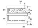
- FIG. 1 is an explanatory diagram of the entire liquid crystal display system 900 according to the present embodiment.
- the liquid crystal display panel 100 is used as the image display panel.
- a liquid crystal display system 900 includes a liquid crystal display panel 100 that displays an image during normal use, a backlight 300 that irradiates illumination light to the back side of the liquid crystal display panel 100, and the liquid crystal display panel 100.
- Backlight control for controlling an on / off state of a light scattering liquid crystal display panel 200 in which a light scattering liquid crystal layer is sandwiched between substrates, a liquid crystal control unit 500, and a backlight 300, which display an image when not in use.
- Part 501 The liquid crystal controller 500 controls the liquid crystal state of the liquid crystal display panel 100 and the light scattering liquid crystal display panel 200.
- the backlight control unit 501 turns on the backlight 300 in the first state, and turns off the backlight 300 in the second state.
- FIG. 2 is a cross-sectional view of the liquid crystal display system 900 according to the present embodiment.
- the light-scattering liquid crystal display panel 200 is, for example, an active matrix liquid crystal display panel, and is opposed to the first transparent substrate 11 and the first transparent substrate 11 disposed on the front side. It has the 2nd transparent substrate 12 arrange
- the 2nd transparent substrate 12 arrange
- the memory liquid crystal of the memory liquid crystal layer 36 is not particularly limited.
- a ferroelectric liquid crystal or a cholesteric liquid crystal having excellent memory characteristics can be used.
- a counter electrode 25 is formed as a first electrode on the inner side of the first transparent substrate 11, that is, the back surface, and a pixel electrode 23 is formed as a second electrode on the inner side, that is, the front surface of the second transparent substrate 12. Is done.
- the counter electrode 25 is given a predetermined counter potential from an external drive circuit (not shown).
- a liquid crystal display panel 100 is disposed on the back side of the light scattering liquid crystal display panel 200.
- the liquid crystal display panel 100 is also an active matrix type liquid crystal display panel, for example, and includes a third transparent substrate 13 disposed on the front side and a fourth transparent substrate 14 disposed on the back side facing the third transparent substrate 13. And a liquid crystal layer 26 sandwiched between the third transparent substrate 13 and the fourth transparent substrate 14.
- the third transparent substrate 13 of the liquid crystal display panel 100 and the second transparent substrate 12 of the light scattering liquid crystal display panel 200 are disposed to face each other.
- the liquid crystal layer 26 is not particularly limited.
- a TN (twistedistnematic) type, a GH (guest-host) type, an STN (super-twisted nematic) type, an SBE (super-twistedbirefringence effect) type, An ECB (electrically controlled birefringence) type or the like can be used.
- a counter electrode 35 is formed as a third electrode on the inner side of the third transparent substrate 13, that is, the back surface, and a pixel electrode 33 is formed as a fourth electrode on the inner side, that is, the front surface of the fourth transparent substrate 14. Is done. A predetermined counter potential is applied to the counter electrode 35 from an external drive circuit (not shown). On the outside of the third transparent substrate 13 and the fourth transparent substrate 14, a normal absorption type upper polarizing plate 32 and a lower polarizing plate 31 arranged in crossed Nicols are formed.
- substrate which has light transmittances such as a glass plate and a quartz plate, is used. can do.
- the pixel electrodes 23 and 33 and the counter electrodes 25 and 35 are made of a light transmissive conductive material such as ITO (indium tin oxide).
- the liquid crystal display panel 100 and the light-scattering liquid crystal display panel 200 are arranged with a predetermined interval through, for example, a spacer, but are not limited thereto, and the liquid crystal display panel 100 and the light-scattering liquid crystal display panel 200 are arranged.
- the second transparent substrate 12 of the light-scattering liquid crystal display panel 200 and the third transparent substrate 13 of the liquid crystal display panel 100 can be disposed in close contact with each other.
- a backlight 300 is disposed on the back side of the liquid crystal display panel 100.
- the backlight 300 is formed with, for example, a plurality of light emitting units, and specifically is an illumination unit in which a plurality of fluorescent tubes are arranged, for example.
- the plurality of fluorescent tubes constituting the backlight 300 are formed so as to extend over the entire width direction of the liquid crystal display panel 100, and almost the entire vertical direction of the liquid crystal display panel 100 along a plane parallel to the liquid crystal display panel 100. It is held by a lamp holder (not shown) in a state of being arranged over.
- the fluorescent tube of the backlight 300 is not particularly limited, and for example, a cold cathode tube, a hot cathode tube, or the like can be used. Moreover, a light bulb can be used instead of a fluorescent tube.
- the liquid crystal control unit 500 shown in FIG. 1 forms an image on the liquid crystal display panel 100 (first state)
- an electric field is formed between the pixel electrode 23 and the counter electrode 25 to cause the memory liquid crystal layer 36 to light.
- the transmissive state the image formed on the liquid crystal display panel 100 is transmitted through the memory liquid crystal layer 36 and displayed on the light scattering liquid crystal display panel 200.
- the liquid crystal control unit 500 uses the pixel electrode 23 and the counter electrode 25 at predetermined positions on the light-scattering liquid crystal display panel 200.
- An electric field is formed between the two electrodes to make the memory liquid crystal layer 36 in a light-transmitting state and display a dark color, and at other locations on the light-scattering liquid crystal display panel 200, an electric field is not formed between the two electrodes.
- the liquid crystal layer 36 is in a light scattering state to scatter outside light, thereby performing bright color display, and displaying a bright and dark image composed of a combination of the bright color display and the dark color display on the light scattering liquid crystal display panel 200.
- the liquid crystal control unit 500 puts the liquid crystal layer 26 of the liquid crystal display panel 100 into a light non-transmissive state in order to prevent light from the back side of the liquid crystal display panel 100 from passing through the liquid crystal layer 26.
- the configuration of the liquid crystal display system 900 is not limited to the configuration including four transparent substrates, and as shown in FIG. 3, the third transparent substrate of the image display panel 100 and the light scattering.
- the second transparent substrate of the liquid crystal display panel 200 can also be configured as one common transparent substrate 15.
- the pixel electrode 23 is formed on the front surface of the common transparent substrate 15, and the counter electrode 35 is formed on the rear surface of the common transparent substrate 15. Is formed. According to this configuration, it is possible to prevent a decrease in light transmittance due to the overlapping of a plurality of transparent substrates, and it is possible to reduce the thickness of the liquid crystal display system. Can match.
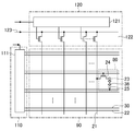
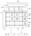
- FIG. 4 is an active matrix circuit configuration diagram of the light-scattering liquid crystal display panel 200.
- the light scattering liquid crystal display panel 200 includes a display unit 90 in which a plurality of display pixels 80 are formed, a scanning line driving circuit 110, and a signal line driving circuit 120.
- the scanning line driving circuit 110 and the signal line driving circuit 120 are formed integrally with the signal line 21, the scanning line 22, and the pixel electrode 23 on the second transparent substrate 12.
- a plurality of scanning lines 22 and a plurality of signal lines 21 intersecting with the scanning lines 22 are arranged on the second transparent substrate 12 in a matrix shape via an insulating film (not shown).
- display pixels 80 are arranged at each intersection of the scanning lines 22.
- the display pixel 80 includes a pixel electrode 23, a thin film transistor (TFT) 24, a counter electrode 25, and a memory liquid crystal layer 36.
- the source of the thin film transistor 24 is connected to the signal line 21, the gate is connected to the scanning line 22, and the drain is connected to the pixel electrode 23.
- the scanning line driving circuit 110 includes a buffer circuit, a shift register 111, and the like (not shown), and sequentially outputs scanning signals to the scanning line 22 based on a control signal supplied from an external driving circuit (not shown). I will do it. For example, when a moving image such as a clock display is displayed on the light-scattering liquid crystal display panel 200, the scanning line driving circuit 110 sets the control signal line 30 to the off level, and sequentially in the same manner as in a normal active matrix liquid crystal display panel. A scanning signal is output to the scanning line 22. On the other hand, when displaying still images such as various weather marks such as sunny, rain, snow, etc. on the light-scattering liquid crystal display panel 200, for example, the scanning line 22 is turned off and the control signal line 30 is turned on. Level.
- the signal line driving circuit 120 includes an analog switch 122, a shift register 121, and the like, and a video signal is supplied from an external driving circuit (not shown) through a control signal and a video bus 123.
- the signal line driver circuit 120 samples the video signal supplied from the video bus 123 on the signal line 21 at a predetermined timing by supplying an open / close signal of the analog switch 122 from the shift register 121.
- the active matrix circuit configuration of the liquid crystal display panel 100 is formed in the same manner as the active matrix circuit configuration of the light scattering liquid crystal display panel 200 described above. That is, the display unit includes a display unit in which a plurality of display pixels are formed, a scanning line driving circuit, and a signal line driving circuit.
- the scanning line driving circuit and the signal line driving circuit are arranged on the fourth transparent substrate 14.
- the signal line, the scanning line, and the pixel electrode 33 are integrally formed.
- a plurality of scanning lines and a plurality of signal lines intersecting with the scanning lines are arranged in a matrix shape through an insulating film, and display pixels are arranged at the intersections of the signal lines and the scanning lines. Are arranged, and the display unit is configured by including the display pixels.
- the display pixel includes a pixel electrode 33, a thin film transistor, a counter electrode 35, and a liquid crystal layer 26.
- the source of the thin film transistor is connected to the signal line, the gate is connected to the scanning line, and the drain is connected to the pixel electrode.
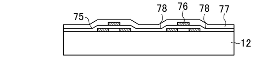
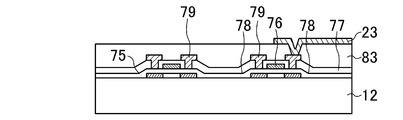
- FIG. 5A to 5F are schematic views of the manufacturing process of the liquid crystal display system 900.
- FIG. 5A an amorphous silicon thin film 71 is deposited on a second transparent substrate 12 such as glass by a plasma CVD method, and this amorphous silicon thin film 71 is annealed by a laser device to be polycrystallized.
- the laser beam 72 from the laser device is scanned in the direction of the arrow in the drawing, and the region irradiated with the laser beam 72 is crystallized to become a polycrystalline silicon film 73.
- FIG. 5A an amorphous silicon thin film 71 is deposited on a second transparent substrate 12 such as glass by a plasma CVD method, and this amorphous silicon thin film 71 is annealed by a laser device to be polycrystallized.
- the laser beam 72 from the laser device is scanned in the direction of the arrow in the drawing, and the region irradiated with the laser beam 72 is crystallized to become a polycrystalline
- the polycrystalline silicon film 73 is patterned by photolithography to form an active layer 74 of the thin film transistor.
- a gate insulating film 75 made of a silicon oxide film is formed by plasma CVD, and then a Mo—W alloy film is formed by sputtering and patterned to form a gate electrode 76. Scan lines are also formed simultaneously during patterning.
- impurities are implanted by ion doping using the gate electrode 76 as a mask to form a source / drain region 78 of the thin film transistor.
- a first interlayer insulating film 77 made of a silicon oxide film is formed on the gate electrode 76 by plasma CVD.
- FIG. 5E after forming contact holes in the first interlayer insulating film 77 and the gate insulating film 75, an aluminum film is formed by sputtering and patterned to form source / drain electrodes 79. At this time, a signal line is also formed.
- FIG. 5F a second interlayer insulating film 83 is formed on the aluminum film. Then, a contact hole is formed in the second interlayer insulating film 83, and a pixel electrode 23 is further formed.
- gate electrodes, source / drain electrodes, scanning lines, and signal lines are formed on the front side, and a counter electrode 25 is formed on the back side by sputtering or the like.
- a first transparent substrate is prepared.
- the first transparent substrate 11 and the second transparent substrate 12 are opposed to each other, the periphery is sealed with a sealing material 29, the composition of the memory liquid crystal layer 36 is injected therein, and the light scattering liquid crystal is sealed therein.
- a display panel 200 is formed.
- the third transparent substrate 13 and the fourth transparent substrate 14 are opposed to each other, the periphery is sealed with a sealing material 39, and the liquid crystal layer is contained inside.
- the liquid crystal display panel 100 is formed by injecting and sealing 26 compositions.
- the liquid crystal display system 900 is manufactured by arranging the second transparent substrate 12 of the light-scattering liquid crystal display panel 200 and the third transparent substrate 13 of the liquid crystal display panel 100 to face each other.
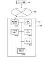
- FIG. 6 is a block diagram of a digital signage system 400 via the Internet.
- the digital signage system 400 includes a digital signage device 410 in which the liquid crystal display system 900 according to the present invention is used as a display device, and a dedicated server device 421 connected via the Internet 420. Configured.
- the electronic signboard device 410 is a device that is installed at an entrance of a store or a company and displays contents such as advertisements and information for employees.
- the communication circuit control unit 411 connects the electronic signboard device 410 to the server device 421 via the Internet 420.
- the provided content is automatically distributed from the server device 421, or a predetermined URL is input from the URL memory 414 by operating the electronic signage device 410, or manually input from the operation unit 415, and the dedicated server device Connect to 421 to receive content.
- the received content data is stored in the received data memory 412 in a temporary drop.
- the browser memory 413 stores browser software that generates predetermined display screen contents from the received content.
- the operation unit 415 is operated to select and read necessary content from the reception data memory 412, and a display screen signal is generated from the content data and displayed on the liquid crystal display system 900.
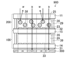
- FIG. 7A and 7B are cross-sectional views illustrating a usage mode of the liquid crystal display system 900.
- FIG. 7A shows a normal display mode (first state) for forming an image on the liquid crystal display panel 100
- FIG. 7B shows a display mode (second state) for forming an image on the light-scattering liquid crystal display panel 200. .
- the liquid crystal control unit 500 when displaying the content distributed from the server device 421 on the liquid crystal display panel 100 of the liquid crystal display system 900, the liquid crystal control unit 500 applies a voltage between the pixel electrode 23 and the counter electrode 25. When applied, the liquid crystal molecules 38 in the memory liquid crystal layer 36 are brought into an aligned state, thereby changing the memory liquid crystal layer 36 of the light-scattering liquid crystal display panel 200 to a light transmissive state.
- the backlight control unit 501 turns on the backlight 300. As a result, the content displayed on the liquid crystal display panel 100 passes through the light scattering liquid crystal display panel 200 and is recognized by the customer.
- the liquid crystal control unit 500 causes the light scattering liquid crystal display panel 200 to
- the liquid crystal molecules 38 in the memory liquid crystal layer 36 are set in a random state without forming an electric field between the pixel electrode 23 and the counter electrode 25 at a predetermined location, and the memory liquid crystal layer 36 of the light-scattering liquid crystal display panel 200 is changed to a light scattering state.
- bright light display for example, white display W
- white display W is performed at a predetermined position on the light-scattering liquid crystal display panel 200 by scattering external light.
- a voltage is applied between the pixel electrode 23 and the counter electrode 25 to align the liquid crystal molecules 38 in the memory liquid crystal layer 36.
- a dark color display (for example, black display B) is performed on the light scattering liquid crystal display panel 200 by changing the memory liquid crystal layer 36 to an aligned state and a light transmitting state.
- the liquid crystal control unit 500 puts the liquid crystal layer 26 of the liquid crystal display panel 100 into a light non-transmissive state.
- the backlight control unit 501 turns off the backlight 300.
- an image composed of a combination of the light color display and the dark color display is formed on the light scattering liquid crystal display panel 200.
- the images that can be displayed on the light-scattering liquid crystal display panel 200 are letters, numbers, symbols, figures, or a combination thereof.
- Embodiment 2 In Embodiment 1 described above, when the liquid crystal display panel 100 is not used, the backlight 300 is turned off and an image composed of a combination of bright color display and dark color display is displayed on the light scattering liquid crystal display panel 200.
- the present invention is not limited to such an embodiment.
- the backlight control unit 501 when the liquid crystal display panel 100 is not used (second state), the backlight control unit 501 does not turn off the backlight 300, but uniformly turns on the whole in a low power consumption state. .
- the backlight control unit 501 can turn on a part of the light emitting unit and turn off the other part.
- an image composed of a combination of bright color display and dark color display can be displayed on the light scattering liquid crystal display panel 200 while saving power consumption.
- FIG. 8 is a diagram for explaining a display form in which the backlight 300 corresponding to the place where the dark color display is formed is turned off and the backlight 300 is turned on at the position corresponding to the place where the bright color display is formed.
- the liquid crystal display system 900 is configured with the three transparent substrates shown in FIG. 3 will be described as an example. As shown in FIG.
- the backlight control unit 501 turns off the light emitting unit of the backlight 300 corresponding to the location where the dark color display (for example, black display B) is formed on the light scattering liquid crystal display panel 200, On the other hand, the light emitting part of the backlight 300 corresponding to the place where the bright color display (for example, white display W) is formed on the light scattering liquid crystal display panel 200 is turned on.
- the liquid crystal controller 500 keeps the liquid crystal layer 26 of the liquid crystal display panel 100 in a light transmissive state.
- the liquid crystal molecules 38 in the memory liquid crystal layer 36 are changed to a random state, and the memory liquid crystal layer 36 is changed to a light scattering state, thereby Even if the light color display is performed by scattering the light, the intensity of the scattered light is lowered and the light color display may be weakened. Therefore, by turning on the light emitting portion of the backlight 300 corresponding to the place where the bright color display is formed, the light of the backlight 300 is scattered by the liquid crystal molecules 38 in the random state, and scattered light is generated. Thus, the contrast between the light color display and the dark color display can be enhanced by supplementing the light color display.
- FIG. 9 is a diagram for explaining a liquid crystal display system 900 in which a color filter layer is formed on the back inner side of the first transparent substrate 11.
- the color filter layer is formed of R (red) 51, G (green) 52, and B (blue) 53, and the black matrix BM is divided into the third transparent substrate 13 so as to partition each pixel.
- R (red) 51, G (green) 52, and B (blue) 53 are formed between the black matrixes BM.
- R (red) 51, G (green) 52, and B (blue) 53 are formed using a photosensitive colored resist, and the arrangement is a stripe pattern.
- no color filter layer is formed inside the back surface of the common transparent substrate 15. This is because if the color filter layer is also formed inside the back surface of the common transparent substrate 15, the light transmittance is deteriorated and the transparency is lowered.
- a black matrix is provided inside the common transparent substrate 15 so as to partition each pixel, and R (red), G (green), and B (blue) are provided between the black matrices. ) Can also be formed. In such a case, a color filter is not formed inside the fourth transparent substrate 14 in order to prevent the light transmittance from being lowered.
- the color filter layer is formed inside the first transparent substrate, and the color filter layer is formed inside the back surface of the third transparent substrate 13. Is not formed. It is also possible to form the color filter layer inside the front surface of the second transparent substrate and not form the color filter layer inside the front surface of the fourth transparent substrate 14.
- Embodiment 5 In Embodiment 4 described above, the color filter layer having a different color for each pixel is formed. However, when performing color display, the present invention is not limited to such an embodiment.
- color display is performed by mixing a dye into the memory liquid crystal layer 36.
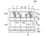
- FIG. 10A shows a case where the emitted light of the mixed dye is absorbed
- FIG. 10B shows a case where the emitted light of the mixed dye is irradiated to the outside.
- the liquid crystal display system 900 is configured with the three transparent substrates shown in FIG. 3 will be described as an example.
- the mixed dye is, for example, a green dye
- the green light 160 when no electric field is formed on the memory liquid crystal layer 36, the green light 160 is absorbed by the green dye mixed in the liquid crystal molecules as shown in FIG. 10A. Although not emitted in the viewing direction, the emitted light 161 other than the green light is not absorbed by the green dye, but is scattered by the green dye mixed in the liquid crystal molecules, so that a display with an enlarged viewing angle can be obtained.
- the green light 160 is emitted without being absorbed by the pigment, and the emitted light 161 other than the green light is also mixed into the liquid crystal molecules. Since the green pigment is scattered and emitted without being absorbed, all incident light is emitted and becomes white light.
- color display can be performed by mixing red, green, and blue primary color pigments for each pixel.
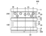
- FIG. 11A and FIG. 11B are diagrams for explaining an embodiment in which the viewing angle dependency is made variable while an image is displayed on the light-scattering liquid crystal display panel 200.
- FIG. 11A shows a case where display with little visual dependency is performed
- FIG. 11B shows a case where display with high visual dependency is performed.
- the liquid crystal display system 900 is configured with the three transparent substrates shown in FIG. 3 will be described as an example.
- an electric field is formed with respect to the memory liquid crystal layer 36 in the case of performing display with a high visual dependence (when displaying with a narrow viewing angle). Since the liquid crystal molecules are aligned substantially parallel to the electric field by the applied electric field, the emitted light is emitted as it is without being scattered by the liquid crystal molecules. Therefore, for example, in the case where the liquid crystal display system 900 according to the present embodiment is used as a digital signage display device, when displaying to a small number of customers, it is advantageous because the luminance and contrast ratio can be increased. .
- the external light applied to the display unit 90 of the light-scattering liquid crystal display panel 200 may have different intensity depending on the region. In such a case, it is difficult to provide a good display. For example, in some areas of the display unit 90, since the intensity of external light is high, bright color display due to external light scattering is emphasized, while in other areas, bright color display due to external light scattering is normal. There is. Therefore, in the seventh embodiment, a plurality of optical sensors are arranged in the display unit 90, the intensity of external light in the display unit 90 is detected for each predetermined region, and the external light irradiation state is determined based on the detection result. Good display.
- FIG. 12 is a block diagram of a configuration in which a plurality of optical sensors are arranged in the display unit 90 of the light-scattering liquid crystal display panel 200.
- the display unit 90 is provided with an optical sensor 180 for each predetermined region, and the intensity of external light irradiated on the display unit 90 can be detected for each predetermined region.
- a total of x.times.y lights in each of the x.times.y regions obtained by dividing the horizontal direction (horizontal direction) of the display unit 90 into x pieces and dividing the vertical direction (vertical direction) into y pieces.
- a sensor 180 is provided.
- one optical sensor 180 is provided for each pixel formation portion, and the optical sensor 180 is provided for each region corresponding to one pixel in the display unit 90.
- the image correction unit 510 corrects the image displayed on the display unit 90 according to the distribution of the intensity of external light on the display unit 90 based on the detection result by the optical sensor 180.
- a data signal representing an image to be displayed is given to the liquid crystal display unit 500 as an input signal from the outside.
- Detection values indicating external light intensity obtained by the optical sensor 180 in each region of the display unit 90 are input to the image correction unit 510.
- the image correction unit 510 corrects the image signal corresponding to the data signal from the outside based on the detected value of the external light intensity. That is, in a region where the intensity of external light is high, the liquid crystal molecules 38 in the memory liquid crystal layer 36 are changed from a random state to a slightly light-transmitting alignment state.
- the slight alignment in the light transmission state means that the light transmittance when the liquid crystal molecules are in a random state is T 1 %, and the light transmission alignment state is T 2 % (where T 2 > T 1 ), although not particularly limited, for example, the transmittance is [T 1 +0.2 (T 2 ⁇ T 1 )]% to [T 1 +0.4 (T 2 ⁇ T 1 )]. %.
- the liquid crystal molecules 38 are aligned in a slight light transmission state even in a region where the intensity of the external light is high, so that the color is slightly dark and the bright color display can be prevented from being emphasized. Therefore, even if the external light intensity varies depending on the position on the display unit 90, the customer can visually recognize an image in which the original contrast is maintained on the entire screen.
- a plurality of optical sensors 180 are arranged in the display unit 90 to detect the intensity of external light in the display unit 90 for each predetermined region, and in a region where the external light intensity is high, the liquid crystal molecules 38. was changed so as to be oriented from a random state to a slightly light transmissive state, thereby suppressing the emphasis of bright color display and visually recognizing an image maintaining the original contrast.
- the scope of the present invention is not limited to such an embodiment. For example, in some areas of the display unit 90, since the intensity of external light is low, the bright color display due to scattered light may be weakened.
- a plurality of photosensors 180 are arranged in the display unit 90 of the liquid crystal display panel 100, and in each region of the display unit 90, the external light intensity is obtained by the photosensor 180.
- control is performed so that the light emitting unit of the backlight 300 corresponding to the region is turned on.
- the liquid crystal controller 500 keeps the liquid crystal layer 26 of the liquid crystal display panel 100 in a light transmissive state. Thereby, the light of the backlight 300 is scattered by the liquid crystal molecules 38 in a random state to generate scattered light. Therefore, the contrast between the bright display and the dark display can be enhanced by supplementing the bright display.
- FIG. 13 is an explanatory diagram of a liquid crystal display panel system 900 in which the reflector plate 40 is formed.
- the reflecting mirror plate 40 is formed in a region that is not a region for forming a light transmission state in the memory liquid crystal layer 36 of the light-scattering liquid crystal display panel 200.
- the region that is not the region that forms the light transmission state is a region that does not contribute to the light transmission state, and is not particularly limited, but is, for example, the upper portion of the wiring on the pixel.
- the black matrix BM does not transmit light and does not contribute to the light transmission state
- the region immediately below the black matrix BM is a region that is not a region that forms a light transmission state.
- the reflecting mirror plate 40 is disposed in a region directly below the black matrix BM and inside the front surface of the common transparent substrate 15.
- the liquid crystal controller 500 brings the liquid crystal layer 26 of the liquid crystal display panel 100 into a light non-transmissive state.
- the backlight control unit 501 turns off the backlight 300.
- the liquid crystal molecules 38 in the memory liquid crystal layer 36 are set in a random state, and the memory liquid crystal layer 36 of the light-scattering liquid crystal display panel 200 is changed into a light scattering state.
- light color display for example, white display W
- the incident light 164 that has entered the vicinity of the pixel electrode 23 without being scattered by the liquid crystal molecules 38 is reflected by the reflecting mirror plate 40 and is scattered by the liquid crystal molecules 38, thereby performing bright color display.
- the incident light 162 is incident on the light-transmitting memory liquid crystal layer 36 and is not reflected, resulting in dark color display (for example, black display B). Thereby, even when the intensity of external light is low, it is possible to enhance the bright color display and maintain the contrast ratio of the image.
- the liquid crystal display panel 100 is used as the image display panel.
- the present invention is not limited to such an embodiment, and examples of the image display panel include an organic EL display panel and an inorganic display panel.
- the usage example of the liquid crystal display system 900 according to the above embodiment is not limited to digital signage.
- the liquid crystal display system according to the present invention can display an image with low power consumption even when the image display panel is turned off, the liquid crystal display system is suitably used for advertisement display such as digital signage.
Landscapes
- Engineering & Computer Science (AREA)
- Physics & Mathematics (AREA)
- Computer Hardware Design (AREA)
- General Physics & Mathematics (AREA)
- Theoretical Computer Science (AREA)
- Chemical & Material Sciences (AREA)
- Crystallography & Structural Chemistry (AREA)
- Control Of Indicators Other Than Cathode Ray Tubes (AREA)
- Liquid Crystal Display Device Control (AREA)
Abstract
画像表示パネルが電源オフ状態の場合でも、情報表示を可能とする液晶表示システムを提供する。液晶表示パネル100と、メモリ液晶層36を電極間に有する光散乱性液晶表示パネル200とを有する。液晶表示パネル100を使用する際は、光散乱性液晶表示パネル200のメモリ液晶層36を光透過状態に変化させる。一方、液晶表示パネル100を使用しない際は、メモリ液晶層36の所定箇所にて光散乱状態の画素を形成して明色表示を行い、メモリ液晶層36の他の箇所にて光透過状態の画素を形成して暗色表示を行い、該明色表示及び暗色表示の組み合わせから成る画像を光散乱性液晶表示パネル上に形成する。
Description
本発明は、デジタルサイネージ等に使用される液晶表示システム、及びその液晶表示システムの制御方法に関する。
近年、デジタル技術の発展に伴い、屋外や店舗等でハイビジョン画質等の高画質の映像を画像表示パネルのディスプレイで再生することにより宣伝を行う、特許文献1及び2に示すようなデジタルサイネージと呼ばれるシステムが存在する。
デジタルサイネージでは、ネットワーク等を使うことにより画像表示パネルに動画や静止画を配信し表示することにより、広告配信等を行うことができる。このデジタルサイネージのディスプレイには、薄型、軽量、低消費電力という利点があるので、画像表示パネルとしては例えば液晶表示パネルがよく使われる。
しかし、一般的なデジタルサイネージシステムでは、広告配信を行っていない場合は、消費電力の省力化のため画像表示パネルを電源オフ状態にして何も表示しない。そのため画像表示パネルのディスプレイに情報表示がなされておらず宣伝、広告機能が不十分である。
そこで画像表示パネルが電源オフ状態のときでも、ディスプレイに所定の文字や絵、模様等を表示しておくことができるように、液晶を挟持した一対の基板を備え、その一対の基板に光反射領域及び光透過領域を有するサブ画素が複数形成された表示領域を有している液晶表示装置が特許文献3に記載されている。
この液晶表示装置は、複数のサブ画素の各々の光反射領域及び光透過領域が互いに独立して駆動するように構成されており、電源オフ時に、光反射領域を一旦直流駆動して特定画像を表示した後に電源オフ状態とすることで、電源オフ時でもディスプレイに特定画像が継続して表示される。
しかし、この液晶表示装置では、電源オフ時にディスプレイに同一の画像が継続して表示されるにすぎないので、宣伝・広告等の情報伝達媒体として十分に利用できるものではない。
本発明はかかる問題点に鑑みてなされたものであって、画像表示パネルを電源オフ状態にして消費電力が省力化されている場合でも、宣伝・広告等の伝達媒体として十分に利用できる情報表示を可能とする液晶表示システムを提供することを目的とする。
上記目的を達成するために、本発明では、画像を形成する画像表示パネルと、光散乱液晶層を電極間に有する光散乱性液晶表示パネルとを重ねて液晶表示システムを形成する。そして、画像表示パネルにて画像を形成しない場合は、光散乱状態の画素を形成して入射光を散乱させることにより光散乱性液晶表示パネル上の所定の箇所に明色表示を行うと共に、光透過状態の画素を形成して暗色表示を光散乱性液晶表示パネル上の他の箇所に行うことにて、これら明色表示及び暗色表示の組み合わせから成る明暗画像を光散乱性液晶表示パネル上に形成する。
具体的には、本発明の第1の観点に係る液晶表示システムは、第1電極を有し正面側に配置される第1透明基板、第2電極を有し背面側に配置される第2透明基板、及び、前記第1電極と前記第2電極とが対向するように前記第1透明基板と前記第2透明基板とを配置してその間に封止された光散乱性液晶層、を有して構成された光散乱性液晶表示パネルと、前記光散乱性液晶表示パネルの背面側に配置され、画像を形成する画像表示パネルと、液晶の配向状態を制御する液晶制御部と、を備え、前記液晶制御部は、前記画像表示パネルにて画像を形成する第1状態の場合は、前記光散乱性液晶表示パネルにて第1電極と第2電極の間に電界を形成して光散乱性液晶層を光透過状態にし、前記画像表示パネルで形成された画像を光散乱性液晶層を透過させて前記光散乱性液晶表示パネル上に表示し、一方、前記画像表示パネルにて画像を形成しない第2状態の場合は、前記光散乱性液晶表示パネル上の所定箇所にて第1電極及び第2電極の両電極間に電界を形成して光散乱性液晶層を光透過状態にして暗色表示を行うと共に、光散乱性液晶表示パネル上の他の箇所では該両電極間に電界を形成しないことで光散乱性液晶層を光散乱状態にして外光を散乱させることにより明色表示を行い、該明色表示及び暗色表示の組み合わせから成る明暗画像を前記光散乱性液晶表示パネル上に表示することを特徴とする。
ここで、明色表示とは、散乱光に基づいて認識される色彩表示であり、例えば白色表示である。暗色表示とは、外光が配向状態の光散乱性液晶層を通過して反射されないことに基づいて認識される色彩表示であり、例えば黒色表示や灰色表示である。
また、光散乱性液晶層とは、電圧が印加されていない時には、液晶分子の配向状態がランダムになっており、入射光を散乱させて白濁して見え(液晶シャッターが閉じた状態)、一方、電圧が印加されている時には、液晶分子が電界に対して平行に配向して光を透過する(液晶シャッターが開いた状態)挙動を有する液晶層である。
この構成によれば、画像表示パネルが電源オフ状態の場合でも、光散乱性液晶表示パネル上に、光散乱状態の画素を形成して所定の箇所に明色表示を行うと共に、光透過状態の画素を形成して暗色表示を他の箇所に行うことにより、これら明色表示及び暗色表示の組み合わせから成る明暗画像を光散乱性液晶表示パネル上に形成することができるので、消費電力の省力化を行いつつも、光散乱性液晶表示パネル上に種々の静止画又は動画を表示できるため宣伝、広告機能を十分に果たすことができる。
また、前記画像表示パネルは、第3電極が配置された第3透明基板、第4電極が配置された第4透明基板、及び、前記第3電極と前記第4電極とが対向するように前記第3透明基板と前記第4透明基板とを配置してその間に封止された液晶層、を有して構成された液晶表示パネルであり、前記液晶表示パネルの第3透明基板と、前記光散乱性液晶表示パネルの第2透明基板とは対向して配置されていることも可能である。この構成によれば、低消費電力かつ薄型に画像表示パネルを構成することができる。
また、前記液晶制御部は、前記第2状態の場合、前記液晶表示パネルの液晶層を光非透過状態にすることが好ましい。
この構成によれば、第2状態の場合、液晶表示パネルの液晶層を光非透過状態にするので、液晶表示パネルの背面側からの光が液晶表示パネルを通過せず、そのため光散乱性液晶表示パネル上の所定箇所に形成される暗色表示をクリアに表示できる。
また、前記液晶表示パネルの背面側に照明光を照射するバックライトと、前記バックライトの点灯及び消灯状態を制御するバックライト制御部と、を有し、前記バックライト制御部は、前記第1状態の場合は前記バックライトを点灯させ、一方、前記第2状態の場合は、前記バックライトを消灯させるか、又は、低消費電力状態で点灯させることが好ましい。ここでバックライトを低消費電力状態で点灯させるとは、バックライトの発光部を薄暗く点灯させて消費電力を低く抑えることをいう。
この構成によれば、第1状態の場合はバックライトの照明により画像を明るく表示することができ、一方、第2状態の場合は、バックライトを消灯又は低消費電力状態で点灯させるので、消費電力の省力化を達成することができる。
また、前記液晶表示パネルの背面側に照明光を照射する複数の発光部を有するバックライトと、前記バックライトの点灯及び消灯状態を制御するバックライト制御部と、を有し、前記バックライト制御部は、前記第1状態の場合は、前記バックライトを点灯させ、一方、前記第2状態の場合は、該発光部の一部を点灯させ、他の一部を消灯させることが好ましい。この構成においても、第2状態の場合は、バックライトの一部しか点灯していないので、消費電力の省力化を達成することができる。
また、前記液晶表示パネルの背面側に照明光を照射する複数の発光部を有するバックライトと、前記バックライトの点灯及び消灯状態を制御するバックライト制御部と、を有し、前記液晶制御部は、前記第2状態の場合、前記液晶表示パネルの液晶層を光透過状態にし、前記バックライト制御部は、前記第2状態において、前記光散乱性液晶表示パネルの暗色表示が形成される箇所に対応するバックライトの発光部を消灯状態とし、一方、明色表示が形成される箇所に対応するバックライトの発光部を点灯状態とすることも可能である。
光散乱性液晶表示パネルに照射される外光の強度が全体として低い場合は、散乱光による明色表示がぼんやりとなるためコントラスト比が弱まる可能性があるが、この構成によれば、外光の強度が低い場合であっても、明色表示が形成される箇所に対応するバックライトの発光部を点灯状態とすることにより、バックライトの光はランダム状態の液晶分子にて散乱されて散乱光を生じ、これにより明色表示を補うことで明色表示と暗色表示とのコントラストを強調させることができる。
また、前記液晶表示パネルの背面側に照明光を照射する複数の発光部を有するバックライトと、前記バックライトの点灯及び消灯状態を制御するバックライト制御部と、マトリクス状に配置された複数の表示画素からなる表示部における外光の強度を所定領域毎に検出する複数の光センサと、を有し、前記液晶制御部は、前記第2状態の場合、前記液晶表示パネルの液晶層を光透過状態にし、前記光センサより、前記光散乱性液晶表示パネルに照射される外光の強度が他の領域よりも低いと検出された領域では、前記バックライト制御部は、該領域に対応する発光部を点灯させることも可能である。
光散乱性液晶表示パネルに照射される外光の強度が一部において低い領域がある場合は、その領域における明色表示が他の領域よりもぼんやりとなりコントラスト比が他の領域よりも異なる可能性があるが、この構成によれば、外光の強度が低い領域でもその領域に対応するバックライトの光を照射してランダム状態の液晶分子にて散乱させて、明色表示を補うことで明色表示と暗色表示とのコントラストを強調させることができる。
また、マトリクス状に配置された複数の表示画素からなる表示部における外光の強度を所定領域毎に検出する複数の光センサと、前記光センサによる検出結果に基づいて、外光の強度の前記表示部における分布に応じて前記表示部に表示される画像を補正する画像補正部と、を有することも可能である。
光散乱性液晶表示パネルに照射される外光の強度が一部において高い領域がある場合は、その領域における明色表示が他の領域よりも強調されてコントラスト比が他の領域よりも異なる可能性があるが、この構成によれば、外光の強度が高い領域がある場合でもその領域の液晶分子を若干の光透過状態に配向させるので若干暗色状態になり、明色表示の強調を抑制させることができる。従って、表示部上の位置によって外光強度が異なったとしても、顧客には画面全体で本来のコントラストが維持された画像が視認される。
また、前記光散乱性液晶表示パネルの光散乱性液晶層における光透過状態を形成する領域ではない領域に、前記光透過性液晶層内に進入した外光を反射させて該散乱性液晶層内で散乱させる反射鏡板を形成することが好ましい。
光散乱性液晶表示パネルの散乱性液晶層内には、例えば画素上の配線の上部や、例えばブラックマトリクスの直下の領域のように光透過状態に寄与しない領域がある。その領域に進入した外光を反射させる反射鏡板を形成することにより、散乱性液晶層内に進入した外光を反射鏡板により散乱性液晶層に反射させて該散乱性液晶層内で散乱させ、明色表示を強調するため、より光散乱性液晶表示パネル上に形成される画像のコントラストを鮮明にさせることができる。
また、前記第1透明基板の背面内側に画素毎に色が異なるカラーフィルター層を形成すると共に、前記第3透明基板の背面内側にはカラーフィルター層を形成しないことも可能である。
この構成によれば、第1透明基板の背面内側にカラーフィルター層を形成しているため、画像表示パネルにて画像を形成する第1状態の場合において、光散乱性液晶表示パネル上に表示される画像をカラーにて表示させることでき、宣伝及び広告機能を十分に果たすことができる。更に、第3透明基板の背面内側にはカラーフィルターを形成していないため、カラーフィルターを重ねて設けることに起因する透過性の低下を防止することができる。
また、前記第2透明基板の正面内側に画素毎に色が異なるカラーフィルター層を形成すると共に、前記第4透明基板の正面内側にはカラーフィルター層を形成しないことも可能である。
この構成によれば、第2透明基板の正面内側にカラーフィルター層を形成しているため、画像表示パネルにて画像を形成する第1状態の場合において、光散乱性液晶表示パネル上に表示される画像をカラーにて表示させることでき、宣伝及び広告機能を十分に果たすことができる。更に、第4透明基板の正面内側にはカラーフィルターを形成していないため、カラーフィルターを重ねて設けることに起因する透過性の低下を防止することができる。
また、前記光散乱性液晶層中に色素を混入することも可能である。
この構成によれば、画像表示パネルにて画像を形成する第1状態の場合において、光散乱性液晶表示パネルの光散乱性液晶層を光散乱状態又は光透過状態に制御することによりカラー表示を行うことができる。例えば光散乱性液晶層中に緑色の色素を混入した場合、光散乱性液晶表示パネルの光散乱性液晶層を光散乱状態にすれば緑色光は吸収されて視認方向に射出されないが、光透過状態にすれば緑色光は視認方向に射出され、他の色彩の光と合わせて全体として白色光となる。このようにしてカラー表示を行うことにより、宣伝、広告機能を十分に果たすことができる。
また、前記画像表示パネルの第3透明基板と、前記光散乱性液晶表示パネルの第2透明基板とが共通して一つの透明基板であることも可能である。
この構成によれば、複数の透明基板が重なることによる光透過率の低下を防止でき、しかも液晶表示システムの厚さを薄く構成することができる。
また、前記液晶制御部は、前記第1状態の場合に、前記光散乱性液晶表示パネルの光散乱性液晶層を光透過状態又は光散乱状態に変化させることにより、前記画像表示パネルにて表示される画像についての視野角依存性を制御することが可能である。
この構成によれば、画像表示パネルにて画像を表示する際に、光散乱性液晶表示パネルの光散乱性液晶層を光散乱状態にすれば広い視覚範囲で画像を認識することができるので顧客等が多数の場合に好適であり、一方、光透過状態にすれば視野角を狭めて画像のコントラスト比を向上させることができるので、ユーザーが一人のときに都合がよい。
また、前記光散乱性液晶層は、メモリ液晶層であることが好ましい。ここで、メモリ液晶層とは、複数の光学的な状態を有し、電界を形成しなくても特定の状態を保持し続けること(メモリ特性)を有する液晶である。
この構成によれば、電界印加を停止した場合でもメモリ液晶層の液晶分子が配向状態を維持するメモリ特性により、光散乱性液晶表示パネル上に明暗画像の表示が維持されるので、消費電力の抑制化を促進できる。
また、インターネット又は放送局のデジタル放送波を介して配信されるデジタルサイネージのコンテンツの映像データ及び音声データの少なくとも何れか一つを含むデータを受信し、受信したデジタルサイネージのコンテンツを前記光散乱性液晶表示パネル及び前記画像表示パネルの少なくとも何れか一方にて表示することが好ましい。
この構成によれば、インターネット又はデジタル放送波から適宜配信されるデジタルサイネージのコンテンツを画像表示パネルにて表示することができるので、店舗等に来客した顧客に広告を閲覧させることができ、更に、画像表示パネルが電源オフ状態の場合は、消費電力の省力化を行いつつも、光散乱性液晶表示パネルにて顧客に対して情報表示を行うことができる。
また、本発明の第2の観点に係る液晶表示システムの制御方法は、第1電極を有し正面側に配置される第1透明基板、第2電極を有し背面側に配置される第2透明基板、及び、前記第1電極と前記第2電極とが対向するように前記第1透明基板と前記第2透明基板とを配置してその間に封止された光散乱性液晶層、を有して構成された光散乱性液晶表示パネルと、前記光散乱性液晶表示パネルの背面側に配置され、画像を形成する画像表示パネルと、を備えた液晶表示システムに対して、前記画像表示パネルにて画像を形成する第1状態の場合は、前記光散乱性液晶表示パネルにて第1電極と第2電極の間に電界を形成して光散乱性液晶層を光透過状態にし、前記画像表示パネルで形成された画像を光散乱性液晶層を透過させて前記光散乱性液晶表示パネル上に表示し、一方、前記画像表示パネルにて画像を形成しない第2状態の場合は、前記光散乱性液晶表示パネル上の所定箇所にて第1電極及び第2電極の両電極間に電界を形成して光散乱性液晶層を光透過状態にして暗色表示を行うと共に、光散乱性液晶表示パネル上の他の箇所では該両電極間に電界を形成しないことで光散乱性液晶層を光散乱状態にして外光を散乱させることにより明色表示を行い、該明色表示及び暗色表示の組み合わせから成る明暗画像を前記液光散乱性液晶表示パネル上に表示することを特徴とする。
本発明によれば、画像表示パネルが電源オフ状態の場合でも、光散乱性液晶表示パネルの光散乱性液晶層を光散乱状態にして光散乱性液晶表示パネル上の所定の箇所に明色表示を行うと共に、光透過状態にして他の箇所に行う暗色表示を行うことにより、これら明色及び暗色表示の組み合わせから成る画像を光散乱性液晶表示パネル上にできるので、画像表示パネルが電源オフ状態の場合でも、消費電力を省力化させつつ情報表示を行うことができる。
(実施形態1)
以下、添付の図面を参照して本発明の実施形態について具体的に説明するが、当該実施形態は本発明の原理の理解を容易にするためのものであり、本発明の範囲は、下記の実施形態に限られるものではなく、当業者が以下の実施形態の構成を適宜置換した他の実施形態も、本発明の範囲に含まれる。
以下、添付の図面を参照して本発明の実施形態について具体的に説明するが、当該実施形態は本発明の原理の理解を容易にするためのものであり、本発明の範囲は、下記の実施形態に限られるものではなく、当業者が以下の実施形態の構成を適宜置換した他の実施形態も、本発明の範囲に含まれる。
図1は、本実施形態に係る液晶表示システム900の全体の説明図である。本実施形態では画像表示パネルとして液晶表示パネル100を用いる。図1に示されるように、液晶表示システム900は、通常使用時に画像を表示する液晶表示パネル100と、液晶表示パネル100の背面側に照明光を照射するバックライト300と、液晶表示パネル100を使用しない際に画像を表示する、光散乱性液晶層が基板間に挟持された光散乱性液晶表示パネル200と、液晶制御部500と、バックライト300の点灯及び消灯状態を制御するバックライト制御部501と、を有して構成される。液晶制御部500は、液晶表示パネル100及び光散乱性液晶表示パネル200の液晶の状態を制御する。バックライト制御部501は、第1状態の場合はバックライト300を点灯させ、一方、第2状態の場合はバックライト300を消灯させる。
図2は、本実施形態に係る液晶表示システム900の断面図である。図2に示されるように、光散乱性液晶表示パネル200は、例えばアクティブマトリクス型の液晶表示パネルであり、正面側に配置された第1透明基板11と、第1透明基板11と対向して背面側に配置された第2透明基板12と、第1透明基板11と第2透明基板12との間に挟持された光散乱性液晶層としてのメモリ液晶層36と、を有する。
メモリ液晶層36の漏洩を防止するために第1透明基板11と第2透明基板12との周囲はシール材29により封止されている。メモリ液晶層36のメモリ液晶としては、特に限定されるものではないが、例えばメモリ特性に優れる強誘電性液晶やコレステリック液晶等を使用することが可能である。
第1透明基板11の内側即ち背面側表面には、第1電極として例えば対向電極25が形成され、第2透明基板12の内側即ち正面側表面には、第2電極として例えば画素電極23が形成される。対向電極25には、図示していない外部駆動回路から所定の対向電位が与えられている。
光散乱性液晶表示パネル200の背面側には液晶表示パネル100が配置されている。液晶表示パネル100も、例えばアクティブマトリクス型の液晶表示パネルであり、正面側に配置された第3透明基板13と、第3透明基板13と対向して背面側に配置された第4透明基板14と、第3透明基板13と第4透明基板14との間に挟持された液晶層26と、を有する。液晶表示パネル100の第3透明基板13と、光散乱性液晶表示パネル200の第2透明基板12とは対向して配置されている。
液晶層26の漏洩を防止するために第3透明基板13と第4透明基板14との周囲はシール材39により封止されている。液晶層26としては、特に限定されるものではないが、例えば、TN(twisted nematic)形、GH(guest-host)形、STN(super-twisted nematic)形、SBE(super-twistedbirefringence effect)形、ECB(electrically controlled birefringence)形等を使用することができる。
第3透明基板13の内側即ち背面側表面には、第3電極として例えば対向電極35が形成され、第4透明基板14の内側即ち正面側表面には、第4電極として例えば画素電極33が形成される。対向電極35には、図示していない外部駆動回路から所定の対向電位が与えられている。第3透明基板13及び第4透明基板14の外側には、直交ニコルで配置される通常吸収型の上偏光板32及び下偏光板31が形成される。
第1透明基板1、第2透明基板12、第3透明電極、及び第4透明電極としては、特に限定されるものではないが、例えばガラス板や石英板等の光透過性を有する基板を使用することができる。画素電極23,33及び対向電極25,35はITO(インジウム錫酸化物)等の光透過性導電材料にて形成される。
液晶表示パネル100と光散乱性液晶表示パネル200とは、例えばスペーサ等を介して所定間隔を介在して配置されているが、これに限定されず液晶表示パネル100と光散乱性液晶表示パネル200とを密接して配置、即ち、光散乱性液晶表示パネル200の第2透明基板12と液晶表示パネル100の第3透明基板13とを密接させて配置することも可能である。
液晶表示パネル100の背面側にはバックライト300が配置されている。バックライト300は、例えば複数の発光部を有して形成されており、具体的には例えば蛍光管が複数配列された照明手段である。バックライト300を構成する複数の蛍光管は、液晶表示パネル100の幅方向全域にわたって延びて形成され、液晶表示パネル100に対して平行な面に沿って、その液晶表示パネル100の縦方向ほぼ全域にわたって配列された状態で図示されていないランプホルダにより保持されている。バックライト300の蛍光管としては、特に限定されるものではないが例えば冷陰極管、熱陰極管等を使用できる。また、蛍光管ではなく電球を使用することもできる。
図1に示した液晶制御部500は、液晶表示パネル100にて画像を形成する場合(第1状態)は、画素電極23と対向電極25の間に電界を形成してメモリ液晶層36を光透過状態にし、液晶表示パネル100で形成された画像をメモリ液晶層36を透過させて光散乱性液晶表示パネル200上に表示させる。
一方、光散乱性液晶表示パネル200にて画像を形成する場合(第2状態)は、液晶制御部500は、光散乱性液晶表示パネル200上の所定箇所にて画素電極23及び対向電極25の両電極間に電界を形成してメモリ液晶層36を光透過状態にして暗色表示を行うと共に、光散乱性液晶表示パネル200上の他の箇所では該両電極間に電界を形成しないことでメモリ液晶層36を光散乱状態にして外光を散乱させることにより明色表示を行い、該明色表示及び暗色表示の組み合わせから成る明暗画像を光散乱性液晶表示パネル200上に表示させる。更に、液晶制御部500は、液晶表示パネル100の背面側からの光が液晶層26を通過することを防止するため、液晶表示パネル100の液晶層26を光非透過状態にする。
なお、液晶表示システム900の構成としては、上述したように、4つの透明基板にて構成されるものに限定されず、図3に示すように、画像表示パネル100の第3透明基板と光散乱性液晶表示パネル200の第2透明基板とが共通して一つの共通透明基板15として構成されることも可能である。このような3つの透明基板にて液晶表示システム900を構成する場合、共通透明基板15の正面側表面には画素電極23が形成されており、共通透明基板15の背面側表面には対向電極35が形成される。この構成によれば、複数の透明基板が重なることによる光透過率の低下を防止でき、しかも液晶表示システムの厚さを薄く構成することができるので、近年の液晶表示パネルの薄型化の要請に合致することができる。
次に、図4は、光散乱性液晶表示パネル200のアクティブマトリクス型の回路構成図である。光散乱性液晶表示パネル200は、複数の表示画素80が形成された表示部90と、走査線駆動回路110と、信号線駆動回路120とを有して構成される。走査線駆動回路110及び信号線駆動回路120は、第2透明基板12上において、信号線21、走査線22及び画素電極23と一体に形成されている。
表示部90は、第2透明基板12上に複数本の走査線22及びこれと交差する複数本の信号線21が図示していない絶縁膜を介してマトリクス形状に配置されており、信号線21及び走査線22の各交差部には表示画素80が配置されている。表示画素80は、画素電極23、薄膜トランジスタ(thin film transistor:TFT)24、対向電極25、メモリ液晶層36を有して構成されている。薄膜トランジスタ24のソースは信号線21に、ゲートは走査線22に、ドレインは画素電極23に各々接続されている。
走査線駆動回路110は、図示していないバッファ回路及びシフトレジスタ111等で構成されており、図示していない外部駆動回路から供給されるコントロール信号に基づいて、順に走査線22に走査信号を出力していく。例えば光散乱性液晶表示パネル200に時計表示のような動画を表示する際には、走査線駆動回路110では、制御信号線30をオフレベルとし、通常のアクティブマトリクス型液晶表示パネルと同様に順に走査線22に走査信号を出力していく。一方、例えば光散乱性液晶表示パネル200に晴れ、雨、雪等のような各種の天気マークのような静止画を表示する際には、走査線22をオフレベルとし、制御信号線30をオンレベルとする。
信号線駆動回路120は、アナログスイッチ122やシフトレジスタ121等で構成されており、図示していない外部駆動回路からコントロール信号及びビデオバス123を通じて映像信号が供給されている。信号線駆動回路120では、シフトレジスタ121からアナログスイッチ122の開閉信号を供給することにより、ビデオバス123から供給される映像信号を所定のタイミングで信号線21にサンプリングする。
液晶表示パネル100のアクティブマトリクス型回路構成についても上述した光散乱性液晶表示パネル200のアクティブマトリクス型の回路構成と同様に形成される。即ち、複数の表示画素が形成された表示部と、走査線駆動回路と、信号線駆動回路とを有して構成され、走査線駆動回路及び信号線駆動回路は、第4透明基板14上において、信号線、走査線及び画素電極33と一体に形成される。第4透明基板14上には複数本の走査線及びこれと交差する複数本の信号線が絶縁膜を介してマトリクス形状に配置されており、信号線及び走査線の各交差部には表示画素が配置され、その表示画素を有して表示部が構成される。表示画素は、画素電極33、薄膜トランジスタ、対向電極35、液晶層26を有して構成されている。薄膜トランジスタのソースは信号線に、ゲートは走査線に、ドレインは画素電極に各々接続される。
次に、上述の液晶表示システム900の製造工程につき説明する。図5A~図5Fは、液晶表示システム900の製造工程の概略図である。図5Aに示すように、ガラス等の第2透明基板12上にプラズマCVD法によりアモルファスシリコン薄膜71を堆積し、このアモルファスシリコン薄膜71をレーザ装置でアニール化して多結晶化する。レーザ装置からのレーザ光72は、図中にて矢印の方向に走査され、このレーザ光72が照射された領域は結晶化され多結晶シリコン膜73となる。次に図5Bに示すように、多結晶シリコン膜73をフォトリソグラフィ法にてパターニングして、薄膜トランジスタの活性層74を形成する。次に図5Cに示すように、シリコン酸化膜によるゲート絶縁膜75をプラズマCVD法で形成した後、Mo-W合金膜をスパッタ法で成膜してパターニングすることでゲート電極76を形成する。パターニング時に走査線も同時に形成する。ゲート電極76を形成後に、ゲート電極76をマスクとしてイオンドーピング法で不純物を打ち込み、薄膜トランジスタのソース/ドレイン領域78を形成する。
次に図5Dに示すように、ゲート電極76上にプラズマCVD法でシリコン酸化膜による第1の層間絶縁膜77を形成する。次に図5Eに示すように、第1の層間絶縁膜77及びゲート絶縁膜75にコンタクトホールを形成後、スパッタ法でアルミニウム膜を形成してパターニングすることでソース/ドレイン電極79を形成する。このときに同時に信号線も形成する。次に図5Fに示すように、アルミニウム膜上に第2の層間絶縁膜83を形成する。そして、第2の層間絶縁膜83にコンタクトホールを形成し、更に画素電極23を形成する。
次に図5A~図5Fに示した工程と同様にして、ゲート電極、ソース/ドレイン電極、走査線、及び信号線を正面側に形成すると共にスパッタ法等により背面側に対向電極25を形成した第1透明基板を準備する。そして、第1透明基板11と第2透明基板12とを対向させて、周囲をシール材29で密閉して、内部にメモリ液晶層36の組成物を注入し、封入することで光散乱性液晶表示パネル200を形成する。
次に、上述の光散乱性液晶表示パネル200の製造方法と同様にして、第3透明基板13と第4透明基板14とを対向させ、周囲をシール材39で密閉して、内部に液晶層26の組成物を注入し、封入することで液晶表示パネル100を形成する。
その後、光散乱性液晶表示パネル200の第2透明基板12と液晶表示パネル100の第3透明基板13とを対向させて配置させて液晶表示システム900が製造される。
次に、上述の液晶表示システム900の使用例につき説明する。ここではインターネットを経由して受信されるデジタルサイネージのコンテンツを表示する例を説明する。図6は、インターネット経由のデジタルサイネージシステム400のブロック図である。図6に示すように、デジタルサイネージシステム400は、本発明に係る液晶表示システム900が表示装置として使用される電子看板装置410と、インターネット420で結ばれた専用のサーバー装置421と、を有して構成される。電子看板装置410は、店舗や会社の出入り口等に設置されて、広告や社員向け情報等のコンテンツを表示する装置である。
通信回路制御部411は、電子看板装置410をインターネット420経由でサーバー装置421に接続させる。提供されるコンテンツは、サーバー装置421から自動配信されるか、又は電子看板装置410を操作して所定のURLをURLメモリ414から入力するか、又は操作部415から手動入力して、専用サーバー装置421に接続してコンテンツを受信する。受信したコンテンツのデータは受信データメモリ412に一時滴に記憶される。ブラウザメモリ413は、受信したコンテンツより所定の表示画面内容を生成するブラウザソフトを記憶している。コンテンツの表示出力は、操作部415を操作して、受信データメモリ412より必要なコンテンツを選択して読み取りを行い、該コンテンツのデータより表示画面信号を生成して液晶表示システム900に表示する。
次に、図3に示した3つの透明基板にて液晶表示システム900を構成する場合を例示して、液晶表示システム900の使用態様を説明する。図7A及び図7Bは、液晶表示システム900の使用態様を説明する断面図である。図7Aは液晶表示パネル100にて画像を形成する通常の表示態様(第1状態)であり、図7Bは光散乱性液晶表示パネル200にて画像を形成する表示態様(第2状態)である。
図7Aに示すように、液晶表示システム900の液晶表示パネル100にサーバー装置421から配信されるコンテンツを表示する際は、液晶制御部500により、画素電極23と対向電極25との間に電圧を印加することにより、メモリ液晶層36における液晶分子38を配向状態にさせることで、光散乱性液晶表示パネル200のメモリ液晶層36を光透過状態に変化させる。バックライト制御部501は、バックライト300を点灯させる。これにより液晶表示パネル100にて表示されるコンテンツは、光散乱性液晶表示パネル200を通過して顧客に認識される。
一方、図7Bに示すように、液晶表示システム900の光散乱性液晶表示パネル200にサーバー装置421から配信されるコンテンツを表示する際は、液晶制御部500により、光散乱性液晶表示パネル200の所定箇所では画素電極23と対向電極25との間の電界を形成しないでメモリ液晶層36における液晶分子38をランダム状態にし、光散乱性液晶表示パネル200のメモリ液晶層36を光散乱状態に変化させて、外光を散乱させることにより光散乱性液晶表示パネル200上の所定箇所に明色表示(例えば白色表示W)を行う。そして光散乱性液晶表示パネル200の他の箇所では画素電極23と対向電極25との間に電圧を印加することでメモリ液晶層36における液晶分子38を配向させ、光散乱性液晶表示パネル200のメモリ液晶層36を配向状態にして光透過状態に変化させて、暗色表示(例えば黒色表示B)を光散乱性液晶表示パネル200上に行う。また、液晶制御部500は、液晶表示パネル100の液晶層26を光非透過状態にする。バックライト制御部501は、バックライト300を消灯させる。これにより該明色表示及び暗色表示の組み合わせから成る画像を光散乱性液晶表示パネル200上に形成する。光散乱性液晶表示パネル200に表示できる画像は、文字、数字、記号、図形、又はこれらの組み合わせである。
この光散乱性液晶表示パネル200におけるコンテンツ表示について、アクティブマトリクス型薄膜トランジスタの駆動を図4を参照して下記に説明する。走査線駆動回路110から走査信号を出力して、各走査線22を順にオンとし、これと同期して信号線21に映像信号をサンプリングすると、オンとなった走査線22に接続する全ての薄膜トランジスタ24は、一水平走査期間だけオンとなり、信号線21にサンプリングされていた映像信号は薄膜トランジスタ24を通じて画素電極23に書き込まれる。この映像信号は画素電極23と対向電極25との間に信号電圧として充電され、この信号電圧の有無即ち信号電圧の大きさに応じてメモリ液晶層36が配向状態又はランダム状態になり、各々の表示画素80についての白色表示又は黒色表示が制御される。このような動作を一フレーム期間内に全ての走査線22について実施することにより、コンテンツの映像が表示される。
このように本実施形態に係る発明によれば、液晶表示パネル100を使用していない場合でも、白色表示及び黒色表示の組み合わせから成る画像を光散乱性液晶表示パネル200上に表示することにより、消費電力を省力化させながらコンテンツ表示を行うことができる。
(実施形態2)
上述の実施形態1では、液晶表示パネル100を使用していない場合、バックライト300を消灯させて明色表示及び暗色表示の組み合わせから成る画像を光散乱性液晶表示パネル200上に表示した。しかし、本発明はこのような実施形態に限定されることはない。
上述の実施形態1では、液晶表示パネル100を使用していない場合、バックライト300を消灯させて明色表示及び暗色表示の組み合わせから成る画像を光散乱性液晶表示パネル200上に表示した。しかし、本発明はこのような実施形態に限定されることはない。
実施形態2では、液晶表示パネル100を使用していない場合(第2状態)、バックライト制御部501は、バックライト300を消灯させるのではなく、全体を一律に低消費電力状態で薄暗く点灯させる。
また、液晶表示パネル100を使用していない場合(第2状態)、バックライト制御部501は、発光部の一部を点灯させ、他の一部を消灯させることも可能である。
これらの場合においても、消費電力を省力化させながら、明色表示及び暗色表示の組み合わせから成る画像を光散乱性液晶表示パネル200上に表示することができる。
(実施形態3)
光散乱性液晶表示パネル200の全体に照射される外光の強度が低い場合は、散乱光の強度が低くなるため明色表示がぼんやりと弱くなる可能性がある。実施形態3では、係る場合においてコントラスト比を強調させる。
光散乱性液晶表示パネル200の全体に照射される外光の強度が低い場合は、散乱光の強度が低くなるため明色表示がぼんやりと弱くなる可能性がある。実施形態3では、係る場合においてコントラスト比を強調させる。
図8は、暗色表示が形成される箇所に対応するバックライト300を消灯させ、明色表示が形成される箇所に対応する位置では点灯させる表示形態を説明する図である。ここでは、図3に示した3つの透明基板にて液晶表示システム900を構成する場合を例示して説明する。図8に示すように、バックライト制御部501は、光散乱性液晶表示パネル200上における暗色表示(例えば黒色表示B)が形成される箇所に対応するバックライト300の発光部は消灯状態とし、一方、光散乱性液晶表示パネル200上における明色表示(例えば白色表示W)が形成される箇所に対応するバックライト300の発光部は点灯状態とする。液晶制御部500は、液晶表示パネル100の液晶層26を光透過状態にしておく。
光散乱性液晶表示パネル200の全体に照射される外光の強度が低い場合は、メモリ液晶層36における液晶分子38をランダム状態にし、メモリ液晶層36を光散乱状態に変化させて、外光を散乱させることにより明色表示を行ったとしても、散乱光の強度が低くなり明色表示がぼんやりと弱くなる可能性がある。そこで、明色表示が形成される箇所に対応するバックライト300の発光部を点灯状態とすることにより、バックライト300の光はランダム状態の液晶分子38にて散乱されて散乱光を生じ、これにより明色表示を補うことで明色表示と暗色表示とのコントラストを強調させることができる。
(実施形態4)
実施形態4では、図3に示した3つの透明基板にて液晶表示システム900を構成する場合を例示して、画素毎に色が異なるカラーフィルター層が第1透明基板の内側に形成されることによりカラー表示を行う実施形態を説明する。
実施形態4では、図3に示した3つの透明基板にて液晶表示システム900を構成する場合を例示して、画素毎に色が異なるカラーフィルター層が第1透明基板の内側に形成されることによりカラー表示を行う実施形態を説明する。
図9は、カラーフィルター層が第1透明基板11の背面内側に形成されている液晶表示システム900を説明する図である。図9に示すように、カラーフィルター層は、R(赤色)51、G(緑色)52、B(青色)53から形成されており、画素毎を仕切るようにブラックマトリクスBMが第3透明基板13の下に設けられ、このブラックマトリクスBMの間にR(赤色)51、G(緑色)52、B(青色)53が形成されている。R(赤色)51、G(緑色)52、B(青色)53は感光性の着色レジストを用いて形成されており、配置はストライプパターンである。一方で、共通透明基板15の背面内側にはカラーフィルター層は形成されていない。これは共通透明基板15の背面内側にもカラーフィルター層を形成すると、光透過性が悪くなり透明性が低下するからである。
また、図9に示す実施形態以外に、共通透明基板15の正面内側に、画素毎を仕切るようにブラックマトリクスを設け、このブラックマトリクスの間にR(赤色)、G(緑色)、B(青色)を形成することも可能である。かかる場合も光透過性を低下させることを防止するために第4透明基板14の内側にはカラーフィルターを形成しない。
なお、図2に示した4つの透明基板にて液晶表示システム900を構成する場合では、カラーフィルター層は第1透明基板の内側に形成され、第3透明基板13の背面内側にはカラーフィルター層は形成されない。また、カラーフィルター層を第2透明基板の正面内側に形成し、第4透明基板14の正面内側にカラーフィルター層を形成しないことも可能である。
(実施形態5)
上述の実施形態4では、画素毎に色が異なるカラーフィルター層が形成された。しかし、カラー表示を行う場合、本発明はこのような実施形態に限定されることはない。実施形態5では、メモリ液晶層36中に色素が混入されることによりカラー表示が行われる。図10A及び図10Bは、メモリ液晶層36中に色素が混入されることによりカラー表示を行う実施形態を説明する図である。図10Aは混入させた色素の出射光を吸収させる場合であり、図10Bは混入させた色素の出射光を外部に照射させる場合である。ここでは図3に示した3つの透明基板にて液晶表示システム900を構成する場合を例示して説明する。
上述の実施形態4では、画素毎に色が異なるカラーフィルター層が形成された。しかし、カラー表示を行う場合、本発明はこのような実施形態に限定されることはない。実施形態5では、メモリ液晶層36中に色素が混入されることによりカラー表示が行われる。図10A及び図10Bは、メモリ液晶層36中に色素が混入されることによりカラー表示を行う実施形態を説明する図である。図10Aは混入させた色素の出射光を吸収させる場合であり、図10Bは混入させた色素の出射光を外部に照射させる場合である。ここでは図3に示した3つの透明基板にて液晶表示システム900を構成する場合を例示して説明する。
混入させた色素が例えば緑色の色素の場合、メモリ液晶層36に対して電界を形成していない時には、図10Aに示すように、緑色光160は液晶分子に混入された緑色色素で吸収されて視認方向に出射されないが、緑色光以外の出射光161は、緑色色素において吸収されることなく、液晶分子に混入された緑色色素で散乱されて、視角の拡大した表示を得ることができる。一方で、メモリ液晶層36に対して電界の形成時には、図10Bに示すように、緑色光160は色素に吸収されることなく出射され、緑色光以外の出射光161も、液晶分子に混入された緑色色素に吸収されることなく散乱されて出射されるので、全入射光が出射されて白色光となる。以上より、例えば、赤、緑、青の三原色の色素を各画素毎に混入することにより、カラー表示を行うことができる。
(実施形態6)
実施形態6では、光散乱性液晶表示パネル200にて画像を表示中に、輝度、コントラスト比、色相等の視角特性を可変にする実施形態を説明する。図11A及び図11Bは、光散乱性液晶表示パネル200にて画像を表示中に視角依存性を可変にする実施形態を説明する図である。図11Aは視覚依存性の少ない表示を行う場合であり、図11Bは視覚依存性の多い表示を行う場合である。ここでは図3に示した3つの透明基板にて液晶表示システム900を構成する場合を例示して説明する。
実施形態6では、光散乱性液晶表示パネル200にて画像を表示中に、輝度、コントラスト比、色相等の視角特性を可変にする実施形態を説明する。図11A及び図11Bは、光散乱性液晶表示パネル200にて画像を表示中に視角依存性を可変にする実施形態を説明する図である。図11Aは視覚依存性の少ない表示を行う場合であり、図11Bは視覚依存性の多い表示を行う場合である。ここでは図3に示した3つの透明基板にて液晶表示システム900を構成する場合を例示して説明する。
図11Aに示すように、視覚依存性の少ない表示を行う場合(視野角の広い表示を行う場合)は、メモリ液晶層36に対して電界を形成しない。これにより、液晶分子がランダム状態となるため、全視角にわたってほぼ等方的に散乱される出射光が出射される。そのため、例えば、本実施形態に係る液晶表示システム900をデジタルサイネージ表示装置として使用する場合において、多数の顧客に対して広い視覚範囲で表示を行う際に有利である。
一方、図11Bに示すように、視覚依存性の多い表示を行う場合(視野角の狭い表示を行う場合)は、メモリ液晶層36に対して電界を形成する。印加電界により液晶分子が電界にほぼ平行に配列するために、出射光は液晶分子により散乱されることなくそのまま出射される。そのため、例えば、本実施形態に係る液晶表示システム900をデジタルサイネージ表示装置として使用する場合において、小数の顧客に対して表示を行う際に、輝度及びコントラスト比を高くして表示できるので有利である。
(実施形態7)
光散乱性液晶表示パネル200の表示部90に照射される外光は、領域によっては外光の強度が異なることもあり、かかる場合には良好な表示を提供することは難しい。例えば、表示部90のうち一部の領域では外光の強度が高いために外光散乱による明色表示が強調される一方、その他の領域では外光散乱による明色表示は通常通りとなる場合がある。そこで、実施形態7では、表示部90内に複数の光センサを配置して、表示部90における外光の強度を所定領域毎に検出し、その検出結果に基づいて外光の照射状況に拘わらず良好な表示を行う。
光散乱性液晶表示パネル200の表示部90に照射される外光は、領域によっては外光の強度が異なることもあり、かかる場合には良好な表示を提供することは難しい。例えば、表示部90のうち一部の領域では外光の強度が高いために外光散乱による明色表示が強調される一方、その他の領域では外光散乱による明色表示は通常通りとなる場合がある。そこで、実施形態7では、表示部90内に複数の光センサを配置して、表示部90における外光の強度を所定領域毎に検出し、その検出結果に基づいて外光の照射状況に拘わらず良好な表示を行う。
図12は、光散乱性液晶表示パネル200の表示部90内に複数の光センサを配置した構成におけるブロック図である。表示部90には所定領域毎に光センサ180が設けられており、表示部90に照射される外光の強度を当該所定領域毎に検出できる。表示部90の横方向(水平方向)をx個に分割し、縦方向(垂直方向)をy個に分割することにより得られるx×y個の領域の各々に合計でx×y個の光センサ180が設けられる。例えば光センサ180を各画素形成部につき1つずつ設け、表示部90において1画素に対応する領域毎に光センサ180を設ける。画像補正部510は、光センサ180よる検出結果に基づいて、外光の強度の表示部90における分布に応じて表示部90に表示される画像を補正する。
表示すべき画像を表すデータ信号は外部から入力信号として液晶表示部500に与えられる。表示部90の各領域で光センサ180により得られる外光強度を示す検出値が画像補正部510に入力される。画像補正部510は、外部からのデータ信号に相当する画像信号を外光強度の検出値に基づき補正する。即ち、外光の強度が高い領域では、メモリ液晶層36における液晶分子38をランダム状態から若干の光透過の配向状態へ変化させる。ここで、若干の光透過状態の配向とは、液晶分子がランダム状態の場合の光の透過率をT1%、光透過の配向状態の場合を透過率T2%とすると(なお、T2>T1である。)、特に限定されるものではないが、例えば透過率が〔T1+0.2(T2-T1)〕%~〔T1+0.4(T2-T1)〕%の場合である。これにより、外光の強度が高い領域でも液晶分子38を若干の光透過状態に配向させるので若干暗色状態になり、明色表示の強調を抑制させることができる。従って、表示部90上の位置によって外光強度が異なったとしても、顧客には画面全体で本来のコントラストが維持された画像が視認される。
(実施形態8)
上述の実施形態7では、表示部90内に複数の光センサ180を配置して、表示部90における外光の強度を所定領域毎に検出し、外光の強度が高い領域では、液晶分子38をランダム状態から若干の光透過状態に配向させるように変化させて、明色表示の強調を抑制して画面全体で本来のコントラストが維持された画像を視認した。しかし、本発明の範囲はこのような実施形態に限定されない。例えば、表示部90のうち一部の領域では外光の強度が低いために散乱光による明色表示がぼんやりと弱くなることがある。
上述の実施形態7では、表示部90内に複数の光センサ180を配置して、表示部90における外光の強度を所定領域毎に検出し、外光の強度が高い領域では、液晶分子38をランダム状態から若干の光透過状態に配向させるように変化させて、明色表示の強調を抑制して画面全体で本来のコントラストが維持された画像を視認した。しかし、本発明の範囲はこのような実施形態に限定されない。例えば、表示部90のうち一部の領域では外光の強度が低いために散乱光による明色表示がぼんやりと弱くなることがある。
そこで、本実施形態では、実施形態7と同様に、液晶表示パネル100の表示部90内に配置された複数の光センサ180を有し、表示部90の各領域では光センサ180により外光強度の検出を行い、外光の強度が低い領域では、その領域に対応するバックライト300の発光部を点灯状態となるように制御する。液晶制御部500は、液晶表示パネル100の液晶層26を光透過状態にしておく。これにより、バックライト300の光はランダム状態の液晶分子38にて散乱されて散乱光を生じるので、明色表示を補うことで明色表示と暗色表示とのコントラストを強調させることができる。
(実施形態9)
液晶表示パネル100の全体に照射される外光の強度が低い場合は、外光を散乱させることによる明色表示の強度が低くなるため、画像のコントラスト比が低くなる。そこで、実施形態9では、反射鏡板40を形成して、メモリ液晶層36内に進入した外光を反射させて該メモリ液晶層36内で散乱させることにより、明色表示を強調させる。
液晶表示パネル100の全体に照射される外光の強度が低い場合は、外光を散乱させることによる明色表示の強度が低くなるため、画像のコントラスト比が低くなる。そこで、実施形態9では、反射鏡板40を形成して、メモリ液晶層36内に進入した外光を反射させて該メモリ液晶層36内で散乱させることにより、明色表示を強調させる。
図13は、反射鏡板40を形成した液晶表示パネルシステム900の説明図である。ここでは図3に示した3つの透明基板にて液晶表示システム900を構成する場合を例示して説明する。反射鏡板40は、光散乱性液晶表示パネル200のメモリ液晶層36における光透過状態を形成する領域ではない領域に形成される。ここで、光透過状態を形成する領域ではない領域とは、光透過状態に寄与しない領域のことであり、特に限定されるものではないが、例えば、画素上の配線の上部である。また例えば、カラーフィルター層R(赤色)51、G(緑色)52、B(青色)53が設けられ、画素毎を仕切るようにブラックマトリクスBMが第3透明基板13の下に設けられている場合は、ブラックマトリクスBMは光を透過しないため光透過状態に寄与しないので、このブラックマトリクスBMの真下の領域が、光透過状態を形成する領域ではない領域である。図13では、反射鏡板40は、ブラックマトリクスBMの真下の領域、かつ、共通透明基板15の正面内側に配置されている。液晶制御部500は、液晶表示パネル100の液晶層26を光非透過状態にする。バックライト制御部501は、バックライト300を消灯させる。
光散乱性液晶表示パネル200の所定箇所では、メモリ液晶層36における液晶分子38をランダム状態にし、光散乱性液晶表示パネル200のメモリ液晶層36を光散乱状態に変化させて、外光163を散乱させることにより光散乱性液晶表示パネル200上の所定箇所に明色表示(例えば白色表示W)を行う。そして、液晶分子38により散乱せずに画素電極23の近傍に進入してきた入射光164は、反射鏡板40により反射されて液晶分子38により散乱されることにより明色表示を行う。光散乱性液晶表示パネル200の他の箇所では、入射光162が光透過状態のメモリ液晶層36に入射して反射されず、暗色表示(例えば黒色表示B)となる。これにより外光の強度が低い場合であっても、明色表示を強調させて画像のコントラスト比を維持させることができる。
(その他の実施形態)
上述の実施形態1~9では、画像表示パネルとして液晶表示パネル100を用いたが、本発明はこのような実施形態に限定されることはなく、画像表示パネルとして、例えば有機EL表示パネル、無機EL表示パネル、及びプラズマディスプレイパネルのように、一対のガラス基板上にそれぞれ表示要素を形成し、その一対のガラス基板を対向配置した各種の画像表示パネルを用いることができる。
上述の実施形態1~9では、画像表示パネルとして液晶表示パネル100を用いたが、本発明はこのような実施形態に限定されることはなく、画像表示パネルとして、例えば有機EL表示パネル、無機EL表示パネル、及びプラズマディスプレイパネルのように、一対のガラス基板上にそれぞれ表示要素を形成し、その一対のガラス基板を対向配置した各種の画像表示パネルを用いることができる。
また、上記実施形態に係る液晶表示システム900の使用例は、デジタルサイネージに限定されることはなく、例えば、家庭にて使用される液晶テレビ、パーソナルコンピュータ、電子ブック、デジタルスチルカメラ、ビデオテープレコーダ、カーナビゲーション装置、電卓、電子手帳、ワードプロセッサ、ワークステーション、テレビ電話、POS端末等の画像表示手段として好適に用いることができる。
本発明に係る液晶表示システムは、画像表示パネルが電源オフ時にも低消費電力にて画像を表示することができるので、デジタルサイネージのような広告表示に好適に利用される。
11:第1透明基板
12:第2透明基板
13:第3透明基板
14:第4透明基板
15:共通透明基板
21:信号線
22:走査線
23,33:画素電極
24:薄膜トランジスタ
25,35:対向電極
26:液晶層
29、39:シール材
30:制御信号線
31:下偏光板
32:上偏光板
36:メモリ液晶層
38:液晶分子
40:反射鏡板
80:表示画素
90:表示部
100:液晶表示パネル
110:走査線駆動回路
111,121:シフトレジスタ
120:信号線駆動回路
122:アナログスイッチ
180:光センサ
200:光散乱性液晶表示パネル
300:バックライト
410:電子看板装置
411:通信回路制御部
412:受信データメモリ
413:ブラウザメモリ
414:URLメモリ
420:インターネット
500:液晶制御部
501:バックライト制御部
510:画像補正部
900:液晶表示システム
BM:ブラックマトリクス
12:第2透明基板
13:第3透明基板
14:第4透明基板
15:共通透明基板
21:信号線
22:走査線
23,33:画素電極
24:薄膜トランジスタ
25,35:対向電極
26:液晶層
29、39:シール材
30:制御信号線
31:下偏光板
32:上偏光板
36:メモリ液晶層
38:液晶分子
40:反射鏡板
80:表示画素
90:表示部
100:液晶表示パネル
110:走査線駆動回路
111,121:シフトレジスタ
120:信号線駆動回路
122:アナログスイッチ
180:光センサ
200:光散乱性液晶表示パネル
300:バックライト
410:電子看板装置
411:通信回路制御部
412:受信データメモリ
413:ブラウザメモリ
414:URLメモリ
420:インターネット
500:液晶制御部
501:バックライト制御部
510:画像補正部
900:液晶表示システム
BM:ブラックマトリクス
Claims (17)
- 第1電極を有し正面側に配置される第1透明基板、第2電極を有し背面側に配置される第2透明基板、及び、前記第1電極と前記第2電極とが対向するように前記第1透明基板と前記第2透明基板とを配置してその間に封止された光散乱性液晶層、を有して構成された光散乱性液晶表示パネルと、
前記光散乱性液晶表示パネルの背面側に配置され、画像を形成する画像表示パネルと、
液晶の配向状態を制御する液晶制御部と、を備え、
前記液晶制御部は、前記画像表示パネルにて画像を形成する第1状態の場合は、前記光散乱性液晶表示パネルにて第1電極と第2電極の間に電界を形成して光散乱性液晶層を光透過状態にし、前記画像表示パネルで形成された画像を光散乱性液晶層を透過させて前記光散乱性液晶表示パネル上に表示し、
一方、前記画像表示パネルにて画像を形成しない第2状態の場合は、前記光散乱性液晶表示パネル上の所定箇所にて第1電極及び第2電極の両電極間に電界を形成して光散乱性液晶層を光透過状態にして暗色表示を行うと共に、光散乱性液晶表示パネル上の他の箇所では該両電極間に電界を形成しないことで光散乱性液晶層を光散乱状態にして外光を散乱させることにより明色表示を行い、該明色表示及び暗色表示の組み合わせから成る明暗画像を前記光散乱性液晶表示パネル上に表示することを特徴とする液晶表示システム。 - 前記画像表示パネルは、第3電極が配置された第3透明基板、第4電極が配置された第4透明基板、及び、前記第3電極と前記第4電極とが対向するように前記第3透明基板と前記第4透明基板とを配置してその間に封止された液晶層、を有して構成された液晶表示パネルであり、前記液晶表示パネルの第3透明基板と、前記光散乱性液晶表示パネルの第2透明基板とは対向して配置されていることを特徴とする請求項1に記載の液晶表示システム。
- 前記液晶制御部は、前記第2状態の場合、前記液晶表示パネルの液晶層を光非透過状態にすることを特徴とする請求項2に記載の液晶表示システム。
- 前記液晶表示パネルの背面側に照明光を照射するバックライトと、
前記バックライトの点灯及び消灯状態を制御するバックライト制御部と、を有し、
前記バックライト制御部は、前記第1状態の場合は前記バックライトを点灯させ、一方、前記第2状態の場合は、前記バックライトを消灯させるか、又は、低消費電力状態で点灯させることを特徴とする請求項2又は3に記載の液晶表示システム。 - 前記液晶表示パネルの背面側に照明光を照射する複数の発光部を有するバックライトと、
前記バックライトの点灯及び消灯状態を制御するバックライト制御部と、を有し、
前記バックライト制御部は、前記第1状態の場合は、前記バックライトを点灯させ、一方、前記第2状態の場合は、該発光部の一部を点灯させ、他の一部を消灯させることを特徴とする請求項2又は3に記載の液晶表示システム。 - 前記液晶表示パネルの背面側に照明光を照射する複数の発光部を有するバックライトと、
前記バックライトの点灯及び消灯状態を制御するバックライト制御部と、を有し、
前記液晶制御部は、前記第2状態の場合、前記液晶表示パネルの液晶層を光透過状態にし、
前記バックライト制御部は、前記第2状態において、前記光散乱性液晶表示パネルの暗色表示が形成される箇所に対応するバックライトの発光部を消灯状態とし、一方、明色表示が形成される箇所に対応するバックライトの発光部を点灯状態とすることを特徴とする請求項2に記載の液晶表示システム。 - 前記液晶表示パネルの背面側に照明光を照射する複数の発光部を有するバックライトと、
前記バックライトの点灯及び消灯状態を制御するバックライト制御部と、
マトリクス状に配置された複数の表示画素からなる表示部における外光の強度を所定領域毎に検出する複数の光センサと、を有し、
前記液晶制御部は、前記第2状態の場合、前記液晶表示パネルの液晶層を光透過状態にし、
前記光センサより、前記光散乱性液晶表示パネルに照射される外光の強度が他の領域よりも低いと検出された領域では、前記バックライト制御部は、該領域に対応する発光部を点灯させることを特徴とする請求項2に記載の液晶表示システム。 - マトリクス状に配置された複数の表示画素からなる表示部における外光の強度を所定領域毎に検出する複数の光センサと、
前記光センサによる検出結果に基づいて、外光の強度の前記表示部における分布に応じて前記表示部に表示される画像を補正する画像補正部と、
を有することを特徴とする請求項2に記載の液晶表示システム。 - 前記光散乱性液晶表示パネルの光散乱性液晶層における光透過状態を形成する領域ではない領域に、前記光透過性液晶層内に進入した外光を反射させて該散乱性液晶層内で散乱させる反射鏡板を形成することを特徴とする請求項2乃至8の何れか1項に記載の液晶表示システム。
- 前記第1透明基板の背面内側に画素毎に色が異なるカラーフィルター層を形成すると共に、前記第3透明基板の背面内側にはカラーフィルター層を形成しないことを特徴とする請求項2乃至9の何れか1項に記載の液晶表示システム。
- 前記第2透明基板の正面内側に画素毎に色が異なるカラーフィルター層を形成すると共に、前記第4透明基板の正面内側にはカラーフィルター層を形成しないことを特徴とする請求項2乃至9の何れか1項に記載の液晶表示システム。
- 前記光散乱性液晶層中に色素を混入したことを特徴とする請求項2乃至9の何れか1項に記載の液晶表示システム。
- 前記画像表示パネルの第3透明基板と、前記光散乱性液晶表示パネルの第2透明基板とが共通して一つの透明基板であることを特徴とする請求項2乃至9の何れか1項に記載の液晶表示システム。
- 前記液晶制御部は、前記第1状態の場合に、前記光散乱性液晶表示パネルの光散乱性液晶層を光透過状態又は光散乱状態に変化させることにより、画像表示パネルにて表示される画像についての視野角依存性を制御することを特徴とする請求項1乃至13の何れか1項に記載の液晶表示システム。
- 前記光散乱性液晶層は、メモリ液晶層であることを特徴とする請求項1乃至14の何れか1項に記載の液晶表示システム。
- インターネット又は放送局のデジタル放送波を介して配信されるデジタルサイネージのコンテンツの映像データ及び音声データの少なくとも何れか一つを含むデータを受信し、受信したデジタルサイネージのコンテンツを前記光散乱性液晶表示パネル及び前記画像表示パネルの少なくとも何れか一方にて表示することを特徴とする請求項1乃至15の何れか1項に記載の液晶表示システム。
- 第1電極を有し正面側に配置される第1透明基板、第2電極を有し背面側に配置される第2透明基板、及び、前記第1電極と前記第2電極とが対向するように前記第1透明基板と前記第2透明基板とを配置してその間に封止された光散乱性液晶層、を有して構成された光散乱性液晶表示パネルと、前記光散乱性液晶表示パネルの背面側に配置され、画像を形成する画像表示パネルと、を備えた液晶表示システムに対して、
前記画像表示パネルにて画像を形成する第1状態の場合は、前記光散乱性液晶表示パネルにて第1電極と第2電極の間に電界を形成して光散乱性液晶層を光透過状態にし、前記画像表示パネルで形成された画像を光散乱性液晶層を透過させて前記光散乱性液晶表示パネル上に表示し、
一方、前記画像表示パネルにて画像を形成しない第2状態の場合は、前記光散乱性液晶表示パネル上の所定箇所にて第1電極及び第2電極の両電極間に電界を形成して光散乱性液晶層を光透過状態にして暗色表示を行うと共に、光散乱性液晶表示パネル上の他の箇所では該両電極間に電界を形成しないことで光散乱性液晶層を光散乱状態にして外光を散乱させることにより明色表示を行い、該明色表示及び暗色表示の組み合わせから成る明暗画像を前記液光散乱性液晶表示パネル上に表示することを特徴とする液晶表示システムの制御方法。
Applications Claiming Priority (2)
| Application Number | Priority Date | Filing Date | Title |
|---|---|---|---|
| JP2010-156148 | 2010-07-08 | ||
| JP2010156148 | 2010-07-08 |
Publications (1)
| Publication Number | Publication Date |
|---|---|
| WO2012004922A1 true WO2012004922A1 (ja) | 2012-01-12 |
Family
ID=45440918
Family Applications (1)
| Application Number | Title | Priority Date | Filing Date |
|---|---|---|---|
| PCT/JP2011/002709 Ceased WO2012004922A1 (ja) | 2010-07-08 | 2011-05-16 | 液晶表示システム及び液晶表示システムの制御方法 |
Country Status (1)
| Country | Link |
|---|---|
| WO (1) | WO2012004922A1 (ja) |
Cited By (14)
| Publication number | Priority date | Publication date | Assignee | Title |
|---|---|---|---|---|
| WO2017066020A1 (en) * | 2015-10-12 | 2017-04-20 | 3M Innovative Properties Company | Multi-mode display |
| WO2019003839A1 (ja) * | 2017-06-27 | 2019-01-03 | 株式会社オルタステクノロジー | 電子機器 |
| EP3320535A4 (en) * | 2015-07-06 | 2019-02-13 | Enlighten Enterprises Inc. | Light system |
| CN109477972A (zh) * | 2016-07-14 | 2019-03-15 | 三星电子株式会社 | 用于光场生成的多层高透明度显示器 |
| EP3469576A4 (en) * | 2016-07-14 | 2019-07-03 | Samsung Electronics Co., Ltd. | MULTILAYER DISPLAY WITH COLOR AND CONTRAST STRENGTH |
| US10375365B2 (en) | 2014-02-07 | 2019-08-06 | Samsung Electronics Co., Ltd. | Projection system with enhanced color and contrast |
| US10380933B2 (en) | 2014-02-07 | 2019-08-13 | Samsung Electronics Company, Ltd. | Display with high transparency |
| US10453371B2 (en) | 2014-02-07 | 2019-10-22 | Samsung Electronics Co., Ltd. | Multi-layer display with color and contrast enhancement |
| CN110458131A (zh) * | 2019-08-17 | 2019-11-15 | 深圳阜时科技有限公司 | 一种屏下感测系统及电子设备 |
| US10554962B2 (en) | 2014-02-07 | 2020-02-04 | Samsung Electronics Co., Ltd. | Multi-layer high transparency display for light field generation |
| US10565925B2 (en) | 2014-02-07 | 2020-02-18 | Samsung Electronics Co., Ltd. | Full color display with intrinsic transparency |
| CN113093413A (zh) * | 2019-12-23 | 2021-07-09 | 松下液晶显示器株式会社 | 视角控制单元及具有该视角控制单元的显示装置 |
| CN113377077A (zh) * | 2021-07-08 | 2021-09-10 | 刘志程 | 一种智能制造数字化工厂系统 |
| CN115836245A (zh) * | 2021-07-08 | 2023-03-21 | 华为技术有限公司 | 双面显示器、显示装置、汽车及交互方法 |
Citations (6)
| Publication number | Priority date | Publication date | Assignee | Title |
|---|---|---|---|---|
| JPH10339859A (ja) * | 1997-06-09 | 1998-12-22 | Sharp Corp | 液晶表示素子 |
| JP2000075270A (ja) * | 1998-08-31 | 2000-03-14 | Hitachi Cable Ltd | 液晶表示体 |
| JP2005159590A (ja) * | 2003-11-25 | 2005-06-16 | Sony Corp | 広告提供装置及び広告提供方法 |
| JP2008158207A (ja) * | 2006-12-22 | 2008-07-10 | Toshiba Corp | 情報処理装置 |
| WO2008117688A1 (ja) * | 2007-03-23 | 2008-10-02 | Sharp Kabushiki Kaisha | 液晶表示素子およびこれを備えた液晶表示装置 |
| JP2008282009A (ja) * | 2007-04-11 | 2008-11-20 | Fujifilm Corp | 光学異方性膜及び液晶表示装置 |
-
2011
- 2011-05-16 WO PCT/JP2011/002709 patent/WO2012004922A1/ja not_active Ceased
Patent Citations (6)
| Publication number | Priority date | Publication date | Assignee | Title |
|---|---|---|---|---|
| JPH10339859A (ja) * | 1997-06-09 | 1998-12-22 | Sharp Corp | 液晶表示素子 |
| JP2000075270A (ja) * | 1998-08-31 | 2000-03-14 | Hitachi Cable Ltd | 液晶表示体 |
| JP2005159590A (ja) * | 2003-11-25 | 2005-06-16 | Sony Corp | 広告提供装置及び広告提供方法 |
| JP2008158207A (ja) * | 2006-12-22 | 2008-07-10 | Toshiba Corp | 情報処理装置 |
| WO2008117688A1 (ja) * | 2007-03-23 | 2008-10-02 | Sharp Kabushiki Kaisha | 液晶表示素子およびこれを備えた液晶表示装置 |
| JP2008282009A (ja) * | 2007-04-11 | 2008-11-20 | Fujifilm Corp | 光学異方性膜及び液晶表示装置 |
Cited By (18)
| Publication number | Priority date | Publication date | Assignee | Title |
|---|---|---|---|---|
| US10565925B2 (en) | 2014-02-07 | 2020-02-18 | Samsung Electronics Co., Ltd. | Full color display with intrinsic transparency |
| US10554962B2 (en) | 2014-02-07 | 2020-02-04 | Samsung Electronics Co., Ltd. | Multi-layer high transparency display for light field generation |
| US10375365B2 (en) | 2014-02-07 | 2019-08-06 | Samsung Electronics Co., Ltd. | Projection system with enhanced color and contrast |
| US10380933B2 (en) | 2014-02-07 | 2019-08-13 | Samsung Electronics Company, Ltd. | Display with high transparency |
| US10453371B2 (en) | 2014-02-07 | 2019-10-22 | Samsung Electronics Co., Ltd. | Multi-layer display with color and contrast enhancement |
| EP3320535A4 (en) * | 2015-07-06 | 2019-02-13 | Enlighten Enterprises Inc. | Light system |
| US11067850B2 (en) | 2015-10-12 | 2021-07-20 | 3M Innovative Properties Company | Multi-mode display |
| WO2017066020A1 (en) * | 2015-10-12 | 2017-04-20 | 3M Innovative Properties Company | Multi-mode display |
| CN109477972A (zh) * | 2016-07-14 | 2019-03-15 | 三星电子株式会社 | 用于光场生成的多层高透明度显示器 |
| EP3469576A4 (en) * | 2016-07-14 | 2019-07-03 | Samsung Electronics Co., Ltd. | MULTILAYER DISPLAY WITH COLOR AND CONTRAST STRENGTH |
| TWI684272B (zh) * | 2017-06-27 | 2020-02-01 | 日商凸版印刷股份有限公司 | 電子機器 |
| WO2019003839A1 (ja) * | 2017-06-27 | 2019-01-03 | 株式会社オルタステクノロジー | 電子機器 |
| JP2019008200A (ja) * | 2017-06-27 | 2019-01-17 | 株式会社 オルタステクノロジー | 電子機器 |
| CN110458131A (zh) * | 2019-08-17 | 2019-11-15 | 深圳阜时科技有限公司 | 一种屏下感测系统及电子设备 |
| CN113093413A (zh) * | 2019-12-23 | 2021-07-09 | 松下液晶显示器株式会社 | 视角控制单元及具有该视角控制单元的显示装置 |
| CN113093413B (zh) * | 2019-12-23 | 2023-11-24 | 松下电器(美国)知识产权公司 | 视角控制单元及具有该视角控制单元的显示装置 |
| CN113377077A (zh) * | 2021-07-08 | 2021-09-10 | 刘志程 | 一种智能制造数字化工厂系统 |
| CN115836245A (zh) * | 2021-07-08 | 2023-03-21 | 华为技术有限公司 | 双面显示器、显示装置、汽车及交互方法 |
Similar Documents
| Publication | Publication Date | Title |
|---|---|---|
| WO2012004922A1 (ja) | 液晶表示システム及び液晶表示システムの制御方法 | |
| KR20090010661A (ko) | 디스플레이장치 및 그 제어방법 | |
| US20070268429A1 (en) | Liquid crystal display and method for providing light to liquid crystal panel | |
| CN102540528A (zh) | 显示面板及其驱动方法 | |
| US6839105B2 (en) | Liquid crystal device and electronic apparatus provided with the same | |
| US20060139522A1 (en) | Transflective liquid crystal display device with balanced chromaticity | |
| US20220113572A1 (en) | Display panel and display device | |
| US8264645B2 (en) | Transflective display | |
| US6753938B2 (en) | Liquid crystal display device using both reflection and transmission | |
| JP4352492B2 (ja) | 液晶装置及び電子機器 | |
| WO2011125271A1 (ja) | 表示装置、液晶モジュール及び画像表示システム | |
| JP3109889U (ja) | 液晶ディスプレイの構造 | |
| CN113608380B (zh) | 双面显示面板、显示装置和驱动方法 | |
| CN103137075B (zh) | 终端设备以及显示控制方法 | |
| JP2007264443A (ja) | 半透過型液晶表示パネル、半透過型液晶表示装置および半透過型液晶表示システム | |
| WO2012032745A1 (ja) | 表示装置、表示パネル、表示モジュール、画像表示システム及び画像表示方法 | |
| JP2008287068A (ja) | 表示装置 | |
| US7728930B2 (en) | Display panel, electro-optical device, and methods for fabricating the same | |
| CN117420707B (zh) | 双面显示装置及其驱动方法 | |
| US20050036082A1 (en) | Electro-optical crystal light shutter preventing motion picture blurring in a liquid crystal display | |
| JP2009020385A (ja) | 電気光学装置、その制御方法および電子機器 | |
| US20190011774A1 (en) | Display device | |
| CN101364002B (zh) | 液晶显示装置及其背光模块与显示方法 | |
| JP2009020384A (ja) | 電気光学装置、その制御方法および電子機器 | |
| JP2023084047A (ja) | 表示装置 |
Legal Events
| Date | Code | Title | Description |
|---|---|---|---|
| 121 | Ep: the epo has been informed by wipo that ep was designated in this application |
Ref document number: 11803264 Country of ref document: EP Kind code of ref document: A1 |
|
| NENP | Non-entry into the national phase |
Ref country code: DE |
|
| 122 | Ep: pct application non-entry in european phase |
Ref document number: 11803264 Country of ref document: EP Kind code of ref document: A1 |
|
| NENP | Non-entry into the national phase |
Ref country code: JP |