WO2012002306A1 - 光導波路素子 - Google Patents
光導波路素子 Download PDFInfo
- Publication number
- WO2012002306A1 WO2012002306A1 PCT/JP2011/064635 JP2011064635W WO2012002306A1 WO 2012002306 A1 WO2012002306 A1 WO 2012002306A1 JP 2011064635 W JP2011064635 W JP 2011064635W WO 2012002306 A1 WO2012002306 A1 WO 2012002306A1
- Authority
- WO
- WIPO (PCT)
- Prior art keywords
- waveguide
- optical waveguide
- optical
- phase modulation
- face
- Prior art date
- Legal status (The legal status is an assumption and is not a legal conclusion. Google has not performed a legal analysis and makes no representation as to the accuracy of the status listed.)
- Ceased
Links
Images





Classifications
-
- G—PHYSICS
- G02—OPTICS
- G02F—OPTICAL DEVICES OR ARRANGEMENTS FOR THE CONTROL OF LIGHT BY MODIFICATION OF THE OPTICAL PROPERTIES OF THE MEDIA OF THE ELEMENTS INVOLVED THEREIN; NON-LINEAR OPTICS; FREQUENCY-CHANGING OF LIGHT; OPTICAL LOGIC ELEMENTS; OPTICAL ANALOGUE/DIGITAL CONVERTERS
- G02F1/00—Devices or arrangements for the control of the intensity, colour, phase, polarisation or direction of light arriving from an independent light source, e.g. switching, gating or modulating; Non-linear optics
- G02F1/01—Devices or arrangements for the control of the intensity, colour, phase, polarisation or direction of light arriving from an independent light source, e.g. switching, gating or modulating; Non-linear optics for the control of the intensity, phase, polarisation or colour
- G02F1/015—Devices or arrangements for the control of the intensity, colour, phase, polarisation or direction of light arriving from an independent light source, e.g. switching, gating or modulating; Non-linear optics for the control of the intensity, phase, polarisation or colour based on semiconductor elements having potential barriers, e.g. having a PN or PIN junction
- G02F1/017—Structures with periodic or quasi periodic potential variation, e.g. superlattices, quantum wells
- G02F1/01708—Structures with periodic or quasi periodic potential variation, e.g. superlattices, quantum wells in an optical wavequide structure
-
- B—PERFORMING OPERATIONS; TRANSPORTING
- B82—NANOTECHNOLOGY
- B82Y—SPECIFIC USES OR APPLICATIONS OF NANOSTRUCTURES; MEASUREMENT OR ANALYSIS OF NANOSTRUCTURES; MANUFACTURE OR TREATMENT OF NANOSTRUCTURES
- B82Y20/00—Nanooptics, e.g. quantum optics or photonic crystals
-
- G—PHYSICS
- G02—OPTICS
- G02B—OPTICAL ELEMENTS, SYSTEMS OR APPARATUS
- G02B6/00—Light guides; Structural details of arrangements comprising light guides and other optical elements, e.g. couplings
- G02B6/10—Light guides; Structural details of arrangements comprising light guides and other optical elements, e.g. couplings of the optical waveguide type
- G02B6/12—Light guides; Structural details of arrangements comprising light guides and other optical elements, e.g. couplings of the optical waveguide type of the integrated circuit kind
- G02B2006/12035—Materials
- G02B2006/12078—Gallium arsenide or alloys (GaAs, GaAlAs, GaAsP, GaInAs)
-
- G—PHYSICS
- G02—OPTICS
- G02B—OPTICAL ELEMENTS, SYSTEMS OR APPARATUS
- G02B6/00—Light guides; Structural details of arrangements comprising light guides and other optical elements, e.g. couplings
- G02B6/10—Light guides; Structural details of arrangements comprising light guides and other optical elements, e.g. couplings of the optical waveguide type
- G02B6/12—Light guides; Structural details of arrangements comprising light guides and other optical elements, e.g. couplings of the optical waveguide type of the integrated circuit kind
- G02B2006/12083—Constructional arrangements
- G02B2006/12097—Ridge, rib or the like
-
- G—PHYSICS
- G02—OPTICS
- G02B—OPTICAL ELEMENTS, SYSTEMS OR APPARATUS
- G02B6/00—Light guides; Structural details of arrangements comprising light guides and other optical elements, e.g. couplings
- G02B6/10—Light guides; Structural details of arrangements comprising light guides and other optical elements, e.g. couplings of the optical waveguide type
- G02B6/12—Light guides; Structural details of arrangements comprising light guides and other optical elements, e.g. couplings of the optical waveguide type of the integrated circuit kind
- G02B2006/12083—Constructional arrangements
- G02B2006/12107—Grating
-
- G—PHYSICS
- G02—OPTICS
- G02B—OPTICAL ELEMENTS, SYSTEMS OR APPARATUS
- G02B6/00—Light guides; Structural details of arrangements comprising light guides and other optical elements, e.g. couplings
- G02B6/10—Light guides; Structural details of arrangements comprising light guides and other optical elements, e.g. couplings of the optical waveguide type
- G02B6/12—Light guides; Structural details of arrangements comprising light guides and other optical elements, e.g. couplings of the optical waveguide type of the integrated circuit kind
- G02B2006/12133—Functions
- G02B2006/12142—Modulator
-
- G—PHYSICS
- G02—OPTICS
- G02B—OPTICAL ELEMENTS, SYSTEMS OR APPARATUS
- G02B6/00—Light guides; Structural details of arrangements comprising light guides and other optical elements, e.g. couplings
- G02B6/10—Light guides; Structural details of arrangements comprising light guides and other optical elements, e.g. couplings of the optical waveguide type
- G02B6/12—Light guides; Structural details of arrangements comprising light guides and other optical elements, e.g. couplings of the optical waveguide type of the integrated circuit kind
- G02B2006/12133—Functions
- G02B2006/12145—Switch
Definitions
- the present invention relates to an optical waveguide device having a phase modulation effect, an optical integrated circuit using the optical waveguide device, an optical gate switch, and a method for manufacturing the optical waveguide device.
- optical network interface card capable of transmitting and receiving large-capacity optical signals with low power
- optical NIC optical network interface card
- the transmission / reception speed is as slow as 40 Gbps, and it is not possible to expect a dramatic improvement in the transmission / reception speed in the future.
- an optical gate switch used in an optical NIC there is an all-optical gate switch using an intersubband transition phenomenon in an InGaAs / AlAsSb quantum well, and an optical NIC capable of operating at 160 Gbps or more can be expected (patent) Reference 1).
- the phase of the TE signal is modulated by refractive index dispersion (phase modulation effect).
- phase modulation effect when an intersubband transition element is inserted into one arm of a Mach-Zehnder interferometer, the phase difference between both arms changes between when the TM pump light is incident and when it is not incident, so that an optical gate switch can be realized. Yes (see Non-Patent Document 2).
- Non-Patent Document 1 a hybrid integrated optical NIC using a silicon fine wire waveguide and an intersubband transition element has been proposed (see Non-Patent Document 1).
- Non-Patent Documents 4 to 6 are documents related to the present invention.
- advanced semiconductor microfabrication technology is required.
- fabrication of black reflectors using dry etching techniques Non-Patent Document 5
- production of a Michelson interferometer using a silicon wire waveguide see Non-Patent Document 6
- effective technical elements for realizing a hybrid integrated optical NIC have been prepared.
- Hiroshi Ishikawa “Expectations from ultra-high-capacity networks with low power consumption”, Optoelectronic Industry and Technology Promotion Association 2008 Silicon Photonics Breakthrough Technology Research Report (FY2008-001-3), pp. 45-58, March 2009.
- H. Tsuchida, T .; Simonyama, H .; Ishikawa, T .; Mouse, M.M. Nagase, and J.A. Kasai “Cross phase modulation-based waveform conversion using intersubband transition in InGaAs / AlAs / AlAsSb coupled quantum wells”, Opt. Lett. , Vol. 32, no. 7, pp. 751-753, 2007.
- the coupling efficiency with the silicon fine wire waveguide and the intersubband transition element has a great influence on the optical gate switch performance.
- the input power of the TM control light needs to be increased in order to substantially reduce the phase modulation efficiency.
- the TE signal light attenuation due to an increase in coupling loss causes a problem of SN ratio reduction.
- FIG. 8 is a diagram showing the coupling between the conventional intersubband transition switch waveguide 80 and the Mach-Zehnder interferometer 81.
- a 160 Gbps TE signal light is input from the intersubband transition switch waveguide P1 via the first silicon thin wire waveguide 82a, and a 40 Gbps TM control light is transmitted between the subbands via the second silicon thin wire waveguide 82b. Input to the transition switch waveguide 80.
- phase modulation in the intersubband transition switch waveguide by the TM control light, the phase difference of the signal light in both arms of the Mach-Zehnder interferometer changes, and the positive and negative of the interference effect of the signal light occurring at 82c. Is reversed.
- TE signal light 40 Gbps
- TM control light 40 Gbps
- a demultiplexing operation (DEMUX operation) from 160 Gbps to 40 Gbps is possible.
- the input side end face (P1) and the output side end face of the intersubband transition switch waveguide 80 (mesa type waveguide, waveguide width: about 2 ⁇ m, waveguide height: about 2 ⁇ m, length: 300 ⁇ m)
- P2 In two places (P2), it is necessary to connect to a silicon fine wire waveguide (waveguide width: 200 nm, waveguide height: 200 nm), which requires advanced mounting technology.
- a silicon fine wire waveguide waveguide width: 200 nm, waveguide height: 200 nm
- advanced mounting technology As described above, in the conventional hybrid integrated optical NIC Mach-Zehnder interferometer, it is necessary to couple the silicon fine wire waveguide and the mesa waveguide, but the alignment tolerance for setting the coupling efficiency to 50% or more is There is a problem that advanced packaging technology is indispensable because it is very narrow and submicron.
- the coupling efficiency is greatly reduced due to a slight misalignment between the two.
- the phase modulation efficiency is substantially reduced, so that it is necessary to increase the input power of the TM control light.
- the SN ratio is reduced due to the attenuation of the signal light accompanying the reduction of the coupling efficiency.
- the present invention is intended to solve these problems and aims to improve the coupling efficiency between intersubband transition elements and silicon thin wires, etc., and further increase the phase modulation efficiency in intersubband transition elements and the like.
- the purpose is to let you.
- Another object is to realize a high-performance optical gate switch.
- the inventors propose to use a waveguide having a reflective structure as an intersubband transition element in order to solve this problem and to allow the intersubband transition element to be integrated in a silicon fine wire waveguide.
- the optical signal input from the waveguide end face (P1) is subjected to the phase modulation effect in the waveguide, and the optical signal is reflected by the reflection structure (R1) provided in the waveguide. Again, it receives the phase modulation effect in the waveguide and is output from the waveguide end face (P1).
- the waveguides on the input side and the output side are the same, and the number of connection points with the silicon fine wire waveguide can be reduced to one point, so that the coupling efficiency can be improved.
- the phase modulation effect is received twice in the waveguide, it is possible to obtain about twice the phase modulation efficiency.
- the present invention has the following features in order to achieve the above object.
- the present invention is an optical waveguide element having a phase modulation effect, and is characterized by including a reflection structure for an optical signal incident from the waveguide end face of the optical waveguide.
- the optical signal is reflected by the reflection structure and output from the end face of the waveguide, whereby the optical path length of the optical signal in the phase modulation region is increased.
- the optical waveguide is made of a semiconductor material forming a quantum well structure, and has a phase modulation effect caused by intersubband transition in the quantum well structure.
- the optical waveguide is made of a semiconductor material that forms a quantum well structure made of InGaAs and AlAsSb.
- an optical waveguide element having a phase modulation effect an element utilizing phase modulation by any one or more of a carrier plasma effect, a thermo-optic effect, a Kerr effect, and a Pockels effect may be used in addition to an intersubband transition element.
- the reflection structure is typically a Bragg reflector structure.
- a metal film reflecting mirror and a facet mirror can also be used.
- the present invention it is possible to input and output optical signals with a Michelson interferometer using a silicon wire waveguide.
- the present invention is an optical integrated circuit, and the optical waveguide element and the silicon fine wire waveguide can be combined to form an optical integrated circuit.
- the present invention is an optical gate switch, and the optical waveguide device and a Michelson interferometer using a silicon thin wire waveguide can be combined to form an optical gate switch.
- the method of the present invention is a method of manufacturing an optical waveguide element having a phase modulation effect, wherein a reflection structure for an optical signal incident from one waveguide end face of the optical waveguide is disposed on the other waveguide end face side of the optical waveguide. It is characterized by forming. Further, a reflection structure for an optical signal incident from a waveguide end face of the optical waveguide is formed by etching a periodic structure of an air layer in the optical waveguide. Further, the reflection structure for the optical signal incident from one waveguide end face of the optical waveguide is formed by alternately depositing materials having different refractive indexes on the other waveguide end face of the optical waveguide.
- the film is preferably formed by sputtering or vapor deposition.
- the interelement coupling efficiency is improved and the phase modulation is performed.
- the effect can be increased.
- the performance of the optical gate switch can be further improved.
- the accuracy required in the alignment between the intersubband transition element and the silicon thin wire is lowered, an improvement in yield can be expected.
- thermo-optic effect Kerr effect
- Pockels effect In addition to intersubband transition elements, elements utilizing phase modulation by the carrier plasma effect, thermo-optic effect, Kerr effect, and Pockels effect can be expected to have the same effect in hybrid integration of optical waveguides utilizing the phase modulation effect. .
- Schematic diagram showing an optical integrated device using a reflective waveguide according to an embodiment of the present invention Schematic diagram showing the basic configuration of a reflective waveguide according to an embodiment of the present invention The figure which shows the coupling quantum well structure which comprises the reflection type waveguide which concerns on embodiment of this invention SEM photograph of a reflection type waveguide manufactured by an etching technique according to an embodiment of the present invention.
- Schematic diagram of a reflective waveguide using a sputter deposition method according to an embodiment of the present invention The figure which shows the coupling
- a reflection structure is provided in an intersubband transition optical waveguide.
- the reflection to the TE optical signal is reflected on the optical waveguide capable of phase modulation with respect to the TE signal light by the TM control light incident from the waveguide end face (P1) or the waveguide end face (P2) which is the end face of the optical waveguide.
- a structure (R1) is provided, and an antireflection layer is provided on the waveguide end face (P1).
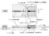
- FIG. 1 is a schematic diagram showing an optical integrated device structure in which a reflection type optical waveguide device and a silicon fine wire waveguide of this embodiment are integrated.
- FIG. 1 shows a top view and a side view as seen from above.
- FIG. 2 is a schematic diagram showing a basic configuration of the reflective optical waveguide element of FIG.
- FIG. 2 shows a top view, a side view, and a sectional view as seen from above.
- the optical waveguide device of the present embodiment is basically an intersubband transition device having a reflective structure (R1), and can be called an intersubband transition switch waveguide 10.
- the intersubband transition switch waveguide 10 is connected to the silicon fine wire waveguide 3 at the end face (P1) of the optical waveguide.
- the silicon thin wire waveguide 3 is formed on the silicon substrate 1 in the order of the SiO 2 lower cladding layer 2 and the SiO 2 upper cladding layer 4.
- the silicon thin wire waveguide 3 is a thin wire of about 200 nm, for example, and has a small mode cross-sectional area.
- the optical waveguide of the present invention has a multiple quantum well (MQW) composed of InGaAs / AlAsSb coupled quantum wells as a core layer, and a cladding layer such as an InAlAs layer is provided above and below the core layer. Phase modulation effects are produced by intersubband transitions.
- the intersubband transition switch waveguide 10 includes a substrate 11, multiple quantum wells (MQWs) having a coupled quantum well structure, cores 12 to 16, and a cladding layer 17.
- MQWs multiple quantum wells
- the coupled quantum well structure cores 12 to 16 use periodic layers of InGaAs / AlAsSb.
- the cladding layer 17 uses InAlAs.
- the optical waveguide has a structure capable of enhancing optical confinement such as a mesa-type waveguide as shown in the cross-sectional view of FIG. 2 by etching.
- the width of the MQW core layer that is the main part of the waveguide in the intersubband transition switch waveguide 10 is, for example, about 2 ⁇ m.
- the intersubband transition switch waveguide 10 has a waveguide end face (P1) and a waveguide end face (P2), and a reflection structure in which an optical signal incident from one of the waveguides is formed on the other end side.
- a structure reflecting (R1) is provided.
- a Bragg reflector having a periodic structure of semiconductor and air or a Bragg reflector having a periodic structure of SiO 2 and Si is formed to reflect the TE signal light.
- Structure (R1) is formed.
- the reflection structure (R1) is schematically illustrated in the top view and the side view of FIG. The reflectivity with respect to the TE signal light in the reflective structure (R1) affects the SN ratio, and is preferably as high as possible.
- the intersubband transition switch waveguide 10 is provided on the silicon substrate on which the silicon fine wire waveguide 3 is formed so as to be connected to the silicon fine wire waveguide. As shown in FIG. 1, the gap 6 having an appropriate gap length is provided, and the silicon fine wire waveguide 3 and the intersubband transition switch waveguide 10 are integrated to form an optical integrated device.
- an antireflection film 20 such as SiON or ZrO 2 on the end face (P1) of the optical waveguide.
- an intermediate layer having a different refractive index, such as the antireflection film 20 By inserting an intermediate layer having a different refractive index, such as the antireflection film 20, the reflection of the optical signal due to the difference in effective refractive index between the intersubband transition switch waveguide 10 and the silicon wire waveguide 3 is reduced, and Michelson The coupling efficiency with the interferometer can be improved.
- phase modulation region 30 the region from the waveguide end face (P1) to the reflection structure (R1) is a region where the signal light is subjected to the phase modulation effect (referred to as phase modulation region 30).
- the signal light 5 incident from the end face (P1) of the optical waveguide is subjected to the phase modulation effect until it travels to the reflection structure (R1), and the optical signal reflected by the reflection structure (R1)
- a length that allows the phase modulation region 30 to undergo the phase modulation again before returning to the waveguide end face (P1) is desirable.
- the relaxation time (about 2 ps) of the phase modulation effect and the group velocity of the optical signal about 10 to 300 ⁇ m is desirable.
- the TM control light can be introduced into the waveguide through the waveguide end face (P1) or the waveguide end face (P2).
- FIG. 3 is a cross-sectional view of a semiconductor crystal structure in which an InGaAs / AlAsSb coupled quantum well and a clad grown for use in manufacturing an optical waveguide of the present invention are grown.
- the semiconductor substrate 11 is semi-insulating InP, and each layer is grown on an AlAsSb buffer layer 12 formed on the substrate 11.
- the quantum well layers 15a and 15b constituting the coupled quantum well structure are n-type In 0.53 Ga 0.47 As having a carrier concentration of about 1 ⁇ 10 19 cm ⁇ 3 , and the well width ranges from 2.0 nm to 3 nm. 0.0 nm.
- the coupling barrier layer 16 between the quantum well layers 15a and 15b is non-dope InAlAs or AlGaAs, and its width is about 1.1 nm.
- the outer barrier layers 13a and 13b are non-doped AlAsSb and have a width of about 2.0 nm.
- An AlAs layer 14 is formed as an intermediate layer between the external barrier layer and the quantum well layer in order to prevent diffusion of carriers from the quantum well layer. After such a coupled quantum well layer is laminated for 40 to 70 periods, a non-doped InAlAs layer 17 (upper cladding) is formed.
- a semiconductor crystal layer including such a coupled quantum well structure can be formed by continuous growth on an InP substrate (lower cladding layer) by a growth method such as MBE or MOCVD.
- Subband excitation is performed by TM-polarized control light in the 1.55 ⁇ m band of the optical communication wavelength, and the TE-polarized signal light in the 1.55 ⁇ m band can be phase-modulated by the change in the refractive index due to the refractive index dispersion resulting therefrom.
- the film thickness is as follows.
- a mesa-type waveguide is manufactured by using a microfabrication technique by electron beam drawing or dry etching for the semiconductor crystal structure in which the InGaAs / AlAsSb coupled quantum well and the cladding shown in FIG. 3 are grown.
- a resist film is formed on the substrate having the semiconductor crystal growth structure, and a waveguide pattern is formed using electron beam drawing or the like.
- a metal mask of the waveguide pattern is produced by a transfer process using lift-off.
- a mesa waveguide is produced by dry etching using an ICP-RIE apparatus.
- the reflection structure of the waveguide can be manufactured by preparing a periodic structure having a different refractive index in the waveguide and utilizing Bragg reflection.
- the first method is a method in which an air layer is formed in a waveguide by dry etching and a difference in refractive index between the semiconductor layer and the air layer is used.
- the second method is a method in which a different material is periodically formed by sputtering or the like and a difference in refractive index between different materials is used.
- a well-known technique is employable.
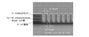
- FIG. 4 is an SEM photograph in the case where a reflective structure is actually produced in the waveguide by dry etching.
- a Bragg reflector having a period of 1.34 ⁇ m (semiconductor layer 0.6 ⁇ m, air layer 0.74 ⁇ m) is formed in the same optical waveguide as described in FIG.
- the reflection structure of FIG. 4 can be manufactured by adding a periodic structure pattern with a period of 1.34 ⁇ m when forming a pattern by EB drawing in the process for manufacturing a mesa waveguide described above.
- the optical waveguide includes an InP substrate 11, InGaAs / AlAsSb MQW core layers 12 to 16, and an InAlAs clad 17, and the air layer reaches the substrate.
- a waveguide having such an air layer reflection structure is advantageous in terms of reduction in the number of process steps, but it requires advanced technology because it is necessary to produce a submicron periodic structure by etching. .
- FIG. 5 is a schematic diagram in the case where a reflective structure is produced using a sputtering method.
- the reflection structure of FIG. 5 is formed by alternately forming materials having different refractive indexes, such as SiO 2 and Si, on the end face (P3) formed by dry etching or the like after a mesa waveguide is manufactured. Fabricate the film.
- the refractive index of each material is SiO 2 (refractive index 1.4) and Si (refractive index 3.5), and a Bragg reflector can be created from the refractive index difference between the two materials.
- CaF 2 (refractive index 1.43), LiF (refractive index 1.39), MgF 2 (refractive index 1.38), can be used, in place of Si, TiO 2 (Refractive index 2.5), CeO 2 (refractive index 2.40), CdS (refractive index 2.37), ZnS (refractive index 2.31), a-Si amorphous silicon (refractive index 3.6) are used. You can also. By producing a periodic structure of about 1 to 5 periods, a reflectance of 90% or more can be realized.
- the second method it is conceivable to form a film on the end face of the mirror-like waveguide formed by cleaving by sputtering, but the length of 10 to 300 ⁇ m assumed as the phase modulation region 30 is obtained by cleaving. Since this is difficult, an advanced technique for forming a good end face by dry etching or the like is required.
- a Si film or the like adheres to the side surface of the waveguide, it may cause a decrease in the waveguide characteristics. To prevent this, a low refractive index film such as SiN is used to prevent this. Waveguide protection should be performed.
- the reflection using the Bragg reflector has been described.
- a substance having a refractive index different from the effective refractive index of the waveguide on the waveguide end face (P2) the difference in refractive index between the two. Reflection by may be used.
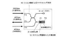
- FIG. 6 is a diagram showing coupling between an intersubband transition switch waveguide (reflection type waveguide) having a reflection structure and a Michelson interferometer according to the embodiment of the present invention.
- a Michelson interferometer instead of the Mach-Zehnder interferometer of FIG. 8 described in the prior art.
- a 160 Gbps TE signal light is input from the end face P1 of the intersubband transition switch waveguide via the first silicon fine wire waveguide 61a, and a 40 Gbps TM control light is supplied to the second silicon fine wire waveguide 61b.
- TM control light is supplied to the second silicon fine wire waveguide 61b.
- the end face P1 of the intersubband transition switch waveguide After the signal light phase-modulated in the waveguide by the TM control light is reflected by the reflection structure (R1), the interference light is generated by the light output from the waveguide end face P1 and reflected by the loop mirror 62.
- the optical gate switch can be realized by changing the phase difference between when the TM pump light is incident and when the TM pump light is not incident, thereby causing positive and negative interference.
- the TE signal light (160 Gbps) can be demultiplexed using the TM control light (40 Gbps), and the demultiplexed TE signal light (40 Gbps) is output from the third silicon wire waveguide 61c. be able to.
- the silicon fine wire waveguide only needs to be connected at one place on the waveguide end face (P1) of the intersubband transition switch waveguide. Increased efficiency can be expected. Further, by providing a reflecting structure, a phase modulation effect of about twice can be used. As a result, the effect of improving the performance of the switch, such as improving the SN ratio and reducing the input power, can be obtained.
- An antireflection layer 20 is provided on the waveguide end face (P1) of the intersubband transition switch waveguide of FIG.
- the antireflection layer 20 is made of a material having a different refractive index such as SiO 2 , TiO 2 , SiON, or ZrO 2 by a sputtering film forming method or the like.
- FIG. 7 shows the result of calculation of the coupling efficiency when the reflective waveguide shown in FIG. 1 and the silicon fine wire waveguide are connected using the time domain difference method (FDTD method).
- the horizontal axis represents a gap (unit: ⁇ m), and the vertical axis represents coupling efficiency.
- the reflection type waveguide has a waveguide width of 2 ⁇ m, a mesa height of 1.8 ⁇ m, and a phase modulation region of 50 ⁇ m.
- an SiON film was assumed on the waveguide end face (P1) as an antireflection film on the waveguide end face of the input / output signal.
- the silicon wire waveguide end is a spot size converter (waveguide width 200 nm, height 200 nm).
- the coupling efficiency is about 0.8 when there is no gap (0 ⁇ m), and the coupling efficiency is 0.63, 0.48, 0 when the gap is 0.5 ⁇ m, 1 ⁇ m, and 1.5 ⁇ m, respectively. .40.
- high coupling efficiency of 50% or more can be obtained by bringing the silicon fine wire waveguide and the intersubband transition switch waveguide end face (P1) close to about 1 ⁇ m.
- the intersubband transition element has been described as an example, but the same effect can be expected in the hybrid integration of the optical waveguide using the phase modulation effect.
- a fine wire waveguide using SiO 2 or a compound semiconductor may be used. The examples shown in the above embodiment are described for easy understanding of the invention, and are not limited to this embodiment.
Landscapes
- Physics & Mathematics (AREA)
- Nonlinear Science (AREA)
- Optics & Photonics (AREA)
- Chemical & Material Sciences (AREA)
- Engineering & Computer Science (AREA)
- Nanotechnology (AREA)
- General Physics & Mathematics (AREA)
- Life Sciences & Earth Sciences (AREA)
- Biophysics (AREA)
- Crystallography & Structural Chemistry (AREA)
- Optical Integrated Circuits (AREA)
- Optical Modulation, Optical Deflection, Nonlinear Optics, Optical Demodulation, Optical Logic Elements (AREA)
Abstract
サブバンド間遷移素子とシリコン細線によるハイブリット集積化において、シリコン細線との結合効率の向上、及び光路長増大による位相変調効果の増大を実現させ、光ゲートスイッチのSN比改善と低エネルギー動作化等の高性能化を実現する。InGaAsやAlAsSbなどの量子井戸構造を形成可能な半導体材料を用い、その量子井戸構造でのサブバンド間遷移によって引き起こされる位相変調効果を有するサブバンド間遷移導波路に、TE光信号に対する反射構造(R1)を設けてサブバンド間遷移スイッチ導波路10を構成する。導波路端面(P1)から入力された信号光5は、導波路で位相変調効果を受け、光導波路に設けた反射構造(R1)にて反射され、再び、導波路内で位相変調効果を受けて、導波路端面(P1)から出力されるので、シリコン細線導波路との入出力端の同一化および光路長増大を実現できる。
Description
本発明は、位相変調効果を持つ光導波路素子、該光導波路素子を用いた光集積回路、光ゲートスイッチ、及び前記光導波路素子の製造方法に関する。
近年の情報通信技術の飛躍的進歩により、インターネットトラフィックは年率40%の増加を示している。これに伴った、ルーターをはじめとした光通信用伝送装置での消費電力増大が懸念されている。現在の光通信ネットワークでは、大容量の光信号を伝送する場合、光信号を圧縮させて伝送している。このような圧縮処理がルーターなどの光信号伝送装置での消費電力増大に繋がっている。この対策として、できるだけ大容量光信号を非圧縮に伝送することで、高効率なネットワーク実現することが期待されている。今後増加していくと予想される高精細画像などの大容量伝送をローカルネットワークなどへ導入していくことで、将来の光通信ネットワークの低エネルギー化への貢献が期待されている。
このためには、大容量光信号を低電力で送受信可能な、光ネットワークインターフェースカード(光NIC)が不可欠となる(非特許文献1参照)。現在製品化されている光NICは、光ゲートスイッチに電気的処理を用いているため、送受信速度は40Gbpsと遅く、今後も送受信速度の飛躍的な向上は望めない。一方、光NICに用いられる光ゲートスイッチとして、InGaAs/AlAsSb量子井戸でのサブバンド間遷移現象を利用した全光型ゲートスイッチがあり、160Gbps以上で動作可能な光NICの実現が期待できる(特許文献1参照)。
サブバンド間遷移素子では、TMポンプ光(制御光)によって、量子井戸の電子がサブバンド間励起されると、屈折率分散によってTE信号の位相が変調される(位相変調効果)。このため、マッハツェンダー干渉計の片方アームにサブバンド間遷移素子を挿入すると、TMポンプ光の入射時と非入射時で、両アームでの位相差が変わるため、光ゲートスイッチを実現することができる(非特許文献2参照)。これまで、InGaAs/AlAsSb量子井戸からなるサブバンド間遷移素子で引き起こされる位相変調効果を用いて、空間型マッハツェンダー干渉計にて、全光型ゲートスイッチの動作実験を行い、4pJの入力エネルギーで160Gbpsから40Gbpsへの多重分離動作などの全光型ゲート動作が可能であることを発明者らは確認している(非特許文献3参照)。
光NICを社会的に普及していくには、出来る限りの低コスト化、小型化及び低エネルギー動作化が望ましい。全光型ゲート動作を実験的に既に確認している空間型のマッハツェンダー干渉計では、このような要求を満足できない。シリコン基板などのプラットフォーム上に、シリコン細線導波路等を用いて、マッハツェンダー干渉計などを構成する方が望ましい。このような背景から、これまで、シリコン細線導波路とサブバンド間遷移素子を用いたハイブリット集積型光NICが提案されている(非特許文献1参照)。
また、本発明について関連する文献として、非特許文献4乃至6がある。シリコン細線導波路とサブバンド間遷移素子を用いたハイブリット集積型光NICを実現するには、高度な半導体微細加工技術が必要となる。スパッタ法による多層膜反射鏡の作製、及び、蒸着法による金属膜反射鏡の作製などの従来技術に加えて(非特許文献4参照)、近年、ドライエッチング技術を用いたブラック反射鏡の作製(非特許文献5参照)、シリコン細線導波路によるマイケルソン干渉計の作製(非特許文献6参照)などが報告され、ハイブリット集積型光NIC実現のための有効な技術要素が整ってきている。
石川浩,「低消費電力の超大容量ネットワークからの期待」,財団法人光産業技術振興協会平成20年度シリコンフォトニクスブレークスルー技術調査報告書(FY2008-001-3)、pp.45-58,2009年3月.
H.Tsuchida,T.Simoyama,H.Ishikawa,T.Mozume,M.Nagase,and J.Kasai,"Cross phase modulation-based wavelength conversion using intersubband transition in InGaAs/AlAs/AlAsSb coupled quantum wells",Opt.Lett.,vol.32,no.7,pp.751-753,2007.
R.Akimoto,G.W.Cong,M.Nagase,T.Mozume,H.Tsuchida,T.Hasama,and H.Ishikawa,"All-optical demultiplexing from 160 to 40/80 Gb/s Using Mach-Zehnder switches based on intersubband transition of InGaAs/AlAsSb coupled double quantum wells",IEICE Trans. Electron.,vol.E92-C,no.6,pp.187-193,2009.
伊賀健一、小山二三夫,"面発光レーザ"オーム社,chapter5,1990.
M.Madhan Raj,J.Wiedmann,S.Toyoshima,Y.Saka,K.Ebihara and S.Arai,"High-Reflectivity Semiconductor/Benzocyclobutene Bragg Reflector Mirrors for GaInAsP/InP Lasers",Jpn.J.Appl.Phys.vol.40,pp.2269-2277,2001
J.Song,Q.Fang,S.H.Tao,T.Y.Liow,M.B.Yu,G.Q.Lo and D.L.Kwong,"Fast and low power Michelson interferometer thermo-optical switch on SOI",Optics Express,vol.16,no.20,pp.15304-15311,2008.
ハイブリット集積型光NICにおいては、シリコン細線導波路およびサブバンド間遷移素子との結合効率が、光ゲートスイッチ性能に大きな影響をもたらす。結合効率が減少すると、実質的に位相変調効率を低下させるためTM制御光の入力パワー増加が必要となる。また、結合損失増大によるTE信号光減衰によって、SN比低下の問題が生じる。
従来の、ハイブリット集積型光NICを構成しているマッハツェンダー干渉計について図8を参照して説明する(非特許文献1参照)。図8は、従来型のサブバンド間遷移スイッチ導波路80とマッハツェンダー干渉計81との結合を示す図である。160GbpsのTE信号光を第1のシリコン細線導波路82aを介してサブバンド間遷移スイッチ導波路P1から入力すると共に、40GbpsのTM制御光を第2のシリコン細線導波路82bを介してサブバンド間遷移スイッチ導波路80に入力する。TM制御光により、サブバンド間遷移スイッチ導波路内で位相変調を起こすことで、マッハツェンダー干渉計の両アームでの信号光の位相差が変わり、82cでおこる信号光の干渉効果の正と負が逆転する。これより、TM制御光(40Gbps)と同じタイミングを持つTE信号光(40Gbps)のみをサブバンド間遷移スイッチ導波路端面82cから出力することができる。いわゆる160Gbpsから40Gbpsへの多重分離動作(DEMUX動作)を可能とする。
図8の場合、サブバンド間遷移スイッチ導波路80(メサ型導波路、導波路幅:約2μm、導波路高さ:約2μm、長さ:300μm)の入力側端面(P1)と出力側端面(P2)の2箇所で、シリコン細線導波路(導波路幅:200nm、導波路高さ:200nm)と接続する必要があり、高度な実装技術を必要とする。このように、従来のハイブリット集積型光NICのマッハツェンダー干渉計では、シリコン細線導波路とメサ型導波路を結合させる必要があるが、結合効率を50%以上とする位置合わせの許容度は、サブミクロンと非常に狭く、高度な実装技術が不可欠となるという問題がある。
また、サブバンド間遷移素子とシリコン細線導波路の集積化において、両者のわずかな位置ずれによって、結合効率が大きく低下する。これにより、実質的に位相変調効率が低下してしまうため、TM制御光の入力パワーを大きくする必要がある。また、結合効率の低下に伴う信号光の減衰により、SN比が低下するという問題がある。
本発明は、これらの問題を解決しようとするものであり、サブバンド間遷移素子等とシリコン細線等の結合効率を向上することを目的とし、さらにサブバンド間遷移素子等における位相変調効率を増大させることを目的とする。また、高性能な光ゲートスイッチを実現することを目的とする。
高度な位置合わせ精度の必要性は、モード断面積がそれぞれ小さいシリコン細線とサブバンド間遷移素子とを、光入力側端面(P1)と光出力側端面(P2)の2箇所で接続しなければならないことに起因している。
そこで、発明者らは、この問題を解決し、サブバンド間遷移素子をシリコン細線導波路に集積可能にするために、反射構造を持つ導波路をサブバンド間遷移素子に利用することを提案するものである。本発明の導波路素子では、導波路端面(P1)から入力された光信号は、導波路内で位相変調効果を受けて、導波路に設けた反射構造(R1)にて光信号が反射され、再び、導波路内で位相変調効果を受けて、導波路端面(P1)から出力される。これにより、入力側及び出力側の導波路が同一となり、シリコン細線導波路との接続点が1点に減少できることから、結合効率の改善が可能となる。また、導波路内で2回の位相変調効果を受けるため、約2倍の位相変調効率を得ることが可能になる。
本発明は、前記目的を達成するために、以下の特徴を有するものである。
本発明は、位相変調効果を有する光導波路素子であって、光導波路の導波路端面から入射した光信号に対する反射構造を備えることを特徴とする。本発明の光導波路素子において、前記光信号が前記反射構造で反射され前記導波路端面から出力されることにより、位相変調領域での光信号の光路長が増大される。前記光導波路は、量子井戸構造を形成する半導体材料からなり、前記量子井戸構造でのサブバンド間遷移によって引き起こされる位相変調効果を有する。例えば、前記光導波路は、InGaAsとAlAsSbからなる量子井戸構造を形成する半導体材料からなる。位相変調効果を有する光導波路素子として、サブバンド間遷移素子の他に、キャリアプラズマ効果、熱光学効果、Kerr効果、ポッケルス効果のいずれか1つ以上による位相変調を利用した素子を用いてもよい。前記反射構造は、代表的には、ブラッグ反射鏡の構造である。他に、金属膜反射鏡やファセットミラーも利用可能である。本発明の導波路素子において、光が入出力する前記導波路端面には、反射防止層を備えることが好ましい。
本発明では、シリコン細線導波路によるマイケルソン干渉計と光信号の入出力が可能である。本発明は、光集積回路であって、前記光導波路素子とシリコン細線導波路とを結合して光集積回路とすることができる。本発明は、光ゲートスイッチであり、前記光導波路素子とシリコン細線導波路によるマイケルソン干渉計とを結合して光ゲートスイッチとすることができる。
本発明の方法は、位相変調効果を有する光導波路素子の製造方法であって、光導波路の一方の導波路端面から入射した光信号に対する反射構造を、前記光導波路の他方の導波路端面側に形成することを特徴とする。また、光導波路の導波路端面から入射した光信号に対する反射構造を、前記光導波路に空気層の周期構造をエッチングして形成することを特徴とする。また、光導波路の一方の導波路端面から入射した光信号に対する反射構造を、前記光導波路の他方の導波路端面に屈折率の異なる材料を交互に成膜して形成することを特徴とする。成膜は、スパッタや蒸着により形成することが好ましい。
本発明では、導波路に反射構造を持つサブバンド間遷移素子を実現したことにより、サブバンド間遷移導波路とシリコン細線を用いたハイブリット集積化において、素子間結合効率を向上させ、及び位相変調効果の増大させることができる。その結果、さらに、光ゲートスイッチの高性能化を実現できる。また、本発明では、サブバンド間遷移素子とシリコン細線の位置合わせにおいて要求される精度が低くなるため、歩留まり向上を期待できる。
サブバンド間遷移素子の他、キャリアプラズマ効果、熱光学効果、Kerr効果、ポッケルス効果による位相変調を利用した素子も、位相変調効果を利用する光導波路のハイブリット集積化において、同様な効果を期待できる。
以下に、本発明を実施するための形態を説明する。本発明は、基本構造として、反射構造をサブバンド間遷移光導波路に設けるものである。本発明では、光導波路の端面である導波路端面(P1)又は導波路端面(P2)から入射されたTM制御光によって、TE信号光に対する位相変調が可能な光導波路に、TE光信号に対する反射構造(R1)を設け、また、導波路端面(P1)に反射防止層を設けている。反射構造(R1)によって、信号光を位相変調領域内で反射させることにより、光路長増大により位相変調効果が増大する。また、導波路端面(P1)に反射防止層を設けることにより、同一端面からの高効率な光入出力を実現できる。
(第1の実施の形態)
本発明の第1の実施の形態について、図1乃至7を参照して以下説明する。図1は、本実施の形態の反射型の光導波路素子とシリコン細線導波路を集積した光集積素子構造を示す模式図である。図1に、上から見た上面図と、側面図を示す。図2は、図1の反射型の光導波路素子の基本構成を示す模式図である。図2に、上から見た上面図と、側面図と、断面図とを示す。
本発明の第1の実施の形態について、図1乃至7を参照して以下説明する。図1は、本実施の形態の反射型の光導波路素子とシリコン細線導波路を集積した光集積素子構造を示す模式図である。図1に、上から見た上面図と、側面図を示す。図2は、図1の反射型の光導波路素子の基本構成を示す模式図である。図2に、上から見た上面図と、側面図と、断面図とを示す。
本実施の形態の光導波路素子は、基本的に反射構造(R1)を有するサブバンド間遷移素子であり、サブバンド間遷移スイッチ導波路10と呼ぶことができる。サブバンド間遷移スイッチ導波路10は、シリコン細線導波路3と、光導波路端面(P1)で接続される。シリコン細線導波路3は、シリコン基板1上に、SiO2下部クラッド層2、SiO2上部クラッド層4の順で形成されている。シリコン細線導波路3は、例えば200nm程度の細線でありモード断面積が小さい。
本発明の光導波路は、InGaAs/AlAsSb結合量子井戸により構成した多重量子井戸(MQW)をコア層とし、その上下部にInAlAs層などのクラッド層が設けてあり、InGaAs/AlAsSb結合量子井戸でのサブバンド間遷移によって位相変調効果を生じる。図1及び図2に示すように、サブバンド間遷移スイッチ導波路10は、基板11と、結合量子井戸構造からなる多重量子井戸(MQW)、コア12~16と、クラッド層17とを有する。基板11は、例えばInP基板を用いる。結合量子井戸構造コア12~16は、InGaAs/AlAsSbの周期層を用いる。クラッド層17は、InAlAsを用いる。
光導波路は、エッチング加工によって、図2の断面図に示すようにメサ型導波路などの光閉じ込め増強可能な構造となっている。サブバンド間遷移スイッチ導波路10における導波路主要部であるMQWコア層の幅は、例えば2μm程度である。
サブバンド間遷移スイッチ導波路10は、導波路端面(P1)と導波路端面(P2)を有し、いずれか一方の導波路から入射した光信号を、他端側に形成されている反射構造(R1)で反射する構造を備えている。サブバンド間遷移スイッチ導波路10の光導波路内に、半導体と空気による周期構造によるブラッグ反射鏡、あるいは、SiO2とSiなどの周期構造によるブラッグ反射鏡などを形成して、TE信号光に対する反射構造(R1)を形成する。図2の上面図及び側面図に、反射構造(R1)を模式的に図示した。反射構造(R1)でのTE信号光に対する反射率は、SN比に影響するため、できる限り高い方が望ましい。
サブバンド間遷移スイッチ導波路10は、シリコン細線導波路3の形成されたシリコン基板上にシリコン細線導波路に接続するように設けられている。図1に示すように、適切なギャップ長のギャップ6を設けてシリコン細線導波路3とサブバンド間遷移スイッチ導波路10が集積されて、光集積素子を形成している。
光導波路端面(P1)には、SiON、ZrO2などの反射防止膜20を設けることが好ましい。反射防止膜20のような屈折率の異なる中間層の挿入により、サブバンド間遷移スイッチ導波路10とシリコン細線導波路3との有効屈折率の違いによる光信号の反射を少なくして、マイケルソン干渉計との結合効率を向上させることができる。
図1に示されるように、導波路端面(P1)から入力された信号光5は、導波路で位相変調効果を受けて、光導波路に設けた反射構造(R1)にて、反射され、再び、導波路内で位相変調効果を受けて、導波路端面(P1)から出力される。導波路端面(P1)から反射構造(R1)までが、信号光が位相変調効果を受ける領域(位相変調領域30と呼ぶ)である。ここでは、光導波路端面(P1)から入射された信号光5が、反射構造(R1)まで進行するまでに位相変調効果を受け、さらに、反射構造(R1)で反射された光信号が、光導波路端面(P1)まで戻るまでに、位相変調領域30で再び位相変調を受けることができる長さが望ましい。また、位相変調効果の緩和時間(約2ps)と光信号の群速度との関係を考慮すると、10~300μm程度が望ましい。
導波路端面(P1)あるいは導波路端面(P2)を介して、TM制御光を導波路内へ導入可能であることが好ましい。
図3は、本発明の光導波路作製に用いられるInGaAs/AlAsSb結合量子井戸とクラッドを成長した半導体結晶構造の断面である。半導体基板11は半絶縁性InPであり、各層は基板11上にAlAsSbバッファ層12を形成した上に成長形成されている。結合量子井戸構造を構成する量子井戸層15a、15bは、キャリア濃度約1×1019cm-3のn型In0.53Ga0.47Asであり、その井戸幅は、2.0nmから3.0nmである。各量子井戸層15a及び15b間の結合障壁層16は、ノンドーブのInAlAs、または、AlGaAsであり、その幅は、約1.1nmである。外部障壁層13a、13bは、ノンドープのAlAsSbであり、その幅は、約2.0nmである。外部障壁層と量子井戸層の間には、量子井戸層からのキャリアの拡散を防ぐために、中間層として、AlAs層14が形成されている。このような結合量子井戸層が40~70周期積層された後、ノンドープのInAlAs層17(上部クラッド)が形成されている。このような結合量子井戸構造を含んだ半導体結晶層は、MBE法、MOCVD法などの成長法によって、InP基板(下部クラッド層)の上に連続成長によって形成することができる。光通信波長の1.55μm帯のTM偏光の制御光によってサブバンド励起がなされ、それに起因した屈折率分散による屈折率変化によって、1.55μm帯のTE偏光の信号光を位相変調することができるような膜厚になっている。
本実施の形態のサブバンド間遷移スイッチ導波路の作製方法について以下説明する。
まず、図3に示した、InGaAs/AlAsSb結合量子井戸とクラッドを成長した半導体結晶構造に対して、電子線描画やドライエッチングによる微細加工技術を用いて、メサ型導波路を作製する。具体的には、上記半導体結晶成長構造を有する基板に、レジスト膜を形成し、電子線描画等を用いて導波路パターンを形成する。導波路パターン形成後、リフトオフを用いた転写プロセスによって、導波路パターンの金属マスクを作製する。金属マスク形成後、ICP-RIE装置を用いたドライエッチングによって、メサ型導波路を作製する。
次に、導波路に設ける反射構造の作製方法について説明する。導波路の反射構造は、導波路内に屈折率の異なる周期構造を作製し、ブラッグ反射を利用することで作製できる。第1の方法は、ドライエッチングによって導波路に空気層を形成し半導体層と空気層などとの屈折率差を利用する方法である。第2の方法は、スパッタ法などによって異種材料の周期的に成膜し異種材料の屈折率差を利用する方法である。なお、ブラッグ反射鏡の構造及び製造法については、公知の技術を採用することができる。
第1の方法について図4を参照して説明する。図4は、実際に、ドライエッチングによって、導波路に反射構造を作製した場合のSEM写真である。図2で説明したと同様の光導波路に、周期1.34μm(半導体層0.6μm、空気層0.74μm)のブラッグ反射鏡が形成されている。図4の反射構造は、先に述べたメサ型導波路の作製プロセスでの、EB描画によるパターン形成の際に、周期1.34μmの周期構造パターンを追加することで作製できる。光導波路は、InP基板11と、InGaAs/AlAsSbのMQWコア層12~16と、InAlAsクラッド17からなり、空気層は、基板にまで達している。また、エッチングされた空気層には、導波路保護や放射損抑制のために、BCB(benzocyclobutene、ベンゾシクロブテン)やSiO2などの低屈折率材料を埋め込むことが好ましく、波長1.55μmに対して、90%以上の反射率を実現できる。このような空気層による反射構造を有する導波路は、プロセス工数の削減という点で有利となるが、サブミクロンの周期構造をエッチングにより作製することが必要となるため、高度な技術を必要とする。
第2の方法について図5を参照して説明する。図5は、スパッタ法を用いて反射構造を作製した場合の模式図である。図5の反射構造は、メサ型導波路を作製した後に、ドライエッチングなどによって形成された端面(P3)に、SiO2、Siなどの屈折率の異なる材料を、スパッタ装置を用いて交互に成膜して作製する。各材料の屈折率は、SiO2(屈折率1.4)、Si(屈折率3.5)であり、両者の屈折率差からブラッグ反射鏡を作成可能である。また、SiO2の代わりに、CaF2(屈折率1.43)、LiF(屈折率1.39)、MgF2(屈折率1.38)、を用いることができ、Siの代わりに、TiO2(屈折率2.5)、CeO2(屈折率2.40)、CdS(屈折率2.37)、ZnS(屈折率2.31)、a-Siアモルファスシリコン(屈折率3.6)を用いることもできる。1~5周期程度の周期構造を作製することによって、反射率90%以上を実現できる。第2の方法では、劈開によって形成された鏡面状の導波路端面にスパッタ法により成膜することも考えられるが、位相変調領域30として想定している、10~300μmの長さを劈開によって得ることは困難なため、ドライエッチングなどによって、良好な端面を形成する高度な技術を必要とする。また、導波路側面へSi膜などが付着した場合には、導波路特性低下の要因になるおそれがあるが、これを防ぐには、スパッタ成膜前に、SiNなどの低屈折率膜で導波路保護を行うとよい。
本実施の形態では、ブラッグ反射鏡を用いた反射について説明したが、導波路の有効屈折率と異なる屈折率を持つ物質を、導波路端面(P2)に配置することで、両者の屈折率差による反射を用いてもよい。
次に、サブバンド間遷移スイッチ導波路10とシリコン細線導波路3との接続について説明する。図6は、本発明の実施の形態に係わる、反射構造を有するサブバンド間遷移スイッチ導波路(反射型導波路)とマイケルソン干渉計との結合を示す図である。本発明のような信号光の反射を利用する場合、従来技術で説明した図8のマッハツェンダー干渉計の代わりに、マイケルソン干渉計を利用することが可能になる。
図6では、160GbpsのTE信号光を第1のシリコン細線導波路61aを介してサブバンド間遷移スイッチ導波路の端面P1から入力すると共に、40GbpsのTM制御光を第2のシリコン細線導波路61bを介してサブバンド間遷移スイッチ導波路の端面P1から入力する。TM制御光により導波路内で位相変調を受けた信号光が反射構造(R1)で反射された後に、導波路端面P1から出力され、一方ループミラー62で反射される光とによって干渉効果が起こる。TMポンプ光の入射時と非入射時で、位相差が変わり、正と負の干渉を起こすことによって、光ゲートスイッチを実現することができる。これより、TE信号光(160Gbps)をTM制御光(40Gbps)で多重分離動作することが可能になり、第3のシリコン細線導波路61cから、多重分離されたTE信号光(40Gbps)を出力することができる。
本発明の実施の形態の場合、図6のように、サブバンド間遷移スイッチ導波路の導波路端面(P1)の1箇所でのみ、シリコン細線導波路を接続すればよいので、素子間の結合効率の向上を期待できる。また、反射構造を設けることで、約2倍の位相変調効果を利用できる。これにより、SN比改善や入力パワー低減などのスイッチの高性能化という効果が得られる。
図6のサブバンド間遷移スイッチ導波路の導波路端面(P1)には、反射防止層20が設けられている。サブバンド間遷移スイッチ導波路10をシリコン細線導波路に実装したときに、導波路間の隙間にできた空気等とサブバンド間遷移スイッチ導波路の屈折率差による信号光の反射を防止するために有効である。反射防止層20は、SiO2、TiO2、SiON、ZrO2などの屈折率の異なる物質をスパッタ成膜法等により作製する。
図7は、図1に示した反射型導波路とシリコン細線導波路を接続した場合の結合効率を、時間領域差分法(FDTD法)を用いて計算した結果である。図7の横軸はギャップ(単位μm)、縦軸は、結合効率(Coupling efficiency)を示す。反射型導波路は、導波路幅を2μm、メサ高さを1.8μm、位相変調領域を50μmとしている。また、導波路端面(P1)には、入出力信号の導波路端面での反射防止膜として、SiON膜を仮定した。シリコン細線導波路端は、スポットサイズ変換器(導波路幅200nm、高さ200nm)となっている。図7には、ギャップがない(0μm)とき結合効率が約0.8であり、ギャップが0.5μm、1μm、1.5μmのとき、それぞれ結合効率は、0.63、0.48、0.40である。図7に示すように、シリコン細線導波路とサブバンド間遷移スイッチ導波路端面(P1)を1μm程度に近づけることで、50%以上の高い結合効率が得られることを確認している。
実施の形態では、サブバンド間遷移素子を例にとって説明したが、位相変調効果を利用する光導波路のハイブリット集積化において、同様な効果を期待できる。また、シリコン細線導波路による例に挙げたが、SiO2や化合物半導体を用いた細線導波路などを用いても良い。上記実施の形態で示した例は、発明を理解しやすくするために記載したものであり、この形態に限定されるものではない。
1 シリコン基板
2 SiO2下部クラッド
3 シリコン細線導波路
4 SiO2上部クラッド
5 信号光
6 ギャップ
10 サブバンド間遷移スイッチ導波路
11 InP基板(下部クラッド)
12 AlAsSbバッファ層
13(13a、13b) AlAsSb外部障壁層
14 AlAs拡散防止層
15(15a、15b) InGaAs量子井戸層
16 InAlAs結合障壁層
17 InAlAsキャップ層(上部クラッド)
20 反射防止膜
30 位相変調領域
40 多層膜反射鏡
41 SiO2
42 Si
60 シリコン細線によるマイケルソン干渉計
61(61a、61b、61c) シリコン細線導波路
62 ループミラー
80 サブバンド間遷移スイッチ導波路
81 シリコン細線によるマッハツェンダー干渉計
82(82a、82b、82c) シリコン細線導波路
2 SiO2下部クラッド
3 シリコン細線導波路
4 SiO2上部クラッド
5 信号光
6 ギャップ
10 サブバンド間遷移スイッチ導波路
11 InP基板(下部クラッド)
12 AlAsSbバッファ層
13(13a、13b) AlAsSb外部障壁層
14 AlAs拡散防止層
15(15a、15b) InGaAs量子井戸層
16 InAlAs結合障壁層
17 InAlAsキャップ層(上部クラッド)
20 反射防止膜
30 位相変調領域
40 多層膜反射鏡
41 SiO2
42 Si
60 シリコン細線によるマイケルソン干渉計
61(61a、61b、61c) シリコン細線導波路
62 ループミラー
80 サブバンド間遷移スイッチ導波路
81 シリコン細線によるマッハツェンダー干渉計
82(82a、82b、82c) シリコン細線導波路
Claims (12)
- 位相変調効果を有する光導波路素子であって、光導波路の導波路端面から入射した光信号に対する反射構造を備え、前記光信号が前記反射構造で反射され前記導波路端面から出力されることにより、位相変調領域での光信号の光路長が増大されることを特徴とする光導波路素子。
- 前記光導波路は、量子井戸構造を形成する半導体材料からなり、前記量子井戸構造でのサブバンド間遷移によって引き起こされる位相変調効果を有することを特徴とする請求項1に記載の光導波路素子。
- 前記光導波路は、InGaAsとAlAsSbからなる量子井戸構造を形成する半導体材料からなることを特徴とする請求項2記載の光導波路素子。
- キャリアプラズマ効果、熱光学効果、Kerr効果、ポッケルス効果のいずれか1つ以上による位相変調を利用したことを特徴とする請求項1記載の光導波路素子。
- 前記光導波路の前記反射構造は、ブラッグ反射鏡、金属膜反射鏡、ファセットミラーの少なくとも一つを用いた構造であることを特徴とする請求項1乃至4のいずれか1項に記載の光導波路素子。
- 前記導波路端面に反射防止層を備えることを特徴とする請求項1乃至5のいずれか1項に記載の光導波路素子。
- マイケルソン干渉計と光信号の入出力を可能とすることを特徴とする請求項1乃至6のいずれか1項に記載の光導波路素子。
- 請求項1乃至7のいずれか1項に記載の光導波路素子を結合したことを特徴とする光集積回路。
- 請求項1乃至7のいずれか1項に記載の光導波路素子と、シリコン細線導波路によるマイケルソン干渉計とを結合したことを特徴とする光ゲートスイッチ。
- 位相変調効果を有する光導波路素子の製造方法であって、
光導波路の一方の導波路端面から入射した光信号に対する反射構造を、前記光導波路の他方の導波路端面側に形成することを特徴とする請求項1記載の光導波路素子の製造方法。 - 位相変調効果を有する光導波路素子の製造方法であって、
光導波路の導波路端面から入射した光信号に対する反射構造を、前記光導波路に空気層の周期構造をエッチングして形成することを特徴とする請求項10記載の光導波路素子の製造方法。 - 位相変調効果を有する光導波路素子の製造方法であって、
光導波路の一方の導波路端面から入射した光信号に対する反射構造を、前記光導波路の他方の導波路端面に屈折率の異なる材料を交互に成膜して形成することを特徴とする請求項10記載の光導波路素子の製造方法。
Applications Claiming Priority (2)
| Application Number | Priority Date | Filing Date | Title |
|---|---|---|---|
| JP2010-145899 | 2010-06-28 | ||
| JP2010145899A JP5605621B2 (ja) | 2010-06-28 | 2010-06-28 | 光ゲートスイッチ |
Publications (1)
| Publication Number | Publication Date |
|---|---|
| WO2012002306A1 true WO2012002306A1 (ja) | 2012-01-05 |
Family
ID=45402019
Family Applications (1)
| Application Number | Title | Priority Date | Filing Date |
|---|---|---|---|
| PCT/JP2011/064635 Ceased WO2012002306A1 (ja) | 2010-06-28 | 2011-06-27 | 光導波路素子 |
Country Status (2)
| Country | Link |
|---|---|
| JP (1) | JP5605621B2 (ja) |
| WO (1) | WO2012002306A1 (ja) |
Families Citing this family (1)
| Publication number | Priority date | Publication date | Assignee | Title |
|---|---|---|---|---|
| CN103392149B (zh) | 2011-02-18 | 2016-04-06 | 独立行政法人产业技术综合研究所 | 光闸开关 |
Citations (2)
| Publication number | Priority date | Publication date | Assignee | Title |
|---|---|---|---|---|
| JPH10221725A (ja) * | 1997-02-12 | 1998-08-21 | Nippon Telegr & Teleph Corp <Ntt> | 波長変換回路 |
| JP2010054929A (ja) * | 2008-08-29 | 2010-03-11 | Toshiba Corp | 光結合デバイス |
-
2010
- 2010-06-28 JP JP2010145899A patent/JP5605621B2/ja not_active Expired - Fee Related
-
2011
- 2011-06-27 WO PCT/JP2011/064635 patent/WO2012002306A1/ja not_active Ceased
Patent Citations (2)
| Publication number | Priority date | Publication date | Assignee | Title |
|---|---|---|---|---|
| JPH10221725A (ja) * | 1997-02-12 | 1998-08-21 | Nippon Telegr & Teleph Corp <Ntt> | 波長変換回路 |
| JP2010054929A (ja) * | 2008-08-29 | 2010-03-11 | Toshiba Corp | 光結合デバイス |
Non-Patent Citations (3)
| Title |
|---|
| JOURNAL OF LIGHTWAVE TECHNOLOGY, vol. 26, no. 19, 1 October 2008 (2008-10-01), pages 3363 - 3368 * |
| OPTICS EXPRESS, vol. 16, no. 20, 29 September 2008 (2008-09-29), pages 15304 - 15311 * |
| RYOICHI AKIMOTO ET AL.: "All-optical phase modulation using intersubband transition in quantum wells", OYO BUTSURI, vol. 79, no. 3, 10 March 2010 (2010-03-10), pages 225 - 229 * |
Also Published As
| Publication number | Publication date |
|---|---|
| JP5605621B2 (ja) | 2014-10-15 |
| JP2012008430A (ja) | 2012-01-12 |
Similar Documents
| Publication | Publication Date | Title |
|---|---|---|
| JP5897414B2 (ja) | 光デバイスの製造方法 | |
| US9136672B2 (en) | Optical light source | |
| JP5573309B2 (ja) | マッハツェンダー型光変調素子 | |
| Sciancalepore et al. | CMOS-compatible ultra-compact 1.55-μ m emitting VCSELs using double photonic crystal mirrors | |
| US8472109B2 (en) | Semiconductor optical amplifier and optical module | |
| CN1272885C (zh) | 分布反馈半导体激光器与电吸收调制器集成光源及制法 | |
| CN103337788A (zh) | 基于重构—等效啁啾的非对称结构的dfb半导体激光器及制备 | |
| CN103346475B (zh) | 单片集成耦合腔窄线宽半导体激光器 | |
| CN103117510A (zh) | 一种混合硅基回音壁模式微腔激光器 | |
| CN112003125B (zh) | 一种采用表面高阶光栅的直接调制半导体激光器 | |
| Morthier et al. | InP microdisk lasers integrated on Si for optical interconnects | |
| CN106575855A (zh) | 一种垂直腔面发射激光器vcsel | |
| JP2003510855A (ja) | 複合型キャビティ反射変調レーザシステム | |
| US20130207140A1 (en) | Semiconductor Optical Element Semiconductor Optical Module and Manufacturing Method Thereof | |
| CN103605218B (zh) | 波导型电光调制器及其制作方法 | |
| CN103457156A (zh) | 应用于高速并行光传输的大耦合对准容差半导体激光芯片及其光电器件 | |
| CN107026391A (zh) | 多波长混合集成光发射阵列 | |
| CN102684072A (zh) | 混合集成激光器及其制备方法 | |
| JP5605621B2 (ja) | 光ゲートスイッチ | |
| CN118676737B (zh) | InAs量子点激光器及其制备方法 | |
| JP2004063972A (ja) | 半導体レーザおよびその製造方法 | |
| CN110176718A (zh) | 一种基于高阶横模波导输出的混合集成激光器芯片结构 | |
| CN1174469C (zh) | 偏振不灵敏半导体光学放大器的制备方法 | |
| JP2001308368A (ja) | 光共振器構造素子 | |
| JPH07176822A (ja) | 半導体光源及びその製造方法 |
Legal Events
| Date | Code | Title | Description |
|---|---|---|---|
| 121 | Ep: the epo has been informed by wipo that ep was designated in this application |
Ref document number: 11800770 Country of ref document: EP Kind code of ref document: A1 |
|
| NENP | Non-entry into the national phase |
Ref country code: DE |
|
| 122 | Ep: pct application non-entry in european phase |
Ref document number: 11800770 Country of ref document: EP Kind code of ref document: A1 |