WO2012002258A1 - 表示装置及びその制御方法、プログラム並びに記録媒体 - Google Patents
表示装置及びその制御方法、プログラム並びに記録媒体 Download PDFInfo
- Publication number
- WO2012002258A1 WO2012002258A1 PCT/JP2011/064473 JP2011064473W WO2012002258A1 WO 2012002258 A1 WO2012002258 A1 WO 2012002258A1 JP 2011064473 W JP2011064473 W JP 2011064473W WO 2012002258 A1 WO2012002258 A1 WO 2012002258A1
- Authority
- WO
- WIPO (PCT)
- Prior art keywords
- image data
- data
- display device
- frame
- text
- Prior art date
- Legal status (The legal status is an assumption and is not a legal conclusion. Google has not performed a legal analysis and makes no representation as to the accuracy of the status listed.)
- Ceased
Links
Images








Classifications
-
- G—PHYSICS
- G09—EDUCATION; CRYPTOGRAPHY; DISPLAY; ADVERTISING; SEALS
- G09G—ARRANGEMENTS OR CIRCUITS FOR CONTROL OF INDICATING DEVICES USING STATIC MEANS TO PRESENT VARIABLE INFORMATION
- G09G3/00—Control arrangements or circuits, of interest only in connection with visual indicators other than cathode-ray tubes
- G09G3/20—Control arrangements or circuits, of interest only in connection with visual indicators other than cathode-ray tubes for presentation of an assembly of a number of characters, e.g. a page, by composing the assembly by combination of individual elements arranged in a matrix no fixed position being assigned to or needed to be assigned to the individual characters or partial characters
- G09G3/22—Control arrangements or circuits, of interest only in connection with visual indicators other than cathode-ray tubes for presentation of an assembly of a number of characters, e.g. a page, by composing the assembly by combination of individual elements arranged in a matrix no fixed position being assigned to or needed to be assigned to the individual characters or partial characters using controlled light sources
- G09G3/30—Control arrangements or circuits, of interest only in connection with visual indicators other than cathode-ray tubes for presentation of an assembly of a number of characters, e.g. a page, by composing the assembly by combination of individual elements arranged in a matrix no fixed position being assigned to or needed to be assigned to the individual characters or partial characters using controlled light sources using electroluminescent panels
- G09G3/32—Control arrangements or circuits, of interest only in connection with visual indicators other than cathode-ray tubes for presentation of an assembly of a number of characters, e.g. a page, by composing the assembly by combination of individual elements arranged in a matrix no fixed position being assigned to or needed to be assigned to the individual characters or partial characters using controlled light sources using electroluminescent panels semiconductive, e.g. using light-emitting diodes [LED]
- G09G3/3208—Control arrangements or circuits, of interest only in connection with visual indicators other than cathode-ray tubes for presentation of an assembly of a number of characters, e.g. a page, by composing the assembly by combination of individual elements arranged in a matrix no fixed position being assigned to or needed to be assigned to the individual characters or partial characters using controlled light sources using electroluminescent panels semiconductive, e.g. using light-emitting diodes [LED] organic, e.g. using organic light-emitting diodes [OLED]
- G09G3/3225—Control arrangements or circuits, of interest only in connection with visual indicators other than cathode-ray tubes for presentation of an assembly of a number of characters, e.g. a page, by composing the assembly by combination of individual elements arranged in a matrix no fixed position being assigned to or needed to be assigned to the individual characters or partial characters using controlled light sources using electroluminescent panels semiconductive, e.g. using light-emitting diodes [LED] organic, e.g. using organic light-emitting diodes [OLED] using an active matrix
- G09G3/3233—Control arrangements or circuits, of interest only in connection with visual indicators other than cathode-ray tubes for presentation of an assembly of a number of characters, e.g. a page, by composing the assembly by combination of individual elements arranged in a matrix no fixed position being assigned to or needed to be assigned to the individual characters or partial characters using controlled light sources using electroluminescent panels semiconductive, e.g. using light-emitting diodes [LED] organic, e.g. using organic light-emitting diodes [OLED] using an active matrix with pixel circuitry controlling the current through the light-emitting element
-
- G—PHYSICS
- G09—EDUCATION; CRYPTOGRAPHY; DISPLAY; ADVERTISING; SEALS
- G09G—ARRANGEMENTS OR CIRCUITS FOR CONTROL OF INDICATING DEVICES USING STATIC MEANS TO PRESENT VARIABLE INFORMATION
- G09G3/00—Control arrangements or circuits, of interest only in connection with visual indicators other than cathode-ray tubes
- G09G3/20—Control arrangements or circuits, of interest only in connection with visual indicators other than cathode-ray tubes for presentation of an assembly of a number of characters, e.g. a page, by composing the assembly by combination of individual elements arranged in a matrix no fixed position being assigned to or needed to be assigned to the individual characters or partial characters
- G09G3/2007—Display of intermediate tones
-
- G—PHYSICS
- G09—EDUCATION; CRYPTOGRAPHY; DISPLAY; ADVERTISING; SEALS
- G09G—ARRANGEMENTS OR CIRCUITS FOR CONTROL OF INDICATING DEVICES USING STATIC MEANS TO PRESENT VARIABLE INFORMATION
- G09G3/00—Control arrangements or circuits, of interest only in connection with visual indicators other than cathode-ray tubes
- G09G3/20—Control arrangements or circuits, of interest only in connection with visual indicators other than cathode-ray tubes for presentation of an assembly of a number of characters, e.g. a page, by composing the assembly by combination of individual elements arranged in a matrix no fixed position being assigned to or needed to be assigned to the individual characters or partial characters
- G09G3/34—Control arrangements or circuits, of interest only in connection with visual indicators other than cathode-ray tubes for presentation of an assembly of a number of characters, e.g. a page, by composing the assembly by combination of individual elements arranged in a matrix no fixed position being assigned to or needed to be assigned to the individual characters or partial characters by control of light from an independent source
- G09G3/36—Control arrangements or circuits, of interest only in connection with visual indicators other than cathode-ray tubes for presentation of an assembly of a number of characters, e.g. a page, by composing the assembly by combination of individual elements arranged in a matrix no fixed position being assigned to or needed to be assigned to the individual characters or partial characters by control of light from an independent source using liquid crystals
- G09G3/3611—Control of matrices with row and column drivers
- G09G3/3648—Control of matrices with row and column drivers using an active matrix
-
- G—PHYSICS
- G09—EDUCATION; CRYPTOGRAPHY; DISPLAY; ADVERTISING; SEALS
- G09G—ARRANGEMENTS OR CIRCUITS FOR CONTROL OF INDICATING DEVICES USING STATIC MEANS TO PRESENT VARIABLE INFORMATION
- G09G2330/00—Aspects of power supply; Aspects of display protection and defect management
- G09G2330/02—Details of power systems and of start or stop of display operation
- G09G2330/021—Power management, e.g. power saving
-
- G—PHYSICS
- G09—EDUCATION; CRYPTOGRAPHY; DISPLAY; ADVERTISING; SEALS
- G09G—ARRANGEMENTS OR CIRCUITS FOR CONTROL OF INDICATING DEVICES USING STATIC MEANS TO PRESENT VARIABLE INFORMATION
- G09G2340/00—Aspects of display data processing
- G09G2340/04—Changes in size, position or resolution of an image
- G09G2340/0407—Resolution change, inclusive of the use of different resolutions for different screen areas
- G09G2340/0435—Change or adaptation of the frame rate of the video stream
Definitions
- the present invention relates to a display device, a control method thereof, a program, and a recording medium.
- a reflective liquid crystal panel is often used because of low power consumption.
- a transmissive liquid crystal panel that can display more vividly, and a reduction in power consumption of the transmissive liquid crystal panel is desired.
- Patent Documents 1 and 2 describe reducing power consumption by paying attention to the rewriting of data.
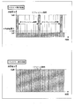
- FIG. 18A the display screen is divided into a display area and a non-display area, and partial driving is performed.
- FIG. 18 is a diagram for explaining a drive control method in a conventional display device. In this driving method, the frame is rewritten every frame in the display area, but the data is rewritten every several frames in the non-display area (see FIG. 18B).
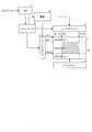
- FIG. 19 is a diagram illustrating a circuit configuration of a display panel included in a conventional display device.
- Japanese Patent Publication Japanese Patent Laid-Open No. 2003-58130 (published on February 28, 2003)” Japanese Patent Publication “Japanese Patent Laid-Open No. 9-331490 (published on December 22, 1997)”
- the aperture ratio decreases because the memory is built in the pixel. As a result, the area of the opening is reduced and the entire screen appears dark.
- the present invention has been made in view of the above problems, and an object thereof is to provide a display device capable of realizing low power consumption.
- a display device includes a display panel in which a plurality of scanning lines and a plurality of signal lines are arranged to cross each other, and each of the plurality of signal lines.
- a signal driver that supplies image data to be displayed on the display panel, input signal including the image data, and the signal line that supplies first image data included in the acquired input data are Control means for controlling the signal driver to supply the first image data at a lower frame frequency than the signal line for supplying the second image data included in the input data, and the control means comprises: A part of the input data is the first image data, and the rest is the second image data.
- a control method includes a display panel in which a plurality of scanning lines and a plurality of signal lines are arranged to intersect each other, and each of the plurality of signal lines.
- a control method for a display device comprising a signal driver for supplying image data for display on the display panel, the method comprising: obtaining input data including the image data; and first image data included in the acquired input data Control for controlling the signal driver to supply the first image data to the signal line for supplying the first image data at a lower frame frequency than the signal line for supplying the second image data included in the input data.
- a part of the input data is the first image data, and the remaining part is the second image data.
- the display device when input data including image data to be displayed on the display panel is acquired, among the acquired input data, a plurality of first image data and second image data are used.
- the frame frequency for supplying image data to each of the signal lines is changed.
- image data is supplied to the signal line that supplies the first image data at a lower frame frequency than the signal line that supplies the second image data.
- the polarity is generally inverted when writing a data signal, and power is consumed in this polarity inversion.
- the polarity inversion by the first image data is performed in order to make the frequency lower than the frame frequency at which the second image data is supplied to the signal line. The number decreases.
- the driving power of the signal driver that supplies the first pixel data to the signal line can be suppressed. Therefore, low power consumption can be realized.
- a display device includes a display panel in which a plurality of scanning lines and a plurality of signal lines are arranged to intersect with each other, and a display panel for displaying on each of the plurality of signal lines.
- a signal driver for supplying image data, and input signal including the image data are acquired, and the signal line for supplying the first image data included in the acquired input data is provided with a second signal included in the input data.
- FIG. 1 It is a block diagram which shows schematic structure of the principal part of the display apparatus which concerns on one Embodiment of this invention. It is a figure which shows the structure of the display panel with which the display apparatus shown in FIG. 1 is provided. 3 is a table showing a comparison of frame frequencies of a text display area and a full color display area in the display device shown in FIG. 1. It is a graph which shows the relationship between the oscillation frequency of a clock generator, and power consumption. It is a figure which shows the ratio of a full color display area and a text display area with respect to the whole screen of the display panel with which the display apparatus shown in FIG. 1 is provided.
- FIG. 1 It is a figure which shows the retention rate of the pixel potential of a text display area, and the retention rate of the pixel potential of a full color display area. It is a figure which shows the average power consumption concerning the data rewriting of the display panel with which the display apparatus shown in FIG. 1 is provided. It is a figure which shows the average power consumption concerning the data rewriting of each of a text display area and a full color display area.
- 3 is a table showing a comparison of frame frequencies of a text display area and a full color display area in the display device shown in FIG. 1. It is a figure which shows the ratio of a full color display area and a text display area with respect to the whole screen of the display panel with which the display apparatus shown in FIG. 1 is provided.
- FIG. 12 is a diagram illustrating an example of a flow of processing for converting multi-gradation data into 1-bit data in the display device illustrated in FIG. 11.
- 3 is a table showing a comparison of frame frequencies of a text display area and a full color display area in the display device shown in FIG. 1. It is a figure which shows the structure of the equivalent circuit of the display panel with which the display apparatus which concerns on other embodiment of this invention is provided. It is a table
- FIG. 1 is a block diagram showing a schematic configuration of a main part of a display device 100 according to an embodiment of the present invention.
- the display device 100 includes a liquid crystal panel 1 (display panel), a gate driver 2, a source driver 3 (signal driver), a power supply 4, a controller 5 (control means), and a backlight 6.
- the liquid crystal panel 1 is an active matrix type liquid crystal panel in which a plurality of pixels are arranged in a matrix. Although not shown, the liquid crystal panel 1 has a structure in which a liquid crystal layer is sandwiched between an active matrix substrate and a counter substrate.
- the liquid crystal panel 1 is not particularly limited as long as it is a transmissive liquid crystal panel, and a known liquid crystal panel can be used.
- FIG. 2 is a diagram illustrating a configuration of the liquid crystal panel 1 included in the display device 100.
- the gate line GL is connected to the gate driver 2, and the source line SL is connected to the source driver 3.
- a gate line GL, a source line SL, and a display electrode 12 are connected to the gate electrode, the source electrode, and the drain electrode of the switching element 13, respectively.
- the source signal is selectively supplied from the source driver 3 to the switching element 13 via the source line SL, and the gate signal is supplied from the gate driver 2 to the switching element 13 via the gate line GL. Control ON / OFF of.
- the gate driver 2 supplies a voltage as a gate signal to each gate line GL in the scanning order based on the gate control signal supplied from the controller 5.
- the source driver 3 supplies a source signal to each source line SL based on the source control signal supplied from the controller 5. Specifically, image data to be displayed on the liquid crystal panel 1 is supplied to each of the plurality of source lines SL.
- the power supply 4 applies a voltage necessary for supplying to the switching element 13 to the gate driver 2 and the source driver 3 based on a control signal supplied from the controller 5.
- the controller 5 acquires input data from an input data supply source (not shown), generates a gate control signal and a source control signal from the input data, supplies the generated gate control signal to the gate driver 2, and supplies the source control signal to the source This is supplied to the driver 3.
- the controller 5 acquires input data including image data, and the second image data included in the input data is supplied to the source line SL that supplies the first image data included in the acquired input data.
- the source driver 3 is controlled to supply the first image data at a frame frequency lower than that of the source line SL to be supplied.
- the controller 5 sets a part of the input data as the first image data and the rest as the second image data.
- the conditions at this time are not particularly limited.
- 1-bit to 4-bit image data may be used as the first image data for each of the three sub-pixels constituting the pixel.
- the first image data is 1-bit data.
- Other image data, that is, image data other than 1-bit to 4-bit image data for each sub-pixel is set as second image data.
- 1-bit image data is “FF” or “00” data
- binary 8 colors are displayed.
- FF FF
- 00 a monochrome image is displayed because the signal is displayed in either white or black.
- the voltage drop in one frame is about 7% of the voltage difference for each gradation when it is 4 bits (16 gradations). Even if the frame rate, which is normally 60 Hz, is set to 20 Hz (write once every three times), the amount of voltage change is about 20%, which is a level that is not problematic for text display.
- the 1-bit to 4-bit data includes, for example, text data and image data displayed by at least one color selected from the group consisting of white, black, and RGB primary colors.
- image data include books (characters, text), word processor documents, icons, and the like.
- the image data other than 1-bit to 4-bit data is an image displayed by a large number of gradations, that is, multi-bit image data having a large number of colors, for example, data of 5 bits or more.
- What is displayed by the second image data includes, for example, still images or moving images such as photographs or slide shows.
- an area for displaying the first image data is referred to as a text display area
- an area for displaying the second image data is referred to as a full color display area.
- a region 21 surrounded by a range from the source line SL1 to the source line SLn and a range from the gate line GL1 to the gate line GLn is a text display region.
- a region 20 surrounded by a range from the source line SLn to the source line SLn + a and a range from the gate line GLn to the gate line GLn + a is a full color display region.
- the area for displaying the first image data is referred to as a text display area.
- low-bit image data such as an icon included in the first image data is also displayed in text. Can be displayed in the area.
- the input data supply source is not particularly limited, and examples thereof include a mobile phone, a portable game machine, a PDA (Personal Digital Assistant), a digital camera, a notebook computer, and an electronic book.
- the backlight 6 is provided on the back side of the liquid crystal panel 1 (that is, the side opposite to the display surface) and irradiates the liquid crystal panel 1 with light.
- the backlight 6 is not particularly limited.
- a light source using a conventionally known light emitting element such as an LED (light emitting diode) may be used.
- the display device 100 includes the controller 5, but the controller 5 may be provided outside the display device 100. Further, although the gate driver 2 and the source driver 3 are provided outside the liquid crystal panel 1, at least one of the gate driver 2 and the source driver 3 may be formed integrally with the liquid crystal panel 1.
- the input data input from the input data supply source to the controller 5 includes image data such as text data, and control signals such as a horizontal synchronizing signal and a vertical synchronizing signal.
- the controller 5 acquires a control signal such as a horizontal synchronization signal and a vertical synchronization signal from an input data supply source, generates a gate control signal and a source control signal based on the acquired control signal, and generates a gate driver 2 and a source driver 3. To supply each.
- This gate control signal is a timing signal for controlling the driving timing of the gate driver 2, and includes a gate start pulse, a gate shift clock, a gate output enable, and the like.
- the data control signal is a timing signal for controlling the driving timing of the source driver 3, and includes a source start pulse, a source shift clock, a source output enable, a polarity inversion signal, and the like.
- the controller 5 acquires input data including image data to be displayed on the liquid crystal panel 1, among the acquired input data, the first image data and the second image data are: The frame frequency for supplying image data to each of the plurality of source lines SL is changed.
- the acquired input data is low-bit data of about 1 to 4 bits for each of the three sub-pixels constituting the pixel
- the first image data and the data with more bits are used. If so, the source line SL that determines the second image data and supplies the data determined as the first image data has a lower frame frequency than the source line SL that supplies the data determined as the second image data. Supply.
- low-bit image data of about 1 to 4 bits has a small number of gradation displays, so that the quality degradation of the image quality is less than that of data displaying multiple gradations. Therefore, even when low-bit image data is written at a low frame frequency, display quality is not impaired.
- the polarity is generally inverted when writing a data signal, but power is consumed in this polarity inversion.
- the first image data since the first image data has little deterioration in the quality of the image quality, it can be made lower than the frame frequency at which the second image data is supplied to the source line SL. Therefore, the number of polarity inversions by the first image data is reduced, and the driving power of the source driver 3 that supplies the first pixel data to the source line SL can be suppressed. Therefore, low power consumption can be realized.
- the frame frequency represents the number of frames rewritten per second.
- the normal frame frequency that is, the state in which the frame frequency is not lowered
- frame rewriting is also referred to as “writing” or “refreshing”.
- FIG. 3 shows a comparison of frame frequencies between the text display area and the full color display area in the present embodiment.
- FIG. 3 is a table showing a comparison of frame frequencies in the text display area and the full-color display area in the display device 100.
- every frame is rewritten in the full color display area.
- rewriting is performed in the first frame 1, but frames 2 to 10 are standby frames (pause frames) and are not rewritten.
- the period of the frame in which the text display area is written is 10 periods, and the frame frequency at this time is 1/10 of the frame frequency of the full-color display area.
- the liquid crystal panel 1 having a power consumption of 10 mW per frame when the entire screen is a full color display region (that is, displayed at a normal frame frequency) is used.
- the liquid crystal panel 1 having a power consumption of 10 mW per frame when the entire screen is a full color display region (that is, displayed at a normal frame frequency) is used.
- the liquid crystal panel 1 having a power consumption of 10 mW per frame when the entire screen is a full color display region (that is, displayed at a normal frame frequency) is used.
- the liquid crystal panel 1 having a power consumption of 10 mW per frame when the entire screen is a full color display region (that is, displayed at a normal frame frequency) is used.
- FIG. 4 is a graph showing the relationship between the oscillation frequency of the clock generator and the power consumption.
- the horizontal axis of the graph shows the oscillation frequency (Hz), and the vertical axis shows the power consumption (mW) in the display panel.
- the power consumption is 10 mW.
- it is set to “OFF” from 2 frames to 10 frames.
- the timing clock for determining the write timing is always operating, so the power consumption does not become 0 mW.
- the clock frequency is about 500 KHz, the power is approximately 2 mW.
- FIG. 5 is a diagram showing the ratio of the full color display area and the text display area to the entire screen of the liquid crystal panel 1 included in the display device 100.
- the display device 100 when used as an electronic book, 80% or more of the entire screen can be operated in text display. Therefore, power consumption can be reduced by 60% or more for full color display.
- FIG. 6 is a diagram showing the pixel potential holding ratio in the text display area and the pixel potential holding ratio in the full-color display area.
- the text data displayed in the text display area in this embodiment is, for example, 1-bit data
- halftones are not displayed. Therefore, depending on the performance of the transistor, the rate at which the holding voltage decreases for each frame is, for example, about 1%, and the decrease in the pixel potential holding rate is moderate as shown in FIG.
- the voltage holding ratio when the text data is written (refreshed) is 100%, the user can read the text without any trouble if the holding ratio is reduced to 90%. Therefore, in the text display area, it is possible to maintain a constant image quality without frequently rewriting the frame.
- FIG. 7 is a diagram showing average power consumption for data rewriting of the liquid crystal panel 1 in the display device 100
- FIG. 8 is a diagram showing average power consumption for data rewriting in the text display area and the full color display area.
- the power consumption during the non-refresh period is 2 mW
- the power consumption during the refresh period is 10 mW
- the average of these periods is 2.8 mW.
- the average power consumption for data rewriting of the liquid crystal panel 1 shown in FIG. 7 is an average of the average power consumption for data rewriting in the text display area and the full color display area shown in FIG.
- the display device 100 since the rewriting is performed every frame in the full-color display area, the display quality is not deteriorated, and in the text display area, the frame frequency is made lower than the full-color display area to reduce the number of rewrites. Therefore, power consumption can be reduced.
- the gate driver 2 keeps outputting the OFF voltage to the gate lines GL1 to GLn, and the power consumption of the gate driver 2 can be reduced.
- the source driver 3 since the source driver 3 only needs to apply a fixed OFF potential, the pixel potential difference in the region on the gate lines GL1 to GLn does not fluctuate. Therefore, power consumed with pixel displacement can also be reduced.
- the display device 100 includes a counting unit that counts a pause frame (also referred to as a standby frame) period in which the first image data is not supplied.
- pause frame period is a period during which data is not written for the number of predetermined pause frames.
- the controller 5 controls the source driver 3 to supply the first image data in the next frame of the pause frame when the input data including the instruction to rewrite the first image data in the pause frame is acquired.
- the counting means can newly count the pause frame period from the next frame.
- writing to the text display area is 10 cycles.
- the controller 5 performs the first frame (frame 7) after the frame from which the text rewrite instruction is acquired.
- the source driver 3 is controlled to supply image data. As a result, all pixels are written in the frame 7.
- FIG. 9 is a table showing a comparison of frame frequencies between the text display area and the full-color display area in the display device 100.
- the counting means newly counts the pause frame period from the frame 7. Therefore, the predetermined pause frame period can be restarted from the beginning immediately after rewriting.
- controller 5 may have the function of the counting means, or may be configured separately with the counting means.
- the rewrite instruction for the first image data may include a size change instruction for the first image data.
- the controller 5 controls the source driver 3 so that all pixels are written in the frame following the frame from which the size change instruction is acquired.
- FIG. 10 is a diagram showing the ratio of the full-color display area and the text display area to the entire screen of the liquid crystal panel 1 included in the display device 100.
- the counting means newly counts the pause frame period from the frame in which all the pixels are written. Therefore, even if the size change instruction is acquired during the pause frame period, the predetermined pause frame period can be restarted immediately after the size change.
- FIG. 11 is a block diagram showing a modification of the display device 100
- FIG. 12 is a flowchart showing a flow of processing when converting multi-gradation text data into 1-bit text data.
- the display device 100 determines whether or not multi-tone text data is included in the input data.
- a CPU 7 central processing unit, conversion means that converts data into 1 to 4 bits per unit may be further provided.
- the controller 5 sets the text data converted by the CPU 7 as first image data.
- the input data may include multi-tone text data. That is, the character (text data) is not data displayed by at least one color selected from the group consisting of white, black, and RGB primary colors, but data displayed by a halftone color such as green or yellow. There is.
- the CPU 7 acquires input data from an input data supply source (step S1), and determines whether text data is included in the acquired input data (step S2). ).
- step S2 If it is determined that text data is included (“YES” in step S2), the CPU 7 further determines whether the text data is 1 to 4 bits of text data per subpixel. It is determined whether the text data is multi-gradation text (step S3).
- step S2 when it is determined that the text data is not included (“NO” in step S2), the controller 5 drives the input data determined as the first image data such as an icon at a low frame frequency as described above.
- the input data determined as the second image data is rewritten every frame (step S4).
- step S3 If it is determined in step S3 that the data is multi-tone text data, the CPU 7 converts the multi-tone text data into 1-bit data (step S5).
- the conversion method to 1-bit data is not particularly limited. For example, when it is determined that the data is multi-gradation text data, the conversion is performed so that all are displayed in monochrome regardless of the gradation of the data. May be.
- multi-gradation data when 256-gradation data is input, multi-gradation data can be forcibly converted to 1-bit data by arbitrarily setting a slice level for 1-bit conversion. For example, data from 0 to 16 gradations is converted to “0”, that is, black, and data from 17 to 255 gradations is converted to “1”, that is, white, and output. Thereby, even if multi-tone text data is input, it can be driven at a low frame frequency.
- the present invention is not limited to this.
- the same method can be applied to conversion into 2-bit data. it can.
- the rewrite frame can be reduced without deteriorating the image quality.
- the controller 5 uses the text data converted by the CPU 7 as the first image data, and controls the source driver 3 to drive at a frame frequency lower than that of the second image data (step S6).
- the multi-tone text data is assumed to be the second image data and rewritten every frame. Control.
- the input data is converted into 1-bit data, for example, at a lower frame frequency.
- the area that can be driven increases. Therefore, power consumption can be further reduced.
- the CPU 7 has a data conversion function (including determination of presence / absence of text), but is not limited to this form.
- the controller may have a data conversion function or may incorporate another member having the function.
- data conversion may be performed in an external device.
- FIG. 13 is a table showing a comparison of frame frequencies in the text display area and the full-color display area in the display device 100.
- the frame in which the first image data is written is set every 10 cycles.
- the frame in which the first image data is written is set in 10 cycles. In this case, the data writing polarity is always biased to one side.
- the polarity is “+” in the first frame in which the first image data is written, and “+” in the frame 11 in which the data is next written. In the frame 21 in which data is further written, the polarity is “+”.
- the liquid crystal panel 1 is “burned” and has a short life.
- the controller 5 supplies only the second image data after the first image data and the second image data are supplied at the same time until the first image data and the second image data are supplied at the next time. It is preferable to control to supply even frames. Accordingly, image data can be written without being biased to a certain polarity, so that occurrence of burn-in can be suppressed.
- the writing cycle of the first image data is 5 cycles.
- the first frame in which the first image data is written has a “+” polarity
- the second frame in which data is written has a “ ⁇ ” polarity
- the second frame in which data is written has a “+” polarity.
- the polarity is “ ⁇ ” in the frame 16 in which data is written.
- the frame writing cycle is fixed.
- the frame writing cycle may be changed to a different writing cycle after a certain period of time has elapsed.
- the background of the text display area is displayed in white and the text is displayed in black so that only the character portion needs to be driven, so that the drive area is minimized. it can. Therefore, the power consumption of the gate driver 2 can be reduced.
- the liquid crystal panel 1 when the liquid crystal panel 1 is in the normally black mode, the background of the text display area is displayed in black and the text is displayed in white so that only the character portion needs to be driven. it can. Therefore, the power consumption of the gate driver 2 can be reduced.
- the second image data whose display quality is likely to deteriorate is rewritten every frame, and the display quality is reduced by reducing the frame frequency of the first image data whose display quality is difficult to deteriorate. There is no loss. Further, by reducing the frame frequency of the first image data, it is possible to reduce power consumption required for data rewriting.
- the area for displaying the first image data with the frame frequency lowered is not fixed, and the display area is changed each time according to the acquired input data.
- the frame frequency is decreased for data such as characters or icons with little decrease in pixel potential holding ratio. Therefore, a non-display area where no data is displayed does not occur, and the display area of the entire screen is not narrowed.
- FIG. 14 is a diagram showing a configuration of an equivalent circuit of an organic EL (electroluminescence) panel included in a display device according to another embodiment of the present invention.
- the structure of the organic EL panel includes two transistors 33 and 34 and one capacitor 36.
- a switching NMOS / TFT 33 (hereinafter referred to as Tr1) is disposed at the intersection of the data line 30 and the scanning line 31, and power is supplied to the driving PMOS / TFT 34 (hereinafter referred to as Tr2).
- Tr1 switching NMOS / TFT 33
- Tr2 driving PMOS / TFT 34
- Tr1 at the intersection of the signal line 30 and the scanning line 31 is turned on, the capacitor 36 is charged, and current is supplied from the power supply line 32 while Tr2 is turned on to cause the organic EL element 35 to emit light. Then, the organic EL element 35 emits light.
- the driving area can be minimized by displaying the text display area in black and displaying characters in white. Therefore, the power consumption of the gate driver 2 can be reduced similarly to the liquid crystal panel 1.
- the background of the text display area is black, it is not necessary to cause the area to emit light, and it is not necessary to drive both Tr1 and Tr2. Further, it is not necessary to turn on Tr1 after the charging of the capacitor 36 is completed. Therefore, power consumption can be reduced.
- the characters in the text display area are not limited to white display, but may be RGB single color.
- FIG. 15 is a table showing a comparison of frame frequencies of a text display area and a full color display area in a display device according to another embodiment of the present invention.
- Tr1 is turned on in the writing frame of the text display area, and Tr1 is turned off in the standby frame, and rewriting is performed at a frame frequency of 1/10 of the full-color display area.
- the drive voltage and element emission intensity at this time will be described with reference to FIG.
- FIG. 16 is a diagram showing a drive voltage and element emission intensity associated with ON / OFF of Tr1.
- FIG. 16 the timing of “Tr1 on / off” is synchronized with the timing of on / off of Tr1 shown in FIG. That is, FIG. 16 shows the operation of Tr1 in the text display area.
- Tr1 is turned on once every 10 frames, and the voltage of the capacitor connected to Tr1 can maintain the gate voltage of Tr2 for controlling the light emission of the organic EL for 10 frames.
- the background of the text display area is displayed in black, and the characters (text, icons, etc.) are displayed in white or color, so that the emission intensity of the organic EL element 35 is maintained as shown in FIG.
- the frame frequency can be reduced.
- FIG. 17 is a diagram showing average power consumption required for data rewriting in the text display area and the full-color display area.
- the drive voltage can be lowered without degrading the display quality without rewriting the text display area every frame as in the liquid crystal panel 1. Reduction of power consumption can be realized.
- each unit included in the display device 100 may be configured by hardware logic. Or you may implement
- the display device 100 includes a CPU that executes instructions of a program that realizes each function, a ROM that stores the program, a RAM that expands the program into an executable format, and a memory that stores the program and various data.
- Storage device recording medium
- This recording medium only needs to record the program code (execution format program, intermediate code program, source program) of the program of the display device 100, which is software that realizes the functions described above, so that it can be read by a computer.
- This recording medium is supplied to the display device 100.
- the display device 100 or CPU or MPU as a computer may read and execute the program code recorded on the supplied recording medium.
- the recording medium that supplies the program code to the display device 100 is not limited to a specific structure or type. That is, the recording medium is, for example, a tape system such as a magnetic tape or a cassette tape, a magnetic disk such as a floppy (registered trademark) disk / hard disk, or a disk including an optical disk such as CD-ROM / MO / MD / DVD / CD-R. System, a card system such as an IC card (including a memory card) / optical card, or a semiconductor memory system such as a mask ROM / EPROM / EEPROM / flash ROM.
- a tape system such as a magnetic tape or a cassette tape
- a magnetic disk such as a floppy (registered trademark) disk / hard disk
- a disk including an optical disk such as CD-ROM / MO / MD / DVD / CD-R.
- a card system such as an IC card (including a memory card) / optical card, or a semiconductor memory system
- the display device 100 is configured to be connectable to a communication network, the object of the present invention can be achieved.
- the program code is supplied to the display device 100 via the communication network.
- the communication network is not limited to a specific type or form as long as it can supply the program code to the display device 100.
- the Internet intranet, extranet, LAN, ISDN, VAN, CATV communication network, virtual private network, telephone line network, mobile communication network, satellite communication network, etc. may be used.
- the transmission medium constituting the communication network may be any medium that can transmit the program code, and is not limited to a specific configuration or type.
- wired lines such as IEEE1394, USB, power line carrier, cable TV line, telephone line, ADSL (Asymmetric Digital Subscriber Line) line, infrared rays such as IrDA and remote control, Bluetooth (registered trademark), 802.11 wireless, HDR, mobile phone It can also be used by radio such as a telephone network, a satellite line, and a terrestrial digital network.
- each pixel of the display panel includes RGB subpixels, and the control unit starts from 1 bit per subpixel in the input data.
- the signal driver may be controlled using the image data assigned in 4 bits as the first image data, and the image data other than the data assigned in 1 to 4 bits per subpixel as the second image data. preferable.
- the image data is supplied to the signal line as the first image data at a lower frame frequency. If the image data is other than that, the second image data is controlled to be supplied to the signal line at the normal frame frequency.
- 1-bit image data is “FF” or “00” data, and when applied to an RGB 3-color panel, binary 8-color display is performed. Note that when “FF” or “00” is input to the signals of the RGB sub-pixels forming one pixel, a monochrome image is displayed because the signal is displayed in either white or black.
- the display device it is determined whether or not the input data includes multi-tone text data. If the multi-tone text data is included, the text data is It is preferable that conversion means for converting data into 1 to 4 bits per subpixel is provided, and the control means preferably uses the text data converted by the conversion means as the first image data.
- the input data may include multi-tone text data. Therefore, it is determined whether or not multi-tone text data is included in the input data.
- the input data is converted into 1-bit to 4-bit data, thereby lowering the frame frequency. The area that can be driven with increases. Therefore, power consumption can be further reduced.
- control unit supplies the first image data and the second image data at the same time, and then the next time, the first image data and the second image data. It is preferable to perform control so that only the second image data is supplied in even frames until data is supplied simultaneously.
- the data writing polarity is always biased to one side.
- “burn-in” occurs in the liquid crystal panel, resulting in a short life.
- the display device further includes a counting unit that counts a pause frame period during which the first image data is not supplied, and the control unit instructs to rewrite the first image data in the pause frame.
- the signal driver is controlled to supply the first image data in the frame next to the pause frame, and the counting means newly starts the pause frame from the next frame. It is preferable to count the period.
- the pause frame period can be restarted immediately after the rewrite.
- the rewrite instruction includes a size change instruction for the first image data.
- the pause frame period can be restarted immediately after rewriting.
- the display panel is preferably a liquid crystal display panel or an organic EL display panel.
- multi-tone color display can be suitably performed and power consumption can be reduced.
- the display device may be realized by a computer.
- a program for causing a computer to operate as each of the above-described means and a computer-readable recording medium recording the program also fall within the scope of the present invention.
- the present invention can be suitably used for display devices such as an electronic paper, a mobile phone, and an electronic dictionary provided with a liquid crystal panel or an organic EL panel, for example.
Landscapes
- Engineering & Computer Science (AREA)
- Physics & Mathematics (AREA)
- Computer Hardware Design (AREA)
- General Physics & Mathematics (AREA)
- Theoretical Computer Science (AREA)
- Chemical & Material Sciences (AREA)
- Crystallography & Structural Chemistry (AREA)
- Control Of Indicators Other Than Cathode Ray Tubes (AREA)
- Liquid Crystal Display Device Control (AREA)
Abstract
本発明の一態様に係る表示装置(100)は、複数の走査線と複数の信号線とが互いに交差して配置された表示パネル(1)と、複数の信号線のそれぞれに、表示パネル(1)に表示するための画像データを供給するソースドライバ(3)と、画像データを含む入力データを取得し、取得した入力データに含まれる第1の画像データを供給する信号線には、入力データに含まれる第2の画像データを供給する信号線よりも低いフレーム周波数で第1の画像データを供給するようにソースドライバ(3)を制御するコントローラ(5)とを備え、コントローラ(5)は、入力データの一部を第1の画像データとし、残部を第2の画像データとする。
Description
本発明は、表示装置及びその制御方法、プログラム並びに記録媒体に関するものである。
近年、電子情報化が進んでおり、その一つとして電子ペーパーが実用化されてきている。電子ペーパーには様々な表示媒体が用いられ得るが、中でもカラー表示に適した液晶パネルがある。
電子ペーパーの液晶パネルとしては、消費電力の低さから、反射型の液晶パネルを用いることが多い。しかし、より鮮やかに表示できる透過型の液晶パネルを採用する利点も多く、透過型の液晶パネルの低消費電力化が望まれている。
透過型の液晶パネルにおいて電力を消費する要因の一つとしては、フルカラー(多階調)表示をする場合に表示品位を維持するために、フレーム毎にデータを書き換える必要があることが挙げられる。例えば、特許文献1,2には、このデータの書き換えに着目して消費電力を低下させることが記載されている。
特許文献1の技術では、図18の(a)に示すように、表示画面を表示エリアと非表示エリアとに分割し、パーシャル駆動を行なっている。図18は、従来の表示装置における駆動制御方法を説明する図である。この駆動方法では、表示エリアでは毎フレーム書き換えを行なうが、非表示エリアでは数フレームおきにデータを書き換えている(図18の(b)参照)。
また、特許文献2の技術では、静止画像データを保持するメモリを画素に搭載し(図19参照)、静止画表示時には書き換えが必要になるまで書き込みを行なわない。図19は、従来の表示装置が備える表示パネルの回路構成を示す図である。
しかし、パーシャル駆動を用いた特許文献1の技術では、非表示エリアにはベタ画面しか表示できないため、画面全体の表示エリアが狭くなる。
また、特許文献2の技術では、画素内にメモリを内蔵するために開口率が下がる。その結果、開口部の面積が狭くなり、画面全体が暗く見える。
本発明は、上記課題に鑑みてなされたものであり、その目的は、低消費電力を実現することができる表示装置を提供することにある。
本発明の一態様に係る表示装置は、上記課題を解決するために、複数の走査線と複数の信号線とが互いに交差して配置された表示パネルと、上記複数の信号線のそれぞれに、上記表示パネルに表示するための画像データを供給する信号ドライバと、上記画像データを含む入力データを取得し、取得した入力データに含まれる第1の画像データを供給する上記信号線には、上記入力データに含まれる第2の画像データを供給する上記信号線よりも低いフレーム周波数で上記第1の画像データを供給するように上記信号ドライバを制御する制御手段とを備え、上記制御手段は、上記入力データの一部を上記第1の画像データとし、残部を上記第2の画像データとすることを特徴としている。
本発明の一態様に係る制御方法は、上記課題を解決するために、複数の走査線と複数の信号線とが互いに交差して配置された表示パネルと、上記複数の信号線のそれぞれに、上記表示パネルに表示するための画像データを供給する信号ドライバとを備える表示装置の制御方法であって、上記画像データを含む入力データを取得し、取得した入力データに含まれる第1の画像データを供給する上記信号線には、上記入力データに含まれる第2の画像データを供給する上記信号線よりも低いフレーム周波数で上記第1の画像データを供給するように上記信号ドライバを制御する制御ステップを含み、上記制御ステップでは、上記入力データの一部を上記第1の画像データとし、残部を上記第2の画像データとすることを特徴としている。
上記の構成によれば、表示装置では、表示パネルに表示するための画像データを含む入力データを取得すると、取得した入力データのうち、第1の画像データと第2の画像データとで、複数の信号線のそれぞれに画像データを供給する際のフレーム周波数を変えている。
具体的には、第1の画像データを供給する信号線には、第2の画像データを供給する信号線よりも低いフレーム周波数で画像データを供給する。
例えば、表示パネルとして液晶パネルを用いた場合、一般的にデータ信号を書き込む際に極性を正負反転させるが、この極性反転において電力が消費される。
本発明の一態様によれば、第1の画像データを信号線に供給するときには、第2の画像データを信号線に供給するフレーム周波数よりも低くするため、第1の画像データによる極性反転の数が減る。
また、第1の画素データを信号線に供給する信号ドライバの駆動電力も抑えることができる。よって、低消費電力を実現することができる。
本発明の一態様に係る表示装置は、複数の走査線と複数の信号線とが互いに交差して配置された表示パネルと、上記複数の信号線のそれぞれに、上記表示パネルに表示するための画像データを供給する信号ドライバと、上記画像データを含む入力データを取得し、取得した入力データに含まれる第1の画像データを供給する上記信号線には、上記入力データに含まれる第2の画像データを供給する上記信号線よりも低いフレーム周波数で上記第1の画像データを供給するように上記信号ドライバを制御する制御手段とを備え、上記制御手段は、上記入力データの一部を上記第1の画像データとし、残部を上記第2の画像データとするため、低消費電力を実現することができる。
本発明に係る表示装置の一実施形態について、図1~17を参照して以下に説明する。なお、以下の説明では本発明の一態様を実施するために好ましい種々の限定が付与されているが、本発明の技術的範囲は以下の実施の形態及び図面の記載に限定されるものではない。
〔第1の実施形態〕
(1-1.表示装置の構成)
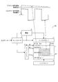
図1は、本発明の一実施形態に係る表示装置100の要部の概略構成を示すブロック図である。
(1-1.表示装置の構成)
図1は、本発明の一実施形態に係る表示装置100の要部の概略構成を示すブロック図である。
図1に示すように、表示装置100は、液晶パネル1(表示パネル)、ゲートドライバ2、ソースドライバ3(信号ドライバ)、電源4、コントローラ5(制御手段)及びバックライト6を備えている。
液晶パネル1は、複数の画素がマトリクス状に配されたアクティブマトリクス型の液晶パネルである。液晶パネル1は、図示しないが、アクティブマトリクス基板と対向基板との間に液晶層が狭持された構造を有している。液晶パネル1としては、透過型の液晶パネルであれば特に限定されるものではなく、公知の液晶パネルを用いることができる。
液晶パネル1には、複数のゲートラインGL(走査線)と複数のソースラインSL(信号線)とが互いに交差して配置されている。これらゲートラインGLとソースラインSLとで囲まれた領域が1画素であり、各画素には表示電極12及びTFT等のスイッチング素子13がそれぞれ設けられている。図2は、表示装置100が備える液晶パネル1の構成を示す図である。
このゲートラインGLはゲートドライバ2に接続され、ソースラインSLはソースドライバ3に接続されている。また、スイッチング素子13のゲート電極、ソース電極及びドレイン電極には、ゲートラインGL、ソースラインSL及び表示電極12がそれぞれ接続されている。
つまり、ソースドライバ3からソースラインSLを介して選択的にスイッチング素子13にソース信号を供給し、ゲートドライバ2からゲートラインGLを介してスイッチング素子13にゲート信号を供給することにより、スイッチング素子13のON/OFFを制御する。
ゲートドライバ2は、コントローラ5から供給されるゲート制御信号に基づいて、各ゲートラインGLに走査順にゲート信号として電圧を供給する。
ソースドライバ3は、コントローラ5から供給されるソース制御信号に基づいて、各ソースラインSLにソース信号を供給する。具体的には、複数のソースラインSLのそれぞれに、液晶パネル1に表示するための画像データを供給する。
電源4は、コントローラ5から供給される制御信号に基づいて、スイッチング素子13に供給するために必要な電圧をゲートドライバ2及びソースドライバ3に印加する。
コントローラ5は、図示しない入力データ供給源から入力データを取得し、該入力データからゲート制御信号及びソース制御信号を生成し、生成したゲート制御信号をゲートドライバ2に供給し、ソース制御信号をソースドライバ3に供給する。
本実施形態では、コントローラ5は画像データを含む入力データを取得し、取得した入力データに含まれる第1の画像データを供給するソースラインSLには、入力データに含まれる第2の画像データを供給するソースラインSLよりも低いフレーム周波数で第1の画像データを供給するようにソースドライバ3を制御する。
具体的には、コントローラ5は、入力データの一部を第1の画像データとし、残部を第2の画像データとする。このときの条件は、特に限定されるものではないが、例えば、画素を構成する3つのサブピクセルそれぞれに対して1ビットから4ビットの画像データを第1の画像データとすればよく、好ましくは第1の画像データは1ビットのデータである。また、それ以外の画像データ、すなわちサブピクセルそれぞれに対して1ビットから4ビットの画像データ以外を第2の画像データとする。
ここで、1ビットの画像データとは「FF」又は「00」のデータであり、RGB3色のカラーパネルに適用した場合、2値8色表示になる。なお、1画素を形成するRGBの各サブピクセルの信号に「FF」又は「00」を入力すると、白又は黒のいずれかの色で表示されるため、モノクロ画像になる。
この画像データはビット数が増えるほど表示する階調数が多くなっていくが、それに伴って画像品位が低下し易くなる。これに対し、例えば、各サブピクセルに入力する信号が1ビットから4ビット(16階調、4096色)程度の低ビットの画像データであれば階調表示数が少ないために画像の品位低下が少ない。
例えば、画素の電圧保持率が99.5%の場合、1フレームにおける電圧降下は4ビット(16階調)のとき、階調毎の電圧差の約7%程度である。通常60Hzであるフレームレートを20Hz(3回に1回書き込み)にしても、その電圧変化量は約20%になり、テキスト表示には問題ないレベルである。
よって、低ビットの画像データを低いフレーム周波数で書き込むことにより、表示品位を損なうことなく、低消費電力を実現することができる。
1ビットから4ビットのデータとしては、例えば、テキストデータ、並びに白、黒及びRGBの原色からなる群より選ばれる少なくとも1つの色によって表示される画像データを含む。この画像データとしては、例えば、書籍(文字、テキスト)、ワープロドキュメント又はアイコン等が挙げられる。
また、1ビットから4ビットのデータ以外の画像データとは、多数の階調によって画像が表示される、すなわち色数が多い多ビットの画像データであり、例えば、5ビット以上のデータである。この第2の画像データによって表示されるものとしては、例えば、写真又はスライドショー等の静止画像又は動画像を含む。
以下の説明において、第1の画像データを表示する領域をテキスト表示領域と称し、第2の画像データを表示する領域をフルカラー表示領域と称する。
例えば、図1中、ソースラインSL1からソースラインSLnまでの範囲と、ゲートラインGL1からゲートラインGLnまでの範囲によって囲まれる領域21がテキスト表示領域である。また、図1中、ソースラインSLnからソースラインSLn+aまでの範囲と、ゲートラインGLnからゲートラインGLn+aまでの範囲によって囲まれる領域20がフルカラー表示領域である。
なお、本明細書では、第1の画像データを表示する領域をテキスト表示領域と称しているが、上述したように、第1の画像データに含まれるアイコン等、低ビットの画像データもテキスト表示領域に表示され得る。
入力データ供給源としては、特に限定されるものではなく、例えば、携帯電話、携帯型ゲーム機、PDA(Personal Digital Assistants)、デジタルカメラ、ノート型パソコン、電子ブック等が挙げられる。
バックライト6は、液晶パネル1の背面側(すなわち、表示面とは反対側)に設けられ、液晶パネル1に光を照射する。バックライト6は特に限定されるものではなく、例えば、LED(発光ダイオード)等の従来公知の発光素子を用いた光源を用いればよい。
なお、本実施形態では、表示装置100がコントローラ5を内蔵している構成であるが、コントローラ5を表示装置100の外部に設ける構成であってもよい。また、ゲートドライバ2及びソースドライバ3が液晶パネル1の外部に設ける構成であるが、ゲートドライバ2及びソースドライバ3のうち少なくとも一つを液晶パネル1と一体的に形成してもよい。
(1-2.フレーム周波数の制御)
次に、本実施形態におけるフレーム周波数の制御方法(制御ステップ)について説明する。
次に、本実施形態におけるフレーム周波数の制御方法(制御ステップ)について説明する。
表示装置100において、入力データ供給源からコントローラ5に入力される入力データには、テキストデータ等の画像データ、水平同期信号及び垂直同期信号等の制御信号とが含まれている。コントローラ5は、入力データ供給源から水平同期信号及び垂直同期信号等の制御信号を取得し、取得した制御信号に基づいてゲート制御信号及びソース制御信号を生成して、ゲートドライバ2及びソースドライバ3にそれぞれ供給する。
このゲート制御信号はゲートドライバ2の駆動のタイミングを制御するためのタイミング信号であり、ゲートスタートパルス、ゲートシフトクロック、ゲート出力イネーブル等が含まれる。また、データ制御信号はソースドライバ3の駆動のタイミングを制御するためのタイミング信号であり、ソーススタートパルス、ソースシフトクロック、ソース出力イネーブル、極性反転信号等が含まれる。
また、上述したように、コントローラ5は、液晶パネル1に表示するための画像データを含む入力データを取得すると、取得した入力データのうち、第1の画像データと第2の画像データとで、複数のソースラインSLのそれぞれに画像データを供給する際のフレーム周波数を変えている。
具体的には、取得した入力データが画素を構成する3つのサブピクセルそれぞれに対して1ビットから4ビット程度の低ビットのデータであれば第1の画像データ、それ以上のビット数のデータであれば第2の画像データと判断し、第1の画像データと判断したデータを供給するソースラインSLには、第2の画像データと判断したデータを供給するソースラインSLよりも低いフレーム周波数で供給する。
一般に、例えば1ビットから4ビット程度の低ビットの画像データは階調表示数が少ないため、多階調を表示するデータよりも画質の品位低下が少ない。よって、低ビットの画像データを低いフレーム周波数で書き込んだとしても、表示品位を損なうことがない。
また、表示パネルとして液晶パネル1を用いた場合、一般的にデータ信号を書き込む際に極性を正負反転させるが、この極性反転において電力が消費される。
本実施形態によれば、第1の画像データは画質の品位低下が少ないため、第2の画像データをソースラインSLに供給するフレーム周波数よりも低くすることができる。よって、第1の画像データによる極性反転の数が減ると共に、第1の画素データをソースラインSLに供給するソースドライバ3の駆動電力も抑えることができる。したがって、低消費電力を実現することができる。
ここで、フレーム周波数(Hz)とは、1秒間当たりに書き換えるフレームの数を表す。なお、本実施形態では通常(すなわち、フレーム周波数を下げていない状態)のフレーム周波数を60Hzとする。また、フレームの書き換えを「書き込み」又は「リフレッシュ」ともいう。
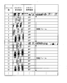
本実施形態におけるテキスト表示領域とフルカラー表示領域とのフレーム周波数の比較を図3に示す。図3は、表示装置100におけるテキスト表示領域とフルカラー表示領域とのフレーム周波数の比較を示す表である。
図3の表において、「ON」、「OFF」はソースラインSLに画像データを供給しているか否かを表している。
この表に示すように、フルカラー表示領域では、毎フレーム書き換えを行なっている。一方、テキスト表示領域では始めのフレーム1では書き換えを行なっているが、フレーム2からフレーム10までは待機フレーム(休止フレーム)としており、書き換えを行なっていない。
つまり、テキスト表示領域を書き込むフレームの周期は10周期であり、このときのフレーム周波数はフルカラー表示領域のフレーム周波数の10分の1である。
表示パネルの仕様等にもよるが、ここでは、全画面がフルカラー表示領域(すなわち、通常のフレーム周波数で表示される)である場合に消費される電力が、1フレームあたり10mWの液晶パネル1を例に説明する。
図4は、クロック発生器の発振周波数と消費電力との関係を示すグラフであり、グラフの横軸は発振周波数(Hz)を示し、縦軸は表示パネルにおける消費電力(mW)を示す。
液晶パネル1の全画面がテキスト表示の場合、1フレームは「ON」にするため、消費電力は10mWになる。次に、2フレームから10フレームまでは「OFF」にするが、このとき書き込みタイミングを決めるためのタイミングクロック等は常時動作しているため、消費電力は0mWにはならず、図4のグラフ中矢印で示すように、例えばクロック周波数が約500KHzの場合には概ね2mWになる。
したがって、この場合の平均消費電力は(10+2×9)/10=2.8mWになり、フルカラー表示の場合と比較して約70%の消費電力を削減できる。
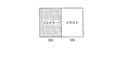
そのため、例えば液晶パネル1の全画面に対するフルカラー表示領域とテキスト表示領域との割合が、図5に示すように50%ずつである場合、画面全体における消費電力は平均約5.4mWになる。すなわち、全画面がフルカラー表示領域である場合と比較して、40%以上消費電力を削減できる。図5は、表示装置100が備える液晶パネル1の全画面に対するフルカラー表示領域とテキスト表示領域との割合を示す図である。
特に、表示装置100を電子ブックとして利用する場合、全画面の80%以上がテキスト表示で作業され得る。そのため、フルカラー表示に対して60%以上消費電力を削減できる。
その後、フレーム11ではテキスト表示領域も書き換えを行なうため、全画素にデータが書き込まれることになる。なお、テキスト表示領域の書き換えを行なわないことを「待機」、「休止」又は「非リフレッシュ」ともいう。
(1-3.リフレッシュ)
一般的に、中間調を表示する場合には毎フレーム書き換えなくては画質を維持することができない。言い換えれば、フルカラー表示領域の画素は電圧の保持率が低い。そのため、フルカラー表示領域では、図6に示すように、フレーム毎に画素電位を反転させて交流化駆動させている。図6は、テキスト表示領域の画素電位の保有率とフルカラー表示領域の画素電位の保有率とをする図である。
一般的に、中間調を表示する場合には毎フレーム書き換えなくては画質を維持することができない。言い換えれば、フルカラー表示領域の画素は電圧の保持率が低い。そのため、フルカラー表示領域では、図6に示すように、フレーム毎に画素電位を反転させて交流化駆動させている。図6は、テキスト表示領域の画素電位の保有率とフルカラー表示領域の画素電位の保有率とをする図である。
これに対し、本実施形態においてテキスト表示領域に表示するテキストデータが例えば1ビットのデータであれば、中間調を表示しない。そのため、トランジスタの性能に依存するが、1フレーム毎に保持電圧が低下する割合は例えば1%程度であり、画素電位の保有率低下は図6に示すように緩やかである。
ここで、テキストデータを書き込んだとき(リフレッシュしたとき)の電圧保持率を100%とすると、90%までの保持率低下であれば、ユーザは不具合なくテキストを読むことができる。よって、テキスト表示領域では、フレームを頻繁に書き換えなくても一定の画質を維持することができる。
また、上述したように、全画素の書き込みを行なう場合の消費電力と比較して、テキスト表示領域の画素書き込みを数フレームに1回とすることにより、従来の液晶パネル1の全画面を書き換える形態と比較して、図7及び図8に示すように平均消費電力を低減することができる。図7は、表示装置100において液晶パネル1のデータ書き換えにかかる平均消費電力を示す図であり、図8は、テキスト表示領域及びフルカラー表示領域それぞれのデータ書き換えにかかる平均消費電力を示す図である。
なお、図8のテキスト表示領域では、非リフレッシュ期間の消費電力が2mWであり、リフレッシュ期間の消費電力が10mWであり、これらの期間の平均が2.8mWであることを示す。また、図7に示す液晶パネル1のデータ書き換えにかかる平均消費電力は、図8に示すテキスト表示領域及びフルカラー表示領域それぞれのデータ書き換えにかかる平均消費電力を平均したものである。
このように、表示装置100によれば、フルカラー表示領域では毎フレーム書き換えを行なうために表示品位を落とすことがなく、テキスト表示領域ではフルカラー表示領域よりもフレーム周波数を低くして書き換え数を減らすことによって、消費電力を低減することができる。
さらに、例えば、図6に示すゲートラインGL1~GLnでは、ライン上にフルカラー表示領域がない。そのため、このゲートラインGL1~GLnに対しては、ゲートドライバ2はOFFの電圧を出し続ければよく、ゲートドライバ2の消費電力を低減することができる。
このとき、ソースドライバ3はOFFの固定電位をかければよいため、ゲートラインGL1~GLn上の領域における画素の電位差が変動しない。よって、画素変位に伴って消費される電力も低減することができる。
(1-4.休止フレームのリセット)
ところで、上述した非リフレッシュ期間に第1の画像データの書き換え指示を含む入力データを取得することがある。そのため、表示装置100が、第1の画像データを供給しない休止フレーム(待機フレームともいう)期間をカウントするカウント手段を備えていることが好ましい。
ところで、上述した非リフレッシュ期間に第1の画像データの書き換え指示を含む入力データを取得することがある。そのため、表示装置100が、第1の画像データを供給しない休止フレーム(待機フレームともいう)期間をカウントするカウント手段を備えていることが好ましい。
ここでいう「休止フレーム期間」とは、予め定められた休止フレームの数だけデータの書き込みを行なわない期間である。
つまり、コントローラ5は、休止フレームにおいて第1の画像データの書き換え指示を含む入力データを取得したとき、休止フレームの次のフレームにおいて第1の画像データを供給するようにソースドライバ3を制御し、カウント手段は、次のフレームから新たに休止フレーム期間をカウントすることができる。
本実施形態では、上述したようにテキスト表示領域への書き込みを10周期としている。このとき、図9に示すように、待機フレーム期間中にテキスト書き換え指示を取得した場合(フレーム6)、コントローラ5は、テキスト書き換え指示を取得したフレームの次のフレーム(フレーム7)で第1の画像データを供給するようにソースドライバ3を制御する。これにより、フレーム7では全画素の書き込みが行なわれる。
図9は、表示装置100におけるテキスト表示領域とフルカラー表示領域とのフレーム周波数の比較を示す表である。
このように全画素の書き込みが行なわれると、カウント手段は、フレーム7から新たに休止フレーム期間をカウントする。よって、書き換え後に速やかに所定の休止フレーム期間を始めから再開することができる。
なお、カウント手段の機能はコントローラ5が有していてもよいし、別途カウント手段を備える構成であってもよい。
また、第1の画像データの書き換え指示は、第1の画像データのサイズ変更指示を含んでいてもよい。
例えば、液晶パネル1の全画面に対するフルカラー表示領域とテキスト表示領域との割合が50%ずつであるときに(図10の(a))、テキスト表示領域のサイズを70%に拡大するという指示を取得した場合、コントローラ5は、サイズ変更指示を取得したフレームの次のフレームで全画素の書き込みを行なうようにソースドライバ3を制御する。
これにより、テキスト表示領域のサイズが70%であり、フルカラー表示領域が30%である割合でそれぞれの画像データが表示される(図10の(b))。図10は、表示装置100が備える液晶パネル1の全画面に対するフルカラー表示領域とテキスト表示領域との割合を示す図である。
この場合も、カウント手段は、全画素の書き込みを行なったフレームから新たに休止フレーム期間をカウントする。よって、休止フレーム期間にサイズ変更指示を取得しても、サイズ変更後に速やかに所定の休止フレーム期間を始めから再開することができる。
(1-5.テキストデータの変換)
次に、本実施形態において、入力データに多階調のテキストデータが含まれる場合のデータ変換方法について、図11及び図12を参照して説明する。
次に、本実施形態において、入力データに多階調のテキストデータが含まれる場合のデータ変換方法について、図11及び図12を参照して説明する。
図11は、表示装置100の変形例を示すブロック図であり、図12は、多階調のテキストデータを1ビットのテキストデータに変換する際の処理の流れを示すフローチャートである。
表示装置100は、図11に示すように、入力データに、多階調のテキストデータが含まれるか否かを判定し、多階調のテキストデータが含まれる場合、当該テキストデータをサブピクセル一つ当たり1ビット~4ビットのデータに変換するCPU7(central processing unit、変換手段)をさらに備えていてもよい。この場合、コントローラ5は、CPU7によって変換されたテキストデータを第1の画像データとする。
例えば、入力データには多階調のテキストデータが含まれることがある。つまり、文字(テキストデータ)が白、黒及びRGBの原色からなる群より選ばれる少なくとも1つの色によって表示されるデータではなく、緑又は黄色などの中間調の色によって表示されるデータであることがある。
そのため、入力データに、多階調のテキストデータが含まれるか否かを判定し、多階調のテキストデータが含まれる場合にサブピクセル一つ当たり1ビット~4ビットのデータに変換することにより、より低いフレーム周波数で駆動することが可能な領域が増える。
本実施形態では、図12に示すように、まず、CPU7が入力データ供給源から入力データを取得し(ステップS1)、取得した入力データにテキストデータが含まれるか否かを判定する(ステップS2)。
ここで、テキストデータが含まれていると判定した場合(ステップS2にて「YES」)、CPU7は、さらに、テキストデータが、サブピクセル一つ当たり1ビット~4ビットのテキストデータであるか、多階調のテキストデータであるかを判定する(ステップS3)。
一方、テキストデータが含まれていないと判定した場合(ステップS2にて「NO」)、コントローラ5はアイコン等の第1の画像データと判定した入力データに関しては上述したように低いフレーム周波数で駆動し、第2の画像データと判定した入力データに関しては毎フレーム書き換える(ステップS4)。
ステップS3にて多階調のテキストデータであると判定した場合、CPU7は、多階調のテキストデータを1ビットのデータに変換する(ステップS5)。
1ビットのデータへの変換方法は特に限定されるものではなく、例えば、多階調のテキストデータであると判定した場合は、該データの階調に関係なく、すべてモノクロで表示するように変換してもよい。
例えば、256階調のデータが入力された場合、1ビット変換のスライスレベルを任意に設定しておくことによって、強制的に多階調のデータを1ビットのデータに変換することができる。例えば、0~16階調までのデータを「0」、すなわち黒に変換し、17~255階調までのデータを「1」、すなわち白に変換して出力する。これにより、多階調のテキストデータが入力されたとしても、低いフレーム周波数で駆動させることができる。
なお、ここでは多階調のテキストデータを1ビットのデータに変換する例を挙げているが、これに限定されるものではなく、例えば2ビットに変換する場合も同様の方法を適用することができる。この場合にも、画質の劣化を伴わずに、書き換えフレームを低減することができる。
その後、コントローラ5は、CPU7によって変換されたテキストデータを第1の画像データとし、第2の画像データよりも低いフレーム周波数で駆動するようにソースドライバ3を制御する(ステップS6)。
例えば、入力データに多階調のテキストデータが含まれる場合、上述したような変換処理を行なわない場合には、多階調のテキストデータを第2の画像データであるとして、毎フレーム書き換えるように制御してしまう。
そこで、入力データに多階調のテキストデータが含まれるか否かを判定し、多階調のテキストデータが含まれていれば、例えば1ビットのデータに変換することにより、より低いフレーム周波数で駆動することが可能な領域が増える。よって、さらに消費電力を低減することができる。
なお、本実施形態ではCPU7がデータの変換機能(テキスト有り無し判定を含む)を有しているが、この形態に限定されるものではない。例えば、コントローラがデータの変換機能を有していてもよいし、該機能を有する他の部材を内蔵してもよい。また、外付けの装置においてデータの変換を行なってもよい。
(1-6.第1の画像データの書き込み周期)
ここで、図13を参照して、第1の画像データを書き込む周期の設定について説明する。図13は、表示装置100におけるテキスト表示領域とフルカラー表示領域とのフレーム周波数の比較を示す表である。
ここで、図13を参照して、第1の画像データを書き込む周期の設定について説明する。図13は、表示装置100におけるテキスト表示領域とフルカラー表示領域とのフレーム周波数の比較を示す表である。
上述した実施形態では、第1の画像データを書き込むフレームを10周期毎にしているが、例えば、フレーム毎に画像データの書き込み極性を反転させる場合、第1の画像データを書き込むフレームを10周期にした場合、データの書き込み極性が常に一方に偏ってしまう。
つまり、10周期でデータを書き込む場合、図13の表に示すように、最初に第1の画像データを書き込むフレーム1では「+」の極性であり、次にデータを書き込むフレーム11では「+」の極性であり、さらにデータを書き込むフレーム21では「+」の極性である。
このように、データの書き込み極性が常に一方に偏ってしまうと、液晶パネル1では「焼きつき」が生じ、短寿命となる。
そこで、コントローラ5は、第1の画像データ及び第2の画像データを同時に供給してから、次回、第1の画像データ及び第2の画像データを同時に供給するまでに第2の画像データのみを偶数フレーム供給するように制御することが好ましい。これにより、一定の極性に偏らずに画像データを書き込むことできるため、焼きつきの発生を抑えることができる。
例えば、図13の表では、第1の画像データの書き込み周期を5周期としている。そのため、最初に第1の画像データを書き込むフレーム1では「+」の極性であり、次にデータを書き込むフレーム6では「-」の極性であり、次にデータを書き込むフレーム11では「+」の極性であり、さらにデータを書き込むフレーム16では「-」の極性である。
このように、第1の画像データの書き込むフレームでは、毎回極性が反転するように書き込んでいるため、焼きつきの発生を抑え、長寿命になる。
なお、本実施形態ではフレームの書き込み周期を固定させているが、例えば、一定の期間が経過した後に異なる書き込み周期に変更されるように制御してもよい。
また、液晶パネル1がノーマリーホワイトモードである場合、テキスト表示領域の背景を白表示にし、文字を黒表示にすることにより、文字の部分のみを駆動させればよいため、駆動領域を最小化できる。よって、ゲートドライバ2の消費電力を低減することができる。
一方、液晶パネル1がノーマリーブラックモードである場合、テキスト表示領域の背景を黒表示にし、文字を白表示にすることにより、文字の部分のみを駆動させればよいため、駆動領域を最小化できる。よって、ゲートドライバ2の消費電力を低減することができる。
このように、表示装置100によれば、表示品位が低下し易い第2の画像データは毎フレーム書き換え、表示品位が低下し難い第1の画像データのフレーム周波数を低下させることにより、表示品位を損なうことがない。また、第1の画像データのフレーム周波数を低下させることにより、データの書き換えに要する消費電力を低減することができる。
さらに、表示装置100では、フレーム周波数を落とす第1の画像データを表示する領域は固定されず、取得した入力データに応じて、都度、表示領域を変えている。また、フレーム周波数を落とすのは、文字又はアイコン等、画素電位の保有率低下が少ないデータである。よって、何もデータを表示しない非表示領域が生じるものではないため、画面全体の表示領域を狭くすることがない。
また、文字又はアイコン等は画素電位の保有率低下が少ないため、これらのデータを画素に保有しておくためのメモリ等を備える必要がない。よって、従来の表示パネルと比較して開口率が低下することがないため、画面全体が暗くならない。
〔第2の実施形態〕
本発明の表示装置に関する他の一実施形態について説明する。第2の実施形態では、表示パネルとして有機ELパネルを用いている以外は、第1の実施形態にて説明した図面と同じ機能を有する部材を備えているため、その説明を省略する。
本発明の表示装置に関する他の一実施形態について説明する。第2の実施形態では、表示パネルとして有機ELパネルを用いている以外は、第1の実施形態にて説明した図面と同じ機能を有する部材を備えているため、その説明を省略する。
図14は、本発明の他の一実施形態に係る表示装置が備える有機EL(electro luminescence)パネルの等価回路の構成を示す図である。
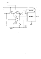
図14に示すように、有機ELパネルの構造は、2つのトランジスタ33,34と1つのキャパシタ36とを備えた構造である。具体的には、データ線30と走査線31との交差部にスイッチング用のNMOS・TFT33(以下、Tr1という)が配置され、駆動用のPMOS・TFT34(以下、Tr2という)に電源を供給するための電源供給線32が配されている。
信号ライン30と走査ライン31との交差部のTr1をオンにすると、キャパシタ36が充電され、有機EL素子35を発光させるためにTr2をオンにしている間、電源供給線32から電流が供給されると有機EL素子35が発光する。
表示装置100が有機ELパネルを備える場合、テキスト表示領域の背景を黒表示にし、文字を白表示にすることにより、駆動領域を最小化できる。よって、液晶パネル1と同様にゲートドライバ2の消費電力を低減することができる。
また、テキスト表示領域の背景が黒表示であればその領域を発光させる必要がなく、Tr1及びTr2は共に駆動する必要がない。また、キャパシタ36の充電が終了した後はTr1をオンにする必要がない。よって、消費電力を低減できる。テキスト表示領域における文字は白表示に限定されるものではなく、RGB単色であってもよい。
なお、キャパシタ36の自由放電があるため、液晶と同様に数フレームに1回は書き換える必要がある。例えば、図15に示すように、第1の実施形態と同様に、フルカラー表示領域が毎フレーム画素を書き換えるのに対し、テキスト表示領域では画素の書き換えを数フレーム周期で行なう。図15は、本発明の他の一実施形態に係る表示装置におけるテキスト表示領域とフルカラー表示領域とのフレーム周波数の比較を示す表である。
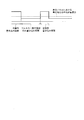
ここでは、テキスト表示領域の書き込みフレームではTr1をONにし、待機フレームではTr1をOFFしており、フルカラー表示領域の10分の1のフレーム周波数で書き換えを行なっている。このときの駆動電圧及び素子発光強度について図16を参照して説明する。図16は、Tr1のON/OFFに伴う駆動電圧及び素子発光強度を示す図である。
図16において、「Tr1オン/オフ」のタイミングは図15に示すTr1のオン/オフのタイミングと同期している。すなわち、図16はテキスト表示領域のTr1の動作を表している。
この例のテキスト表示領域では、10フレームに1回Tr1をオンしており、Tr1に繋がっているキャパシタの電圧は、有機ELの発光を制御するTr2のゲート電圧を10フレーム維持できる。
なお、本実施形態では、テキスト表示領域の背景を黒表示し、文字(テキスト又はアイコン等)を白表示又はカラー表示するため、図16に示すように、有機EL素子35の発光強度を維持しつつフレーム周波数を低減できる。
また、液晶パネル1と同様に全画面をフルカラー表示領域とテキスト表示領域とに分けることにより、テキスト表示領域の書き換えを毎フレーム行なわなくてもよいため、消費電力を低減することができる。図17は、テキスト表示領域及びフルカラー表示領域それぞれのデータ書き換えにかかる平均消費電力を示す図である。
このように、有機ELパネルを用いた場合にも、液晶パネル1と同様にテキスト表示領域の書き換えを毎フレーム行なわなくても表示品位を損なうことなく、また、駆動電圧を下げることができるため、消費電力の低減を実現することができる。
(プログラム及び記録媒体)
最後に、表示装置100に含まれている各部は、ハードウェアロジックによって構成すればよい。又は、次のように、CPUを用いてソフトウェアによって実現してもよい。
最後に、表示装置100に含まれている各部は、ハードウェアロジックによって構成すればよい。又は、次のように、CPUを用いてソフトウェアによって実現してもよい。
すなわち表示装置100は、各機能を実現するプログラムの命令を実行するCPU、このプログラムを格納したROM、上記プログラムを実行可能な形式に展開するRAM、及び、上記プログラム及び各種データを格納するメモリ等の記憶装置(記録媒体)を備えている。この構成により、本発明の目的は、所定の記録媒体によっても達成できる。
この記録媒体は、上述した機能を実現するソフトウェアである表示装置100のプログラムのプログラムコード(実行形式プログラム、中間コードプログラム、ソースプログラム)をコンピュータで読み取り可能に記録していればよい。表示装置100に、この記録媒体を供給する。これにより、コンピュータとしての表示装置100(又はCPUやMPU)が、供給された記録媒体に記録されているプログラムコードを読み出し、実行すればよい。
プログラムコードを表示装置100に供給する記録媒体は、特定の構造又は種類のものに限定されない。すなわちこの記録媒体は、例えば、磁気テープ又はカセットテープ等のテープ系、フロッピー(登録商標)ディスク/ハードディスク等の磁気ディスク又はCD-ROM/MO/MD/DVD/CD-R等の光ディスクを含むディスク系、ICカード(メモリカードを含む)/光カード等のカード系、もしくはマスクROM/EPROM/EEPROM/フラッシュROM等の半導体メモリ系などとすることができる。
また、表示装置100を通信ネットワークと接続可能に構成しても、本発明の目的を達成できる。この場合、上記のプログラムコードを、通信ネットワークを介して表示装置100に供給する。この通信ネットワークは表示装置100にプログラムコードを供給できるものであればよく、特定の種類又は形態に限定されない。例えばインターネット、イントラネット、エキストラネット、LAN、ISDN、VAN、CATV通信網、仮想専用網(Virtual Private Network)、電話回線網、移動体通信網、衛星通信網等であればよい。
この通信ネットワークを構成する伝送媒体も、プログラムコードを伝送可能な任意の媒体であればよく、特定の構成又は種類のものに限定されない。例えばIEEE1394、USB、電力線搬送、ケーブルTV回線、電話線、ADSL(Asymmetric Digital Subscriber Line)回線等の有線でも、IrDAやリモコンのような赤外線、Bluetooth(登録商標)、802.11無線、HDR、携帯電話網、衛星回線、地上波デジタル網等の無線でも利用可能である。
本発明は上述した実施形態に限定されるものではなく、請求項に示した範囲で種々の変更が可能であり、実施形態に開示された技術的手段を適宜組み合わせて得られる実施形態についても本発明の技術的範囲に含まれる。
(その他)
また、本発明の一態様に係る表示装置では、上記表示パネルの各画素はRGB3つのサブピクセルから構成されており、上記制御手段は、上記入力データのうち、上記サブピクセル一つ当たり1ビットから4ビットで割り当てられる画像データを上記第1の画像データとし、上記サブピクセル一つ当たり1ビットから4ビットで割り当てられる画像データ以外を上記第2の画像データとして、上記信号ドライバを制御することが好ましい。
(その他)
また、本発明の一態様に係る表示装置では、上記表示パネルの各画素はRGB3つのサブピクセルから構成されており、上記制御手段は、上記入力データのうち、上記サブピクセル一つ当たり1ビットから4ビットで割り当てられる画像データを上記第1の画像データとし、上記サブピクセル一つ当たり1ビットから4ビットで割り当てられる画像データ以外を上記第2の画像データとして、上記信号ドライバを制御することが好ましい。
上記の構成によれば、取得した入力データのうち、サブピクセル一つ当たり1ビットから4ビットの画像データであれば第1の画像データとして、より低いフレーム周波数で画像データを信号線に供給するように制御し、それ以外の画像データであれば第2の画像データとして、通常のフレーム周波数で画像データを信号線に供給するように制御する。
1ビットの画像データとは「FF」又は「00」のデータであり、RGB3色のカラーパネルに適用した場合、2値8色表示になる。なお、1画素を形成するRGBの各サブピクセルの信号に「FF」又は「00」を入力すると、白又は黒のいずれかの色で表示されるため、モノクロ画像になる。
この画像データはビット数が増えるほど表示する階調数が多くなっていくが、それに伴って画像品位が低下し易くなる。これに対し、例えば、各サブピクセルに入力する信号が1ビットから4ビット(16階調、4096色)程度の低ビットの画像データであれば階調表示数が少ないために画像の品位低下が少ない。
よって、低ビットの画像データを低いフレーム周波数で書き込むことにより、表示品位を損なうことなく、低消費電力を実現することができる。
また、本発明の一態様に係る表示装置では、上記入力データに、多階調のテキストデータが含まれるか否かを判定し、多階調のテキストデータが含まれる場合、当該テキストデータを上記サブピクセル一つ当たり1ビット~4ビットのデータに変換する変換手段を備え、上記制御手段は、上記変換手段によって変換されたテキストデータを上記第1の画像データとすることが好ましい。
例えば、入力データには多階調のテキストデータが含まれることがある。そのため、入力データに、多階調のテキストデータが含まれるか否かを判定し、多階調のテキストデータが含まれる場合に1ビット~4ビットのデータに変換することにより、より低いフレーム周波数で駆動することが可能な領域が増える。よって、さらに消費電力を低減することができる。
また、本発明の一態様に係る表示装置では、上記制御手段は、上記第1の画像データ及び第2の画像データを同時に供給してから、次回、上記第1の画像データ及び第2の画像データを同時に供給するまでに上記第2の画像データのみを偶数フレーム供給するように制御することが好ましい。
例えば、フレーム毎に画像データの書き込み極性を反転させる場合、第1の画像データを書き込むフレームを10周期等にした場合、データの書き込み極性が常に一方に偏ってしまう。この場合、例えば液晶パネルでは「焼きつき」が生じ、短寿命となる。
そこで、第1の画像データ及び第2の画像データを同時に供給してから、第2の画像データのみを偶数フレーム供給し、再び第1の画像データ及び第2の画像データを同時に供給する。これにより、一定の極性に偏らずに画像データを書き込むことできるため、焼きつきの発生を抑えることができる。
また、本発明の一態様に係る表示装置では、上記第1の画像データを供給しない休止フレーム期間をカウントするカウント手段を備え、上記制御手段は、休止フレームにおいて上記第1の画像データの書き換え指示を含む入力データを取得したとき、上記休止フレームの次のフレームにおいて上記第1の画像データを供給するように上記信号ドライバを制御し、上記カウント手段は、上記次のフレームから新たに上記休止フレーム期間をカウントすることが好ましい。
これにより、例えば、休止フレーム期間に第1の画像データの書き換え指示が来たとしても、書き換え後に速やかに休止フレーム期間を始めから再開することができる。
また、上記書き換え指示は、上記第1の画像データのサイズ変更指示を含むことが好ましい。
これにより、例えば、休止フレーム期間に第1の画像データのサイズ変更指示が来たとしても、書き換え後に速やかに休止フレーム期間を始めから再開することができる。
また、本発明の一態様に係る表示装置では、上記表示パネルは、液晶表示パネル又は有機EL表示パネルであることが好ましい。
上記の構成によれば、多階調のカラー表示を好適に行なうことができると共に、消費電力を低減することができる。
なお、上記表示装置は、コンピュータによって実現してもよい。この場合、コンピュータを上記各手段として動作させるためのプログラム、及びそのプログラムを記録したコンピュータ読み取り可能な記録媒体も、本発明の範疇に入る。
本発明は、例えば、液晶パネル又は有機ELパネルを備えた電子ペーパー、携帯電話、電子辞書等の表示装置に好適に利用することができる。
1 液晶パネル(表示パネル)
2 ゲートドライバ
3 ソースドライバ(信号ドライバ)
4 電源
5 コントローラ(制御手段)
6 バックライト
7 CPU(変換手段)
13 スイッチング素子
100 表示装置
2 ゲートドライバ
3 ソースドライバ(信号ドライバ)
4 電源
5 コントローラ(制御手段)
6 バックライト
7 CPU(変換手段)
13 スイッチング素子
100 表示装置
Claims (10)
- 複数の走査線と複数の信号線とが互いに交差して配置された表示パネルと、
上記複数の信号線のそれぞれに、上記表示パネルに表示するための画像データを供給する信号ドライバと、
上記画像データを含む入力データを取得し、取得した入力データに含まれる第1の画像データを供給する上記信号線には、上記入力データに含まれる第2の画像データを供給する上記信号線よりも低いフレーム周波数で上記第1の画像データを供給するように上記信号ドライバを制御する制御手段とを備え、
上記制御手段は、上記入力データの一部を上記第1の画像データとし、残部を上記第2の画像データとすることを特徴とする表示装置。 - 上記表示パネルの各画素はRGB3つのサブピクセルから構成されており、
上記制御手段は、上記入力データのうち、上記サブピクセル一つ当たり1ビットから4ビットで割り当てられる画像データを上記第1の画像データとし、上記サブピクセル一つ当たり1ビットから4ビットで割り当てられる画像データ以外を上記第2の画像データとして、上記信号ドライバを制御することを特徴とする請求項1に記載の表示装置。 - 上記入力データに、多階調のテキストデータが含まれるか否かを判定し、多階調のテキストデータが含まれる場合、当該テキストデータを上記サブピクセル一つ当たり1ビット~4ビットのデータに変換する変換手段を備え、
上記制御手段は、上記変換手段によって変換されたテキストデータを上記第1の画像データとすることを特徴とする請求項2に記載の表示装置。 - 上記制御手段は、上記第1の画像データ及び第2の画像データを同時に供給してから、次回、上記第1の画像データ及び第2の画像データを同時に供給するまでに上記第2の画像データのみを偶数フレーム供給するように制御することを特徴とする請求項1~3のいずれか1項に記載の表示装置。
- 上記第1の画像データを供給しない休止フレーム期間をカウントするカウント手段を備え、
上記制御手段は、休止フレームにおいて上記第1の画像データの書き換え指示を含む入力データを取得したとき、上記休止フレームの次のフレームにおいて上記第1の画像データを供給するように上記信号ドライバを制御し、
上記カウント手段は、上記次のフレームから新たに上記休止フレーム期間をカウントすることを特徴とする請求項1~4のいずれか1項に記載の表示装置。 - 上記書き換え指示は、上記第1の画像データのサイズ変更指示を含むことを特徴とする請求項5に記載の表示装置。
- 上記表示パネルは、液晶パネル又は有機ELパネルであることを特徴とする請求項1~6のいずれか1項に記載の表示装置。
- 複数の走査線と複数の信号線とが互いに交差して配置された表示パネルと、上記複数の信号線のそれぞれに、上記表示パネルに表示するための画像データを供給する信号ドライバとを備える表示装置の制御方法であって、
上記画像データを含む入力データを取得し、取得した入力データに含まれる第1の画像データを供給する上記信号線には、上記入力データに含まれる第2の画像データを供給する上記信号線よりも低いフレーム周波数で上記第1の画像データを供給するように上記信号ドライバを制御する制御ステップを含み、
上記制御ステップでは、上記入力データの一部を上記第1の画像データとし、残部を上記第2の画像データとすることを特徴とする制御方法。 - 請求項1~7のいずれか1項に記載の表示装置の各手段としてコンピュータを動作させるためのプログラム。
- 請求項9に記載のプログラムを記載したコンピュータ読み取り可能な記録媒体。
Applications Claiming Priority (2)
| Application Number | Priority Date | Filing Date | Title |
|---|---|---|---|
| JP2010-150274 | 2010-06-30 | ||
| JP2010150274 | 2010-06-30 |
Publications (1)
| Publication Number | Publication Date |
|---|---|
| WO2012002258A1 true WO2012002258A1 (ja) | 2012-01-05 |
Family
ID=45401976
Family Applications (1)
| Application Number | Title | Priority Date | Filing Date |
|---|---|---|---|
| PCT/JP2011/064473 Ceased WO2012002258A1 (ja) | 2010-06-30 | 2011-06-23 | 表示装置及びその制御方法、プログラム並びに記録媒体 |
Country Status (1)
| Country | Link |
|---|---|
| WO (1) | WO2012002258A1 (ja) |
Cited By (3)
| Publication number | Priority date | Publication date | Assignee | Title |
|---|---|---|---|---|
| CN103680382A (zh) * | 2012-09-24 | 2014-03-26 | 三星显示有限公司 | 显示器驱动方法及其集成驱动设备 |
| KR20200015645A (ko) * | 2020-01-28 | 2020-02-12 | 삼성디스플레이 주식회사 | 표시 장치 및 표시 장치의 구동 방법 |
| KR20200145801A (ko) * | 2020-01-28 | 2020-12-30 | 삼성디스플레이 주식회사 | 표시 장치 및 표시 장치의 구동 방법 |
Citations (5)
| Publication number | Priority date | Publication date | Assignee | Title |
|---|---|---|---|---|
| JPH07152340A (ja) * | 1993-11-30 | 1995-06-16 | Rohm Co Ltd | ディスプレイ装置 |
| JP2001242818A (ja) * | 2000-02-28 | 2001-09-07 | Nec Corp | 表示装置、携帯用電子機器および表示装置の駆動方法 |
| JP2002229547A (ja) * | 2001-02-07 | 2002-08-16 | Hitachi Ltd | 画像表示システム及び画像情報伝送方法 |
| JP2003058130A (ja) * | 2001-06-04 | 2003-02-28 | Seiko Epson Corp | 表示制御回路、電気光学装置、表示装置及び表示制御方法 |
| WO2005078697A1 (ja) * | 2004-02-17 | 2005-08-25 | Sharp Kabushiki Kaisha | 表示装置およびそれを備えた自動車両 |
-
2011
- 2011-06-23 WO PCT/JP2011/064473 patent/WO2012002258A1/ja not_active Ceased
Patent Citations (5)
| Publication number | Priority date | Publication date | Assignee | Title |
|---|---|---|---|---|
| JPH07152340A (ja) * | 1993-11-30 | 1995-06-16 | Rohm Co Ltd | ディスプレイ装置 |
| JP2001242818A (ja) * | 2000-02-28 | 2001-09-07 | Nec Corp | 表示装置、携帯用電子機器および表示装置の駆動方法 |
| JP2002229547A (ja) * | 2001-02-07 | 2002-08-16 | Hitachi Ltd | 画像表示システム及び画像情報伝送方法 |
| JP2003058130A (ja) * | 2001-06-04 | 2003-02-28 | Seiko Epson Corp | 表示制御回路、電気光学装置、表示装置及び表示制御方法 |
| WO2005078697A1 (ja) * | 2004-02-17 | 2005-08-25 | Sharp Kabushiki Kaisha | 表示装置およびそれを備えた自動車両 |
Cited By (10)
| Publication number | Priority date | Publication date | Assignee | Title |
|---|---|---|---|---|
| CN103680382A (zh) * | 2012-09-24 | 2014-03-26 | 三星显示有限公司 | 显示器驱动方法及其集成驱动设备 |
| EP2711919A1 (en) * | 2012-09-24 | 2014-03-26 | Samsung Display Co., Ltd. | Display driving method and integrated driving apparatus thereof |
| KR20140039524A (ko) * | 2012-09-24 | 2014-04-02 | 삼성디스플레이 주식회사 | 표시 장치의 구동 방법 및 표시 장치의 구동 장치 |
| JP2014067032A (ja) * | 2012-09-24 | 2014-04-17 | Samsung Display Co Ltd | 表示装置の駆動方法及び表示装置の駆動装置 |
| US9613554B2 (en) | 2012-09-24 | 2017-04-04 | Samsung Display Co., Ltd. | Display driving method and integrated driving apparatus thereof |
| KR102072781B1 (ko) * | 2012-09-24 | 2020-02-04 | 삼성디스플레이 주식회사 | 표시 장치의 구동 방법 및 표시 장치의 구동 장치 |
| KR20200015645A (ko) * | 2020-01-28 | 2020-02-12 | 삼성디스플레이 주식회사 | 표시 장치 및 표시 장치의 구동 방법 |
| KR102195812B1 (ko) | 2020-01-28 | 2020-12-29 | 삼성디스플레이 주식회사 | 표시 장치 및 표시 장치의 구동 방법 |
| KR20200145801A (ko) * | 2020-01-28 | 2020-12-30 | 삼성디스플레이 주식회사 | 표시 장치 및 표시 장치의 구동 방법 |
| KR102319311B1 (ko) * | 2020-01-28 | 2021-10-29 | 삼성디스플레이 주식회사 | 표시 장치 및 표시 장치의 구동 방법 |
Similar Documents
| Publication | Publication Date | Title |
|---|---|---|
| JP7386688B2 (ja) | 表示制御装置、表示装置、表示制御装置の制御プログラムおよび制御方法 | |
| KR102156270B1 (ko) | 동일한 픽셀 메모리를 이용하여 저화질 모드와 고화질 모드로 동작이 가능한 서브 픽셀 구동 회로 및 이를 포함하는 디스플레이 장치 | |
| US20200118497A1 (en) | Displays with Multiple Scanning Modes | |
| JP4762431B2 (ja) | 液晶表示装置及びこれの駆動方法 | |
| US12175943B2 (en) | Dual-memory driving of an electronic display | |
| CN113628583B (zh) | 用于驱动支持低功率模式的显示器的装置及方法 | |
| JP2004077567A (ja) | 表示装置及びその駆動方法 | |
| JP2008176159A (ja) | 表示装置 | |
| WO2012057044A1 (ja) | 表示装置およびその表示方法、ならびに液晶表示装置 | |
| JP2013077014A (ja) | 表示装置 | |
| KR20160129207A (ko) | 저속 구동이 가능한 표시장치와 그 구동방법 | |
| WO2011108166A1 (ja) | 表示装置およびその駆動方法、ならびに液晶表示装置 | |
| JP2020034907A (ja) | ゲートドライバ、有機発光表示装置およびその駆動方法 | |
| US8669927B2 (en) | Liquid crystal display device and driving method thereof | |
| JP2005326859A (ja) | デュアルパネルの駆動システム及び駆動方法 | |
| JP2012088736A (ja) | 表示装置 | |
| JPWO2006030868A1 (ja) | 液晶表示装置 | |
| JP5498648B2 (ja) | 表示装置の駆動方法 | |
| JP4901437B2 (ja) | 液晶表示装置及びその駆動方法 | |
| WO2012002258A1 (ja) | 表示装置及びその制御方法、プログラム並びに記録媒体 | |
| US9940864B2 (en) | Display device and method for driving same | |
| JP2008083604A (ja) | 表示駆動回路 | |
| WO2007069715A1 (ja) | 表示装置およびその駆動方法 | |
| JP2002162948A (ja) | 表示装置及びその駆動方法 | |
| JP2002297100A (ja) | 液晶表示装置ならびにそれを備える携帯電話機および携帯情報端末機器 |
Legal Events
| Date | Code | Title | Description |
|---|---|---|---|
| 121 | Ep: the epo has been informed by wipo that ep was designated in this application |
Ref document number: 11800723 Country of ref document: EP Kind code of ref document: A1 |
|
| NENP | Non-entry into the national phase |
Ref country code: DE |
|
| 122 | Ep: pct application non-entry in european phase |
Ref document number: 11800723 Country of ref document: EP Kind code of ref document: A1 |
|
| NENP | Non-entry into the national phase |
Ref country code: JP |