WO2012001876A1 - Pattern matching method, image processing device, and computer program - Google Patents
Pattern matching method, image processing device, and computer program Download PDFInfo
- Publication number
- WO2012001876A1 WO2012001876A1 PCT/JP2011/002991 JP2011002991W WO2012001876A1 WO 2012001876 A1 WO2012001876 A1 WO 2012001876A1 JP 2011002991 W JP2011002991 W JP 2011002991W WO 2012001876 A1 WO2012001876 A1 WO 2012001876A1
- Authority
- WO
- WIPO (PCT)
- Prior art keywords
- matching position
- matching
- pattern
- image
- candidate
- Prior art date
Links
Images


Classifications
-
- G—PHYSICS
- G01—MEASURING; TESTING
- G01B—MEASURING LENGTH, THICKNESS OR SIMILAR LINEAR DIMENSIONS; MEASURING ANGLES; MEASURING AREAS; MEASURING IRREGULARITIES OF SURFACES OR CONTOURS
- G01B15/00—Measuring arrangements characterised by the use of electromagnetic waves or particle radiation, e.g. by the use of microwaves, X-rays, gamma rays or electrons
-
- G—PHYSICS
- G06—COMPUTING; CALCULATING OR COUNTING
- G06F—ELECTRIC DIGITAL DATA PROCESSING
- G06F18/00—Pattern recognition
- G06F18/20—Analysing
- G06F18/22—Matching criteria, e.g. proximity measures
-
- G—PHYSICS
- G06—COMPUTING; CALCULATING OR COUNTING
- G06F—ELECTRIC DIGITAL DATA PROCESSING
- G06F18/00—Pattern recognition
- G06F18/20—Analysing
- G06F18/23—Clustering techniques
- G06F18/232—Non-hierarchical techniques
- G06F18/2321—Non-hierarchical techniques using statistics or function optimisation, e.g. modelling of probability density functions
- G06F18/23213—Non-hierarchical techniques using statistics or function optimisation, e.g. modelling of probability density functions with fixed number of clusters, e.g. K-means clustering
-
- G—PHYSICS
- G06—COMPUTING; CALCULATING OR COUNTING
- G06T—IMAGE DATA PROCESSING OR GENERATION, IN GENERAL
- G06T7/00—Image analysis
- G06T7/0002—Inspection of images, e.g. flaw detection
- G06T7/0004—Industrial image inspection
- G06T7/001—Industrial image inspection using an image reference approach
-
- G—PHYSICS
- G06—COMPUTING; CALCULATING OR COUNTING
- G06T—IMAGE DATA PROCESSING OR GENERATION, IN GENERAL
- G06T7/00—Image analysis
- G06T7/30—Determination of transform parameters for the alignment of images, i.e. image registration
- G06T7/33—Determination of transform parameters for the alignment of images, i.e. image registration using feature-based methods
- G06T7/337—Determination of transform parameters for the alignment of images, i.e. image registration using feature-based methods involving reference images or patches
-
- G—PHYSICS
- G06—COMPUTING; CALCULATING OR COUNTING
- G06V—IMAGE OR VIDEO RECOGNITION OR UNDERSTANDING
- G06V10/00—Arrangements for image or video recognition or understanding
- G06V10/20—Image preprocessing
- G06V10/255—Detecting or recognising potential candidate objects based on visual cues, e.g. shapes
-
- G—PHYSICS
- G06—COMPUTING; CALCULATING OR COUNTING
- G06V—IMAGE OR VIDEO RECOGNITION OR UNDERSTANDING
- G06V10/00—Arrangements for image or video recognition or understanding
- G06V10/70—Arrangements for image or video recognition or understanding using pattern recognition or machine learning
- G06V10/762—Arrangements for image or video recognition or understanding using pattern recognition or machine learning using clustering, e.g. of similar faces in social networks
- G06V10/763—Non-hierarchical techniques, e.g. based on statistics of modelling distributions
-
- G—PHYSICS
- G06—COMPUTING; CALCULATING OR COUNTING
- G06V—IMAGE OR VIDEO RECOGNITION OR UNDERSTANDING
- G06V10/00—Arrangements for image or video recognition or understanding
- G06V10/88—Image or video recognition using optical means, e.g. reference filters, holographic masks, frequency domain filters or spatial domain filters
-
- H—ELECTRICITY
- H01—ELECTRIC ELEMENTS
- H01J—ELECTRIC DISCHARGE TUBES OR DISCHARGE LAMPS
- H01J37/00—Discharge tubes with provision for introducing objects or material to be exposed to the discharge, e.g. for the purpose of examination or processing thereof
- H01J37/26—Electron or ion microscopes; Electron or ion diffraction tubes
- H01J37/28—Electron or ion microscopes; Electron or ion diffraction tubes with scanning beams
-
- G—PHYSICS
- G06—COMPUTING; CALCULATING OR COUNTING
- G06T—IMAGE DATA PROCESSING OR GENERATION, IN GENERAL
- G06T2207/00—Indexing scheme for image analysis or image enhancement
- G06T2207/10—Image acquisition modality
- G06T2207/10056—Microscopic image
- G06T2207/10061—Microscopic image from scanning electron microscope
-
- G—PHYSICS
- G06—COMPUTING; CALCULATING OR COUNTING
- G06T—IMAGE DATA PROCESSING OR GENERATION, IN GENERAL
- G06T2207/00—Indexing scheme for image analysis or image enhancement
- G06T2207/20—Special algorithmic details
- G06T2207/20036—Morphological image processing
-
- G—PHYSICS
- G06—COMPUTING; CALCULATING OR COUNTING
- G06T—IMAGE DATA PROCESSING OR GENERATION, IN GENERAL
- G06T2207/00—Indexing scheme for image analysis or image enhancement
- G06T2207/30—Subject of image; Context of image processing
- G06T2207/30108—Industrial image inspection
- G06T2207/30148—Semiconductor; IC; Wafer
-
- H—ELECTRICITY
- H01—ELECTRIC ELEMENTS
- H01J—ELECTRIC DISCHARGE TUBES OR DISCHARGE LAMPS
- H01J2237/00—Discharge tubes exposing object to beam, e.g. for analysis treatment, etching, imaging
- H01J2237/22—Treatment of data
- H01J2237/221—Image processing
-
- H—ELECTRICITY
- H01—ELECTRIC ELEMENTS
- H01J—ELECTRIC DISCHARGE TUBES OR DISCHARGE LAMPS
- H01J2237/00—Discharge tubes exposing object to beam, e.g. for analysis treatment, etching, imaging
- H01J2237/26—Electron or ion microscopes
- H01J2237/28—Scanning microscopes
- H01J2237/2813—Scanning microscopes characterised by the application
- H01J2237/2817—Pattern inspection
Definitions
- the present invention relates to an image processing apparatus that processes an image signal obtained by a scanning electron microscope or the like, and more particularly, to a template matching method on an image, an image processing apparatus that realizes the same, and a computer program.
- template matching Conventionally, a technique for searching for a specific shape (template) given in a target image has been widely used as template matching.
- template matching is performed in order to obtain a measurement position.
- Rough positioning of the measurement position is performed by moving the stage on which the wafer is placed.
- Template matching is performed in order to correct this shift and perform measurement at an accurate position.
- a pattern matching method or apparatus for performing pattern matching on an image using a template formed based on design data below in which a pattern outline is defined
- the image feature amount is obtained, and the position where the feature amount satisfies a predetermined condition is determined as a matching position, a matching position candidate, or an incorrect matching position.
- the predetermined condition is, for example, a parameter indicating the luminance variation in the area. For example, if there is an area where it can be determined that the variation is relatively small or absent relative to other portions, the matching position is specified based on the determination.
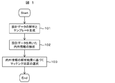
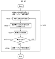
- the flowchart explaining a pattern matching process The figure explaining the outline of the measurement or inspection system which performs pattern matching.
- the flowchart explaining an example of the selection process (step 103) of a matching position The flowchart explaining an example of the selection process (step 103) of a matching position.
- the reflection of the lower layer pattern can be suppressed, but since information other than the edge is excluded, matching is appropriate when the pattern deformation is large. There may be a case where is not performed.
- the correlation value required for the matching calculation may be reduced.
- the lower layer pattern 301 has a shape close to the design data, but the upper layer pattern 302 is deformed.
- a pattern matching method comprising: a step of specifying an image region; a step of calculating a statistic of information based on luminance of the image region; and a step of determining a matching position by comparing the statistic with a threshold value
- a pattern matching method comprising: specifying at least one image region; calculating a profile based on luminance of the image region; and determining a matching position by comparing the shape of the profile with a predetermined profile.
- a method of performing pattern matching between an image taken of an electronic device or the like and a reference pattern formed based on design data the image corresponding to the inside or the outside of the reference pattern is displayed. Identifying at least one or more image regions, calculating a statistic of information based on luminance of the image region, calculating the statistic for at least two candidate points, and A pattern matching method including a step of selecting matching candidates by performing comparison, an apparatus for realizing the pattern matching method, and a computer program will be described in detail.
- a method of performing pattern matching between an image taken of an electronic device or the like and a reference pattern formed based on design data the image corresponding to the inside or the outside of the reference pattern is displayed. Identifying at least one or more image regions, calculating a statistic of information based on luminance of the image region, calculating the statistic for at least two candidate points, and determining the statistic
- a pattern matching method including a step of clustering using threshold comparison and a step of selecting a matching correct candidate from the class obtained by the clustering, an apparatus for realizing the pattern matching method, and a computer program will be described in detail.
- a method of performing pattern matching between an image taken of an electronic device or the like and a reference pattern formed based on design data the image corresponding to the inside or the outside of the reference pattern is displayed. Identifying at least one or more image regions, calculating a statistic of information based on luminance of the image region, calculating the statistic for at least two candidate points, and A pattern matching method including a step of clustering based on comparison and a step of selecting a matching correct candidate from the class obtained by the clustering, an apparatus for realizing the pattern matching method, and a computer program will be described in detail.
- a method of performing pattern matching between an image taken of an electronic device or the like and a reference pattern formed based on design data the image corresponding to the inside or the outside of the reference pattern is displayed.
- a pattern comprising: identifying at least one image area of the image area; calculating a statistic of information based on luminance of the image area; and determining a matching error by comparing the statistic with a threshold value
- a method of performing pattern matching between an image taken of an electronic device or the like and a reference pattern formed based on design data the image corresponding to the inside or the outside of the reference pattern is displayed. Identifying at least one or more image regions, calculating a statistic of information based on luminance of the image region, calculating the statistic for at least two candidate points, and A pattern matching method including a step of determining a matching failure by performing comparison, an apparatus for realizing the pattern matching method, and a computer program will be described in detail.
- a method of performing pattern matching between an image taken of an electronic device or the like and a reference pattern formed based on design data the image corresponding to the inside or the outside of the reference pattern is displayed. Identifying at least one image area, calculating a statistical amount of information based on luminance of the image area, calculating the statistical amount for at least two candidate points, and for the candidate points.
- Pattern matching method, apparatus for realizing the same, and computer program It will be described in detail.
- a method of performing pattern matching between an image taken of an electronic device or the like and a reference pattern formed based on design data the image corresponding to the inside or the outside of the reference pattern is displayed. Identifying at least one or more image regions, calculating a statistic of information based on luminance of the image region, calculating the statistic for at least two candidate points, and A pattern matching method comprising: a step of changing a clustering method; a step of performing clustering using a comparison between the statistic and a threshold value or a statistic; and a step of selecting a matching correct answer candidate from the class obtained by the clustering , Device for realizing this, and computer program in detail Explain.
- a method of performing pattern matching between an image taken of an electronic device or the like and a reference pattern formed based on design data the image corresponding to the inside or the outside of the reference pattern is displayed. Identifying at least one or more image regions, calculating a statistic of information based on luminance of the image region, a comparison result between the statistic and a threshold value or two or more statistic, and an image
- a pattern matching method including a step of specifying a matching position based on a correlation result, an apparatus for realizing the pattern matching method, and a computer program will be described in detail.
- selecting a matching correct candidate from the class an example of selecting one matching candidate from the matching candidates in the class using the result of image correlation will be described.
- the step of selecting a matching correct candidate from within the class will also be described with respect to an example in which one matching candidate is selected from the matching candidates in the class based on the statistics and the result of image correlation.
- a method of performing pattern matching between an image taken of an electronic device or the like and a reference pattern formed based on design data the image corresponding to the inside or the outside of the reference pattern is displayed.
- a pattern matching method including a step of specifying at least one image area and a step of determining a matching position using the image area, an apparatus for realizing the pattern matching method, and a computer program will be described in detail.
- As the step of determining the matching position using the image region a step of performing an image correlation calculation, a step of calculating a statistical amount of information based on the luminance of the image region, or a profile based on the luminance of the image region An example having at least one of the calculating steps will also be described.
- the step of determining a matching position using the image region includes at least one of a value based on an image correlation calculation, a comparison result of a statistic obtained from the image region, and a comparison result of a profile obtained from the image region.
- An example of determining the matching position based on one will also be described.
- a matching position by comparing the shape of the profile with a predetermined profile
- a matching position is determined by comparing the profile given based on an arbitrary profile or design data with the profile. explain.
- the success rate of matching can be improved for complex patterns and multilayer patterns. Moreover, the increase in calculation cost is slight and the time required for re-inspection is greatly reduced, leading to a reduction in the time required for the entire process. In addition, since the matching success rate is improved, the labor of the user is reduced and the operability is improved.
- FIG. 1 is a flowchart illustrating a template creation process and a pattern matching process.
- the pattern matching method described below includes a step of analyzing design data and generating a template (step 101), a step of analyzing internal / external information using design data (step 102), and matching based on an analysis result of internal / external information.
- a step (step 103) of selecting a position is included.
- the pattern matching method in this embodiment can be applied to a system for measuring and inspecting semiconductor devices. For example, in the measurement or inspection process of a semiconductor device, design data and the dimension of a pattern formed on the semiconductor device are measured, a defect is inspected, and the like.
- a template that is applied to pattern matching for specifying a measurement / inspection position is created using design data including a part to be measured or inspected.
- SEM scanning electron microscope
- the present invention can also be applied to search for a desired pattern from an image obtained by another image forming apparatus (for example, a focused ion beam (FIB) apparatus which is a kind of charged particle beam apparatus).
- FIB focused ion beam
- the design data is a semiconductor circuit design drawing.
- the design data is expressed in, for example, the GDS format or the OASIS format, and is stored in a predetermined format.
- the design data can be of any type as long as the software that displays the design data can display the format and can handle the data as graphic data.
- the image processing apparatus described in the present embodiment may be integrated with a control device of an SEM that is a kind of image forming apparatus, or includes a storage medium that stores image signals obtained by the SEM, and the image signal
- a processor that executes a program for executing matching above, or a dedicated processor, may be a separate computer connected to the SEM via a network or the like.
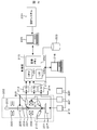
- FIG. 2 is a diagram for explaining an outline of a measurement or inspection system for performing pattern matching.
- the electron optical system 202 is converged with an electron gun 203 that generates an electron beam (primary electron) 204, and a condenser lens (not shown) that converges the electron beam 204 extracted from the electron gun 203 by an extraction electrode 205.
- the semiconductor wafer 201 is placed on the XY stage 217.
- the deflector 206 and the objective lens 208 are arranged such that the electron beam irradiation position and the aperture stop so that the electron beam is focused and irradiated at an arbitrary position on the semiconductor wafer 201 placed on the XY stage 217. And control.
- the XY stage 217 moves the semiconductor wafer 201 so that an image of an arbitrary position of the semiconductor wafer 201 can be taken.
- stage shift changing the observation position by the XY stage 217
- deflecting the electron beam by the deflector 206 changing the observation position by deflecting the electron beam by the deflector 206
- beam shift changing the observation position by deflecting the electron beam by the deflector 206
- secondary electrons and reflected electrons are emitted from the semiconductor wafer 201 irradiated with the electron beam, and the secondary electrons are detected by the secondary electron detector 209.
- the reflected electrons are detected by the reflected electron detectors 210 and 211.
- the backscattered electron detectors 210 and 211 are installed at different positions. Secondary electrons and reflected electrons detected by the secondary electron detector 209 and the reflected electron detectors 210 and 211 are converted into digital signals by the A / D converters 212, 213 and 214, and input to the processing control unit 215.
- the image data is stored in the image memory 252, and the length of the circuit pattern is measured by performing image processing according to the purpose using the CPU 251 or image processing hardware.
- the processing control unit 215 uses the stage controller 219 and the deflection control unit 220 to image the measurement points based on the imaging recipe created by the imaging recipe creation unit 225 described later and indicating the pattern length measurement procedure.
- a control signal is sent, and further, processing and control such as performing various image processing on the observation image on the semiconductor wafer 201 are performed to perform positioning by pattern matching.
- the processing control unit 215 observes a global alignment mark on the semiconductor wafer 201 with an optical microscope (not shown) or the like, thereby including XY including global alignment control for correcting the origin deviation of the semiconductor wafer 201 and the rotation of the wafer.
- the processing control unit 215 has a function such as a GUI (Graphcal User ⁇ ⁇ Interface) that is connected to a display 216 provided with input means and displays an image, a measurement result, and the like to the user.
- GUI Graphcal User ⁇ ⁇ Interface
- the Example provided with the detector of two reflected electron images was shown, it is also possible to increase or decrease the number of the detectors of the said reflected electron image.
- part or all of the control in the processing control unit 215 can be assigned to a CPU or an electronic computer equipped with a memory capable of storing images, and can be processed and controlled.
- the processing control unit 215 further creates an imaging recipe that includes information on the circuit pattern coordinates, positioning design data template corresponding to the coordinates, and imaging conditions (including imaging magnification and image quality) for SEM observation. It is connected to the recipe creation unit 225 via a network or a bus.
- the photography recipe creating unit 225 is connected to a design system 230 such as an EDA (Electrnic Design Automation) tool via a network or the like in order to acquire design data.
- the photographing recipe creation unit 225 creates a photographing recipe using design data from information on photographing points on a wafer to be measured. For example, a photographing recipe disclosed in Japanese Patent Laid-Open No. 2006-3517146 is disclosed. The creation device corresponds to this.
- the concept of creating a shooting recipe from design data has been proposed for a long time, and does not limit the method and apparatus for generating a shooting recipe from design data.
- the creation of a photographing recipe is generally executed by software processing of an electronic computer equipped with a CPU, memory, etc., and hardware processing equipped with a CPU, ASIC, FPGA, memory, etc.
- an exposure simulator may be connected to the imaging recipe creation unit 225 so that line segment information indicating the outline of the pattern is read by the imaging recipe creation unit 225.
- the matching position is determined by selectively extracting information on the inside and / or outside of the pattern and evaluating the feature amount.
- the line segment of the layout data of the pattern included in the GDS data indicates the ideal shape of the pattern, but the actually formed pattern does not necessarily match the layout data. Therefore, by defining the pattern line segment based on the simulation having a shape closer to the shape of the actual pattern as the boundary line inside and / or outside the pattern, the matching accuracy can be further improved. Simulation data is also formed based on the design data.
- FIG. 5 is a diagram for explaining an example of setting the optical condition adjustment area, measurement, and inspection point on the layout data.
- AP addressing point
- SP stigma correction point
- BP brightness and contrast adjustment point
- the imaging location and imaging conditions (including imaging magnification and image quality) in the imaging sequence, and the length measurement conditions in the EP are created by the imaging recipe creation unit 225 as an imaging recipe based on the design data and information on the length measurement points. It is stored and managed in the storage device 223.
- the semiconductor wafer 201 is mounted on the XY stage 217 (step 2001).
- the processing control unit 215 calculates the origin deviation and rotation deviation of the sample, and the stage controller 219 is controlled based on these deviation amounts.
- the coordinate deviation of the sample is corrected (step 2002).
- the process control unit 215 moves the XY stage 217 to move the imaging position to the AP in accordance with the coordinates of the imaging point created by the imaging recipe creation unit 225 and the imaging conditions, so that it is lower than that at the time of EP imaging.
- the imaging is performed under the imaging conditions (step 2003).
- the processing control unit 215 controls the deflector 206 via the deflection control unit 220 by the amount obtained by subtracting the detected deviation vector from the relative vector between the coordinates of the design data template and the coordinates of the EP.
- the beam is shifted (the irradiation position is changed by tilting the incident direction of the beam), and the imaging position is moved to acquire the EP image.
- the positioning accuracy of the beam shift is higher than the positioning accuracy of the stage, the positioning can be performed with high accuracy. As described above, by providing the AP, high-precision positioning is possible regardless of the stage positioning accuracy and the like.
- the imaging position is moved to the FP by beam shift, the FP is imaged to obtain an autofocus parameter, and the autofocus is performed based on the obtained parameter. Perform (step 2004).
- the imaging position is moved to the SP by beam shift and imaging is performed to obtain astigmatism correction parameters, and automatic astigmatism is calculated based on the obtained parameters.
- Correction auto stigma correction
- the imaging position is moved to the BP by beam shift and imaging is performed to obtain parameters for brightness & contrast adjustment.
- automatic brightness & contrast is obtained. Adjustment is performed (step 2006).
- steps 2003, 2004, 2005, and 2006 described above may be partially or completely omitted depending on circumstances. It is also possible to change the order of steps 2003, 2004, 2005, and 2006, or to overlap the coordinates (for example, autofocus and autostigma are performed at the same location).
- the imaging position is moved to the EP by beam shift, and imaging is performed.
- the design data template in the EP registered in the storage device 223 and the SEM image of the observed EP are Matching is performed to calculate the shift amount of the length measurement point in the SEM image (step 2007).
- the length measurement is performed on the length measurement points on the design data given by the imaging recipe.
- FIG. 6 is an image diagram of design data.
- the design data is generally designed by an EDA tool and has vector information, image information, text information, or combination information of these information.
- the circuit diagram of the semiconductor device is written in the design data.
- Information corresponding to one circuit on a semiconductor is collectively referred to as one line.
- the design data has circuit information of at least one line.
- Some circuit diagrams written in the design data have a multilayer structure, and each layer is referred to as a layer here.
- the design data is given in a format that allows the layer to be identified, what hits the upper layer is called the upper layer 601, and what is written in the lower part of the upper layer is called the lower layer 602.
- Each layer has circuit edge 603 information and inside / outside information indicating whether it is inside a closed figure (604, 605) or outside 606 of a closed figure.
- a matching method for setting a matching area will be described based on information on an area divided by a closed figure or a line segment forming a pattern.
- the internal / external information and the information related to the area may be the same.
- the inside / outside information can be represented by the drawing direction of a closed figure if it is vector data, and the brightness of the cell if it is image data.
- the specification of the design data varies depending on the design method, and does not necessarily match the layout characteristics illustrated in FIG.
- design data there may be more than one layer in the design data.
- the embodiment described below is effective regardless of the format of the design data.
- mask data with OPC Optical Proximity Correction
- process data required for the manufacturing process can be handled as design data.
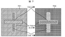
- FIG. 7 schematically shows the characteristics of a circuit pattern image (hereinafter referred to as an SEM image) taken using an SEM. Comparing the right and left figures in FIG. 7, even if the SEM images have the same pattern, the luminance may change due to various factors such as changes in process conditions and changes in optical conditions of the electron microscope. For example, the contrast is reversed between the portion 701 and the portion 702 that are background portions with respect to the pattern, although they are in the same place.
- the edge portion 703 of the SEM image generally has high brightness due to the influence of the edge effect.
- This part is usually called a white band.
- the length and width of white bunts formed on the basis of the above principles vary depending on design data and workmanship.
- the area other than the white band, the area surrounded by the white band, or the area outside the area is affected by noise, but the luminance change in the area is small (flat). have. More specifically, the change in luminance within the pattern or within the external region is relatively small compared to a region including a plurality of different members or a region including an edge portion.
- two or more layers may be displayed in the SEM image.
- a pattern in the uppermost layer (a pattern not hidden in other patterns on the SEM image) is defined as an upper layer 704.
- a pattern (a lower layer 705) that partially overlaps the pattern of the upper layer 704 and is arranged in a lower layer of the upper layer 704 does not display the superimposed portion on the SEM image.
- a recent semiconductor device has a multi-layer structure, and a pattern may exist in a lower layer of a lower layer pattern (lower layer 705). Even when the lower layer patterns overlap with each other in this way, a part of the lower layer side pattern is not displayed in the SEM image.
- the pattern feature area of the pattern internal area (hereinafter referred to as the pattern inside), the pattern external area (hereinafter referred to as the pattern external area), and the edge portion, which can be specified by associating the SEM image with the design data, is different.
- a method of performing pattern matching based on the difference in feature amount between the two or more regions will be described.
- a matching method for a pattern composed of two layers of an upper layer pattern and a lower layer pattern will be mainly described.
- the matching method in this embodiment can be applied if a pattern of a single layer (one layer) or more exists. is there.
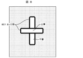
- a design data template (hereinafter referred to as a template) is created by performing a process for giving a width to the edge portion 801 from the design data illustrated in FIG. 8, and is used as a template for matching with an SEM image having a white band. Conceivable. Since the white band has a certain width, it is possible to suppress the deviation of the feature amount between the SEM image and the design data by performing the above processing.
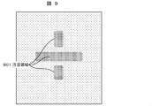
- a region corresponding to the edge portion is excluded from the design data, and an internal region of the pattern is extracted.
- the extracted area is set as an attention area 901.
- a portion corresponding to the inside of the pattern in the design data is defined as an internal region
- a portion corresponding to the outside is defined as an external region.
- Extraction of the region of interest can be obtained from design data using manual or automatic analysis.
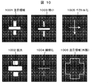
- the region of interest is a line or surface written on the image, and its shape is variable depending on a parameter used as an index for pattern matching.
- an enlarged pattern 1002 is formed, a reduction process is performed, a reduced pattern 1003 is formed, and a thinning process is performed.
- a thin line 1004 form vector data 1005 by vectorization processing, and the like.
- These areas can also be defined as attention areas.
- an external attention area 1006 can be formed by performing the above processing on the external area. Thereafter, when acquiring the inside / outside information, if there is no premise, all the information is acquired from the attention area.
- the attention area illustrated in FIGS. 9 and 10 includes a multilayer pattern, and the lower attention area is partially hidden in the upper layer.
- the upper and lower attention areas can be obtained independently. In that case, it acquires with the shape except the edge part and internal area
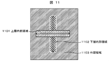
- FIG. 11 shows the inside and outside areas of the pattern of the SEM image.
- the definitions of the upper layer internal area 1101, the lower layer internal area 1102, and the external area 1103 correspond to the upper layer internal 604, lower layer internal 605, and external 606 of the corresponding design data, respectively. These definitions vary depending on how design data is given.
- the step of acquiring the information on the attention area is included in the design data analysis and template generation 101.
- the execution order is not limited, and any steps may be performed before and after.
- an index value of the region is selectively obtained, and a matching position is specified based on the index value.
- the matching position is specified based on a determination as to whether an index value unique to a certain region of interest satisfies a predetermined condition. For example, at the time of matching, the template and the SEM image are overlapped to obtain at least one piece of information such as the brightness of each pixel in the region of interest and the surrounding inclination. Let the information obtained as an example be luminance.
- index values For the acquired luminance information, one or more parameters (hereinafter referred to as index values) such as maximum value, minimum value, average value, standard deviation, variance, differential value around the pixel, number of luminance peaks, luminance waveform of the region of interest, etc. ). Based on the calculation result, matching is executed.
- index values such as maximum value, minimum value, average value, standard deviation, variance, differential value around the pixel, number of luminance peaks, luminance waveform of the region of interest, etc.
- the embodiment will be described using the maximum value, minimum value, average value, standard deviation, variance, etc. as statistics, the number of luminance peaks, luminance waveform, etc. as analysis results. Note that it is desirable to arbitrarily select the index value according to the feature of the attention area. Further, the parameters included in the statistics and profile are not limited to the above examples.
- the step of acquiring at least one piece of information such as the luminance of each pixel in the region of interest and the surrounding inclination is included in the analysis 102 of inside / outside information using design data.
- the execution order is not limited, and step 101 may be performed before.
- a step of generating a template and a region of interest from design data (step 101), and a step of acquiring and analyzing the brightness of the SEM image superimposed on the region of interest at an arbitrary position (analysis of internal information) Step: Step 102) is executed, and then a matching position is selected based on the analysis result of the internal information (Step 103), from the template creation in this embodiment to the matching by the created template.
- Step 103 the following processing is specifically performed.
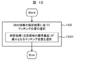
- FIG. 12 is a flowchart for explaining an example of the matching position selection step (step 103).
- the matching position is specified by selecting the position where the analysis result (for example, the standard deviation of the luminance value of the attention area) is minimized.
- the standard deviation of the luminance of the attention area is calculated.
- the standard deviation is assumed to be an index value I.
- the threshold value is set to zero because the change in luminance tends to be flat.
- a matching position where the index value I is closest to the threshold value is acquired and set as a matching correct position.
- the threshold value is an arbitrarily given value, and the index value I is not limited to the standard deviation.
- a process may be included such as filtering the SEM image to sufficiently reduce the influence of noise.
- accurate matching can be performed according to the feature quantity inside or outside the pattern.
- the analysis in the searched area on the SEM image is performed on the attention area by using the template having the index value I information as described above, for example, both the pattern edge and the line segment of the lower pattern, and the inside of the pattern.
- the edge portion and the like have higher brightness than the inside of the pattern, and therefore the brightness varies in the attention area.
- the attention area and the pattern internal area coincide with each other, as described above, the change in luminance is small within the pattern, and thus the standard deviation is close to zero.
- This example can increase the success rate of matching when pattern edges and the like are mixed in addition to the matching position and there is no shape-unique portion.
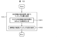
- FIG. 13 is a flowchart for explaining another example of the matching position selection step (step 103).
- the matching position is selected using both the matching score and the internal information analysis result.
- a step (Step 1301) of generating an index value I using the score F at each matching position obtained by performing the image correlation calculation and a statistic in the internal analysis result of the region of interest and the index value A step (step 1302) of selecting a matching position where I is optimal.
- the statistic is the standard deviation S. As described above, except for the edge portion of the SEM image, the luminance change is flat except for noise. If the matching based on the correlation value calculation is successful, the ideal value of S is zero.
- the matching position where the index value I is maximized is set as the matching correct position.
- Such a calculation method of the index value I is not limited to the above calculation formula.
- FIG. 14 is a flowchart for explaining still another example of the matching position selection step (step 103).
- a candidate point is selected by determination using a matching score, and an optimal matching position is selected for the candidate point using a statistic or the like.
- a step (step 1401) of acquiring one or more candidate points satisfying an arbitrary threshold value in order from a matching position with a high score F, and acquisition A step (step 1402) of selecting an optimal matching position from the statistics obtained as the inside / outside information for one or more candidate points is included.
- the threshold value may be 80% of the maximum score. That is, a part having a score equal to or higher than a predetermined value is defined as a candidate point.
- a matching position M satisfying M ⁇ 0.8F is set as a candidate point for the matching position M.
- the final matching position is narrowed down by determining a region of interest using the statistics for the candidate points extracted in this way.
- the statistic is the standard deviation S of luminance. For these candidate points, the standard deviation of luminance is compared under the assumption that the luminance change in the region of interest is flat, and the candidate with the smallest standard deviation is set as the matching position.
- the threshold value is arbitrarily determined, and the method for selecting candidate points is not limited to the condition that the score is 80% or more.
- the standard deviation of luminance is one of general examples of statistics, and is not limited to this.
- the clustering method is not limited to the above. For example, a known clustering method such as the k-means method or the shortest distance method may be used. In addition, a clustering method that relatively compares feature quantities of candidate points may be used.
- the first matching method based on image correlation or the like and the second matching method based on the feature amount determination of the attention area described above are used in combination. Accurate matching can be performed. In particular, one matching method can narrow down the choices of the other matching candidate, which is effective in suppressing matching errors.
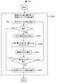
- the flowchart of FIG. 15 includes a step of determining whether or not clustering of matching candidates is necessary (step 1501), a step of selecting a clustering method from the statistics when executing clustering (step 1502), and the use of statistics. Performing clustering (step 1503), selecting an optimal class from the clustering result (step 1504), selecting whether further clustering is to be performed within the optimal class (step 1505), and from within the class The step of selecting a matching position (step 1506) is included.
- Step 1501 is a step of determining that there is no need for clustering if, for example, all candidate points are within ⁇ 10% of the average value of statistics. This is a step of determining whether the matching position should be obtained by clustering of candidate points when it is considered that clustering cannot be performed well due to the influence of noise or the like when the statistic variation is small.
- the determination method in step 1501 may be arbitrarily set. Alternatively, it may be automatically set from a statistic or the like.
- Step 1502 is a step of determining a statistic and a clustering method as an index. For example, if the index value is the standard deviation, select the clustering method using the average value of the standard deviation or the clustering method based on whether the standard deviation is closer to the maximum value or the minimum value. It is a technique. If it can be determined in step 1501 that the maximum value and the minimum value are sufficiently separated from each other, the clustering is selected depending on which of the standard deviation is closer to the maximum value or the minimum value. Further, this is a step of selecting a clustering method in accordance with the statistics to be used.
- Step 1503 is a step of clustering candidate points into two depending on whether the standard deviation is closer to the maximum value or the minimum value, for example.
- Step 1504 uses, for example, the feature that the standard deviation is small when the region of interest is in the upper layer, and based on the result obtained in Step 1504, the candidate point class close to the minimum value is the optimal candidate It is a step to make a class.
- Step 1505 is a step for selecting whether to perform clustering again. For example, the standard deviation is examined in the candidate point class close to the minimum value, and if the difference between the maximum and minimum standard deviations in the class is larger than an arbitrary value, clustering is performed again. If the maximum and minimum difference is smaller than an arbitrary value, clustering is not performed again. This is a step of determining which of the two processes is executed.
- Step 1506 is a step in which, for example, the candidate having the maximum score in the class is set as the matching position. Any clustering method, clustering execution determination method, and index value may be used.
- FIG. 21 is a flowchart for explaining a process of selecting an optimum matching position using a statistic from candidate points without performing the clustering execution determination step (step 1501) in FIG.
- step 2101 for determining whether to perform reclassification.
- reclassification execution determination is performed. For example, since the step from step 1502 to step 2101 is performed n times, it is a step of determining the current number of times.
- n has a value from 0 to the number of candidate points.
- matching candidates before clustering are output to step 1506.
- the number n of re-clustering may be specified by a human or may be automatically calculated from some feature of the candidate point group.
- the reclassification execution determination in step 2101 may determine the validity of the clustering result. For example, a class before classification and a class group after classification are mutually or absolutely compared using a statistic criterion, an information criterion, a histogram, a threshold value, and the like. For example, a Bayes information criterion that is a known technique is used as a method for determining the validity of the clustering result. If the classification is valid, reclassify the optimal class. If the classification is not valid, the class before classification is output to step 1506. Any reclassification execution determination method other than the above may be used.
- the pattern matching method described in detail above can be installed as a computer program for operating a dedicated image processing processor or a general-purpose arithmetic processor in the electron microscope or image processing apparatus having the image processing function shown in FIG.
- a dedicated image processing processor or a general-purpose arithmetic processor in the electron microscope or image processing apparatus having the image processing function shown in FIG.
- the template and the SEM image can be matched at high speed.
- the matching success rate can be improved by combining with the image correlation calculation.
- the information required for matching can be obtained from the design data and the SEM image, the burden on the user can be reduced.
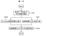
- FIG. 16 is a flowchart for explaining an example of the matching error determination method. After step 102 illustrated in FIG. 1 is executed, a step of comparing an analysis result with a threshold (step 1601), or two or more analysis results are displayed. A step of comparing (step 1602) and a step of determining a matching failure from the comparison result (step 1603) are executed.
- Steps 1601, 1602, and 1603 will be described in detail. It is assumed that the analysis result obtained in step 102 is given as a statistic, and here is the standard deviation S. If matching is successful, the ideal value of S is zero. In step 1601, the standard deviation S is compared with an arbitrarily given threshold value. If the standard deviation S is larger than the threshold value, it is determined in step 1603 that the matching has failed. In step 1602, the magnitude of two or more standard deviations S1 and S2 is obtained. At this time, the larger one is determined as a matching failure in step 1603. Each of the above parameters can be set to an arbitrary value.
- the matching error determination method as described above can be mounted on an electron microscope having an image processing function as illustrated in FIG. 2 or an image processing apparatus, and includes pattern inside / outside information (for example, upper layer internal 604, lower layer internal 605). By using the external 606), a matching failure can be determined. As a result, when performing pattern matching, it is not necessary to perform matching processing at an incorrect answer position, so that high-speed processing is possible. In addition, since the incorrect answer positions are removed in advance, the matching success rate can be increased. In addition, since the number of images to be determined when the user determines the matching success position can be reduced, the burden on the user can be reduced.
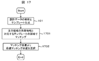
- FIG. 17 is a flowchart for explaining an example of a matching method that selectively uses a region of interest. After executing step 101 illustrated in FIG. 1, an arbitrary image region corresponding to the region of interest corresponds to the region of interest. A step of matching using a region on the template (step 1701) and a step of selecting an optimum matching position from the matching result (step 1702) are executed.
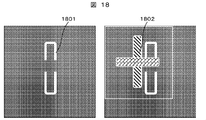
- FIG. 18 is a diagram illustrating a specific example of a matching method using a template that selectively uses a region of interest.
- the SEM image and the design data have a multilayer structure, and the region of interest is outside the upper layer.
- matching is performed using a lower layer template 1801 (hereinafter referred to as a difference template) that masks the region of interest (upper layer portion) of the template.
- the left diagram in FIG. 18 is a diagram for explaining an example of the difference template, and the right diagram is a diagram for explaining an execution example of the matching using the difference template on the SEM image 1802.
- the method of the embodiment described so far can be applied.
- the above method can be used as a region of interest regardless of a single layer or a multilayer.
- the pattern matching method as described above can be installed in an electron microscope having an image processing function as illustrated in FIG. 2 or an image processing apparatus, and the inside / outside information of the pattern (for example, upper layer interior 604, lower layer interior 605). , External 606) can be selectively used to perform template and SEM image matching at high speed. Furthermore, since the information required for matching can be obtained from the design data and the SEM image, the burden on the user can be reduced.
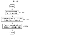
- FIG. 19 is a flowchart for explaining an example of a matching method used for profile information of a region of interest.
- a profile obtained from the region of interest at an arbitrary position using a profile as an index after executing step 101 illustrated in FIG. And a step of comparing an arbitrary profile (step 1901) and a step of selecting an optimal matching position based on the profile comparison result (step 1902).
- the profile mentioned here is an ideal profile in a region of interest set by the user or a profile based on a template.
- step 1901 for example, a differential filter is applied to the profile obtained from the region of interest to detect the number of peaks higher than the average value of luminance.
- the number of detected peaks is compared with the number of peaks in the profile based on the template.
- processing such as normalization correlation with the profile obtained from the template for the profile subjected to the differential filter.
- Step 1902 selects an optimal matching position based on the comparison result.
- Clustering based on coincidence / inconsistency of the number of peaks, clustering based on comparison between peaks, or the like may be performed by the above comparison. From the above comparison results, the candidate point whose peak shape is closest to the ideal value, or the candidate point with the highest image correlation score after clustering is selected as the best matching candidate.
- parameters that are replaced as statistics of the execution example such as the number of peaks, can be adapted to the execution example.
- the pattern matching method as described above can be installed in an electron microscope or an image processing apparatus having an image processing function as illustrated in FIG.
- the template and the SEM image can be matched at high speed.
- pattern matching can be performed for a region of interest in which other layers are reflected in the multilayer image, and the matching success rate can be improved.
- the information necessary for the matching can be obtained from the design data and the SEM image, the burden on the user can be reduced.
- the image processing apparatus for the above embodiment.
- it can be executed by an image processing apparatus mounted on a CD-SEM (Critical Dimension-SEM) or a personal computer that executes a program for pattern matching.
- these apparatuses may be provided with a function for the user to arbitrarily set execution non-execution for the processing of the above-described embodiment, or a user interface for setting to selectively execute some functions.
- the pattern matching method described so far can be installed in an electron microscope having an image processing function as illustrated in FIG. 2 or an image processing apparatus, and the execution mode can be changed according to conditions desired by the user. Therefore, the processing time and success rate can be adjusted to the user's needs.
- the SEM is used to obtain an image of the semiconductor device.
- the above-described method may be applied to pattern matching using an image acquired using an imaging device other than the SEM. Is possible. For example, it is possible to obtain an equivalent action and effect even by using an apparatus that obtains an image of a semiconductor device using an optical photographing means, but scanning electrons that form an image with more noise than an optical microscope or the like. By applying to a charged particle beam apparatus such as a microscope, a higher effect is exhibited.
Landscapes
- Engineering & Computer Science (AREA)
- Physics & Mathematics (AREA)
- Theoretical Computer Science (AREA)
- General Physics & Mathematics (AREA)
- Computer Vision & Pattern Recognition (AREA)
- Data Mining & Analysis (AREA)
- Multimedia (AREA)
- Evolutionary Computation (AREA)
- Artificial Intelligence (AREA)
- Software Systems (AREA)
- Probability & Statistics with Applications (AREA)
- Evolutionary Biology (AREA)
- Bioinformatics & Computational Biology (AREA)
- Bioinformatics & Cheminformatics (AREA)
- Life Sciences & Earth Sciences (AREA)
- General Engineering & Computer Science (AREA)
- Electromagnetism (AREA)
- Quality & Reliability (AREA)
- Analytical Chemistry (AREA)
- Chemical & Material Sciences (AREA)
- Computing Systems (AREA)
- Health & Medical Sciences (AREA)
- Medical Informatics (AREA)
- Databases & Information Systems (AREA)
- General Health & Medical Sciences (AREA)
- Image Analysis (AREA)
- Testing Or Measuring Of Semiconductors Or The Like (AREA)
- Analysing Materials By The Use Of Radiation (AREA)
- Image Processing (AREA)
- Length Measuring Devices By Optical Means (AREA)
Abstract
In order to provide a computer program, an image processing device, and a pattern matching method that perform pattern matching at a high level of accuracy without relying on edge deformation, contrast fluctuations, etc., in one embodiment, the disclosed pattern matching method and device perform pattern matching over an image using a template produced on the basis of the belowmentioned design data. The pattern matching method and device determine the characteristic quantities of the image for an inner region and/or an outer region that are divided by a line that defines the contour of a pattern, and determine positions at which said characteristic quantities satisfy predetermined conditions to be matching positions, matching position candidates, or erroneous matching positions.
Description
本発明は走査電子顕微鏡等によって得られた画像信号を処理する画像処理装置に係り、特に画像上でのテンプレートマッチング方法、それを実現する画像処理装置、及びコンピュータプログラムに関する。
The present invention relates to an image processing apparatus that processes an image signal obtained by a scanning electron microscope or the like, and more particularly, to a template matching method on an image, an image processing apparatus that realizes the same, and a computer program.
従来から、対象画像において与えられた特定の形状(テンプレート)を探索する技術はテンプレートマッチングとして広く用いられている。
Conventionally, a technique for searching for a specific shape (template) given in a target image has been widely used as template matching.
走査式電子顕微鏡を用いた半導体ウェハ上のパターンの計測においても、計測位置を求めるためにテンプレートマッチングが行われている。(特許文献1参照)計測位置の大まかな位置合わせはウェハを載せたステージの移動によって行われるが、ステージの位置決め精度では電子顕微鏡の高い倍率で撮影された画像上で大きなズレが生じる。このズレを補正して正確な位置での計測を行うためにテンプレートマッチングが行われる。
In template measurement on a semiconductor wafer using a scanning electron microscope, template matching is performed in order to obtain a measurement position. (Refer to Patent Document 1) Rough positioning of the measurement position is performed by moving the stage on which the wafer is placed. However, with the positioning accuracy of the stage, a large deviation occurs on an image photographed at a high magnification of an electron microscope. Template matching is performed in order to correct this shift and perform measurement at an accurate position.
しかし、予期しない下層パターンの写り込みにより、正しくマッチングが行われず、正しいマッチング位置を得ることができない場合がある。そのため、設計データのエッジのみを用いてマッチング処理を行う方式(特許文献2参照)が提案されている。この方法は設計データから得たエッジのみでマッチングを行い、その他の領域では相関演算を無視することで、下層パターンの写り込みによる相関値の低下を抑制することができる。
However, due to unexpected reflection of the lower layer pattern, matching may not be performed correctly, and the correct matching position may not be obtained. For this reason, a method of performing matching processing using only the edges of design data (see Patent Document 2) has been proposed. In this method, matching is performed only with edges obtained from design data, and correlation calculation is ignored in other regions, so that a decrease in correlation value due to reflection of a lower layer pattern can be suppressed.
しかしながら、特許文献2に説明されているようなマッチング法では、エッジ部分の情報のみを用いてマッチングを行っているため、例えばライン幅とスペース幅が同じ間隔で多数配列されているようなパターン(ラインアンドスペースパターン)の場合、半周期ずれた位置をマッチング位置であるとして誤認識する可能性がある。このようにパターンの種類によっては、エッジ以外の領域も利用することによって、マッチング処理を行った方がマッチングの精度を高められるものもある。更に、プロセス変動等の要因により、パターン幅が設計データと大きく異なるような場合、マッチングの精度が低下する可能性もある。
However, in the matching method as described in Patent Document 2, since matching is performed using only the information on the edge portion, for example, a pattern in which a large number of line widths and space widths are arranged at the same interval ( In the case of a line and space pattern, there is a possibility that a position shifted by a half cycle is erroneously recognized as a matching position. As described above, depending on the type of pattern, there is a case where matching accuracy is improved by performing the matching process by using a region other than the edge. Furthermore, if the pattern width is significantly different from the design data due to factors such as process variations, the matching accuracy may be reduced.
以下に、エッジの変形、或いはコントラストの変動等に依らず、高精度にパターンマッチングを行うことを目的とするパターンマッチング方法,画像処理装置、及びコンピュータプログラムについて説明する。
Hereinafter, a pattern matching method, an image processing apparatus, and a computer program for performing pattern matching with high accuracy regardless of edge deformation or contrast fluctuation will be described.
上記目的を達成するための一態様として、以下に設計データに基づいて形成されたテンプレートを用いて、画像上でパターンマッチングを実行するパターンマッチング方法、或いは装置であって、パターンの輪郭を定義する線分によって、区分けされる内側領域、及び/又は外側領域について、画像の特徴量を求め、当該特徴量が所定の条件を満たした位置をマッチング位置,マッチング位置候補、或いは誤ったマッチング位置と決定するパターンマッチング方法,装置、及びコンピュータプログラムを提案する。所定の条件とは例えば、上記領域の輝度のばらつきを示すパラメータである。例えばばらつきが他の部分に対して相対的に小さい、或いは無いと判断できる領域があれば、当該判断に基づいて、マッチング位置を特定する。
As one aspect for achieving the above object, a pattern matching method or apparatus for performing pattern matching on an image using a template formed based on design data below, in which a pattern outline is defined For the inner area and / or outer area, which are classified by line segments, the image feature amount is obtained, and the position where the feature amount satisfies a predetermined condition is determined as a matching position, a matching position candidate, or an incorrect matching position. A pattern matching method, apparatus, and computer program are proposed. The predetermined condition is, for example, a parameter indicating the luminance variation in the area. For example, if there is an area where it can be determined that the variation is relatively small or absent relative to other portions, the matching position is specified based on the determination.
上記構成によれば、エッジの変形、或いはコントラストの変動等に依らず、高精度にパターンマッチングを行うことが可能となる。
According to the above configuration, it is possible to perform pattern matching with high accuracy irrespective of edge deformation or contrast fluctuation.
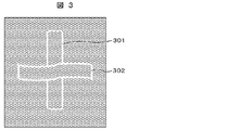
例えば、エッジ部分を選択的に用いてパターンマッチングを行うと、下層パターンの写り込みを抑制することはできるが、エッジ以外の情報を除外しているため、パターンの変形が大きい場合、適正にマッチングが行われないケースが考えられる。図3に例示するように、SEM像上、マッチングの対象となるパターンの一部が崩れているような場合、マッチング演算に要する相関値が低下する可能性がある。図3の例では、下層パターン301は設計データに近い形状を有しているが、上層パターン302は変形している。
For example, if pattern matching is performed by selectively using the edge part, the reflection of the lower layer pattern can be suppressed, but since information other than the edge is excluded, matching is appropriate when the pattern deformation is large. There may be a case where is not performed. As illustrated in FIG. 3, when a part of the pattern to be matched is broken on the SEM image, the correlation value required for the matching calculation may be reduced. In the example of FIG. 3, the lower layer pattern 301 has a shape close to the design data, but the upper layer pattern 302 is deformed.
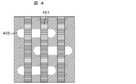
また、図4に例示するように、相対的に縦(Y方向)に長いパターン401と、横(X方向)に長いパターン402が重なり、且つこれらパターンが、パターンの幅と同じ周期で繰り返して存在する場合、エッジ部分を選択的に用いてパターンマッチングを行うと、半周期ずれた位置でも同じエッジの形状であるため、本来のマッチング位置からずれた位置をマッチング位置と認識する可能性がある。半導体パターンでは縦線または横線等の単調の繰り返しパターンは多く用いられ、さらにパターン301と302、及びパターン401と402のように、SEM像にいくつかの層が写り込んでいるような場合には、これらの影響の相乗効果によってマッチング成功率が低下する。
Also, as illustrated in FIG. 4, a pattern 401 that is relatively long in the vertical direction (Y direction) and a pattern 402 that is long in the horizontal direction (X direction) overlap, and these patterns are repeated at the same cycle as the width of the pattern. If it exists, if pattern matching is performed by selectively using the edge portion, the same edge shape is obtained even at a position shifted by a half cycle, and therefore a position shifted from the original matching position may be recognized as a matching position. . In a semiconductor pattern, a monotonous repetitive pattern such as a vertical line or a horizontal line is often used. Further, in the case where several layers are reflected in an SEM image, such as patterns 301 and 302 and patterns 401 and 402. The matching success rate decreases due to the synergistic effect of these influences.
また、近年、半導体デバイスパターンは複雑化と多層化が進み、パターンの歪みや崩れ等の形状変形に基づく影響も大きなものとなっており、マッチング精度を低下させる要因となっている。このようなマッチング精度の低下に対し、テンプレートの形状変形やエッジ強弱をシミュレーションやユーザーが手動で設定しマッチング成功率の向上を行うことが考えられるが、計算コストの増加やマンパワーの不足が懸念される。
Also, in recent years, semiconductor device patterns have become more complex and multilayered, and the influence based on shape deformation such as distortion and collapse of the pattern has become large, which is a factor that lowers matching accuracy. In response to such a decrease in matching accuracy, it is conceivable that the template deformation and edge strength are manually set by the user or simulation to improve the matching success rate. However, there is a concern that the calculation cost will increase and manpower will be insufficient. The
以下に、電子デバイス等を撮影した画像と、設計データに基づいて形成された基準パターンとの間でパターンマッチングを行う手法において、基準パターンの内部または外部に対応する前記画像上の少なくとも1つ以上の画像領域を特定するステップと、前記画像領域の輝度に基づく情報の統計量を算出するステップと、前記統計量としきい値を比較してマッチング位置を決定するステップを有するパターンマッチング法、これを実現する装置、及びコンピュータプログラムを詳細に説明する。
Hereinafter, in a method of performing pattern matching between an image obtained by photographing an electronic device or the like and a reference pattern formed based on design data, at least one or more on the image corresponding to the inside or outside of the reference pattern A pattern matching method comprising: a step of specifying an image region; a step of calculating a statistic of information based on luminance of the image region; and a step of determining a matching position by comparing the statistic with a threshold value, An apparatus to be realized and a computer program will be described in detail.
また、他の態様として、電子デバイス等を撮影した画像と、設計データに基づいて形成された基準パターンとの間でパターンマッチングを行う手法において、基準パターンの内部または外部に対応する前記画像上の少なくとも1つ以上の画像領域を特定するステップと、前記画像領域の輝度に基づくプロファイルを算出するステップと、前記プロファイルの形状と所定のプロファイルを比較してマッチング位置を決定するステップを有するパターンマッチング法、これを実現する装置、及びコンピュータプログラムを詳細に説明する。
As another aspect, in a method of performing pattern matching between an image obtained by photographing an electronic device or the like and a reference pattern formed based on design data, the image corresponding to the inside or outside of the reference pattern is displayed on the image. A pattern matching method comprising: specifying at least one image region; calculating a profile based on luminance of the image region; and determining a matching position by comparing the shape of the profile with a predetermined profile. An apparatus for realizing this and a computer program will be described in detail.
また、更に他の態様として、電子デバイス等を撮影した画像と、設計データに基づいて形成された基準パターンとの間でパターンマッチングを行う手法において、基準パターンの内部または外部に対応する前記画像上の少なくとも1つ以上の画像領域を特定するステップと、前記画像領域の輝度に基づく情報の統計量を算出するステップと、前記統計量を少なくとも2つ以上の候補点について算出し、前記統計量の比較を行うことでマッチング候補を選択するステップを有するパターンマッチング法、これを実現する装置、及びコンピュータプログラムを詳細に説明する。
In still another aspect, in a method of performing pattern matching between an image taken of an electronic device or the like and a reference pattern formed based on design data, the image corresponding to the inside or the outside of the reference pattern is displayed. Identifying at least one or more image regions, calculating a statistic of information based on luminance of the image region, calculating the statistic for at least two candidate points, and A pattern matching method including a step of selecting matching candidates by performing comparison, an apparatus for realizing the pattern matching method, and a computer program will be described in detail.
また、更に他の態様として、電子デバイス等を撮影した画像と、設計データに基づいて形成された基準パターンとの間でパターンマッチングを行う手法において、基準パターンの内部または外部に対応する前記画像上の少なくとも1つ以上の画像領域を特定するステップと、前記画像領域の輝度に基づく情報の統計量を算出するステップと、前記統計量を少なくとも2つ以上の候補点について算出し、前記統計量としきい値の比較を用いてクラスタリングするステップと、前記クラスタリングによって得られたクラス内からマッチング正解候補を選択するステップを有するパターンマッチング法、これを実現する装置、及びコンピュータプログラムを詳細に説明する。
In still another aspect, in a method of performing pattern matching between an image taken of an electronic device or the like and a reference pattern formed based on design data, the image corresponding to the inside or the outside of the reference pattern is displayed. Identifying at least one or more image regions, calculating a statistic of information based on luminance of the image region, calculating the statistic for at least two candidate points, and determining the statistic A pattern matching method including a step of clustering using threshold comparison and a step of selecting a matching correct candidate from the class obtained by the clustering, an apparatus for realizing the pattern matching method, and a computer program will be described in detail.
また、更に他の態様として、電子デバイス等を撮影した画像と、設計データに基づいて形成された基準パターンとの間でパターンマッチングを行う手法において、基準パターンの内部または外部に対応する前記画像上の少なくとも1つ以上の画像領域を特定するステップと、前記画像領域の輝度に基づく情報の統計量を算出するステップと、前記統計量を少なくとも2つ以上の候補点について算出し、前記統計量の比較に基づいてクラスタリングするステップと、前記クラスタリングによって得られたクラス内からマッチング正解候補を選択するステップを有するパターンマッチング法、これを実現する装置、及びコンピュータプログラムを詳細に説明する。
In still another aspect, in a method of performing pattern matching between an image taken of an electronic device or the like and a reference pattern formed based on design data, the image corresponding to the inside or the outside of the reference pattern is displayed. Identifying at least one or more image regions, calculating a statistic of information based on luminance of the image region, calculating the statistic for at least two candidate points, and A pattern matching method including a step of clustering based on comparison and a step of selecting a matching correct candidate from the class obtained by the clustering, an apparatus for realizing the pattern matching method, and a computer program will be described in detail.
また、更に他の態様として、電子デバイス等を撮影した画像と、設計データに基づいて形成された基準パターンとの間でパターンマッチングを行う手法において、基準パターンの内部または外部に対応する前記画像上の少なくとも1つ以上の画像領域を特定するステップと、前記画像領域の輝度に基づく情報の統計量を算出するステップと、前記統計量としきい値の比較によってマッチングの誤りを判定するステップを有するパターンマッチング法、これを実現する装置、及びコンピュータプログラムを詳細に説明する。
In still another aspect, in a method of performing pattern matching between an image taken of an electronic device or the like and a reference pattern formed based on design data, the image corresponding to the inside or the outside of the reference pattern is displayed. A pattern comprising: identifying at least one image area of the image area; calculating a statistic of information based on luminance of the image area; and determining a matching error by comparing the statistic with a threshold value A matching method, an apparatus for realizing this, and a computer program will be described in detail.
また、更に他の態様として、電子デバイス等を撮影した画像と、設計データに基づいて形成された基準パターンとの間でパターンマッチングを行う手法において、基準パターンの内部または外部に対応する前記画像上の少なくとも1つ以上の画像領域を特定するステップと、前記画像領域の輝度に基づく情報の統計量を算出するステップと、前記統計量を少なくとも2つ以上の候補点について算出し、前記統計量の比較を行うことでマッチングの失敗を判別するステップを有するパターンマッチング法、これを実現する装置、及びコンピュータプログラムを詳細に説明する。
In still another aspect, in a method of performing pattern matching between an image taken of an electronic device or the like and a reference pattern formed based on design data, the image corresponding to the inside or the outside of the reference pattern is displayed. Identifying at least one or more image regions, calculating a statistic of information based on luminance of the image region, calculating the statistic for at least two candidate points, and A pattern matching method including a step of determining a matching failure by performing comparison, an apparatus for realizing the pattern matching method, and a computer program will be described in detail.
また、更に他の態様として、電子デバイス等を撮影した画像と、設計データに基づいて形成された基準パターンとの間でパターンマッチングを行う手法において、基準パターンの内部または外部に対応する前記画像上の少なくとも1つ以上の画像領域を特定するステップと、前記画像領域の輝度に基づく情報の統計量を算出するステップと、前記統計量を少なくとも2つ以上の候補点について算出し、前記候補点についてクラスタリングを行うべきかを判定するステップと、前記統計量としきい値または統計量同士の比較を用いてクラスタリングをするステップと、前記クラスタリングによって得られたクラス内からマッチング正解候補を選択するステップを有するパターンマッチング法、これを実現する装置、及びコンピュータプログラムを詳細に説明する。
In still another aspect, in a method of performing pattern matching between an image taken of an electronic device or the like and a reference pattern formed based on design data, the image corresponding to the inside or the outside of the reference pattern is displayed. Identifying at least one image area, calculating a statistical amount of information based on luminance of the image area, calculating the statistical amount for at least two candidate points, and for the candidate points A step of determining whether to perform clustering, a step of performing clustering using a comparison between the statistic and a threshold value or statistic, and a step of selecting a matching correct candidate from the class obtained by the clustering. Pattern matching method, apparatus for realizing the same, and computer program It will be described in detail.
また、更に他の態様として、電子デバイス等を撮影した画像と、設計データに基づいて形成された基準パターンとの間でパターンマッチングを行う手法において、基準パターンの内部または外部に対応する前記画像上の少なくとも1つ以上の画像領域を特定するステップと、前記画像領域の輝度に基づく情報の統計量を算出するステップと、前記統計量を少なくとも2つ以上の候補点について算出し、前記統計量によってクラスタリング手法を変更するステップと、前記統計量としきい値または統計量同士の比較を用いてクラスタリングをするステップと、前記クラスタリングによって得られたクラス内からマッチング正解候補を選択するステップを有するパターンマッチング法、これを実現する装置、及びコンピュータプログラムを詳細に説明する。
In still another aspect, in a method of performing pattern matching between an image taken of an electronic device or the like and a reference pattern formed based on design data, the image corresponding to the inside or the outside of the reference pattern is displayed. Identifying at least one or more image regions, calculating a statistic of information based on luminance of the image region, calculating the statistic for at least two candidate points, and A pattern matching method comprising: a step of changing a clustering method; a step of performing clustering using a comparison between the statistic and a threshold value or a statistic; and a step of selecting a matching correct answer candidate from the class obtained by the clustering , Device for realizing this, and computer program in detail Explain.
なお、上記クラス内からマッチング正解候補を選択するステップとして、前記クラスのマッチング候補から前記統計量を用いて1つのマッチング候補を選択する例についても説明する。
As an example of selecting a matching correct candidate from the class, an example of selecting one matching candidate from the class matching candidates using the statistic will be described.
また、更に他の態様として、電子デバイス等を撮影した画像と、設計データに基づいて形成された基準パターンとの間でパターンマッチングを行う手法において、基準パターンの内部または外部に対応する前記画像上の少なくとも1つ以上の画像領域を特定するステップと、前記画像領域の輝度に基づく情報の統計量を算出するステップと、前記統計量としきい値または2つ以上の統計量の比較結果と、画像相関の結果に基づいてマッチング位置を特定するステップを有するパターンマッチング法、これを実現する装置、及びコンピュータプログラムを詳細に説明する。
In still another aspect, in a method of performing pattern matching between an image taken of an electronic device or the like and a reference pattern formed based on design data, the image corresponding to the inside or the outside of the reference pattern is displayed. Identifying at least one or more image regions, calculating a statistic of information based on luminance of the image region, a comparison result between the statistic and a threshold value or two or more statistic, and an image A pattern matching method including a step of specifying a matching position based on a correlation result, an apparatus for realizing the pattern matching method, and a computer program will be described in detail.
なお、上記クラス内からマッチング正解候補を選択するステップとして、前記クラス内のマッチング候補から画像相関の結果を用いて1つのマッチング候補を選択する例についても説明する。また、上記クラス内からマッチング正解候補を選択するステップとは、前記クラス内のマッチング候補から前記統計量及び画像相関の結果に基づいて1つのマッチング候補を選択する例についても説明する。
As an example of selecting a matching correct candidate from the class, an example of selecting one matching candidate from the matching candidates in the class using the result of image correlation will be described. The step of selecting a matching correct candidate from within the class will also be described with respect to an example in which one matching candidate is selected from the matching candidates in the class based on the statistics and the result of image correlation.
また、更に他の態様として、電子デバイス等を撮影した画像と、設計データに基づいて形成された基準パターンとの間でパターンマッチングを行う手法において、基準パターンの内部または外部に対応する前記画像上の少なくとも1つ以上の画像領域を特定するステップと、前記画像領域を用いてマッチング位置を決定するステップを有するパターンマッチング法、これを実現する装置、及びコンピュータプログラムを詳細に説明する。なお、上記画像領域を用いてマッチング位置を決定するステップとして、画像相関演算を行うステップまたは、前記画像領域の輝度に基づく情報の統計量を算出するステップまたは、前記画像領域の輝度に基づくプロファイルを算出するステップのうち少なくともどれか1つを有する例についても説明する。なお、上記画像領域を用いてマッチング位置を決定するステップとして、画像相関演算に基づく値および、前記画像領域から得られる統計量の比較結果および、前記画像領域から得られるプロファイルの比較結果のうち少なくとも1つに基づいてマッチング位置を決定する例についても説明する。
In still another aspect, in a method of performing pattern matching between an image taken of an electronic device or the like and a reference pattern formed based on design data, the image corresponding to the inside or the outside of the reference pattern is displayed. A pattern matching method including a step of specifying at least one image area and a step of determining a matching position using the image area, an apparatus for realizing the pattern matching method, and a computer program will be described in detail. As the step of determining the matching position using the image region, a step of performing an image correlation calculation, a step of calculating a statistical amount of information based on the luminance of the image region, or a profile based on the luminance of the image region An example having at least one of the calculating steps will also be described. The step of determining a matching position using the image region includes at least one of a value based on an image correlation calculation, a comparison result of a statistic obtained from the image region, and a comparison result of a profile obtained from the image region. An example of determining the matching position based on one will also be described.
また、上記プロファイルの形状と所定のプロファイルを比較してマッチング位置を決定するステップとして、任意のプロファイルまたは設計データに基づいて与えられるプロファイルと、前記プロファイルを比較してマッチング位置を決定する例についても説明する。
In addition, as a step of determining a matching position by comparing the shape of the profile with a predetermined profile, an example in which a matching position is determined by comparing the profile given based on an arbitrary profile or design data with the profile. explain.
また、前記方法を実行するか否かを決定するためのユーザーインターフェイスについても説明する。
Also, a user interface for determining whether to execute the method will be described.
上記した手法によれば、複雑パターンや多層パターンに対して、マッチング成功率を向上させることができる。また計算コストの上昇は僅かであり、再検査の時間が大幅に減少するため全行程の必要時間短縮につながる。また、マッチング成功率が向上することにより、ユーザーの手間が減り運用性が向上する。
According to the method described above, the success rate of matching can be improved for complex patterns and multilayer patterns. Moreover, the increase in calculation cost is slight and the time required for re-inspection is greatly reduced, leading to a reduction in the time required for the entire process. In addition, since the matching success rate is improved, the labor of the user is reduced and the operability is improved.
図1は、テンプレート作成工程、及びパターンマッチング工程を説明するフローチャートである。以下に説明するパターンマッチング法は、設計データの解析とテンプレート生成を行うステップ(ステップ101)と設計データを用いた内外情報の解析を行うステップ(ステップ102)と、内外情報の解析結果に基づくマッチング位置の選択を行うステップ(ステップ103)を含んでいる。
FIG. 1 is a flowchart illustrating a template creation process and a pattern matching process. The pattern matching method described below includes a step of analyzing design data and generating a template (step 101), a step of analyzing internal / external information using design data (step 102), and matching based on an analysis result of internal / external information. A step (step 103) of selecting a position is included.
以下の実施例では、主に設計データに基づいて得られるパターンを定義する線分で区分けされる領域(パターンの内部、或いは外部)に現れる特徴量を選択的に評価し、当該特徴量が所定の条件を満たす位置をマッチング位置として決定するマッチング方法、これを実現する装置、及びコンピュータプログラムについて、図面を用いて説明する。
In the following embodiments, feature quantities appearing in regions (inside or outside the pattern) that are divided by line segments that mainly define patterns obtained based on design data are selectively evaluated, and the feature quantities are predetermined. A matching method for determining a position satisfying the above condition as a matching position, an apparatus for realizing the matching, and a computer program will be described with reference to the drawings.
本実施例におけるパターンマッチング法は、半導体デバイスの測定や検査を行うシステムに適用することができる。例えば半導体デバイスの測定、或いは検査工程では、設計データと半導体デバイス上に形成されたパターンの寸法の計測や、欠陥の検査等が行われる。本実施例では、測定や検査を行う部位を含む設計データを利用して、測定,検査位置を特定するためのパターンマッチングに適用されるテンプレートを作成する例について説明する。なお、以下の説明では走査型電子顕微鏡(Scanning Electron Microscope:以下、SEM)で撮影した画像から、所望のパターンを探索する例を例示するが、これに限られることはない。例えば他の画像形成装置(例えば荷電粒子線装置の一種である集束イオンビーム(Focused Ion Beam :FIB)装置)によって得られた画像から、所望のパターンを探索する際にも適用が可能である。
The pattern matching method in this embodiment can be applied to a system for measuring and inspecting semiconductor devices. For example, in the measurement or inspection process of a semiconductor device, design data and the dimension of a pattern formed on the semiconductor device are measured, a defect is inspected, and the like. In the present embodiment, an example will be described in which a template that is applied to pattern matching for specifying a measurement / inspection position is created using design data including a part to be measured or inspected. In the following description, an example of searching for a desired pattern from an image taken with a scanning electron microscope (hereinafter referred to as SEM) is illustrated, but the present invention is not limited to this. For example, the present invention can also be applied to search for a desired pattern from an image obtained by another image forming apparatus (for example, a focused ion beam (FIB) apparatus which is a kind of charged particle beam apparatus).
設計データを半導体回路の設計図である。設計データは例えばGDSフォーマットやOASISフォーマットなどで表現されており、所定の形式にて記憶されている。なお、設計データは、設計データを表示するソフトウェアがそのフォーマット形式を表示でき、図形データとして取り扱うことができれば、その種類は問わない。本実施例にて説明する画像処理装置は、画像形成装置の一種であるSEMの制御装置と一体であっても良いし、SEMによって得られた画像信号を蓄積する記憶媒体を備え、当該画像信号上にてマッチングを実行するプログラムを実行するプロセッサ、或いは専用のプロセッサを備え、SEMとはネットワーク等を経由して接続される別体のコンピュータであっても良い。
The design data is a semiconductor circuit design drawing. The design data is expressed in, for example, the GDS format or the OASIS format, and is stored in a predetermined format. The design data can be of any type as long as the software that displays the design data can display the format and can handle the data as graphic data. The image processing apparatus described in the present embodiment may be integrated with a control device of an SEM that is a kind of image forming apparatus, or includes a storage medium that stores image signals obtained by the SEM, and the image signal A processor that executes a program for executing matching above, or a dedicated processor, may be a separate computer connected to the SEM via a network or the like.
図2は、パターンマッチングを実行する測定、或いは検査システムの概略を説明する図である。電子光学系202は、電子線(一次電子)204を発生する電子銃203と、該電子銃203から引出電極205によって引き出された電子線204を収束させるコンデンサレンズ(図示せず)と、収束された電子線204を偏向させる偏向器206と、二次電子を検出するためのExB偏向器207と、収束された電子線を半導体ウェハ201上に結像させる対物レンズ208とを備えて構成される。
FIG. 2 is a diagram for explaining an outline of a measurement or inspection system for performing pattern matching. The electron optical system 202 is converged with an electron gun 203 that generates an electron beam (primary electron) 204, and a condenser lens (not shown) that converges the electron beam 204 extracted from the electron gun 203 by an extraction electrode 205. A deflector 206 for deflecting the electron beam 204, an ExB deflector 207 for detecting secondary electrons, and an objective lens 208 for forming an image of the converged electron beam on the semiconductor wafer 201. .
半導体ウェハ201は、XYステージ217上に載置される。その結果、偏向器206および対物レンズ208は、XYステージ217上に載置された半導体ウェハ201上の任意の位置において電子線が焦点を結んで照射されるように、電子線の照射位置と絞りとを制御する。ところで、XYステージ217は半導体ウェハ201を移動させ、該半導体ウェハ201の任意位置の画像撮像を可能にしている。
The semiconductor wafer 201 is placed on the XY stage 217. As a result, the deflector 206 and the objective lens 208 are arranged such that the electron beam irradiation position and the aperture stop so that the electron beam is focused and irradiated at an arbitrary position on the semiconductor wafer 201 placed on the XY stage 217. And control. By the way, the XY stage 217 moves the semiconductor wafer 201 so that an image of an arbitrary position of the semiconductor wafer 201 can be taken.
そのため、XYステージ217により観察位置を変更することをステージシフト、偏向器206により電子線を偏向して観察位置を変更することをビームシフトと呼ぶ。一方、電子線が照射された半導体ウェハ201からは、二次電子と反射電子が放出され、二次電子は二次電子検出器209により検出される。一方、反射電子は反射電子検出器210,211により検出される。
Therefore, changing the observation position by the XY stage 217 is called stage shift, and changing the observation position by deflecting the electron beam by the deflector 206 is called beam shift. On the other hand, secondary electrons and reflected electrons are emitted from the semiconductor wafer 201 irradiated with the electron beam, and the secondary electrons are detected by the secondary electron detector 209. On the other hand, the reflected electrons are detected by the reflected electron detectors 210 and 211.
なお、反射電子検出器210と211とは互いに異なる位置に設置されている。二次電子検出器209および反射電子検出器210,211で検出された二次電子および反射電子はA/D変換器212,213,214でデジタル信号に変換され、処理制御部215に入力されて画像メモリ252に格納され、CPU251や画像処理ハードウェア等で目的に応じた画像処理を行って回路パターンの測長が行われる。
The backscattered electron detectors 210 and 211 are installed at different positions. Secondary electrons and reflected electrons detected by the secondary electron detector 209 and the reflected electron detectors 210 and 211 are converted into digital signals by the A / D converters 212, 213 and 214, and input to the processing control unit 215. The image data is stored in the image memory 252, and the length of the circuit pattern is measured by performing image processing according to the purpose using the CPU 251 or image processing hardware.
即ち、処理制御部215は、後述の撮影レシピ作成部225で作成された、パターンの測長手順を示す撮像レシピを基に測長ポイントを撮像するために、ステージコントローラ219や偏向制御部220に対して制御信号を送り、さらに半導体ウェハ201上の観察画像に対し各種画像処理を行う等の処理及び制御を行ってパターンマッチングによる位置決めを行う。
In other words, the processing control unit 215 uses the stage controller 219 and the deflection control unit 220 to image the measurement points based on the imaging recipe created by the imaging recipe creation unit 225 described later and indicating the pattern length measurement procedure. On the other hand, a control signal is sent, and further, processing and control such as performing various image processing on the observation image on the semiconductor wafer 201 are performed to perform positioning by pattern matching.
なお、処理制御部215は、光学顕微鏡(図示せず)等で半導体ウェハ201上のグローバルアライメントマークを観察することにより半導体ウェハ201の原点ずれやウェハの回転を補正するグローバルアライメント制御も含めてXYステージ217の位置及び移動を制御するステージコントローラ219と、偏向器206を制御して電子線のビームシフト(ビーム偏向)を制御する偏向制御部220と、対物レンズ208を制御してフォーカス制御するフォーカス制御部221とに接続される。さらに、処理制御部215は、入力手段を備えたディスプレイ216と接続してユーザーに対して画像や測長結果等を表示するGUI(Graphcal User Interface)等の機能を有することになる。なお、反射電子像の検出器を2つ備えた実施例を示したが、前記反射電子像の検出器の数を増やすことも減らすことも可能である。また、処理制御部215における制御の一部又は全てを、CPUや画像の蓄積が可能なメモリを搭載した電子計算機等に割り振って処理・制御することも可能である。
Note that the processing control unit 215 observes a global alignment mark on the semiconductor wafer 201 with an optical microscope (not shown) or the like, thereby including XY including global alignment control for correcting the origin deviation of the semiconductor wafer 201 and the rotation of the wafer. A stage controller 219 for controlling the position and movement of the stage 217, a deflection control unit 220 for controlling the beam shift (beam deflection) of the electron beam by controlling the deflector 206, and a focus for controlling the focus by controlling the objective lens 208 It is connected to the control unit 221. Furthermore, the processing control unit 215 has a function such as a GUI (Graphcal User す る Interface) that is connected to a display 216 provided with input means and displays an image, a measurement result, and the like to the user. In addition, although the Example provided with the detector of two reflected electron images was shown, it is also possible to increase or decrease the number of the detectors of the said reflected electron image. In addition, part or all of the control in the processing control unit 215 can be assigned to a CPU or an electronic computer equipped with a memory capable of storing images, and can be processed and controlled.
処理制御部215は、更に回路パターンの座標、該座標に相当する位置決め用の設計データのテンプレート及びSEM観察の撮像条件(撮像倍率や画質等を含む)の情報等を含む撮像レシピを作成する撮影レシピ作成部225とネットワークまたはバス等を介して接続される。撮影レシピ作成部225は、設計データを取得するために、EDA(Electrnic Design Automation)ツールなどの設計システム230とネットワーク等を介して接続される。撮影レシピ作成部225は、測長すべきウェハ上の撮影ポイントの情報から、設計データを利用して撮影レシピを作成するものであり、例えば特開2006-3517146号公報に開示されている撮影レシピ作成装置がこれに相当する。設計データから撮影レシピを作成する概念は古くから提案されているものであり、設計データから撮影レシピを生成する方法,装置についてこれを限定するものではない。撮影レシピの作成は一般的にCPU,メモリ等を搭載した電子計算機のソフトウェア処理やCPU,ASIC,FPGA,メモリ等を搭載したハードウェア処理で実行する。
The processing control unit 215 further creates an imaging recipe that includes information on the circuit pattern coordinates, positioning design data template corresponding to the coordinates, and imaging conditions (including imaging magnification and image quality) for SEM observation. It is connected to the recipe creation unit 225 via a network or a bus. The photography recipe creating unit 225 is connected to a design system 230 such as an EDA (Electrnic Design Automation) tool via a network or the like in order to acquire design data. The photographing recipe creation unit 225 creates a photographing recipe using design data from information on photographing points on a wafer to be measured. For example, a photographing recipe disclosed in Japanese Patent Laid-Open No. 2006-3517146 is disclosed. The creation device corresponds to this. The concept of creating a shooting recipe from design data has been proposed for a long time, and does not limit the method and apparatus for generating a shooting recipe from design data. The creation of a photographing recipe is generally executed by software processing of an electronic computer equipped with a CPU, memory, etc., and hardware processing equipped with a CPU, ASIC, FPGA, memory, etc.
なお、設計システム230に替えて、露光シミュレーターを撮影レシピ作成部225に接続し、パターンの輪郭を示す線分情報を、撮影レシピ作成部225に読み込ませるようにしても良い。後述するように、本実施例では、パターンの内側及び/又は外側の情報を選択的に抽出して、特徴量を評価することによって、マッチング位置を決定するものである。GDSデータに含まれるパターンのレイアウトデータの線分は、パターンの理想形状を示すものであるが、実際に形成されるパターンは必ずしもレイアウトデータと一致するとは限らない。よって、実パターンの形状により近い形状を有するシミュレーションに基づくパターン線分を、パターンの内側及び/又は外側の境界線として定義することで、マッチング精度をより高めることが可能となる。なお、シミュレーションデータも設計データに基づいて形成される。
Note that, instead of the design system 230, an exposure simulator may be connected to the imaging recipe creation unit 225 so that line segment information indicating the outline of the pattern is read by the imaging recipe creation unit 225. As will be described later, in this embodiment, the matching position is determined by selectively extracting information on the inside and / or outside of the pattern and evaluating the feature amount. The line segment of the layout data of the pattern included in the GDS data indicates the ideal shape of the pattern, but the actually formed pattern does not necessarily match the layout data. Therefore, by defining the pattern line segment based on the simulation having a shape closer to the shape of the actual pattern as the boundary line inside and / or outside the pattern, the matching accuracy can be further improved. Simulation data is also formed based on the design data.
次に、ウェハ上の任意の測長ポイント(以下、EP)を観察するための撮像シーケンスについて図20を用いて説明する。また、図5は、レイアウトデータ上での光学条件調整領域や測定,検査点の設定例を説明する図であり、設計レイアウト501上のEP505に対するアドレッシングポイント(以下、AP)503,オートフォーカスポイント(以下、FP)502,スティグマ補正ポイント(以下、SP)506,ブライトネス,コントラスト調整ポイント(以下、BP)504、の設定例を示した図である。撮像シーケンスにおける撮像箇所ならびに撮像条件(撮像倍率や画質等を含む)、更にEPにおける測長条件は、設計データと測長ポイントの情報に基づき、撮像レシピとして撮影レシピ作成部225で作成されて例えば記憶装置223に記憶されて管理される。
Next, an imaging sequence for observing an arbitrary length measurement point (hereinafter referred to as EP) on the wafer will be described with reference to FIG. FIG. 5 is a diagram for explaining an example of setting the optical condition adjustment area, measurement, and inspection point on the layout data. An addressing point (hereinafter referred to as AP) 503 for the EP 505 on the design layout 501, an autofocus point ( Hereinafter, a setting example of FP) 502, stigma correction point (hereinafter referred to as SP) 506, brightness and contrast adjustment point (hereinafter referred to as BP) 504 is shown. The imaging location and imaging conditions (including imaging magnification and image quality) in the imaging sequence, and the length measurement conditions in the EP are created by the imaging recipe creation unit 225 as an imaging recipe based on the design data and information on the length measurement points. It is stored and managed in the storage device 223.
まず、半導体ウェハ201をXYステージ217上に取り付ける(ステップ2001)。次に、光学顕微鏡(図示せず)等で試料上のグローバルアライメントマークを観察することにより処理制御部215は試料の原点ずれや回転ずれを算出し、これらのずれ量を基にステージコントローラ219を介してXYステージ217を制御することによって、試料の座標ずれ等を補正する(ステップ2002)。次に、処理制御部215は、XYステージ217を移動して、撮影レシピ作成部225で作成された撮像ポイントの座標及び撮像条件に従って、撮像位置をAPに移動してEP撮像時よりも低倍の撮像条件で撮像する(ステップ2003)。
First, the semiconductor wafer 201 is mounted on the XY stage 217 (step 2001). Next, by observing the global alignment mark on the sample with an optical microscope (not shown) or the like, the processing control unit 215 calculates the origin deviation and rotation deviation of the sample, and the stage controller 219 is controlled based on these deviation amounts. By controlling the XY stage 217, the coordinate deviation of the sample is corrected (step 2002). Next, the process control unit 215 moves the XY stage 217 to move the imaging position to the AP in accordance with the coordinates of the imaging point created by the imaging recipe creation unit 225 and the imaging conditions, so that it is lower than that at the time of EP imaging. The imaging is performed under the imaging conditions (step 2003).
ここでAPについて説明を加えておく。APを用いた位置同定を行うことなく、直接EPに視野を位置づけようとした場合、ステージの位置決め精度等の理由により観察箇所がSEMの視野からずれてしまう可能性がある。よって、予め位置決め用として撮影レシピ作成部225で作成され、且つ記憶装置223に登録されると共に、その座標が既知であるAPの画像を用意しておく。処理制御部215では、予め撮影レシピ作成部225で作成されて記憶装置223に登録されたAPにおける設計データテンプレートと、SEMによって取得されたAPを含む領域のSEM画像との間との間でマッチングを実行することで、設計データテンプレートの中心座標と、実際のAPを含む画像とのずれベクトルを検出する。次に、処理制御部215は、設計データテンプレートの座標と、EPの座標との相対ベクトルから、上記検出されたずれベクトルを差し引いた分だけ、偏向制御部220を介して偏向器206を制御してビームシフト(ビームの入射方向を傾けて照射位置を変更)をさせて、撮像位置を移動してEPの画像取得を行う。一般的にビームシフトの位置決め精度は、ステージの位置決め精度よりも高いため、高精度に位置決めを行うことができる。以上のように、APを設けておくことにより、ステージの位置決め精度等に依らず、高精度な位置決めが可能となる。
Here is a description of AP. If it is attempted to position the visual field directly on the EP without performing the position identification using the AP, there is a possibility that the observation location is shifted from the visual field of the SEM due to reasons such as stage positioning accuracy. Therefore, an image of an AP whose coordinates are prepared in advance and registered in the storage device 223 for positioning is prepared in advance. In the process control unit 215, matching is performed between the design data template in the AP created in advance by the imaging recipe creation unit 225 and registered in the storage device 223, and the SEM image of the area including the AP acquired by the SEM. Is executed to detect a deviation vector between the center coordinates of the design data template and the image including the actual AP. Next, the processing control unit 215 controls the deflector 206 via the deflection control unit 220 by the amount obtained by subtracting the detected deviation vector from the relative vector between the coordinates of the design data template and the coordinates of the EP. The beam is shifted (the irradiation position is changed by tilting the incident direction of the beam), and the imaging position is moved to acquire the EP image. In general, since the positioning accuracy of the beam shift is higher than the positioning accuracy of the stage, the positioning can be performed with high accuracy. As described above, by providing the AP, high-precision positioning is possible regardless of the stage positioning accuracy and the like.
次に、処理制御部215の制御及び処理に基づいて、ビームシフトにより撮像位置をFPに移動し、当該FPを撮像してオートフォーカスのパラメータを求め、該求められたパラメータに基づいてオートフォーカスを行う(ステップ2004)。
Next, based on the control and processing of the processing control unit 215, the imaging position is moved to the FP by beam shift, the FP is imaged to obtain an autofocus parameter, and the autofocus is performed based on the obtained parameter. Perform (step 2004).
次に、処理制御部215の制御及び処理に基づいて、ビームシフトにより撮像位置をSPに移動して撮像して非点収差補正のパラメータを求め、該求められたパラメータに基づいて自動非点収差補正(オートスティグマ補正)を行う(ステップ2005)。
Next, based on the control and processing of the processing control unit 215, the imaging position is moved to the SP by beam shift and imaging is performed to obtain astigmatism correction parameters, and automatic astigmatism is calculated based on the obtained parameters. Correction (auto stigma correction) is performed (step 2005).
次に、処理制御部215の制御及び処理に基づいて、ビームシフトにより撮像位置をBPに移動して撮像してブライトネス&コントラスト調整のパラメータを求め、該求められたパラメータに基づいて自動ブライトネス&コントラスト調整を行う(ステップ2006)。
Next, based on the control and processing of the processing control unit 215, the imaging position is moved to the BP by beam shift and imaging is performed to obtain parameters for brightness & contrast adjustment. Based on the obtained parameters, automatic brightness & contrast is obtained. Adjustment is performed (step 2006).
なお、前述したステップ2003,2004,2005,2006におけるアドレッシング,オートフォーカス,オートスティグマ,オートブライトネス&コントラストは場合によって、一部あるいは全てを省略することができる。ステップ2003,2004,2005,2006の順番を入れ替えたり、座標を重複したりすることも可能である(例えばオートフォーカス,オートスティグマを同一箇所で行う)。
Note that the addressing, autofocus, autostigma, autobrightness & contrast in steps 2003, 2004, 2005, and 2006 described above may be partially or completely omitted depending on circumstances. It is also possible to change the order of steps 2003, 2004, 2005, and 2006, or to overlap the coordinates (for example, autofocus and autostigma are performed at the same location).
最後に、処理制御部215の制御及び処理に基づいてビームシフトにより撮像位置をEPに移動して撮像し、記憶装置223に登録されたEPにおける設計データテンプレートと前記観察したEPのSEM画像とのマッチングを行って、SEM画像内における測長ポイントのシフト量を算出する(ステップ2007)。測長は撮像レシピによって与えられた設計データ上の測長点について行われる。
Finally, based on the control and processing of the processing control unit 215, the imaging position is moved to the EP by beam shift, and imaging is performed. The design data template in the EP registered in the storage device 223 and the SEM image of the observed EP are Matching is performed to calculate the shift amount of the length measurement point in the SEM image (step 2007). The length measurement is performed on the length measurement points on the design data given by the imaging recipe.
次に設計データについてその一例を説明する。図6は設計データのイメージ図である。設計データは一般的にEDAツールによって設計され、ベクトル情報,画像情報,テキスト情報、或いはこれら情報の組み合わせ情報を有している。
Next, an example of design data will be described. FIG. 6 is an image diagram of design data. The design data is generally designed by an EDA tool and has vector information, image information, text information, or combination information of these information.
設計データには半導体デバイスの回路図が書かれている。半導体上で回路一本に相当する情報を合わせて1ラインと呼称するものとする。設計データは少なくとも1ライン以上の回路情報を持つ。設計データに書かれている回路図には多層構造となっているものがあり、ここでは各層をレイヤーと呼称することとする。設計データがレイヤーを判別できる形式で与えられている場合、上部レイヤーに当たるものを上層601、上層レイヤーの下部に書かれるものを下層602と呼ぶ。各層これらは回路エッジ603情報と閉図形の内部(604,605)であるか閉図形の外部606であるかを示す内外情報を持つ。
The circuit diagram of the semiconductor device is written in the design data. Information corresponding to one circuit on a semiconductor is collectively referred to as one line. The design data has circuit information of at least one line. Some circuit diagrams written in the design data have a multilayer structure, and each layer is referred to as a layer here. When the design data is given in a format that allows the layer to be identified, what hits the upper layer is called the upper layer 601, and what is written in the lower part of the upper layer is called the lower layer 602. Each layer has circuit edge 603 information and inside / outside information indicating whether it is inside a closed figure (604, 605) or outside 606 of a closed figure.
以下に説明する実施例では、閉図形、或いはパターンを形成する線分によって区分される領域に関する情報に基づいて、マッチング領域を設定するマッチング法について説明する。上述の区分領域については後述するが、内外情報と領域に関する情報は同様のものであってもよい。内外情報はベクトルデータならば閉図形の描画方向,画像データならばセルの輝度等によってあらわすことができる。設計データの仕様は設計方法によって異なり、図6に例示するレイアウトの特徴と必ずしも一致するものではない。
In the embodiment described below, a matching method for setting a matching area will be described based on information on an area divided by a closed figure or a line segment forming a pattern. Although the above-described divided area will be described later, the internal / external information and the information related to the area may be the same. The inside / outside information can be represented by the drawing direction of a closed figure if it is vector data, and the brightness of the cell if it is image data. The specification of the design data varies depending on the design method, and does not necessarily match the layout characteristics illustrated in FIG.
また、設計データにはレイヤーが2層以上存在する場合もある。以下に説明する実施例は設計データの書式にかかわらず有効なものである。さらに、OPC(Optical Proximity Correction)付きマスクデータや、製造プロセスに要するプロセスデータも設計データとして取り扱うことができる。
Also, there may be more than one layer in the design data. The embodiment described below is effective regardless of the format of the design data. Furthermore, mask data with OPC (Optical Proximity Correction) and process data required for the manufacturing process can be handled as design data.
図7にSEMを用いて撮影した回路パターンの画像(以下、SEM像)の特徴を概略図で示す。図7の右図と左図を比較すると、同じパターンのSEM像であったとしても、プロセス条件の変化や電子顕微鏡の光学条件の変化等、種々の要因によって、輝度が変化する場合がある。例えば、パターンに対する背景部分である部分701と部分702とでは、同じ場所であるにも関わらず、コントラストが逆転している。
FIG. 7 schematically shows the characteristics of a circuit pattern image (hereinafter referred to as an SEM image) taken using an SEM. Comparing the right and left figures in FIG. 7, even if the SEM images have the same pattern, the luminance may change due to various factors such as changes in process conditions and changes in optical conditions of the electron microscope. For example, the contrast is reversed between the portion 701 and the portion 702 that are background portions with respect to the pattern, although they are in the same place.
SEM像のエッジ部703は、エッジ効果の影響により、一般的に輝度が高くなる。この部分は通常ホワイトバンドと呼ばれる。以上のような原理に基づいて形成されるホワイトバントの長さ,幅は設計データや出来栄えによってまちまちである。一方、ホワイトバンド以外の領域であって、ホワイトバンドで包囲される領域、或いは当該領域の外側領域は、ノイズの影響を受けるものの、その領域内における輝度変化が、小さくなる(フラットになる)特徴を持つ。より具体的には、パターン内部、或いは外部領域内での輝度変化は、異なる複数の部材を包含する領域、或いはエッジ部を含む領域と比較すると、相対的にその領域内部における輝度変化が小さい。
The edge portion 703 of the SEM image generally has high brightness due to the influence of the edge effect. This part is usually called a white band. The length and width of white bunts formed on the basis of the above principles vary depending on design data and workmanship. On the other hand, the area other than the white band, the area surrounded by the white band, or the area outside the area is affected by noise, but the luminance change in the area is small (flat). have. More specifically, the change in luminance within the pattern or within the external region is relatively small compared to a region including a plurality of different members or a region including an edge portion.
また、SEM像は2つ以上のレイヤーが表示されることがある。図7に例示するSEM画像上で、一番上層にあるパターン(SEM画像上、他のパターンに隠されていないパターン)を上層704とする。
In addition, two or more layers may be displayed in the SEM image. On the SEM image illustrated in FIG. 7, a pattern in the uppermost layer (a pattern not hidden in other patterns on the SEM image) is defined as an upper layer 704.
上層704のパターンと一部が重畳し、且つ上層704の下層に配置されるパターン(下層705)は、SEM画像上、その重畳部分が表示されないことが一般的である。
In general, a pattern (a lower layer 705) that partially overlaps the pattern of the upper layer 704 and is arranged in a lower layer of the upper layer 704 does not display the superimposed portion on the SEM image.
一般的に昨今の半導体デバイスは多層構造であり、下層のパターン(下層705)の更に下層にパターンが存在する場合もある。このように下層パターン同士が重なっている場合も、下層側のパターンの一部が、SEM画像に表示されない。
Generally, a recent semiconductor device has a multi-layer structure, and a pattern may exist in a lower layer of a lower layer pattern (lower layer 705). Even when the lower layer patterns overlap with each other in this way, a part of the lower layer side pattern is not displayed in the SEM image.
SEM像と、設計データの対応付けによって、特定が可能なパターン内部領域(以下、パターン内部),パターン外部領域(以下、パターン外部),エッジ部の3領域は、画像の特徴量が異なり、本実施例では、この2以上の領域間の特徴量の違いに基づいて、パターンマッチングを行う手法を説明する。なお、以下に主として上層パターンと下層パターンの2層からなるパターンに対するマッチング法について説明するが、本実施例におけるマッチング法は、単層(1層)以上のパターンが存在すれば、適用が可能である。
The pattern feature area of the pattern internal area (hereinafter referred to as the pattern inside), the pattern external area (hereinafter referred to as the pattern external area), and the edge portion, which can be specified by associating the SEM image with the design data, is different. In the embodiment, a method of performing pattern matching based on the difference in feature amount between the two or more regions will be described. In the following, a matching method for a pattern composed of two layers of an upper layer pattern and a lower layer pattern will be mainly described. However, the matching method in this embodiment can be applied if a pattern of a single layer (one layer) or more exists. is there.
上述のように、SEM像は種々の要因によってコントラストが逆転する場合がある。そのため輝度情報やコントラストを基準としたマッチング法の適用が困難である。そこで、図8に例示する設計データからエッジ部801に幅を持たせる処理を行うことによって、設計データテンプレート(以下テンプレート)を作成し、ホワイトバンドを有するSEM像とのマッチング用テンプレートとすることが考えられる。ホワイトバンドはある程度の幅を持っているため、上記処理を施すことによって、SEM像と設計データとの特徴量の乖離を抑制することができる。
As described above, the contrast of the SEM image may be reversed due to various factors. Therefore, it is difficult to apply a matching method based on luminance information and contrast. Therefore, a design data template (hereinafter referred to as a template) is created by performing a process for giving a width to the edge portion 801 from the design data illustrated in FIG. 8, and is used as a template for matching with an SEM image having a white band. Conceivable. Since the white band has a certain width, it is possible to suppress the deviation of the feature amount between the SEM image and the design data by performing the above processing.
以下に、パターンの内部情報及び/又は外部情報に基づいて、マッチングを実施する手法の具体例について説明する。本例では、先ず図9に例示するように、設計データからエッジ部に相当する領域を除外し、パターンの内部領域を抽出する処理を行う。当該抽出された領域を、注目領域901とする。またここで、設計データ上でパターンの内部に当たる部分を内部領域、外部に当たる部分を外部領域と定義する。注目領域の抽出は、設計データから手動または自動解析を用いて得ることが可能である。なお、注目領域は画像上に書かれた線、または面であり、パターンマッチングを行うために指標とするパラメータによって、その形状は可変である。
Hereinafter, a specific example of a technique for performing matching based on internal information and / or external information of a pattern will be described. In this example, as illustrated in FIG. 9, first, a region corresponding to the edge portion is excluded from the design data, and an internal region of the pattern is extracted. The extracted area is set as an attention area 901. Here, a portion corresponding to the inside of the pattern in the design data is defined as an internal region, and a portion corresponding to the outside is defined as an external region. Extraction of the region of interest can be obtained from design data using manual or automatic analysis. Note that the region of interest is a line or surface written on the image, and its shape is variable depending on a parameter used as an index for pattern matching.
例えば図10のように、得られた注目領域に対する拡大処理を行うことによって、拡大パターン1002を形成すること、縮小処理を行うことによって、縮小パターン1003を形成すること、細線化処理を行うことによって、細線1004を形成すること、ベクトル化処理によってベクトルデータ1005を形成すること等が考えられる。これらの領域を注目領域として定義することもできる。また、外部領域に上記処理を施すことによって、外部の注目領域1006を形成するようにすることもできる。以後、内外情報を取得する場合、前提が無ければ全て注目領域より取得するものとする。
For example, as shown in FIG. 10, by performing an enlargement process on the obtained region of interest, an enlarged pattern 1002 is formed, a reduction process is performed, a reduced pattern 1003 is formed, and a thinning process is performed. It is conceivable to form a thin line 1004, form vector data 1005 by vectorization processing, and the like. These areas can also be defined as attention areas. In addition, an external attention area 1006 can be formed by performing the above processing on the external area. Thereafter, when acquiring the inside / outside information, if there is no premise, all the information is acquired from the attention area.
注目領域は設計データに記述された回路内に含まれるパターン毎に1つ抽出することが可能であるため、複数個の注目領域を抽出することもできる。注目領域を得る手法は上記に限定するものではない。また、図9及び図10に例示する注目領域は多層のパターンを含んでおり、部分的に下層の注目領域が上層に隠されている。しかし上層,下層の注目領域は独立に得ることもできる。その場合、下層の注目領域上層のエッジ部と内部領域を除いた形状で取得する。
Since one attention area can be extracted for each pattern included in the circuit described in the design data, a plurality of attention areas can be extracted. The technique for obtaining the attention area is not limited to the above. Further, the attention area illustrated in FIGS. 9 and 10 includes a multilayer pattern, and the lower attention area is partially hidden in the upper layer. However, the upper and lower attention areas can be obtained independently. In that case, it acquires with the shape except the edge part and internal area | region of the lower layer attention area upper layer.
次に上記注目領域を抽出した設計データに対応するSEM像の概要について説明する。図11はSEM画像のパターン内外領域を示したものである。上層内部領域1101,下層内部領域1102,外部領域1103の定義はそれぞれ、対応する設計データの上層内部604,下層内部605,外部606に対応するものである。またこれらの定義は設計データの与え方によって変化する。
Next, an outline of the SEM image corresponding to the design data from which the region of interest is extracted will be described. FIG. 11 shows the inside and outside areas of the pattern of the SEM image. The definitions of the upper layer internal area 1101, the lower layer internal area 1102, and the external area 1103 correspond to the upper layer internal 604, lower layer internal 605, and external 606 of the corresponding design data, respectively. These definitions vary depending on how design data is given.
上記注目領域の情報を取得するステップとは、設計データの解析とテンプレート生成101に内包されるものである。ただし、実施順序は限定せず、前後にどのようなステップを実施しても良い。
The step of acquiring the information on the attention area is included in the design data analysis and template generation 101. However, the execution order is not limited, and any steps may be performed before and after.
本実施例にて説明する手法では、上記注目領域について、当該領域の指標値を選択的に求め、当該指標値に基づいてマッチング位置を特定する。その一態様として、或る注目領域固有の指標値が所定の条件を満たすか否かの判断に基づいて、マッチング位置を特定する。例えば、マッチングの際に、テンプレートとSEM像を重ね合わせ、注目領域での各画素の輝度や周辺の傾き等の少なくとも1つの情報を得る。例として得た情報を輝度とする。取得した輝度情報について、最大値,最小値,平均値,標準偏差,分散,画素周辺の微分値,輝度ピークの数,注目領域の輝度波形等、指標となる1つ以上のパラメータ(以下指標値)の演算を行う。この演算結果に基づいて、マッチングが実行される。ここで最大値,最小値,平均値,標準偏差,分散等を統計量,輝度ピークの数,輝度波形等を分析結果として、実施例を説明する。なお、指標値は注目領域の特徴に応じて任意に選択することが望ましい。また、統計量,プロファイルに含まれるパラメータは、上述の例に限られることはない。
In the method described in the present embodiment, for the region of interest, an index value of the region is selectively obtained, and a matching position is specified based on the index value. As one aspect thereof, the matching position is specified based on a determination as to whether an index value unique to a certain region of interest satisfies a predetermined condition. For example, at the time of matching, the template and the SEM image are overlapped to obtain at least one piece of information such as the brightness of each pixel in the region of interest and the surrounding inclination. Let the information obtained as an example be luminance. For the acquired luminance information, one or more parameters (hereinafter referred to as index values) such as maximum value, minimum value, average value, standard deviation, variance, differential value around the pixel, number of luminance peaks, luminance waveform of the region of interest, etc. ). Based on the calculation result, matching is executed. Here, the embodiment will be described using the maximum value, minimum value, average value, standard deviation, variance, etc. as statistics, the number of luminance peaks, luminance waveform, etc. as analysis results. Note that it is desirable to arbitrarily select the index value according to the feature of the attention area. Further, the parameters included in the statistics and profile are not limited to the above examples.
上記注目領域での各画素の輝度や周辺の傾き等の少なくとも1つの情報を取得するステップは、設計データを用いた内外情報の解析102に内包されるものである。ただし、実施順序は限定せず、前にステップ101を実施してあれば良い。
The step of acquiring at least one piece of information such as the luminance of each pixel in the region of interest and the surrounding inclination is included in the analysis 102 of inside / outside information using design data. However, the execution order is not limited, and step 101 may be performed before.
次に、注目領域の特徴量を用いたテンプレートマッチングの概要について説明する。
Next, an outline of template matching using the feature amount of the attention area will be described.
図1に例示するように、設計データからテンプレートと注目領域を生成するステップ(ステップ101)と、任意位置での注目領域と重ね合わされたSEM像の輝度を取得し解析するステップ(内部情報の解析ステップ:ステップ102)とを実行した後、内部情報の解析結果に基づくマッチング位置の選択を行う(ステップ103)ことが、本実施例におけるテンプレート作成から、作成されたテンプレートによってマッチングを行うまでの一連の工程であるが、ステップ103では、具体的に以下のような処理が行われる。図12は、マッチング位置の選択工程(ステップ103)の一例を説明するフローチャートである。
As illustrated in FIG. 1, a step of generating a template and a region of interest from design data (step 101), and a step of acquiring and analyzing the brightness of the SEM image superimposed on the region of interest at an arbitrary position (analysis of internal information) Step: Step 102) is executed, and then a matching position is selected based on the analysis result of the internal information (Step 103), from the template creation in this embodiment to the matching by the created template. In step 103, the following processing is specifically performed. FIG. 12 is a flowchart for explaining an example of the matching position selection step (step 103).
ステップ1201では、解析結果(例えば注目領域の輝度値の標準偏差)が最小となる位置を選択することによって、マッチング位置を特定する。このステップでは、例えば注目領域の輝度の標準偏差を演算する。例えば、標準偏差を指標値Iと仮定する。注目領域内では輝度の変化がフラットに近づく傾向にあるためしきい値をゼロとする。指標値Iが最もしきい値に近いマッチング位置を取得し、マッチング正解位置とする。しきい値は任意に与えられる値であり、指標値Iは標準偏差に限定されるものではない。またノイズによる影響を除去するためSEM画像にフィルタリングを行い、ノイズの影響を十分に小さくしておく等の工程を含んでも良い。
In step 1201, the matching position is specified by selecting the position where the analysis result (for example, the standard deviation of the luminance value of the attention area) is minimized. In this step, for example, the standard deviation of the luminance of the attention area is calculated. For example, the standard deviation is assumed to be an index value I. In the attention area, the threshold value is set to zero because the change in luminance tends to be flat. A matching position where the index value I is closest to the threshold value is acquired and set as a matching correct position. The threshold value is an arbitrarily given value, and the index value I is not limited to the standard deviation. Further, in order to remove the influence of noise, a process may be included such as filtering the SEM image to sufficiently reduce the influence of noise.
図12に示すような工程を経ることによって、パターン内部、或いは外部の特徴量に応じて正確なマッチングを行うことが可能となる。注目領域について、上記のような指標値Iの情報を有するテンプレートによって、SEM画像上の被サーチ領域内の解析を行うと、例えばパターンエッジや下層のパターンの線分と、パターン内部の双方が、注目領域内に含まれると、当該エッジ部分等は、パターン内部に比べると輝度が高いため、注目領域内で輝度がばらつく。一方、注目領域とパターン内部領域が一致すると、上述のように、パターン内部は輝度の変化が少ないため、標準偏差はゼロに近い値となる。以上のように、パターン内部の特徴を用いた解析を行うことによって、それ以外の特徴を持つ部分との識別を高精度に行うことが可能となる。本例は、マッチング位置以外にパターンのエッジ等が混在し、形状的にユニークな部分が存在しないような場合にマッチングの成功率を高めることができる。
Through the steps shown in FIG. 12, accurate matching can be performed according to the feature quantity inside or outside the pattern. When the analysis in the searched area on the SEM image is performed on the attention area by using the template having the index value I information as described above, for example, both the pattern edge and the line segment of the lower pattern, and the inside of the pattern, When included in the attention area, the edge portion and the like have higher brightness than the inside of the pattern, and therefore the brightness varies in the attention area. On the other hand, when the attention area and the pattern internal area coincide with each other, as described above, the change in luminance is small within the pattern, and thus the standard deviation is close to zero. As described above, by performing the analysis using the features inside the pattern, it is possible to identify the portions having other features with high accuracy. This example can increase the success rate of matching when pattern edges and the like are mixed in addition to the matching position and there is no shape-unique portion.
図13は、マッチング位置の選択工程(ステップ103)の他の例を説明するフローチャートである。本例では、マッチングスコアと内部情報の解析結果の双方を利用してマッチング位置を選択する。具体的には、画像相関演算を行い得られた各マッチング位置におけるスコアFと、注目領域の内部解析結果における統計量とを用いて指標値Iを生成するステップ(ステップ1301)と、前記指標値Iが最適となるマッチング位置を選択するステップ(ステップ1302)を含んでいる。ステップ1301における指標値Iの演算例を以下に説明する。本例では上記統計量を標準偏差Sとした。先に説明した通り、SEM像のエッジ部分以外ではノイズを除けばその輝度変化はフラットとなる特徴を持つ。もし、相関値演算に基づくマッチングに成功しているならば、Sの理想値はゼロである。逆にマッチングに失敗していた場合、注目領域は輝度がフラットでない部分(他層内外やエッジ部分)が注目領域に含まれていることになるため、輝度にばらつきが生じ、標準偏差Sは大きくなる。そこで、スコアFを標準偏差Sで割った値を指標値I(=F/S)とする。
FIG. 13 is a flowchart for explaining another example of the matching position selection step (step 103). In this example, the matching position is selected using both the matching score and the internal information analysis result. Specifically, a step (Step 1301) of generating an index value I using the score F at each matching position obtained by performing the image correlation calculation and a statistic in the internal analysis result of the region of interest, and the index value A step (step 1302) of selecting a matching position where I is optimal. An example of calculating the index value I in step 1301 will be described below. In this example, the statistic is the standard deviation S. As described above, except for the edge portion of the SEM image, the luminance change is flat except for noise. If the matching based on the correlation value calculation is successful, the ideal value of S is zero. On the other hand, if the matching fails, the attention area includes a portion where the luminance is not flat (inside / outside of another layer or edge portion) is included in the attention region, so that the luminance varies and the standard deviation S is large. Become. Therefore, a value obtained by dividing the score F by the standard deviation S is set as an index value I (= F / S).
このとき、指標値Iが最大となるようなマッチング位置をマッチング正解位置とする。このような指標値Iの算出方法は上記の計算式に限定しない。
At this time, the matching position where the index value I is maximized is set as the matching correct position. Such a calculation method of the index value I is not limited to the above calculation formula.
図14は、マッチング位置の選択工程(ステップ103)の更に他の例を説明するフローチャートである。本例では、マッチングスコアを用いた判定によって候補点を選択し、当該候補点について、統計量等を用いて最適なマッチング位置を選択する。本例では、画像相関演算の後、正規化相関を用いて、スコアFが高いマッチング位置から順に、任意のしきい値を満たす1つ以上の候補点を取得するステップ(ステップ1401)と、取得された1つ以上の候補点に対して、内外情報として得た統計量から最適マッチング位置を選択するステップ(ステップ1402)を含んでいる。
FIG. 14 is a flowchart for explaining still another example of the matching position selection step (step 103). In this example, a candidate point is selected by determination using a matching score, and an optimal matching position is selected for the candidate point using a statistic or the like. In this example, after image correlation calculation, using a normalized correlation, a step (step 1401) of acquiring one or more candidate points satisfying an arbitrary threshold value in order from a matching position with a high score F, and acquisition A step (step 1402) of selecting an optimal matching position from the statistics obtained as the inside / outside information for one or more candidate points is included.
なお、上記しきい値は、例えば最大スコアの80%をスコアFとすることが考えられる。即ち所定値以上のスコアを持つ部分を候補点として定義する。最大スコアの80%をしきい値とする場合、マッチング位置Mについて、M≧0.8Fを満たすマッチング位置Mを候補点とする。このようにして抽出された候補点について、統計量を用いた注目領域の判定を行うことで、最終的なマッチング位置を絞り込む。本例では、統計量を輝度の標準偏差Sとする。これら候補点について、注目領域での輝度変化はフラットであるという仮定のもとに輝度の標準偏差を比較し、前記標準偏差が最も小さくなる候補をマッチング位置とする。
Note that, for example, the threshold value may be 80% of the maximum score. That is, a part having a score equal to or higher than a predetermined value is defined as a candidate point. When 80% of the maximum score is set as a threshold value, a matching position M satisfying M ≧ 0.8F is set as a candidate point for the matching position M. The final matching position is narrowed down by determining a region of interest using the statistics for the candidate points extracted in this way. In this example, the statistic is the standard deviation S of luminance. For these candidate points, the standard deviation of luminance is compared under the assumption that the luminance change in the region of interest is flat, and the candidate with the smallest standard deviation is set as the matching position.
なお、本例においても上記しきい値は任意に決定されるものであり、候補点の選出方法は、上記したスコアが80%以上と言う条件に限定されるものではない。また輝度の標準偏差は、統計量の一般例の1つであり、これに限定されるものではない。また、クラスタリング手法は上記に限定されるものではない。例えばk-means法や最短距離法などの既知のクラスタリング手法を用いても構わない。また候補点の持つ特徴量同士を相対的に比較するクラスタリング手法を用いても良い。
In the present example, the threshold value is arbitrarily determined, and the method for selecting candidate points is not limited to the condition that the score is 80% or more. The standard deviation of luminance is one of general examples of statistics, and is not limited to this. Further, the clustering method is not limited to the above. For example, a known clustering method such as the k-means method or the shortest distance method may be used. In addition, a clustering method that relatively compares feature quantities of candidate points may be used.
図13,図14に例示するマッチング法によれば、画像相関等による第1のマッチング法と、上述した注目領域の特徴量判定に基づく第2のマッチング法を併用することになるため、より高精度なマッチングを行うことができる。特に、一方のマッチング法で他方のマッチング候補の選択肢を絞り込むことができるため、マッチングエラーの抑制に効果がある。
According to the matching method illustrated in FIGS. 13 and 14, the first matching method based on image correlation or the like and the second matching method based on the feature amount determination of the attention area described above are used in combination. Accurate matching can be performed. In particular, one matching method can narrow down the choices of the other matching candidate, which is effective in suppressing matching errors.
また、ステップ1402において、マッチング候補のクラスタリングに基づいて、マッチング候補を選択する例を図15のフローチャートを用いて説明する。図15のフローチャートは、マッチング候補のクラスタリングが必要かどうかを判別するステップ(ステップ1501)と、クラスタリングを実行する場合に、統計量からクラスタリング手法を選択するステップ(ステップ1502)と、統計量を用いたクラスタリングを行うステップ(ステップ1503)と、クラスタリングの結果から最適なクラスを選択するステップ(ステップ1504)と、最適クラス内でさらにクラスタリングを行うかを選択するステップ(ステップ1505)と、クラス内からマッチング位置を選択するステップ(ステップ1506)を含んでいる。
Further, an example of selecting a matching candidate based on matching candidate clustering in step 1402 will be described with reference to the flowchart of FIG. The flowchart of FIG. 15 includes a step of determining whether or not clustering of matching candidates is necessary (step 1501), a step of selecting a clustering method from the statistics when executing clustering (step 1502), and the use of statistics. Performing clustering (step 1503), selecting an optimal class from the clustering result (step 1504), selecting whether further clustering is to be performed within the optimal class (step 1505), and from within the class The step of selecting a matching position (step 1506) is included.
ステップ1501は、たとえば統計量の平均値から±10%以内にすべての候補点が入っているならば、クラスタリングの必要は無いと判定するステップである。統計量のばらつきが小さいときにノイズ等の影響で、うまくクラスタリングが行えないと考えられる場合に、マッチング位置を候補点のクラスタリングによって求めるべきかを判別するステップである。ステップ1501における判別方法は任意に設定して構わない。また、統計量等から自動的に設定しても良い。
Step 1501 is a step of determining that there is no need for clustering if, for example, all candidate points are within ± 10% of the average value of statistics. This is a step of determining whether the matching position should be obtained by clustering of candidate points when it is considered that clustering cannot be performed well due to the influence of noise or the like when the statistic variation is small. The determination method in step 1501 may be arbitrarily set. Alternatively, it may be automatically set from a statistic or the like.
ステップ1502は、指標とする統計量やクラスタリング手法を決定するステップである。たとえば、指標値を標準偏差とした場合、標準偏差の平均値でクラスタリングを行う方法と、標準偏差の最大値と最小値のどちらに近いかでクラスタリングを行う方法の、どちらを使うかを選択する手法である。最大値と最小値がステップ1501で十分に離れていると判定できるならば、標準偏差の最大値と最小値のどちらに近いかでクラスタリングを行うことを選択する、というステップである。また、使用する統計量に合わせて、クラスタリング手法を選択するステップである。
Step 1502 is a step of determining a statistic and a clustering method as an index. For example, if the index value is the standard deviation, select the clustering method using the average value of the standard deviation or the clustering method based on whether the standard deviation is closer to the maximum value or the minimum value. It is a technique. If it can be determined in step 1501 that the maximum value and the minimum value are sufficiently separated from each other, the clustering is selected depending on which of the standard deviation is closer to the maximum value or the minimum value. Further, this is a step of selecting a clustering method in accordance with the statistics to be used.
ステップ1503は、たとえば標準偏差の最大値と最小値のどちらに近いかで候補点を2つにクラスタリングするステップである。ステップ1504は、たとえば注目領域を上層内部としたとき、その標準偏差は小さくなるという特徴を利用して、ステップ1504で得た結果に基づいて、最小値に近い候補点クラスを正解候補である最適なクラスとするステップである。
Step 1503 is a step of clustering candidate points into two depending on whether the standard deviation is closer to the maximum value or the minimum value, for example. Step 1504 uses, for example, the feature that the standard deviation is small when the region of interest is in the upper layer, and based on the result obtained in Step 1504, the candidate point class close to the minimum value is the optimal candidate It is a step to make a class.
ステップ1505は、再度クラスタリングを行うかを選択するステップである。たとえば前記最小値に近い候補点クラス内で標準偏差を調べ、クラス内での標準偏差の最大最小の差が任意の値より大きいならば再度クラスタリングを行う。最大最小の差が任意の値より小さいならば再度クラスタリングを行わない。この2つの処理のどちらを実行するかを判別するステップである。ステップ1506は、たとえばクラス内でスコアが最大になる候補をマッチング位置とするステップである。クラスタリング手法および、クラスタリング実行判定手法および、指標値はどのようなものを用いても構わない。
Step 1505 is a step for selecting whether to perform clustering again. For example, the standard deviation is examined in the candidate point class close to the minimum value, and if the difference between the maximum and minimum standard deviations in the class is larger than an arbitrary value, clustering is performed again. If the maximum and minimum difference is smaller than an arbitrary value, clustering is not performed again. This is a step of determining which of the two processes is executed. Step 1506 is a step in which, for example, the candidate having the maximum score in the class is set as the matching position. Any clustering method, clustering execution determination method, and index value may be used.
図21は、図15におけるクラスタリング実行判定ステップ(ステップ1501)を実施せずに、候補点から統計量を用いて最適マッチング位置を選択する工程を説明するフローチャートである。
FIG. 21 is a flowchart for explaining a process of selecting an optimum matching position using a statistic from candidate points without performing the clustering execution determination step (step 1501) in FIG.
図21に例示するフローチャートは、再クラス分けを行うかどうかを判定するステップ2101を含む。ステップ2101では再クラス分けの実行判定を行う。たとえば、ステップ1502からステップ2101間のステップをn回行うため、現在が何回目かを判断するステップである。ここでnは0から候補点数まで値を持ち、n=0の場合クラスタリングを行う前のマッチング候補をステップ1506へ出力する。再クラスタリングを行う回数nは人間が指定しても構わないし、候補点群の何かしらの特徴から、自動的に算出しても構わない。
The flowchart illustrated in FIG. 21 includes step 2101 for determining whether to perform reclassification. In step 2101, reclassification execution determination is performed. For example, since the step from step 1502 to step 2101 is performed n times, it is a step of determining the current number of times. Here, n has a value from 0 to the number of candidate points. When n = 0, matching candidates before clustering are output to step 1506. The number n of re-clustering may be specified by a human or may be automatically calculated from some feature of the candidate point group.
また、ステップ2101の再クラス分けの実行判定は、クラスタリング結果の妥当性を判断しても良い。たとえば、クラス分け前のクラスと、クラス分け後のクラス群を、統計量基準や、情報量基準や、ヒストグラムや、しきい値などを用いて、相互または絶対比較を行う。たとえばクラスタリング結果の妥当性の判断手法として公知技術であるベイズ情報量基準を用いる。クラス分けが妥当であるならば、最適クラスの再クラス分けを行う。クラス分けが妥当でないならば、クラス分け前のクラスをステップ1506へ出力する。再クラス分けの実行判定手法は上記以外のどのようなものを用いても構わない。
Further, the reclassification execution determination in step 2101 may determine the validity of the clustering result. For example, a class before classification and a class group after classification are mutually or absolutely compared using a statistic criterion, an information criterion, a histogram, a threshold value, and the like. For example, a Bayes information criterion that is a known technique is used as a method for determining the validity of the clustering result. If the classification is valid, reclassify the optimal class. If the classification is not valid, the class before classification is output to step 1506. Any reclassification execution determination method other than the above may be used.
上記詳述したパターンマッチング法は、図2で示した画像処理機能を持つ電子顕微鏡や画像処理装置に、専用の画像処理プロセッサ、或いは汎用の演算プロセッサを動作させるコンピュータプログラムとして搭載することができ、パターンの内外情報(例えば上層内部604,下層内部605,外部606)を選択的に用いることによって、テンプレートとSEM像のマッチングを高速に行うことができる。また、画像相関演算と合わせることでマッチング成功率を向上させることができる。さらに、マッチングに必要な情報は設計データとSEM像から求めることができるため、ユーザーへの負担を低減させることができる。
The pattern matching method described in detail above can be installed as a computer program for operating a dedicated image processing processor or a general-purpose arithmetic processor in the electron microscope or image processing apparatus having the image processing function shown in FIG. By selectively using the pattern inside / outside information (for example, the upper layer interior 604, the lower layer interior 605, and the exterior 606), the template and the SEM image can be matched at high speed. Further, the matching success rate can be improved by combining with the image correlation calculation. Furthermore, since the information required for matching can be obtained from the design data and the SEM image, the burden on the user can be reduced.
また、上述した注目領域の特徴量判定法は、マッチングミス判定法として用いることができる。図16はマッチングミス判定法の一例を説明するフローチャートであり、図1に例示したステップ102を実行した後、解析結果としきい値を比較するステップ(ステップ1601)、または2つ以上の解析結果を比較するステップ(ステップ1602)、及び比較結果からマッチング失敗を判定するステップ(ステップ1603)を実行する。
Further, the feature amount determination method for the region of interest described above can be used as a matching error determination method. FIG. 16 is a flowchart for explaining an example of the matching error determination method. After step 102 illustrated in FIG. 1 is executed, a step of comparing an analysis result with a threshold (step 1601), or two or more analysis results are displayed. A step of comparing (step 1602) and a step of determining a matching failure from the comparison result (step 1603) are executed.
ステップ1601,1602,1603について、詳細に説明する。ステップ102で得られる解析結果は、統計量で与えられるものとし、ここでは標準偏差Sとする。マッチングに成功しているならばSの理想値はゼロである。ステップ1601では標準偏差Sと、任意に与えられるしきい値を比較する。ここで標準偏差Sがしきい値より大きければ、ステップ1603でマッチング失敗と判定する。ステップ1602では、2つ以上の標準偏差S1,S2の大小を求める。このとき大きい方をステップ1603でマッチング失敗と判定する。上記の各パラメータは任意の値の設定が可能である。
Steps 1601, 1602, and 1603 will be described in detail. It is assumed that the analysis result obtained in step 102 is given as a statistic, and here is the standard deviation S. If matching is successful, the ideal value of S is zero. In step 1601, the standard deviation S is compared with an arbitrarily given threshold value. If the standard deviation S is larger than the threshold value, it is determined in step 1603 that the matching has failed. In step 1602, the magnitude of two or more standard deviations S1 and S2 is obtained. At this time, the larger one is determined as a matching failure in step 1603. Each of the above parameters can be set to an arbitrary value.
上述のようなマッチングミス判定法は、図2に例示するような画像処理機能を持つ電子顕微鏡や、画像処理装置に搭載することができ、パターンの内外情報(例えば上層内部604,下層内部605,外部606)を用いることによって、マッチング失敗を判定することができる。これにより、パターンマッチングを行う際、不正解位置でのマッチング処理を行わなくてすむため、高速な処理が可能である。また、不正解位置をあらかじめ除去してあるため、マッチング成功率を高めることができる。また、ユーザーがマッチング成功位置を判断する際に、判別する画像を減らすことができるため、ユーザーへの負担を低減させることができる。
The matching error determination method as described above can be mounted on an electron microscope having an image processing function as illustrated in FIG. 2 or an image processing apparatus, and includes pattern inside / outside information (for example, upper layer internal 604, lower layer internal 605). By using the external 606), a matching failure can be determined. As a result, when performing pattern matching, it is not necessary to perform matching processing at an incorrect answer position, so that high-speed processing is possible. In addition, since the incorrect answer positions are removed in advance, the matching success rate can be increased. In addition, since the number of images to be determined when the user determines the matching success position can be reduced, the burden on the user can be reduced.
また、本パターンマッチング手法として、注目領域のみを用いたパターンマッチングを行うことができる。図17は注目領域を選択的に用いるマッチング法の一例を説明するフローチャートであり、図1に例示したステップ101を実行した後、注目領域に対応する任意の画像領域と、同じく注目領域に対応するテンプレート上の領域を用いてマッチングするステップ(ステップ1701)と、マッチング結果から最適マッチング位置を選択するステップ(ステップ1702)を実行する。
Also, as this pattern matching method, pattern matching using only the attention area can be performed. FIG. 17 is a flowchart for explaining an example of a matching method that selectively uses a region of interest. After executing step 101 illustrated in FIG. 1, an arbitrary image region corresponding to the region of interest corresponds to the region of interest. A step of matching using a region on the template (step 1701) and a step of selecting an optimum matching position from the matching result (step 1702) are executed.
ステップ1701,1702について詳細に説明する。図18は注目領域を選択的に利用したテンプレートを用いるマッチング法の具体例を説明する図である。ここで、SEM画像および設計データは多層構造であると仮定し、また注目領域は上層外部とする。ステップ1701にて、テンプレートの注目領域(上層部)をマスクした下層テンプレート1801(以下差分テンプレート)を用いたマッチングを行う。図18の左図は、差分テンプレートの一例を説明する図であり、右図はSEM画像1802上にて差分テンプレートを用いたマッチングの実行例を説明する図である。このようなマッチングを行うに当たり、これまで説明してきた実施例の手法を適用することができる。また、上記の手法は単層,多層を問わず注目領域とすることが可能である。
Steps 1701 and 1702 will be described in detail. FIG. 18 is a diagram illustrating a specific example of a matching method using a template that selectively uses a region of interest. Here, it is assumed that the SEM image and the design data have a multilayer structure, and the region of interest is outside the upper layer. In step 1701, matching is performed using a lower layer template 1801 (hereinafter referred to as a difference template) that masks the region of interest (upper layer portion) of the template. The left diagram in FIG. 18 is a diagram for explaining an example of the difference template, and the right diagram is a diagram for explaining an execution example of the matching using the difference template on the SEM image 1802. In performing such matching, the method of the embodiment described so far can be applied. In addition, the above method can be used as a region of interest regardless of a single layer or a multilayer.
以上、説明したようなパターンマッチング法は、図2に例示するような画像処理機能を持つ電子顕微鏡や、画像処理装置に搭載することができ、パターンの内外情報(例えば上層内部604,下層内部605,外部606)を選択的に用いることによってテンプレートとSEM像のマッチングを高速に行うことができる。さらに、マッチングに必要な情報は設計データとSEM像から求めることができるため、ユーザーへの負担を低減させることができる。
The pattern matching method as described above can be installed in an electron microscope having an image processing function as illustrated in FIG. 2 or an image processing apparatus, and the inside / outside information of the pattern (for example, upper layer interior 604, lower layer interior 605). , External 606) can be selectively used to perform template and SEM image matching at high speed. Furthermore, since the information required for matching can be obtained from the design data and the SEM image, the burden on the user can be reduced.
また、本パターンマッチング手法として、プロファイルに基づくパターンマッチングを行うことができる。図19は注目領域のプロファイル情報に用いたマッチング法の一例を説明するフローチャートであり、図1に例示したステップ101を実行した後、指標としてプロファイルを用い、任意の位置で注目領域から得たプロファイルと任意のプロファイルを比較するステップ(ステップ1901)と、プロファイルの比較結果により最適マッチング位置を選択するステップ(ステップ1902)を実行する。ここで言うところのプロファイルとはユーザーが設定する注目領域での理想的なプロファイルや、テンプレートに基づくプロファイルである。
Also, as this pattern matching method, pattern matching based on profiles can be performed. FIG. 19 is a flowchart for explaining an example of a matching method used for profile information of a region of interest. A profile obtained from the region of interest at an arbitrary position using a profile as an index after executing step 101 illustrated in FIG. And a step of comparing an arbitrary profile (step 1901) and a step of selecting an optimal matching position based on the profile comparison result (step 1902). The profile mentioned here is an ideal profile in a region of interest set by the user or a profile based on a template.
ステップ1901では、たとえば注目領域から得たプロファイルに対して微分フィルタをかけ輝度の平均値より高いピークの個数を検出する。検出したピークの個数と、テンプレートに基づくプロファイルのピークの個数の比較を行う。また前記微分フィルタをかけたプロファイルに対して、テンプレートから得たプロファイルで正規化相関を行う等の処理も可能である。
In step 1901, for example, a differential filter is applied to the profile obtained from the region of interest to detect the number of peaks higher than the average value of luminance. The number of detected peaks is compared with the number of peaks in the profile based on the template. In addition, it is possible to perform processing such as normalization correlation with the profile obtained from the template for the profile subjected to the differential filter.
ステップ1902では、上記比較結果を元に最適なマッチング位置を選択する。上記比較によってピークの個数の一致不一致によるクラスタリングやピーク間の比較によるクラスタリング等を行っても良い。上記比較結果からピークの形状が最も理想値に近いものや、クラスタリングを行った後画像相関のスコアが最大となるような候補点を、最良のマッチング候補として選択する。また、ピークの個数等、前記実行例の統計量として置き換えられるパラメータに関しては、前記実行例に適応させることができるものとする。
Step 1902 selects an optimal matching position based on the comparison result. Clustering based on coincidence / inconsistency of the number of peaks, clustering based on comparison between peaks, or the like may be performed by the above comparison. From the above comparison results, the candidate point whose peak shape is closest to the ideal value, or the candidate point with the highest image correlation score after clustering is selected as the best matching candidate. In addition, parameters that are replaced as statistics of the execution example, such as the number of peaks, can be adapted to the execution example.
以上、説明したようなパターンマッチング法は、図2に例示するような画像処理機能を持つ電子顕微鏡,画像処理装置に搭載することができ、パターンの内外情報(例えば上層内部604,下層内部605,外部606)を選択的に用いることによってテンプレートとSEM像のマッチングを高速に行うことができる。また、テンプレートのプロファイル等を用いることにより、多層画像において他の層が写り込んでいる注目領域についてもパターンマッチングを行うことができ、マッチング成功率を向上させることができる。さらに、前記マッチングに必要な情報は設計データとSEM像から求めることができるため、ユーザーへの負担を低減させることができる。
The pattern matching method as described above can be installed in an electron microscope or an image processing apparatus having an image processing function as illustrated in FIG. By selectively using the external 606), the template and the SEM image can be matched at high speed. In addition, by using a template profile or the like, pattern matching can be performed for a region of interest in which other layers are reflected in the multilayer image, and the matching success rate can be improved. Furthermore, since the information necessary for the matching can be obtained from the design data and the SEM image, the burden on the user can be reduced.
上記実施例について画像処理装置に備えることが考えられる。たとえばCD-SEM(Critical Dimension-SEM)に搭載された画像処理装置や、パターンマッチング用のプログラムを実行するパーソナルコンピューター等で実行することができる。またこれらの装置に、上記実施例の処理についてユーザーが任意に実行不実行を設定する機能や、一部の機能を選択的に実行する設定を行うユーザーインターフェイスを備えてもよい。
It is conceivable to prepare the image processing apparatus for the above embodiment. For example, it can be executed by an image processing apparatus mounted on a CD-SEM (Critical Dimension-SEM) or a personal computer that executes a program for pattern matching. In addition, these apparatuses may be provided with a function for the user to arbitrarily set execution non-execution for the processing of the above-described embodiment, or a user interface for setting to selectively execute some functions.
これまで説明したパターンマッチング法は、図2に例示するような画像処理機能を持つ電子顕微鏡や、画像処理装置に搭載することができ、ユーザーが望む条件に合わせて実行形態を変更させることができるため、処理時間や成功率をユーザーのニーズに合わせることができる。
The pattern matching method described so far can be installed in an electron microscope having an image processing function as illustrated in FIG. 2 or an image processing apparatus, and the execution mode can be changed according to conditions desired by the user. Therefore, the processing time and success rate can be adjusted to the user's needs.
なお、上記した実施例では、半導体デバイスの画像を得るためにSEMを用いているが、SEM以外の撮像装置を用いて取得された画像を用いたパターンマッチングに、上述の手法を適用することも可能である。たとえば光学的な撮影手段を用いて半導体デバイスの画像を得る装置を用いても相応の作用,効果を得ることが可能であるが、光学顕微鏡等に比べてノイズが多い画像が形成される走査電子顕微鏡等の荷電粒子線装置に適用することによって、より高い効果を発揮する。
In the above-described embodiments, the SEM is used to obtain an image of the semiconductor device. However, the above-described method may be applied to pattern matching using an image acquired using an imaging device other than the SEM. Is possible. For example, it is possible to obtain an equivalent action and effect even by using an apparatus that obtains an image of a semiconductor device using an optical photographing means, but scanning electrons that form an image with more noise than an optical microscope or the like. By applying to a charged particle beam apparatus such as a microscope, a higher effect is exhibited.
201 半導体ウェハ
202 電子光学系
203 電子銃
204 一次電子
205 引出電極
206 偏向器
207 ExB偏向器
208 対物レンズ
209 二次電子検出器
210,211 反射電子検出器
212~214 A/D変換器
215 処理制御部
216 ディスプレイ,計算機
217 XYステージ
219 ステージコントローラ
220 偏向制御部
221 フォーカス制御部
223 記憶装置
225 撮影レシピ作成部
230 設計システム
251 CPU
252 画像メモリ
253 LSI 201Semiconductor wafer 202 Electron optical system 203 Electron gun 204 Primary electron 205 Extraction electrode 206 Deflector 207 ExB deflector 208 Objective lens 209 Secondary electron detectors 210 and 211 Reflected electron detectors 212 to 214 A / D converter 215 Processing control Unit 216 Display, computer 217 XY stage 219 Stage controller 220 Deflection control unit 221 Focus control unit 223 Storage device 225 Shooting recipe creation unit 230 Design system 251 CPU
252Image memory 253 LSI
202 電子光学系
203 電子銃
204 一次電子
205 引出電極
206 偏向器
207 ExB偏向器
208 対物レンズ
209 二次電子検出器
210,211 反射電子検出器
212~214 A/D変換器
215 処理制御部
216 ディスプレイ,計算機
217 XYステージ
219 ステージコントローラ
220 偏向制御部
221 フォーカス制御部
223 記憶装置
225 撮影レシピ作成部
230 設計システム
251 CPU
252 画像メモリ
253 LSI 201
252
Claims (24)
- 設計データに基づいて形成されたテンプレートを用いて、画像上でパターンマッチングを実行する演算部を備えた画像処理装置において、
当該演算部は、パターンの輪郭を定義する線分によって、区分けされる内側領域、及び/又は外側領域について、前記画像の特徴量を求め、当該特徴量が所定の条件を満たす位置をマッチング位置,マッチング位置候補、或いは誤ったマッチング位置と決定することを特徴とする画像処理装置。 In an image processing apparatus including a calculation unit that performs pattern matching on an image using a template formed based on design data,
The calculation unit obtains a feature amount of the image for an inner region and / or an outer region that is divided by a line segment that defines a contour of a pattern, and a position where the feature amount satisfies a predetermined condition as a matching position, An image processing apparatus characterized by determining a matching position candidate or an incorrect matching position. - 請求項1において、
前記演算部は、前記内側領域、及び/又は外側領域の輝度のばらつきが所定の条件を満たす位置をマッチング位置,マッチング位置候補、或いは誤ったマッチング位置と決定することを特徴とする画像処理装置。 In claim 1,
The image processing apparatus, wherein the calculation unit determines a position where a luminance variation of the inner region and / or the outer region satisfies a predetermined condition as a matching position, a matching position candidate, or an incorrect matching position. - 請求項2において、
前記演算部は、前記輝度のばらつきを示すパラメータと、所定のしきい値との比較に基づいて、前記マッチング位置,マッチング位置候補、或いは誤ったマッチング位置を決定することを特徴とする画像処理装置。 In claim 2,
The calculation unit determines the matching position, a matching position candidate, or an incorrect matching position based on a comparison between the parameter indicating the luminance variation and a predetermined threshold value. . - 請求項1において、
前記演算部は、前記内側領域、及び/又は外側領域の輝度に関する統計量を算出し、当該統計量と所定のしきい値との比較に基づいて、前記マッチング位置,マッチング位置候補、或いは誤ったマッチング位置を決定することを特徴とする画像処理装置。 In claim 1,
The calculation unit calculates a statistic regarding the brightness of the inner region and / or the outer region, and based on a comparison between the statistic and a predetermined threshold, the matching position, a matching position candidate, or an error An image processing apparatus for determining a matching position. - 請求項1において、
前記演算部は、前記内側領域、及び/又は外側領域内の輝度の変化を示すプロファイルを取得し、当該プロファイルと所定のプロファイルとの比較に基づいて、前記マッチング位置,マッチング位置候補、或いは誤ったマッチング位置を決定することを特徴とする画像処理装置。 In claim 1,
The arithmetic unit acquires a profile indicating a change in luminance in the inner region and / or the outer region, and based on a comparison between the profile and a predetermined profile, the matching position, a matching position candidate, or an error An image processing apparatus for determining a matching position. - 請求項1において、
前記演算部は、前記内側領域、及び/又は外側領域の中の少なくとも2つの位置にて輝度に関する統計量を算出し、当該統計量の比較に基づいて、前記マッチング位置,マッチング位置候補、或いは誤ったマッチング位置を決定することを特徴とする画像処理装置。 In claim 1,
The calculation unit calculates a statistic regarding brightness at at least two positions in the inner region and / or the outer region, and based on the comparison of the statistic, the matching position, the matching position candidate, or an error An image processing apparatus characterized by determining a matching position. - 請求項6において、
前記演算部は、前記少なくとも2つの位置の統計量と、所定のしきい値との比較に基づいて、当該少なくとも2つの位置のクラスタリングを行い、当該クラスタリングに基づいて、前記マッチング位置,マッチング位置候補、或いは誤ったマッチング位置を決定することを特徴とする画像処理装置。 In claim 6,
The arithmetic unit performs clustering of the at least two positions based on a comparison between a statistic of the at least two positions and a predetermined threshold, and based on the clustering, the matching position and the matching position candidate Or an image processing apparatus that determines an incorrect matching position. - 請求項7において、
前記演算部は、前記少なくとも2つの位置について、クラスタリングを行うか否かの判定を行うことを特徴とする画像処理装置。 In claim 7,
The image processing apparatus, wherein the calculation unit determines whether or not to perform clustering for the at least two positions. - 請求項6において、
前記演算部は、前記少なくとも2つの位置の統計量間の比較に基づいて、当該少なくとも2つの位置のクラスタリングを行い、当該クラスタリングに基づいて、前記マッチング位置,マッチング位置候補、或いは誤ったマッチング位置を決定することを特徴とする画像処理装置。 In claim 6,
The calculation unit performs clustering of the at least two positions based on a comparison between the statistics of the at least two positions, and determines the matching position, the matching position candidate, or an incorrect matching position based on the clustering. An image processing apparatus characterized by determining. - 請求項9において、
前記演算部は、前記少なくとも2つの位置について、クラスタリングを行うか否かの判定を行うことを特徴とする画像処理装置。 In claim 9,
The image processing apparatus, wherein the calculation unit determines whether or not to perform clustering for the at least two positions. - 設計データに基づいて形成されたテンプレートを用いて、画像上でパターンマッチングを実行するパターンマッチング方法において、
パターンの輪郭を定義する線分によって、区分けされる内側領域、及び/又は外側領域について、前記画像の特徴量を求め、当該特徴量が所定の条件を満たす位置をマッチング位置,マッチング位置候補、或いは誤ったマッチング位置と決定することを特徴とするパターンマッチング方法。 In a pattern matching method for performing pattern matching on an image using a template formed based on design data,
The feature amount of the image is obtained for the inner region and / or the outer region that are classified by the line segment that defines the outline of the pattern, and the position where the feature amount satisfies a predetermined condition is a matching position, a matching position candidate, or A pattern matching method characterized by determining an incorrect matching position. - 請求項11において、
前記内側領域、及び/又は外側領域の輝度のばらつきが所定の条件を満たす位置をマッチング位置,マッチング位置候補、或いは誤ったマッチング位置と決定することを特徴とするパターンマッチング方法。 In claim 11,
A pattern matching method, wherein a position where a variation in luminance of the inner region and / or the outer region satisfies a predetermined condition is determined as a matching position, a matching position candidate, or an incorrect matching position. - 請求項12において、
前記輝度のばらつきを示すパラメータと、所定のしきい値との比較に基づいて、前記マッチング位置,マッチング位置候補、或いは誤ったマッチング位置を決定することを特徴とするパターンマッチング方法。 In claim 12,
A pattern matching method, wherein the matching position, a matching position candidate, or an incorrect matching position is determined based on a comparison between a parameter indicating the variation in luminance and a predetermined threshold value. - 請求項11において、
前記内側領域、及び/又は外側領域の輝度に関する統計量を算出し、当該統計量と所定のしきい値との比較に基づいて、前記マッチング位置,マッチング位置候補、或いは誤ったマッチング位置を決定することを特徴とするパターンマッチング方法。 In claim 11,
A statistic regarding the brightness of the inner region and / or the outer region is calculated, and the matching position, a matching position candidate, or an incorrect matching position is determined based on a comparison between the statistic and a predetermined threshold value. A pattern matching method characterized by that. - 演算装置に、設計データに基づいて形成されたテンプレートを用いて、画像上でパターンマッチングを実行させるコンピュータプログラムにおいて、
当該プログラムは、前記演算装置に、パターンの輪郭を定義する線分によって、区分けされる内側領域、及び/又は外側領域について、前記画像の特徴量を演算させ、当該特徴量が所定の条件を満たす位置をマッチング位置,マッチング位置候補、或いは誤ったマッチング位置と決定させることを特徴とするコンピュータプログラム。 In a computer program that causes a computing device to perform pattern matching on an image using a template formed based on design data,
The program causes the arithmetic device to calculate the feature amount of the image for the inner region and / or the outer region that are segmented by line segments that define the outline of the pattern, and the feature amount satisfies a predetermined condition A computer program for determining a position as a matching position, a matching position candidate, or an incorrect matching position. - 請求項15において、
前記プログラムは、前記演算装置に、前記内側領域、及び/又は外側領域の輝度のばらつきが所定の条件を満たす位置をマッチング位置,マッチング位置候補、或いは誤ったマッチング位置として決定させることを特徴とするコンピュータプログラム。 In claim 15,
The program causes the arithmetic unit to determine a position where a luminance variation of the inner region and / or the outer region satisfies a predetermined condition as a matching position, a matching position candidate, or an incorrect matching position. Computer program. - 請求項16において、
前記プログラムは、前記演算装置に、前記輝度のばらつきを示すパラメータと、所定のしきい値とを比較させ、当該比較に基づいて、前記マッチング位置,マッチング位置候補、或いは誤ったマッチング位置を決定させることを特徴とするコンピュータプログラム。 In claim 16,
The program causes the arithmetic unit to compare a parameter indicating the luminance variation with a predetermined threshold value, and to determine the matching position, a matching position candidate, or an incorrect matching position based on the comparison. A computer program characterized by the above. - 請求項15において、
前記プログラムは、前記演算装置に、前記内側領域、及び/又は外側領域の輝度に関する統計量を算出させ、当該統計量と所定のしきい値との比較に基づいて、前記マッチング位置,マッチング位置候補、或いは誤ったマッチング位置を決定させることを特徴とするコンピュータプログラム。 In claim 15,
The program causes the arithmetic unit to calculate a statistic regarding the brightness of the inner region and / or the outer region, and based on a comparison between the statistic and a predetermined threshold value, the matching position and the matching position candidate Or a computer program for determining an incorrect matching position. - 請求項15において、
前記プログラムは、前記演算装置に、前記内側領域、及び/又は外側領域内の輝度の変化を示すプロファイルを取得させ、当該プロファイルと所定のプロファイルとの比較に基づいて、前記マッチング位置,マッチング位置候補、或いは誤ったマッチング位置を決定させることを特徴とするコンピュータプログラム。 In claim 15,
The program causes the arithmetic unit to acquire a profile indicating a change in luminance in the inner region and / or the outer region, and based on a comparison between the profile and a predetermined profile, the matching position and the matching position candidate Or a computer program for determining an incorrect matching position. - 請求項15において、
前記プログラムは、前記演算装置に、前記内側領域、及び/又は外側領域の中の少なくとも2つの位置にて輝度に関する統計量を算出させ、当該統計量の比較に基づいて、前記マッチング位置,マッチング位置候補、或いは誤ったマッチング位置を決定させることを特徴とするコンピュータプログラム。 In claim 15,
The program causes the arithmetic unit to calculate a statistic regarding brightness at at least two positions in the inner region and / or the outer region, and based on a comparison of the statistic, the matching position, the matching position A computer program for determining a candidate or an incorrect matching position. - 請求項20において、
前記プログラムは、前記演算装置に、前記少なくとも2つの位置の統計量と、所定のしきい値との比較に基づいて、当該少なくとも2つの位置のクラスタリングを実行させ、当該クラスタリングに基づいて、前記マッチング位置,マッチング位置候補、或いは誤ったマッチング位置を決定させることを特徴とするコンピュータプログラム。 In claim 20,
The program causes the arithmetic device to perform clustering of the at least two positions based on a comparison between a statistic of the at least two positions and a predetermined threshold, and based on the clustering, the matching A computer program for determining a position, a matching position candidate, or an incorrect matching position. - 請求項21において、
前記プログラムは、前記演算装置に、前記少なくとも2つの位置について、クラスタリングを行うか否かの判定をさせることを特徴とするコンピュータプログラム。 In claim 21,
The computer program causes the arithmetic device to determine whether or not to perform clustering for the at least two positions. - 請求項20において、
前記プログラムは、前記演算装置に、前記少なくとも2つの位置の統計量間の比較に基づいて、当該少なくとも2つの位置のクラスタリングを実施させ、当該クラスタリングに基づいて、前記マッチング位置,マッチング位置候補、或いは誤ったマッチング位置を決定させることを特徴とするコンピュータプログラム。 In claim 20,
The program causes the computing device to perform clustering of the at least two positions based on a comparison between statistics of the at least two positions, and based on the clustering, the matching position, the matching position candidate, or A computer program for determining an incorrect matching position. - 請求項23において、
前記プログラムは、前記演算装置に、前記少なくとも2つの位置について、クラスタリングを行うか否かの判定をさせることを特徴とするコンピュータプログラム。 In claim 23,
The computer program causes the arithmetic device to determine whether or not to perform clustering for the at least two positions.
Priority Applications (1)
| Application Number | Priority Date | Filing Date | Title |
|---|---|---|---|
| US13/807,664 US9141879B2 (en) | 2010-07-01 | 2011-05-30 | Pattern matching method, image processing device, and computer program |
Applications Claiming Priority (2)
| Application Number | Priority Date | Filing Date | Title |
|---|---|---|---|
| JP2010-150711 | 2010-07-01 | ||
| JP2010150711A JP5639797B2 (en) | 2010-07-01 | 2010-07-01 | Pattern matching method, image processing apparatus, and computer program |
Publications (1)
| Publication Number | Publication Date |
|---|---|
| WO2012001876A1 true WO2012001876A1 (en) | 2012-01-05 |
Family
ID=45401624
Family Applications (1)
| Application Number | Title | Priority Date | Filing Date |
|---|---|---|---|
| PCT/JP2011/002991 WO2012001876A1 (en) | 2010-07-01 | 2011-05-30 | Pattern matching method, image processing device, and computer program |
Country Status (3)
| Country | Link |
|---|---|
| US (1) | US9141879B2 (en) |
| JP (1) | JP5639797B2 (en) |
| WO (1) | WO2012001876A1 (en) |
Cited By (1)
| Publication number | Priority date | Publication date | Assignee | Title |
|---|---|---|---|---|
| CN113639630A (en) * | 2021-04-01 | 2021-11-12 | 浙江大学台州研究院 | Dimension measuring instrument system based on multi-template matching and automatic focusing functions |
Families Citing this family (20)
| Publication number | Priority date | Publication date | Assignee | Title |
|---|---|---|---|---|
| JP5971746B2 (en) * | 2012-03-09 | 2016-08-17 | 株式会社日立ハイテクノロジーズ | Template matching positioning method and charged particle beam apparatus |
| DK3084222T3 (en) * | 2013-12-19 | 2019-04-08 | Carrier Corp | COMPRESSOR WITH VARIABLE VOLUME INDEX VALVE. |
| US9952037B2 (en) | 2015-06-26 | 2018-04-24 | Glasstech, Inc. | System and method for developing three-dimensional surface information corresponding to a contoured sheet |
| US9952039B2 (en) | 2015-06-26 | 2018-04-24 | Glasstech, Inc. | System and method for measuring reflected optical distortion in contoured panels having specular surfaces |
| US9933251B2 (en) * | 2015-06-26 | 2018-04-03 | Glasstech, Inc. | Non-contact gaging system and method for contoured glass sheets |
| US9470641B1 (en) | 2015-06-26 | 2016-10-18 | Glasstech, Inc. | System and method for measuring reflected optical distortion in contoured glass sheets |
| US9851200B2 (en) * | 2015-06-26 | 2017-12-26 | Glasstech, Inc. | Non-contact gaging system and method for contoured panels having specular surfaces |
| US9841276B2 (en) | 2015-06-26 | 2017-12-12 | Glasstech, Inc. | System and method for developing three-dimensional surface information corresponding to a contoured glass sheet |
| US9530199B1 (en) * | 2015-07-13 | 2016-12-27 | Applied Materials Israel Ltd | Technique for measuring overlay between layers of a multilayer structure |
| JP6750937B2 (en) * | 2015-11-02 | 2020-09-02 | 株式会社ニューフレアテクノロジー | Pattern inspection equipment |
| JP2017134596A (en) * | 2016-01-27 | 2017-08-03 | 株式会社東芝 | Image processing method and process simulation device |
| JP6785092B2 (en) * | 2016-08-19 | 2020-11-18 | 株式会社Screenホールディングス | Displacement detection device, displacement detection method and substrate processing device |
| US10190991B2 (en) | 2016-11-03 | 2019-01-29 | Applied Materials Israel Ltd. | Method for adaptive sampling in examining an object and system thereof |
| JP2018151202A (en) * | 2017-03-10 | 2018-09-27 | 株式会社ニューフレアテクノロジー | Electron beam inspection apparatus and electron beam inspection method |
| JP2019184354A (en) * | 2018-04-06 | 2019-10-24 | 株式会社日立ハイテクノロジーズ | Electronic microscope device, inspection system using electronic microscope device, and inspection method using electronic microscope device |
| JP2019185972A (en) | 2018-04-06 | 2019-10-24 | 株式会社日立ハイテクノロジーズ | Scanning electron microscopy system and pattern depth measurement method |
| JP6989464B2 (en) * | 2018-08-30 | 2022-01-05 | 株式会社日立製作所 | Software generation method and software generation system |
| US10902620B1 (en) | 2019-04-18 | 2021-01-26 | Applied Materials Israel Ltd. | Registration between an image of an object and a description |
| JP7149906B2 (en) | 2019-08-07 | 2022-10-07 | 株式会社日立ハイテク | Scanning electron microscope and pattern measurement method |
| JP2022153925A (en) * | 2021-03-30 | 2022-10-13 | 東レエンジニアリング先端半導体Miテクノロジー株式会社 | Method for generating image of pattern on workpiece |
Citations (4)
| Publication number | Priority date | Publication date | Assignee | Title |
|---|---|---|---|---|
| JPH05205058A (en) * | 1992-01-24 | 1993-08-13 | Hitachi Ltd | Clustering method |
| JPH05324836A (en) * | 1992-05-19 | 1993-12-10 | Fujitsu Ltd | Pattern matching method |
| JP2003162718A (en) * | 2001-11-22 | 2003-06-06 | Toshiba Corp | Image processing method and its program |
| JP2008151607A (en) * | 2006-12-15 | 2008-07-03 | Juki Corp | Method and apparatus for positioning mark using template matching |
Family Cites Families (9)
| Publication number | Priority date | Publication date | Assignee | Title |
|---|---|---|---|---|
| JP3699949B2 (en) | 2002-09-26 | 2005-09-28 | 株式会社東芝 | PATTERN MEASURING METHOD, SEMICONDUCTOR DEVICE MANUFACTURING METHOD USING THE PATTERN MEASURING METHOD, PROGRAM, COMPUTER-READABLE RECORDING MEDIUM, AND PATTERN MEASURING DEVICE |
| JP4154374B2 (en) | 2004-08-25 | 2008-09-24 | 株式会社日立ハイテクノロジーズ | Pattern matching device and scanning electron microscope using the same |
| JP2007140729A (en) * | 2005-11-16 | 2007-06-07 | Ishikawajima Harima Heavy Ind Co Ltd | Method and device detecting position and attitude of article |
| JP4950550B2 (en) * | 2006-04-21 | 2012-06-13 | 株式会社東芝 | Pattern misalignment measuring method and program |
| JP5401005B2 (en) | 2006-06-16 | 2014-01-29 | 株式会社日立ハイテクノロジーズ | Template matching method and scanning electron microscope |
| JP4943304B2 (en) * | 2006-12-05 | 2012-05-30 | 株式会社 Ngr | Pattern inspection apparatus and method |
| JP4801697B2 (en) | 2008-06-09 | 2011-10-26 | 株式会社日立ハイテクノロジーズ | Image forming method, image forming apparatus, and computer program |
| JP5063551B2 (en) * | 2008-10-03 | 2012-10-31 | 株式会社日立ハイテクノロジーズ | Pattern matching method and image processing apparatus |
| JP5639925B2 (en) * | 2011-02-25 | 2014-12-10 | 株式会社日立ハイテクノロジーズ | Pattern matching device and computer program |
-
2010
- 2010-07-01 JP JP2010150711A patent/JP5639797B2/en active Active
-
2011
- 2011-05-30 WO PCT/JP2011/002991 patent/WO2012001876A1/en active Application Filing
- 2011-05-30 US US13/807,664 patent/US9141879B2/en active Active
Patent Citations (4)
| Publication number | Priority date | Publication date | Assignee | Title |
|---|---|---|---|---|
| JPH05205058A (en) * | 1992-01-24 | 1993-08-13 | Hitachi Ltd | Clustering method |
| JPH05324836A (en) * | 1992-05-19 | 1993-12-10 | Fujitsu Ltd | Pattern matching method |
| JP2003162718A (en) * | 2001-11-22 | 2003-06-06 | Toshiba Corp | Image processing method and its program |
| JP2008151607A (en) * | 2006-12-15 | 2008-07-03 | Juki Corp | Method and apparatus for positioning mark using template matching |
Cited By (1)
| Publication number | Priority date | Publication date | Assignee | Title |
|---|---|---|---|---|
| CN113639630A (en) * | 2021-04-01 | 2021-11-12 | 浙江大学台州研究院 | Dimension measuring instrument system based on multi-template matching and automatic focusing functions |
Also Published As
| Publication number | Publication date |
|---|---|
| JP2012014475A (en) | 2012-01-19 |
| JP5639797B2 (en) | 2014-12-10 |
| US20130216141A1 (en) | 2013-08-22 |
| US9141879B2 (en) | 2015-09-22 |
Similar Documents
| Publication | Publication Date | Title |
|---|---|---|
| JP5639797B2 (en) | Pattern matching method, image processing apparatus, and computer program | |
| JP5313939B2 (en) | Pattern inspection method, pattern inspection program, electronic device inspection system | |
| JP5276854B2 (en) | Pattern generation apparatus and pattern shape evaluation apparatus | |
| US7888638B2 (en) | Method and apparatus for measuring dimension of circuit pattern formed on substrate by using scanning electron microscope | |
| KR101764658B1 (en) | Defect analysis assistance device, program executed by defect analysis assistance device, and defect analysis system | |
| TWI697849B (en) | Image processing system, memory medium, information acquisition system and data generation system | |
| US8994815B2 (en) | Method of extracting contour lines of image data obtained by means of charged particle beam device, and contour line extraction device | |
| TW201842347A (en) | Pattern-measuring apparatus and semiconductor-measuring system | |
| JP5988615B2 (en) | Semiconductor evaluation apparatus and computer program | |
| WO2012056638A1 (en) | Pattern measuring method, pattern measuring apparatus, and program using same | |
| US20150016709A1 (en) | Pattern Sensing Device and Semiconductor Sensing System | |
| KR101889833B1 (en) | Pattern-measuring device and computer program | |
| JP5868462B2 (en) | Pattern shape evaluation device | |
| JP5596812B2 (en) | Pattern generation apparatus and pattern shape evaluation apparatus | |
| JP7438311B2 (en) | Image processing system and image processing method |
Legal Events
| Date | Code | Title | Description |
|---|---|---|---|
| 121 | Ep: the epo has been informed by wipo that ep was designated in this application |
Ref document number: 11800352 Country of ref document: EP Kind code of ref document: A1 |
|
| NENP | Non-entry into the national phase |
Ref country code: DE |
|
| WWE | Wipo information: entry into national phase |
Ref document number: 13807664 Country of ref document: US |
|
| 122 | Ep: pct application non-entry in european phase |
Ref document number: 11800352 Country of ref document: EP Kind code of ref document: A1 |