WO2011148740A1 - Acoustic sensor, acoustic transducer, microphone using the acoustic transducer, and method for producing acoustic transducer - Google Patents
Acoustic sensor, acoustic transducer, microphone using the acoustic transducer, and method for producing acoustic transducer Download PDFInfo
- Publication number
- WO2011148740A1 WO2011148740A1 PCT/JP2011/059710 JP2011059710W WO2011148740A1 WO 2011148740 A1 WO2011148740 A1 WO 2011148740A1 JP 2011059710 W JP2011059710 W JP 2011059710W WO 2011148740 A1 WO2011148740 A1 WO 2011148740A1
- Authority
- WO
- WIPO (PCT)
- Prior art keywords
- fixed electrode
- acoustic transducer
- semiconductor substrate
- electrode plate
- impurity
- Prior art date
Links
Images


Classifications
-
- H—ELECTRICITY
- H04—ELECTRIC COMMUNICATION TECHNIQUE
- H04R—LOUDSPEAKERS, MICROPHONES, GRAMOPHONE PICK-UPS OR LIKE ACOUSTIC ELECTROMECHANICAL TRANSDUCERS; DEAF-AID SETS; PUBLIC ADDRESS SYSTEMS
- H04R31/00—Apparatus or processes specially adapted for the manufacture of transducers or diaphragms therefor
-
- H—ELECTRICITY
- H04—ELECTRIC COMMUNICATION TECHNIQUE
- H04R—LOUDSPEAKERS, MICROPHONES, GRAMOPHONE PICK-UPS OR LIKE ACOUSTIC ELECTROMECHANICAL TRANSDUCERS; DEAF-AID SETS; PUBLIC ADDRESS SYSTEMS
- H04R19/00—Electrostatic transducers
- H04R19/005—Electrostatic transducers using semiconductor materials
-
- H—ELECTRICITY
- H04—ELECTRIC COMMUNICATION TECHNIQUE
- H04R—LOUDSPEAKERS, MICROPHONES, GRAMOPHONE PICK-UPS OR LIKE ACOUSTIC ELECTROMECHANICAL TRANSDUCERS; DEAF-AID SETS; PUBLIC ADDRESS SYSTEMS
- H04R19/00—Electrostatic transducers
- H04R19/04—Microphones
-
- H—ELECTRICITY
- H04—ELECTRIC COMMUNICATION TECHNIQUE
- H04R—LOUDSPEAKERS, MICROPHONES, GRAMOPHONE PICK-UPS OR LIKE ACOUSTIC ELECTROMECHANICAL TRANSDUCERS; DEAF-AID SETS; PUBLIC ADDRESS SYSTEMS
- H04R2410/00—Microphones
- H04R2410/03—Reduction of intrinsic noise in microphones
Definitions
- the present invention relates to an acoustic transducer, and more particularly to a micro-sized acoustic transducer manufactured using MEMS (Micro Electro Mechanical System) technology, a microphone using the acoustic transducer, and an acoustic transducer manufacturing method.
- MEMS Micro Electro Mechanical System
- ECM Electronic Condenser Microphone
- MEMS microphone MEMS microphone
- An acoustic sensor (MEMS sensor) manufactured using the MEMS technology is an acoustic sensor manufactured using a semiconductor integrated circuit manufacturing technology, and these are formed as a semiconductor so that a capacitor is formed by a diaphragm electrode and a back plate electrode. It is the structure provided on the board
- Patent Documents 1 to 3 are documents showing the configuration of the MEMS sensor.
- Patent Document 1 describes a microsensor using a silicon substrate as a fixed electrode and having a vibration film on the silicon substrate.
- Patent Document 2 describes a silicon condenser microphone (sensor) using a silicon substrate as a fixed electrode and having a vibration film on the silicon substrate, as in Patent Document 1.
- Patent Document 3 describes an acoustic transducer including a conductive diaphragm and a perforated member that is separated by a diaphragm and an air gap and supported by a substrate.
- Patent Documents 1 to 3 have the following problems. That is, when light strikes the semiconductor substrate constituting the microphone, a phenomenon occurs in which electrons and holes are generated from the atoms due to the photoelectric effect and are combined again. An electric current is generated in the process of generation and coupling of the electrons and holes. This current becomes noise, and the sound pressure cannot be accurately output as an electric signal.
- the present invention has been made in view of the above problems, and an object of the present invention is to realize an acoustic transducer or the like in which noise generated by exposure to light is reduced.
- an acoustic transducer includes a semiconductor substrate, a conductive vibration film, and a fixed electrode plate, and the vibration film and the fixed electrode plate are provided on the upper surface of the semiconductor substrate.
- an acoustic transducer that is arranged with a gap and detects pressure by a change in capacitance between the vibrating membrane and the fixed electrode plate, and that an impurity is added to the surface of the semiconductor substrate. It is a feature.
- the acoustic transducer manufacturing method includes a semiconductor substrate, a conductive vibration film, and a fixed electrode plate, and detects pressure by a change in capacitance between the vibration film and the fixed electrode plate.
- the region to which the impurity is added has a shorter lifetime than the region to which the impurity is not added, so that the number of electrons and holes is reduced. Therefore, the current flowing through the semiconductor substrate is reduced, and noise due to the current is reduced.
- impurities are added to the surface of the semiconductor substrate. Therefore, even if light hits the surface of the semiconductor substrate, the lifetime can be shortened, so that the number of electrons and holes generated by the photoelectric effect can be reduced. That is, the flowing current can be reduced. Thereby, since the noise by the electric current which generate
- the acoustic transducer according to the present invention has a configuration in which impurities are added to the surface of a semiconductor substrate.
- the acoustic transducer manufacturing method according to the present invention is a method including an impurity addition step of adding impurities to the surface of the semiconductor substrate.
- the lifetime from the generation of electrons and holes due to the photoelectric effect to the recombination can be shortened, so it is generated by the photoelectric effect.
- the number of existing electrons and holes can be reduced. That is, the flowing current can be reduced. Therefore, noise due to the current generated when the light hits can be reduced, so that an effect of providing a pressure sensor capable of detecting pressure more accurately can be provided.
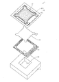
- FIG. 1 showing an embodiment of the present invention, is a perspective view showing an external appearance of an acoustic sensor. It is a disassembled perspective view of the said acoustic sensor.
- FIG. 2 is a cross-sectional view of the acoustic sensor taken along the line XX in FIG. It is a figure which shows the principal part structure of the microphone containing the said acoustic sensor. It is a figure which shows the area
- FIGS. 1 to 11 An embodiment of the present invention will be described with reference to FIGS. 1 to 11 as follows.
- FIG. 1 is a perspective view showing an external appearance of the acoustic sensor 1.
- FIG. 2 is an exploded perspective view of the acoustic sensor 1.
- 3 is a cross-sectional view of the acoustic sensor 1
- FIG. 3A is a cross-sectional view of the acoustic sensor 1 along the line XX in FIG. 1
- FIG. 4A is an enlarged view of a region 31 in FIG. 1A
- FIG. 2C is an enlarged view of a region 32 in FIG.
- the acoustic sensor 1 includes an insulating film 13, a vibration film (diaphragm) 14, and a fixed electrode on an upper surface of a silicon substrate (semiconductor substrate) 11 provided with a back chamber 12 that is a through hole.
- the plates 5 are laminated.
- the fixed electrode plate 5 includes a back plate 15 and a fixed electrode 16, and the fixed electrode 16 is disposed on the back plate 15 on the silicon substrate 11 side.
- the vibrating membrane 14 and the fixed electrode plate 5 may be arranged in reverse.
- the back plate 15 and the fixed electrode 16 are provided with a plurality of acoustic holes 17. Further, a vibrating membrane electrode pad 18 is provided at one of the four corners of the vibrating membrane 14, and a fixed electrode pad 19 is provided at one of the four corners of the fixed electrode 16.
- the vibrating membrane 14 has a stopper 23, and the fixed electrode plate 5 has a stopper 21. Further, an air gap (air gap) 22 of about 4 ⁇ m is provided between the vibrating membrane 14 and the fixed electrode 16.
- the silicon substrate 11 is made of single crystal silicon and has a thickness of about 500 ⁇ m.
- insulating films are formed on the upper and lower surfaces of the silicon substrate 11 by an oxide film.
- the vibration film 14 is made of conductive polycrystalline silicon and has a thickness of about 0.7 ⁇ m.
- the vibrating membrane 14 is a substantially rectangular thin film, and fixed portions 20 are provided at four corners.
- the vibration film 14 is disposed on the upper surface of the silicon substrate 11 so as to cover the back chamber 12, and only the four fixing portions 20 are fixed to the silicon substrate 11.
- the vibration film 14 moves up and down in response to sound pressure. Vibrate.
- the diaphragm electrode pad 18 is provided in one of the fixed portions 20.
- the back plate 15 is made of a nitride film and has a thickness of about 2 ⁇ m.
- the back plate 15 has a peripheral portion fixed to the silicon substrate 11.
- the fixed electrode plate 5 is formed by the back plate 15 and the fixed electrode 16.
- the fixed electrode 16 is made of polycrystalline silicon and has a thickness of about 0.5 ⁇ m.
- the fixed electrode 16 is provided with a fixed electrode pad 19.
- the back plate 15 and the fixed electrode 16 are provided with a plurality of acoustic holes 17 which are holes for passing sound pressure.
- the fixed electrode 16 is provided so as to correspond to the vibrating portion excluding the four corners of the vibrating membrane 14. This is because the four corners of the vibrating membrane 14 are fixed, and the capacitance between the vibrating membrane 14 and the fixed electrode 16 does not change even if the fixed electrode 16 is provided at a location corresponding to this portion.
- the acoustic hole 17 allows the sound pressure to be applied to the vibrating membrane 14 without being applied to the fixed electrode plate 5. Further, by providing the acoustic hole 17, the air in the air gap 22 can easily escape to the outside, the thermal noise is reduced, and the noise can be reduced.
- the diaphragm 14 and the fixed electrode plate 5 are provided with a stopper 23 and a stopper 21, respectively.
- the stopper 23 prevents the vibration film 14 from adhering (sticking) to the silicon substrate 11 except for the fixing portion 20, and the stopper 21 prevents the vibration film 14 and the fixed electrode plate 5 from adhering to each other. It is to prevent.
- Each size is such that the stopper 23 has a length of about 0.3 ⁇ m and the stopper 21 has a length of about 1.0 ⁇ m.
- the fixed electrode plate 5 When the acoustic sensor 1 receives sound pressure from the surface side due to the structure described above, the fixed electrode plate 5 does not move and the vibrating membrane 14 vibrates. As a result, the distance between the vibrating membrane 14 and the fixed electrode 16 changes, so that the capacitance between the vibrating membrane 14 and the fixed electrode 16 changes. Therefore, a DC voltage is applied between the vibrating membrane electrode pad 18 electrically connected to the vibrating membrane 14 and the fixed electrode pad 19 electrically connected to the fixed electrode 16, and By extracting the change as an electrical signal, the sound pressure can be detected as an electrical signal.
- FIG. 4A and 4B are diagrams showing the main configuration of the microphone 10.
- FIG. 4A is a diagram schematically showing the appearance of the microphone 10
- FIG. 4B is a block diagram of the microphone 10. As shown in FIG.
- the microphone 10 is connected to an acoustic sensor 1 and an ASIC (Application Specific Integrated Circuits, acquisition unit) 41, which are arranged on a printed circuit board 46 and surrounded by a case 42. It is the composition which is.
- the case 42 is provided with a hole 43. Then, when the sound pressure from the outside passes through the hole 43 and reaches the acoustic sensor 1, the acoustic pressure is detected by the acoustic sensor 1. Further, when light from the outside passes through the hole 43 and reaches the acoustic sensor 1, noise due to light may be generated.
- ASIC Application Specific Integrated Circuits, acquisition unit
- the ASIC 41 includes a charge pump 44 and an amplifier unit 45.
- the vibration membrane electrode pad 18 and the fixed electrode pad 19 of the acoustic sensor 1 are connected to the ASIC 41.
- the charge pump 44 is a DC power source, and applies a DC voltage between the vibrating membrane electrode pad 18 and the fixed electrode pad 19 of the acoustic sensor 1. That is, a DC voltage for detecting a change in electrostatic capacitance between the vibrating membrane 14 and the fixed electrode 16 is applied by the charge pump 44.
- the amplifier unit 45 measures the voltage between the diaphragm electrode pad 18 and the fixed electrode pad 19 of the acoustic sensor 1 and outputs the amount of change. That is, this output indicates a change in electrostatic capacitance between the vibrating membrane 14 and the fixed electrode 16 as an electrical signal, and thereby the sound pressure can be detected.
- V DD indicates a power supply voltage
- V OUT indicates an output voltage.
- FIG. 5 is a diagram showing a region to which an impurity is added.
- FIG. 6 is a figure for demonstrating the effect by adding an impurity.
- FIG. 7 is a diagram for explaining a difference in impurity concentration in a region to which an impurity is added.
- impurities are added to the surface of the silicon substrate 11. Impurities are added by ion doping. First, the reason for adding impurities will be described.
- the following effects are obtained. That is, the time until the electrons and holes generated by the light hitting the silicon substrate 11 are reduced. Therefore, the time during which current generated by the photoelectric effect flows is shortened. Thereby, the electric current which flows into the diaphragm electrode pad 18 or the fixed electrode pad 19 can be reduced, and the error of the DC voltage taken out by the ASIC 41 can be reduced.
- impurities are added to the impurity addition region 51, which is a surface on which the vibration film 14, the fixed electrode plate 5, etc. of the silicon substrate 11 are laminated. Thereby, the light noise which arises when the light which passed through the acoustic hole 17 and hits the surface of the silicon substrate 11 can be reduced.
- the region to which the impurity is added is not limited to this, and may be added to the entire surface of the silicon substrate 11 as shown in FIG. 5B, for example. Thereby, the optical noise produced by the light which entered the housing
- impurities added to the silicon substrate 11 include boron (B), phosphorus (P), arsenic (As), gold (Au), aluminum (Al), iron (Fe), chromium (Cr), and these A compound can be mentioned.
- FIG. 6 shows the result of measuring the light sensitivity by applying light to the silicon substrate 11 to which the impurity was added and the silicon substrate 11 to which the impurity was not added.
- boron is used as an impurity.
- the vertical axis indicates the sensitivity of light, and the lower it is, the less light noise is generated.
- the substrates A to F are not doped with impurities
- the substrates G to J are doped with impurities.
- the substrates G to J to which impurities are added have lower light sensitivity, that is, light noise is less likely to occur than the substrates A to F to which impurities are not added.
- FIG. 7 is a view of the silicon substrate 11 as viewed from above.
- a region 71 indicated by hatching has a high impurity concentration, and a region 72 has a low impurity concentration.
- the region 72 is a portion where the vibrating membrane electrode pad 18 and the silicon substrate 11 are electrically connected, and the electrical resistance can be increased by reducing the impurity concentration in this portion.
- FIG. 8 is a diagram illustrating a state in which a plurality of chips are manufactured on one wafer.
- FIG. 9 is a diagram showing an electrical connection relationship between a plurality of chips.
- a plurality of chips (chip a, chip b, chip c) are manufactured on one wafer 81.
- the electrical connection relationship at this time is as shown in FIG.
- the resistance value of the resistor 82 between the diaphragm electrode pad 18 and the wafer 81 is low, the diaphragm electrode pads 18 of all the chips are short-circuited. Therefore, if electrical measurement of a plurality of chips is performed simultaneously in this state, an accurate measurement result is not obtained for each chip.
- the resistance value of the resistor 82 is high, the vibrating membrane electrode pads 18 of all the chips are not short-circuited, and electrical measurement of a plurality of chips can be performed simultaneously.
- the reason why the vibration film 14 and the silicon substrate 11 are short-circuited is to prevent the acoustic sensor 1 from being destroyed when the vibration film 14 and the fixed electrode 15 are short-circuited. Instead of short-circuiting the vibration film 14 and the silicon substrate 11, the fixed electrode 16 and the silicon substrate 11 may be short-circuited.
- FIG. 10B is a cross-sectional view taken along line YY in FIG.
- the vibration film 14 and the silicon substrate 11 are connected in the region 72 of FIG. More specifically, as shown in FIG. 10B, the diaphragm electrode pad 18 and the diaphragm 14 are connected.
- the vibrating membrane electrode pad 18 is electrically connected to the region 72 on the fixed electrode plate 15, and is connected to the silicon substrate 11 in the region 72.
- FIGS. 11 and 12 are explanatory diagrams showing the manufacturing process of the acoustic sensor 1.
- the surface of the silicon substrate 101 is oxidized by a thermal oxidation method, and the surface is covered with an insulating film (SiO 2 film). Then, impurities are added to the impurity addition region 111 by ion doping (impurity addition step).
- impurities are added to the impurity addition region 111 by ion doping (impurity addition step).
- a sacrificial layer (polycrystalline silicon) 102 and a sacrificial layer (silicon oxide) 103 are deposited on the impurity-added region 111 to which impurities are added (formation step).
- a vibration film (polycrystalline silicon) 104 is formed on the upper surface of the sacrificial layer 103 (formation step).
- a sacrificial layer (silicon oxide) 105 is deposited on the vibration film 104 formed (formation step), and further a metal thin film is formed thereon.
- the fixed electrode 106 is formed, and the back plate 107 is formed by depositing silicon nitride (insulating layer) (forming step).
- An electrode pad 108 is formed by depositing gold or chromium at a predetermined position, and a hole 109 is formed in the fixed electrode 106 and the back plate 107.
- the silicon substrate 101 is etched by anisotropic etching.
- the sacrificial layer 102 is etched by isotropic etching. Further, as shown in FIG. 12B, the upper surface side of the silicon substrate 101 is etched. Then, the etching of the silicon substrate 101 is completed as shown in FIG. 12C, and finally the sacrificial layer 103 and the sacrificial layer 105 are etched as shown in FIG. Thereby, the acoustic sensor 1 is completed.
- the acoustic transducer according to the present invention includes a semiconductor substrate, a conductive vibration film, and a fixed electrode plate, and the vibration film and the fixed electrode plate have a gap on the upper surface of the semiconductor substrate.
- An acoustic transducer that is arranged and detects pressure by a change in capacitance between the vibrating membrane and the fixed electrode plate, wherein impurities are added to the surface of the semiconductor substrate. .
- the acoustic transducer manufacturing method includes a semiconductor substrate, a conductive vibration film, and a fixed electrode plate, and detects pressure by a change in capacitance between the vibration film and the fixed electrode plate.
- the region to which the impurity is added has a shorter lifetime than the region to which the impurity is not added, so that the number of electrons and holes is reduced. Therefore, the current flowing through the semiconductor substrate is reduced, and noise due to the current is reduced.
- impurities are added to the surface of the semiconductor substrate. Therefore, even if light hits the surface of the semiconductor substrate, the lifetime can be shortened, so that the number of electrons and holes generated by the photoelectric effect can be reduced. That is, the flowing current can be reduced. Thereby, since the noise by the electric current which generate
- impurities are added to the surface of the semiconductor substrate on the side where the vibration film is formed.
- the vibration film and the fixed electrode plate are formed on the side where the vibration film is formed. And when detecting a pressure by detecting a change in capacitance between the vibrating membrane and the fixed electrode plate as an electrical signal, when a current flows on the side of the semiconductor substrate where the vibrating membrane is formed, The influence on the electrical signal is large. That is, when light strikes the side of the semiconductor substrate on which the vibration film is formed, the influence of noise caused by the generated current is large.
- the surface of the semiconductor substrate and the vibrating membrane or the fixed electrode plate may be electrically connected.
- the impurity concentration in the electrically connected region of the surface of the semiconductor substrate to which the impurity is added is lower than the impurity concentration in other regions. It may be.
- the region where the impurity concentration is low is less likely to flow current than the region where the impurity concentration is high. That is, the resistance value is high. Therefore, according to said structure, the resistance value of the area
- the vibration film and the fixed electrode plate are respectively formed in a plurality of regions on one semiconductor substrate, and the acoustic transducer is formed in each region. Electrical measurements of the transducer can be made simultaneously.
- the impurities are preferably those whose lifetime is shortened by addition to the semiconductor substrate, for example, boron, phosphorus, arsenic, gold, aluminum, iron, chromium, and any of these compounds. .
- a small acoustic sensor capable of detecting sound pressure more accurately can be realized, it is suitable for a microphone of a mobile phone, for example.
Abstract
Description
まず、図1~3を用いて、本実施の形態に係る音響センサ(音響トランスデューサ)1の構造を説明する。図1は、音響センサ1の外観を示す斜視図である。また、図2は、音響センサ1の分解斜視図である。また、図3は、音響センサ1の断面図であり、同図(a)は、図1のX-X線に沿った、音響センサ1の矢視断面図であり、同図(b)は、同図(a)の領域31を拡大したものであり、同図(c)は、同図(a)の領域32を拡大したものである。 (Structure of acoustic sensor)
First, the structure of an acoustic sensor (acoustic transducer) 1 according to the present embodiment will be described with reference to FIGS. FIG. 1 is a perspective view showing an external appearance of the
本実施の形態に係るマイクロフォン10の構成について、図4を用いて説明する。図4は、マイクロフォン10の要部構成を示す図であり、同図(a)は、マイクロフォン10の外観を模式的に示す図、同図(b)は、マイクロフォン10のブロック図である。 (Configuration of microphone)
The configuration of the
次に図5~7を用いて、不純物の添加について説明する。図5は、不純物を添加する領域を示す図である。また、図6は、不純物を添加することによる効果を説明するための図である。また、図7は、不純物を添加する領域における不純物濃度の相違を説明するための図である。 (Addition of impurities)
Next, the addition of impurities will be described with reference to FIGS. FIG. 5 is a diagram showing a region to which an impurity is added. Moreover, FIG. 6 is a figure for demonstrating the effect by adding an impurity. FIG. 7 is a diagram for explaining a difference in impurity concentration in a region to which an impurity is added.
次に、図11および図12を用いて、音響センサ1の製造工程を説明する。図11および図12は、音響センサ1の製造工程を示す説明図である。 (Manufacturing process of acoustic sensor)
Next, the manufacturing process of the
以上のように、本発明に係る音響トランスデューサは、半導体基板と、導電性の振動膜と、固定電極板とを備え、上記半導体基板の上面に、上記振動膜と上記固定電極板とが空隙を設けて配置され、上記振動膜と上記固定電極板との間の静電容量の変化により圧力を検出する音響トランスデューサであって、上記半導体基板の表面に不純物が添加されていることを特徴としている。 (Other)
As described above, the acoustic transducer according to the present invention includes a semiconductor substrate, a conductive vibration film, and a fixed electrode plate, and the vibration film and the fixed electrode plate have a gap on the upper surface of the semiconductor substrate. An acoustic transducer that is arranged and detects pressure by a change in capacitance between the vibrating membrane and the fixed electrode plate, wherein impurities are added to the surface of the semiconductor substrate. .
5 固定電極板
10 マイクロフォン
11 シリコン基板(半導体基板)
12 バックチャンバー
13 絶縁膜
14 振動膜
15 バックプレート
16 固定電極
17 アコースティックホール
18 振動膜電極パッド
19 固定電極パッド
20 固定部
21、23 ストッパー
22 エアーギャップ(空隙)
41 ASIC(取得部)
101 シリコン基板
102、103、105 犠牲層
104 振動膜
106 固定電極
107 バックプレート
108 電極パッド
109 孔
111 不純物添加領域 1 Acoustic sensor (acoustic transducer)
5 Fixed
12
41 ASIC (acquisition part)
101
Claims (7)
- 半導体基板と、導電性の振動膜と、固定電極板とを備え、
上記半導体基板の上面に、上記振動膜と上記固定電極板とが空隙を設けて配置され、上記振動膜と上記固定電極板との間の静電容量の変化により圧力を検出する音響トランスデューサであって、
上記半導体基板の表面に不純物が添加されていることを特徴とする音響トランスデューサ。 A semiconductor substrate, a conductive vibration film, and a fixed electrode plate,
An acoustic transducer in which the vibrating membrane and the fixed electrode plate are arranged on the upper surface of the semiconductor substrate with a gap, and detects pressure by a change in capacitance between the vibrating membrane and the fixed electrode plate. And
An acoustic transducer, wherein impurities are added to the surface of the semiconductor substrate. - 上記半導体基板の、上記振動膜が形成されている側の表面に、不純物が添加されていることを特徴とする請求項1の記載の音響トランスデューサ。 The acoustic transducer according to claim 1, wherein an impurity is added to a surface of the semiconductor substrate on the side where the vibration film is formed.
- 上記半導体基板の上記表面と、上記振動膜または上記固定電極板とは、電気的に接続されていることを特徴とする請求項2に記載の音響トランスデューサ。 3. The acoustic transducer according to claim 2, wherein the surface of the semiconductor substrate and the vibrating membrane or the fixed electrode plate are electrically connected.
- 不純物を添加した上記半導体基板の表面のうち、上記の電気的に接続されている領域の不純物の濃度は、これ以外の領域の不純物の濃度よりも低いことを特徴とする請求項3に記載の音響トランスデューサ。 4. The impurity concentration in the electrically connected region of the surface of the semiconductor substrate to which the impurity is added is lower than the impurity concentration in other regions. Acoustic transducer.
- 上記不純物は、ボロン、リン、ヒ素、金、アルミニウム、鉄、クロム、およびこれらの化合物のいずれかであることを特徴とする請求項1~4のいずれか1項に記載の音響トランスデューサ。 5. The acoustic transducer according to claim 1, wherein the impurity is boron, phosphorus, arsenic, gold, aluminum, iron, chromium, or a compound thereof.
- 請求項1~5のいずれか1項に記載の音響トランスデューサと、該音響トランスデューサが検出した圧力の変化を取得する取得部とを備えていることを特徴とするマイクロフォン。 A microphone comprising the acoustic transducer according to any one of claims 1 to 5 and an acquisition unit that acquires a change in pressure detected by the acoustic transducer.
- 半導体基板と導電性の振動膜と固定電極板とを備え、該振動膜と該固定電極板との間の静電容量の変化により圧力を検出する音響トランスデューサの製造方法であって、
上記半導体基板の表面に不純物を添加する不純物添加ステップと、
上記不純物が添加された上記半導体基板に、上記振動膜および上記固定電極板を形成する形成ステップと、を含むことを含むことを特徴とする音響トランスデューサの製造方法。 A method of manufacturing an acoustic transducer comprising a semiconductor substrate, a conductive vibration film, and a fixed electrode plate, and detecting pressure by a change in capacitance between the vibration film and the fixed electrode plate,
An impurity addition step of adding impurities to the surface of the semiconductor substrate;
Forming a vibration film and the fixed electrode plate on the semiconductor substrate to which the impurity is added. The method of manufacturing an acoustic transducer, comprising:
Priority Applications (4)
| Application Number | Priority Date | Filing Date | Title |
|---|---|---|---|
| KR1020127030582A KR101438301B1 (en) | 2010-05-27 | 2011-04-20 | Acoustic sensor, acoustic transducer, microphone using the acoustic transducer, and method for producing acoustic transducer |
| CN2011800258003A CN102907118A (en) | 2010-05-27 | 2011-04-20 | Acoustic sensor, acoustic transducer, microphone using acoustic transducer, and method for producing acoustic transducer |
| EP11786440.5A EP2579616B1 (en) | 2010-05-27 | 2011-04-20 | Acoustic transducer and microphone using the acoustic transducer |
| US13/699,989 US8952468B2 (en) | 2010-05-27 | 2011-04-20 | Acoustic sensor, acoustic transducer, microphone using the acoustic transducer, and method for manufacturing the acoustic transducer |
Applications Claiming Priority (2)
| Application Number | Priority Date | Filing Date | Title |
|---|---|---|---|
| JP2010121681A JP5400708B2 (en) | 2010-05-27 | 2010-05-27 | Acoustic sensor, acoustic transducer, microphone using the acoustic transducer, and method of manufacturing the acoustic transducer |
| JP2010-121681 | 2010-05-27 |
Publications (1)
| Publication Number | Publication Date |
|---|---|
| WO2011148740A1 true WO2011148740A1 (en) | 2011-12-01 |
Family
ID=45003732
Family Applications (1)
| Application Number | Title | Priority Date | Filing Date |
|---|---|---|---|
| PCT/JP2011/059710 WO2011148740A1 (en) | 2010-05-27 | 2011-04-20 | Acoustic sensor, acoustic transducer, microphone using the acoustic transducer, and method for producing acoustic transducer |
Country Status (6)
| Country | Link |
|---|---|
| US (1) | US8952468B2 (en) |
| EP (1) | EP2579616B1 (en) |
| JP (1) | JP5400708B2 (en) |
| KR (1) | KR101438301B1 (en) |
| CN (1) | CN102907118A (en) |
| WO (1) | WO2011148740A1 (en) |
Cited By (3)
| Publication number | Priority date | Publication date | Assignee | Title |
|---|---|---|---|---|
| US20150293160A1 (en) * | 2012-01-31 | 2015-10-15 | Omron Corporation | Capacitive sensor |
| CN105191352A (en) * | 2013-03-14 | 2015-12-23 | 欧姆龙株式会社 | Capacitive sensor, acoustic sensor and microphone |
| CN110112116A (en) * | 2018-02-01 | 2019-08-09 | 爱思开海力士有限公司 | Semiconductor package part and the method for forming semiconductor package part |
Families Citing this family (19)
| Publication number | Priority date | Publication date | Assignee | Title |
|---|---|---|---|---|
| JP5987572B2 (en) * | 2012-09-11 | 2016-09-07 | オムロン株式会社 | Acoustic transducer |
| US9181086B1 (en) | 2012-10-01 | 2015-11-10 | The Research Foundation For The State University Of New York | Hinged MEMS diaphragm and method of manufacture therof |
| TWI528520B (en) * | 2013-03-19 | 2016-04-01 | 財團法人工業技術研究院 | Pressure sensor and manufacturing method of the same |
| GB2515836B (en) * | 2013-07-05 | 2016-01-20 | Cirrus Logic Int Semiconductor Ltd | MEMS device and process |
| JP6264969B2 (en) * | 2014-03-14 | 2018-01-24 | オムロン株式会社 | Acoustic transducer |
| JP6390423B2 (en) | 2014-12-26 | 2018-09-19 | オムロン株式会社 | Acoustic sensor and acoustic sensor manufacturing method |
| US10375482B2 (en) | 2015-03-12 | 2019-08-06 | Omron Corporation | Capacitance type transducer and acoustic sensor |
| JP6604626B2 (en) * | 2015-08-21 | 2019-11-13 | 国立大学法人東北大学 | Detection device |
| DE102015121859A1 (en) * | 2015-12-15 | 2017-06-22 | Endress+Hauser Gmbh+Co. Kg | Pressure sensor and method for operating a pressure sensor |
| JP6701825B2 (en) | 2016-03-10 | 2020-05-27 | オムロン株式会社 | Capacitive transducer and acoustic sensor |
| JP6658126B2 (en) | 2016-03-10 | 2020-03-04 | オムロン株式会社 | Capacitive transducer and acoustic sensor |
| JP6645278B2 (en) | 2016-03-10 | 2020-02-14 | オムロン株式会社 | Capacitive transducer and acoustic sensor |
| JP6809008B2 (en) | 2016-07-08 | 2021-01-06 | オムロン株式会社 | MEMS structure and capacitance type sensor, piezoelectric type sensor, acoustic sensor having MEMS structure |
| JP7143056B2 (en) | 2016-12-08 | 2022-09-28 | Mmiセミコンダクター株式会社 | capacitive transducer system, capacitive transducer and acoustic sensor |
| JP6930101B2 (en) | 2016-12-12 | 2021-09-01 | オムロン株式会社 | Acoustic sensors and capacitive transducers |
| KR102370642B1 (en) * | 2017-09-11 | 2022-03-07 | 주식회사 디비하이텍 | MEMS microphone and method of manufacturing the same |
| JP6577632B2 (en) * | 2018-06-15 | 2019-09-18 | 株式会社東芝 | Sensor |
| JP7362356B2 (en) * | 2018-12-26 | 2023-10-17 | キヤノン株式会社 | Recording material discrimination device and image forming device |
| JP7277199B2 (en) * | 2019-03-26 | 2023-05-18 | キヤノン株式会社 | IMAGE FORMING APPARATUS, IMAGE FORMING METHOD AND IMAGE FORMING SYSTEM |
Citations (2)
| Publication number | Priority date | Publication date | Assignee | Title |
|---|---|---|---|---|
| JP2009231951A (en) * | 2008-03-19 | 2009-10-08 | Panasonic Corp | Microphone device |
| JP4392466B1 (en) * | 2008-06-24 | 2010-01-06 | パナソニック株式会社 | MEMS device, MEMS device module, and acoustic transducer |
Family Cites Families (15)
| Publication number | Priority date | Publication date | Assignee | Title |
|---|---|---|---|---|
| GB2198610B (en) * | 1986-12-13 | 1990-04-04 | Spectrol Reliance Ltd | Method of producing a diaphragm on a substrate |
| US5888845A (en) * | 1996-05-02 | 1999-03-30 | National Semiconductor Corporation | Method of making high sensitivity micro-machined pressure sensors and acoustic transducers |
| JP2000022172A (en) * | 1998-06-30 | 2000-01-21 | Matsushita Electric Ind Co Ltd | Converter and manufacture thereof |
| DK1469701T3 (en) | 2000-08-11 | 2008-08-18 | Knowles Electronics Llc | Elevated microstructures |
| US6535460B2 (en) | 2000-08-11 | 2003-03-18 | Knowles Electronics, Llc | Miniature broadband acoustic transducer |
| US6987859B2 (en) | 2001-07-20 | 2006-01-17 | Knowles Electronics, Llc. | Raised microstructure of silicon based device |
| WO2003047307A2 (en) * | 2001-11-27 | 2003-06-05 | Corporation For National Research Initiatives | A miniature condenser microphone and fabrication method therefor |
| DE10160830A1 (en) | 2001-12-11 | 2003-06-26 | Infineon Technologies Ag | Micromechanical sensor comprises a counter element lying opposite a moving membrane over a hollow chamber and containing openings which are formed by slits |
| US6667189B1 (en) | 2002-09-13 | 2003-12-23 | Institute Of Microelectronics | High performance silicon condenser microphone with perforated single crystal silicon backplate |
| KR20060129041A (en) * | 2004-03-05 | 2006-12-14 | 마츠시타 덴끼 산교 가부시키가이샤 | Electret condenser |
| US7346178B2 (en) * | 2004-10-29 | 2008-03-18 | Silicon Matrix Pte. Ltd. | Backplateless silicon microphone |
| EP1922898A1 (en) * | 2005-09-09 | 2008-05-21 | Yamaha Corporation | Capacitor microphone |
| JP2007081614A (en) * | 2005-09-13 | 2007-03-29 | Star Micronics Co Ltd | Condenser microphone |
| CN101237719B (en) * | 2007-12-28 | 2012-05-23 | 深圳市豪恩电声科技有限公司 | A silicon capacitance microphone and its making method |
| US8263426B2 (en) * | 2008-12-03 | 2012-09-11 | Electronics And Telecommunications Research Institute | High-sensitivity z-axis vibration sensor and method of fabricating the same |
-
2010
- 2010-05-27 JP JP2010121681A patent/JP5400708B2/en active Active
-
2011
- 2011-04-20 WO PCT/JP2011/059710 patent/WO2011148740A1/en active Application Filing
- 2011-04-20 EP EP11786440.5A patent/EP2579616B1/en active Active
- 2011-04-20 CN CN2011800258003A patent/CN102907118A/en active Pending
- 2011-04-20 KR KR1020127030582A patent/KR101438301B1/en active IP Right Grant
- 2011-04-20 US US13/699,989 patent/US8952468B2/en active Active
Patent Citations (2)
| Publication number | Priority date | Publication date | Assignee | Title |
|---|---|---|---|---|
| JP2009231951A (en) * | 2008-03-19 | 2009-10-08 | Panasonic Corp | Microphone device |
| JP4392466B1 (en) * | 2008-06-24 | 2010-01-06 | パナソニック株式会社 | MEMS device, MEMS device module, and acoustic transducer |
Cited By (6)
| Publication number | Priority date | Publication date | Assignee | Title |
|---|---|---|---|---|
| US20150293160A1 (en) * | 2012-01-31 | 2015-10-15 | Omron Corporation | Capacitive sensor |
| US9599648B2 (en) * | 2012-01-31 | 2017-03-21 | Omron Corporation | Capacitive sensor |
| CN105191352A (en) * | 2013-03-14 | 2015-12-23 | 欧姆龙株式会社 | Capacitive sensor, acoustic sensor and microphone |
| CN105191352B (en) * | 2013-03-14 | 2018-03-02 | 欧姆龙株式会社 | Electrostatic capacity sensor, sound transducer and microphone |
| CN110112116A (en) * | 2018-02-01 | 2019-08-09 | 爱思开海力士有限公司 | Semiconductor package part and the method for forming semiconductor package part |
| US11557523B2 (en) | 2018-02-01 | 2023-01-17 | SK Hynix Inc. | Semiconductor packages and methods of forming the semiconductor packages |
Also Published As
| Publication number | Publication date |
|---|---|
| CN102907118A (en) | 2013-01-30 |
| JP2011250170A (en) | 2011-12-08 |
| JP5400708B2 (en) | 2014-01-29 |
| EP2579616B1 (en) | 2019-11-20 |
| EP2579616A1 (en) | 2013-04-10 |
| EP2579616A4 (en) | 2015-08-05 |
| KR101438301B1 (en) | 2014-09-04 |
| KR20130006512A (en) | 2013-01-16 |
| US8952468B2 (en) | 2015-02-10 |
| US20130069179A1 (en) | 2013-03-21 |
Similar Documents
| Publication | Publication Date | Title |
|---|---|---|
| JP5400708B2 (en) | Acoustic sensor, acoustic transducer, microphone using the acoustic transducer, and method of manufacturing the acoustic transducer | |
| KR101686711B1 (en) | System and method for a mems transducer | |
| Zou et al. | Design and fabrication of silicon condenser microphone using corrugated diaphragm technique | |
| TW544513B (en) | Pressure responsive device and method of manufacturing semiconductor substrate for use in the pressure responsive device | |
| JP2005039652A (en) | Sound detection mechanism | |
| WO2010140312A1 (en) | Microphone | |
| WO2011114398A1 (en) | Mems device | |
| CN105611475B (en) | Microphone sensor | |
| JP2007208549A (en) | Acoustic sensor | |
| JP2007124306A (en) | Information display device | |
| JP4737535B2 (en) | Condenser microphone | |
| JP2004128957A (en) | Acoustic detection mechanism | |
| JP2007208548A (en) | Acoustic sensor | |
| JP4244885B2 (en) | Electret condenser | |
| JP2006332799A (en) | Acoustic sensor | |
| JP5051893B2 (en) | Membrane stiffness measuring device | |
| JP2007266802A (en) | Microphone chip mounting method and microphone chip mounted by the method | |
| KR20090119268A (en) | Silicon condenser microphone and manufacturing method of silicon chip thereof | |
| JP2009118264A (en) | Microphone device | |
| JP4737720B2 (en) | Diaphragm, manufacturing method thereof, condenser microphone having the diaphragm, and manufacturing method thereof | |
| CN109405957A (en) | A kind of electric and magnetic oscillation sensor | |
| KR101108853B1 (en) | Microphone module | |
| JP4775427B2 (en) | Condenser microphone | |
| JP2007208544A (en) | Acoustic sensor | |
| JP2004096543A (en) | Acoustic detection mechanism |
Legal Events
| Date | Code | Title | Description |
|---|---|---|---|
| WWE | Wipo information: entry into national phase |
Ref document number: 201180025800.3 Country of ref document: CN |
|
| 121 | Ep: the epo has been informed by wipo that ep was designated in this application |
Ref document number: 11786440 Country of ref document: EP Kind code of ref document: A1 |
|
| WWE | Wipo information: entry into national phase |
Ref document number: 2011786440 Country of ref document: EP |
|
| ENP | Entry into the national phase |
Ref document number: 20127030582 Country of ref document: KR Kind code of ref document: A |
|
| WWE | Wipo information: entry into national phase |
Ref document number: 13699989 Country of ref document: US |
|
| NENP | Non-entry into the national phase |
Ref country code: DE |