WO2011129337A1 - Electrical component - Google Patents
Electrical component Download PDFInfo
- Publication number
- WO2011129337A1 WO2011129337A1 PCT/JP2011/059098 JP2011059098W WO2011129337A1 WO 2011129337 A1 WO2011129337 A1 WO 2011129337A1 JP 2011059098 W JP2011059098 W JP 2011059098W WO 2011129337 A1 WO2011129337 A1 WO 2011129337A1
- Authority
- WO
- WIPO (PCT)
- Prior art keywords
- circuit board
- pair
- spring member
- connection terminal
- main body
- Prior art date
Links
Images


Classifications
-
- H—ELECTRICITY
- H01—ELECTRIC ELEMENTS
- H01R—ELECTRICALLY-CONDUCTIVE CONNECTIONS; STRUCTURAL ASSOCIATIONS OF A PLURALITY OF MUTUALLY-INSULATED ELECTRICAL CONNECTING ELEMENTS; COUPLING DEVICES; CURRENT COLLECTORS
- H01R13/00—Details of coupling devices of the kinds covered by groups H01R12/70 or H01R24/00 - H01R33/00
- H01R13/02—Contact members
- H01R13/22—Contacts for co-operating by abutting
- H01R13/24—Contacts for co-operating by abutting resilient; resiliently-mounted
- H01R13/2407—Contacts for co-operating by abutting resilient; resiliently-mounted characterized by the resilient means
-
- H—ELECTRICITY
- H04—ELECTRIC COMMUNICATION TECHNIQUE
- H04N—PICTORIAL COMMUNICATION, e.g. TELEVISION
- H04N23/00—Cameras or camera modules comprising electronic image sensors; Control thereof
-
- H—ELECTRICITY
- H01—ELECTRIC ELEMENTS
- H01R—ELECTRICALLY-CONDUCTIVE CONNECTIONS; STRUCTURAL ASSOCIATIONS OF A PLURALITY OF MUTUALLY-INSULATED ELECTRICAL CONNECTING ELEMENTS; COUPLING DEVICES; CURRENT COLLECTORS
- H01R12/00—Structural associations of a plurality of mutually-insulated electrical connecting elements, specially adapted for printed circuits, e.g. printed circuit boards [PCB], flat or ribbon cables, or like generally planar structures, e.g. terminal strips, terminal blocks; Coupling devices specially adapted for printed circuits, flat or ribbon cables, or like generally planar structures; Terminals specially adapted for contact with, or insertion into, printed circuits, flat or ribbon cables, or like generally planar structures
- H01R12/50—Fixed connections
- H01R12/51—Fixed connections for rigid printed circuits or like structures
- H01R12/55—Fixed connections for rigid printed circuits or like structures characterised by the terminals
- H01R12/58—Fixed connections for rigid printed circuits or like structures characterised by the terminals terminals for insertion into holes
-
- H—ELECTRICITY
- H01—ELECTRIC ELEMENTS
- H01R—ELECTRICALLY-CONDUCTIVE CONNECTIONS; STRUCTURAL ASSOCIATIONS OF A PLURALITY OF MUTUALLY-INSULATED ELECTRICAL CONNECTING ELEMENTS; COUPLING DEVICES; CURRENT COLLECTORS
- H01R13/00—Details of coupling devices of the kinds covered by groups H01R12/70 or H01R24/00 - H01R33/00
- H01R13/66—Structural association with built-in electrical component
- H01R13/70—Structural association with built-in electrical component with built-in switch
- H01R13/703—Structural association with built-in electrical component with built-in switch operated by engagement or disengagement of coupling parts, e.g. dual-continuity coupling part
-
- H—ELECTRICITY
- H04—ELECTRIC COMMUNICATION TECHNIQUE
- H04N—PICTORIAL COMMUNICATION, e.g. TELEVISION
- H04N23/00—Cameras or camera modules comprising electronic image sensors; Control thereof
- H04N23/50—Constructional details
-
- H—ELECTRICITY
- H01—ELECTRIC ELEMENTS
- H01R—ELECTRICALLY-CONDUCTIVE CONNECTIONS; STRUCTURAL ASSOCIATIONS OF A PLURALITY OF MUTUALLY-INSULATED ELECTRICAL CONNECTING ELEMENTS; COUPLING DEVICES; CURRENT COLLECTORS
- H01R12/00—Structural associations of a plurality of mutually-insulated electrical connecting elements, specially adapted for printed circuits, e.g. printed circuit boards [PCB], flat or ribbon cables, or like generally planar structures, e.g. terminal strips, terminal blocks; Coupling devices specially adapted for printed circuits, flat or ribbon cables, or like generally planar structures; Terminals specially adapted for contact with, or insertion into, printed circuits, flat or ribbon cables, or like generally planar structures
- H01R12/70—Coupling devices
- H01R12/7005—Guiding, mounting, polarizing or locking means; Extractors
- H01R12/7011—Locking or fixing a connector to a PCB
- H01R12/7035—Locking or fixing a connector to a PCB involving non-elastic deformation, e.g. plastic deformation, melting
-
- H—ELECTRICITY
- H01—ELECTRIC ELEMENTS
- H01R—ELECTRICALLY-CONDUCTIVE CONNECTIONS; STRUCTURAL ASSOCIATIONS OF A PLURALITY OF MUTUALLY-INSULATED ELECTRICAL CONNECTING ELEMENTS; COUPLING DEVICES; CURRENT COLLECTORS
- H01R2201/00—Connectors or connections adapted for particular applications
- H01R2201/26—Connectors or connections adapted for particular applications for vehicles
Definitions
- the present invention relates to an electrical component such as a CCD camera unit mounted on an automobile as a moving body, for example.
- the CCD camera unit 101 includes a first case 102 formed in a box shape having an opening, a circuit board 104 attached (assembled) to the first case 102, and the circuit board. 104, a camera lens element 106 mounted on the circuit board 104, a spring member 103 attached to the surface of the circuit board 104 opposite to the camera lens element 106, and a second assembly that covers the opening of the first case 102.
- a case 105 and a connection terminal 107 attached to the second case 105 and electrically connected to the spring member 103 are provided (see, for example, Patent Document 1).
- the spring member 103 is elastically deformable in both directions (arrow Z direction) in a direction in which the first case 102 and the second case 105 are assembled and a direction in which the first case 102 and the second case 105 are separated from each other. Is formed. Further, the connection terminal 107 extends toward the first case 102, and when the first case 102 and the second case 105 are assembled to each other, the spring member 103 is connected to the connection terminal 107. These connection terminals 107 and the spring member 103 are electrically connected by elastic contact.
- the conventional CCD camera unit 101 described above has the following problems. That is, the conventional CCD camera unit 101 has a slight distortion or inclination caused by an assembly error between the first case 102 and the circuit board 104 or an assembly error between the first case 102 and the second case 105. Even when a positional deviation occurs from a predetermined contact point between the spring member 103 and the connection terminal 107, the positional deviation is absorbed by the spring member 103 being elastically displaced (that is, elastically deformed). Therefore, it is necessary to secure a space for the spring member 103 to be elastically deformed, and the conventional CCD camera unit 101 tends to increase in size in the direction of elastic deformation of the spring member 103 (arrow Z direction).
- the spring member 103 and the connection terminal 107 are displaced so that the spring member 103 cannot be absorbed due to elastic displacement (that is, elastic deformation) due to the vibration during traveling of the automobile described above.
- the elastic displacement amount of the spring member 103 varies, and a stable contact load cannot be maintained. Therefore, the electrical connection between the spring member 103 and the connection terminal 107 may be interrupted, and it is difficult to maintain a good connection between the spring member 103 and the connection terminal 107.
- the present invention pays attention to the above-described problems, and provides an electrical component that maintains a good connection state between the circuit board and the connection terminal connected to the circuit board and is downsized. Objective.
- An electrical component having a circuit element, a circuit board connected to the circuit element, and a connection terminal connected to the circuit board, wherein the connection terminal includes a main body part and the main body part A spring member that is elastically deformable in both directions toward and away from the circuit board, and a pair of arm portions erected from the main body so as to position the spring member between each other And the pair of arm portions are passed through the circuit board, and the end portions of the arm portions away from the main body portion are bent toward the spring member, and the end portions and the spring member are Electrical components that sandwich the circuit board between them.
- an insulating plate is provided between the circuit board and the circuit element, and the plate is disposed at a position facing the connection terminal.
- a concave portion formed in a concave shape is provided from the surface of the plate overlaid on the circuit board, and the inner peripheral surface of the concave portion is separated from the surface at a position where the end portions of the pair of arm portions abut each other. Accordingly, an electrical component provided with a pair of inclined portions inclined in a direction in which the pair of arm portions approach each other, or a pair of curved portions formed in a direction in which the pair of arm portions approach each other as the distance from the surface increases. .
- FIG. 1 is an overall perspective view of a CCD camera unit according to an embodiment of the present invention.
- FIG. 2 is an exploded perspective view showing the CCD camera unit shown in FIG. 1 in an exploded manner. It is a perspective view which shows the connection terminal which comprises the CCD camera unit shown by FIG. It is explanatory drawing for demonstrating the assembly operation of the CCD camera unit shown by FIG. 1, and is a figure which shows a mode that a connection terminal is attached to a circuit board. It is explanatory drawing for demonstrating the assembly operation of the CCD camera unit shown by FIG. 1, and is sectional drawing which shows a mode that a connection terminal passes a circuit board. It is a principal part enlarged view which expands and shows the principal part shown by FIG.
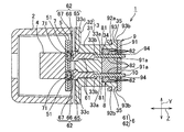
- FIG. 2 is a cross-sectional view taken along the line II shown in FIG. 1.
- FIG. 6 is an enlarged view of a main part showing a modification of the CCD camera unit shown in FIG. 1.
- FIG. 1 It is a perspective view of the conventional CCD camera unit. It is a principal part enlarged view which expands and shows the principal part shown by FIG.
- a CCD camera unit 1 as an electrical component according to an embodiment of the present invention will be described with reference to FIGS.
- a CCD camera unit 1 shown in FIGS. 1 and 2 includes a camera case 2 formed in a box shape having an opening, a connection connector 3 assembled to the camera case 2 so as to cover the opening, and the camera case 2.
- a camera lens element 4 as a circuit element accommodated in the circuit board, a circuit board 5 connected to the camera lens element 4, and a plurality of connection terminals 6 that are connected to the circuit board 5 through the connection connector 3.
- an insulating plate 7 provided between the circuit board 5 and the camera lens element 4, a mat seal 8, and a rear holder 9 attached to the connection connector 3.
- Each of the plurality of connection terminals 6 is connected to an electric wire 10.
- the plurality of electric wires 10 supply power from the power source to the camera lens element 4, or transmit a control signal to the camera lens element 4.
- the control signal from the camera lens element 4 is transmitted.
- an arrow Z shown in FIG. 1 or the like indicates a direction in which a spring member 66 of the connection terminal 6 to be described later is elastically deformed, a direction in which the connection terminal 6 approaches the circuit board 5, and the camera case 2 and the connection connector 3 Indicates the direction in which and are assembled.
- An arrow Y indicates a direction in which a pair of arm portions 67 of the connection terminal 6 described later face each other (that is, a direction in which the pair of arm portions 67 approach each other).
- An arrow X indicates a direction intersecting (orthogonal) with respect to both directions of the arrow Z and the arrow Y.
- connection connector 3 is made of an insulating synthetic resin.
- the connector 3 is provided at a rectangular connector body 31 and an end of the connector body 31 on the camera case 2 side, extends from the end in a flange shape, and opens the camera case 2. And a flange portion 32 for covering.
- the connector main body 31 has a plurality of through holes 33 through which the connection terminals 6 and the electric wires 10 to which the connection terminals 6 are attached, and a mat seal press-fit into which the mat seal 8 is press-fitted.
- locking part 35 latched to the rear holder 9 are provided.
- the plurality of through holes 33 are provided on the camera case 2 side of the connector main body 31, and the mat seal press-fit portion 34 communicates with the plurality of through holes 33 and is away from the camera case 2 of the connector main body 31. On the side.
- each through hole 33 penetrates the connector main body 31 (that is, the connection connector 3) in the arrow Z direction.
- Each through hole 33 communicates with the first through hole 33a for accommodating the electric wire 10 and the first through hole 33a, and the electric wire connecting portion 61 of the connection terminal 6 to be described later of the electric wire 10 is attached.
- the third through hole 33c is formed such that the inner diameter of the third through hole 33c is larger than those of the second through hole 33b and the first through hole 33a.
- the inner diameter of the second through hole 33b is formed larger than that of the first through hole 33a.
- the third through hole 33c is provided at the end of the connection connector 3 on the camera case 2 side, and the second through hole 33b is provided on the side farther from the camera case 2 than the third through hole 33c.
- the first through hole 33a is provided on the side farther from the camera case 2 than the second through hole 33b.
- the mat seal press-fitting portion 34 is formed in a concave shape from the end of the connector main body 31 on the side away from the camera case 2 in the arrow Z direction.
- a pair of the locking portions 35 are provided at the end of the connector main body portion 31 away from the camera case 2 in the arrow Z direction.
- the pair of locking portions 35 are formed in a convex shape in a direction away from each other in the arrow Y direction from the surface of the connector main body portion 31.
- the camera lens element 4 is connected to the circuit board 5.
- the circuit board 5 is formed with a wiring pattern that connects the camera lens element 4 and the connection terminal 6 to a predetermined pattern.
- the wiring pattern of the circuit board 5 and the camera lens element 4 are connected via an electric wire or FPC.
- the circuit board 5 is provided closer to the connection connector 3 than the camera lens element 4. Further, as shown in FIG. 4 and the like, the circuit board 5 includes a plurality of pairs of through-holes 51 through which a pair of arm portions 67 of each connection terminal 6 described later passes, and a pair of the wiring patterns. Board contact points 52 formed between the through holes 51 of each other.
- the circuit board 5 is attached to the camera case 2 so that the surface 5a on which the wiring pattern (that is, the board contact 52) is formed is directed to the connection connector 3 side.
- the circuit board 5 is positioned slightly behind the end of the camera case 2 on the side of the connection connector 3 in the arrow Z direction (side away from the connection connector 3).
- Each pair of through holes 51 of the circuit board 5 is provided at a position facing a pair of arm portions 67 of the connection terminal 6 described later along an arrow Z.
- the plural pairs of through holes 51 are provided at positions communicating with the through holes 33 of the connection connector 3.
- the pair of through holes 51 are provided along the arrow Y with a space therebetween.
- Each through hole 51 penetrates the circuit board 5 in the arrow Z direction.
- connection terminal 6 described later elastically contacts the substrate contact 52. Further, the circuit board 5 and the connection terminal 6 are electrically connected by the spring member 66 of the connection terminal 6 elastically contacting the board contact 52.
- connection terminal 6 is obtained by punching or bending a conductive sheet metal. As shown in FIG. 3 and the like, the connection terminal 6 is integrally provided with a wire connection portion 61 and an electrical contact portion 62 connected to the wire connection portion 61.
- the electric wire connecting portion 61 is integrally provided with a bottom plate 63 formed in a flat rectangular shape and a pair of core wire caulking pieces 64 erected from both edges in the width direction (arrow Y) of the bottom plate 63. ing. Moreover, the longitudinal direction (arrow Z) of the electric wire connection part 61 and the longitudinal direction of the electric wire 10 connected to this electric wire connection part 61 are provided in parallel with each other.
- the pair of core wire caulking pieces 64 are bent so that the edge on the side away from the bottom plate 63 approaches the bottom plate 63.
- the pair of core wire caulking pieces 64 are sandwiched between the bottom portion 63 and the core wire in a state where the covering portion of the electric wire 10 is peeled and exposed, and the core wire is caulked so that the core wire caulking piece 64 and the electric wire 10 core wires are electrically connected.
- the electrical contact portion 62 is formed so as to be elastically deformable in both directions (arrow Z) between a main body portion 65 continuous with the bottom plate 63 and a direction approaching and separating from the circuit board 5 provided on the main body portion 65. And a pair of arm portions 67 erected in a bar shape from the main body portion 65 in the direction of the arrow Z so as to position the spring member 66 between each other.
- the spring member 66 is provided with a space for elastically deforming the spring member 66 in the arrow Z direction.
- the space is provided at the center of the spring member 66. Further, as described above, the space is obtained by punching the connection terminal 6 into a conductive sheet metal.
- the pair of arm portions 67 are passed through the through holes 51 of the circuit board 5, and the end portions 67 a of the pair of arm portions 67 away from the main body portion 65 sandwich the circuit board 5. It is bent towards the member 66 (shown in FIG. 10). When the end portions 67a of the pair of arm portions 67 are bent toward the spring member 66 so as to sandwich the circuit board 5, the board contact 52 of the circuit board 5 and the spring member 66 are elastic. Touched.
- the plate 7 is provided with a plurality of recesses 71 that are formed in a concave shape from the surface 7a of the plate 7 superimposed on the circuit board 5.
- Each recess 71 is provided at a position communicating with each pair of through holes 51. That is, each recess 71 is provided at a position facing the connection terminal 6 along the arrow Z.
- the pair of arm portions 67 approach each other as they move away from the surface 7a of the plate 7 at the positions where the end portions 67a of the pair of arm portions 67 contact the inner peripheral surfaces of the recesses 71, respectively.
- a pair of inclined portions 71a that are inclined to each other are formed.
- the camera lens element 4 is attached to the surface 7b of the plate 7 opposite to the surface 7a.
- the mat seal 8 is made of a synthetic resin having flexibility, such as rubber, and is formed in a rectangular shape. Further, as shown in FIG. 5 and the like, the mat seal 8 is provided with an electric wire passage hole 81 through which the electric wire 10 to which the connection terminal 6 is attached and a plurality of convex portions 82 are provided. Further, the mat seal 8 prevents liquid such as water from entering the inside of the connection connector 3.
- each electric wire through hole 81 is provided at a position communicating with the through hole 33 of the connection connector 3 and penetrates the mat seal 8 in the arrow Z direction.
- the connection terminal 6 and the electric wire 10 to which the connection terminal 6 is attached are attached to the mat seal 8 by press-fitting the electric wire 10 to which the connection terminal 6 is attached into the electric wire through hole 81.
- the plurality of convex portions 82 are formed in a convex shape in a direction away from the outer surface of the mat seal 8 in the arrow Y direction. Further, the plurality of convex portions 82 are also provided on the inner surface of the electric wire through hole 81, and are formed in a convex shape in the direction of approaching each other in the arrow Y direction from the inner surface.
- the rear holder 9 includes a plate-like cover portion 91 that is superimposed on the mat seal 8 that is press-fitted into the connection connector 3, and a plurality of side wall portions that are erected from the edge of the cover portion 91 toward the mat seal 8 in the arrow Z direction. 92a, 92b, and 92c, and is formed in a bottomed cylindrical shape.
- the cover portion 91 is provided with a hole portion 94 through which the electric wire 10 to which the connection terminal 6 is attached is passed.
- a plurality of the hole portions 94 are provided.
- the plurality of holes 94 are provided at positions that communicate with the wire passage holes 81 of the mat seal 8.
- Each hole 94 penetrates the cover portion 91 in the arrow Z direction.
- a convex portion 91 a that is convex from the inner surface is formed on the inner surface of the hole portion 94.
- each of the pair of side wall portions 92a, 92b facing each other in the arrow Y direction is provided with a latch receiving portion 93 that latches to the latch portion 35 of the connection connector 3. ing.
- the locking receiving portion 93 is provided with a pair of slits 93a and a locking hole portion 93b provided between the pair of slits 93a.
- the pair of slits 93a are provided along the arrow X at intervals.
- Each slit 93a is cut out linearly from the end of the side wall portions 92a, 92b on the side away from the cover portion 91 in the arrow Z direction toward the cover portion 91.
- the said locking hole part 93b is a hole which penetrated each side wall part 92a, 92b.
- the locking receiving portion 93 is formed so as to be elastically deformable in a direction away from each other in the arrow Y direction by forming a pair of slits 93a.
- the above-described CCD camera unit 1 is assembled as follows. First, the end of the electric wire 10 is passed through the hole 94 of the rear holder 9, the electric wire through hole 81 of the mat seal 8, and the through holes 33 a, 33 b, 33 c of the connection connector 3, and the electric wire protruding from the flange portion 32. 10, the core wire in a state where the covering portion of the electric wire 10 is peeled off and exposed is placed on the bottom plate 63 of the electric wire connection portion 61 of the connection terminal 6, and the core wire caulking piece 64 is brought close to the bottom plate 63. The connection terminal 6 is attached to the electric wire 10 by caulking.
- the electric contact portion 62 of the connection terminal 6 is accommodated in the third through hole 33c, and then the electric wire 10 is While pulling away from the camera case 2 in the direction of arrow Z, only the mat seal 8 is brought close to the camera case 2 and the mat seal 8 is press-fitted into the mat seal press-fitting portion 34, and then the rear holder 9 is brought close to the camera case 2.
- connection connector 3 is locked to the locking receiving portion 93 of the rear holder 9.
- the rear holder 9 is attached to the connection connector 3.
- the rear holder 9 is attached to the connection connector 3, so that the connection terminal 6 and the electric wire 10 to which the connection terminal 6 is attached are attached to the connection connector 3 through the mat seal 8.
- the spring member 66 of the connection terminal 6 and the pair of arm portions 67 protrude from the connection connector 3 along the arrow Z.
- the circuit board 5 is mounted so that the concave portion 71 of the plate 7 and the through hole 51 of the circuit board 5 communicate with the surface 7 a of the plate 7.
- the circuit board 5 is attached to the plate 7 again.
- the camera lens element 4 and the circuit board 5 are connected via an electric wire or FPC.
- the camera lens element 4 and the circuit board 5 are connected by soldering one end of the electric wire or FPC and the camera lens element, and the other end of the electric wire or FPC and the wiring of the circuit board 5 are connected.
- the pattern is connected by soldering.
- the camera lens element 4 and the circuit board 5 are electrically connected.
- the circuit board 5 to which the camera lens element 4 is attached via the plate 7 is attached to the camera case 2.
- the circuit board 5 has the surface 5 a on which the wiring pattern is formed facing the connection connector 3, and the through holes 51 of the circuit board 5 are connected to the pair of arm portions 67 attached to the connection connector 3. It is provided so as to face each other.
- the camera case 2 and the connection connector 3 are brought close to each other so as to cover the opening of the camera case 2.
- the pair of arm portions 67 of the plurality of connection terminals 6 are passed through the through holes 51, and the end portions 67 a of the pair of arm portions 67 are moved to the plate 7. It strikes against the inclined portion 71a of the concave portion 71.
- the end portions 67a of the pair of arm portions 67 are bent toward the spring member 66 along the inclined portion 71a.
- the circuit board 5 is sandwiched between the end portions 67 a of the pair of arm portions 67 and the spring member 66.
- the connection terminal 6 and the circuit board 5 are fixed to each other by sandwiching the circuit board 5 by the pair of arm portions 67.
- the spring member 66 elastically contacts the board contact 52 of the circuit board 5, the connection terminal 6 and the circuit board 5 are electrically connected, and the camera case 2 is assembled to the connection connector 3. It is done.
- the CCD camera unit 1 is assembled.
- the connection terminal 6 is elastic in both directions (arrow Z direction) of a main body portion 65 and a direction approaching the circuit board 5 provided in the main body portion 65 and a direction away from the circuit board 5.
- a deformable spring member 66 and a pair of arm portions 67 erected from the main body portion 65 so as to position the spring member 66 between each other are provided, and the pair of arm portions 67 is the circuit.
- connection terminal 6 includes the bidirectional direction (arrow Z) in which the circuit board 5 approaches and separates from the connection terminal 6 and the direction in which the pair of arm portions 67 face each other (arrow Y). Then, the circuit board 5 is fixed so as to restrict the movement. Therefore, even when the above-described automobile vibrates during traveling, the spring member 66 maintains a stable contact load, and therefore, the circuit board 5 and the connection terminal 6 connected to the circuit board 5 are maintained. It is possible to provide the CCD camera unit 1 that maintains a good connection state.
- the circuit board 5 is fixed so as to restrict the movement of the circuit board 5 in the direction away from the connection terminal 6 (arrow Z). Accordingly, the amount of elastic displacement of the spring member 66 can be made smaller than that of the conventional spring member 66, so that the CCD camera unit 1 can be lowered (that is, downsized).
- an insulating plate 7 is provided between the circuit board 5 and the camera lens element 4, and the circuit board of the plate 7 is disposed on the plate 7 at a position facing the connection terminal 6.
- 5 is provided with a concave portion 71 formed in a concave shape from the surface 7 a superimposed on the surface 7, and the inner peripheral surface of the concave portion 71 is located at a position where the end portions 67 a of the pair of arm portions 67 abut each other.
- a pair of inclined portions 71a are provided that incline in the direction (arrow Y) in which the pair of arm portions 67 approach each other as they move away.
- the end portions 67a of the pair of arm portions 67 are guided along the inclined portion 71a and bent toward the spring member 66, and the inclined portion 71a is provided.
- the circuit board 5 and the connection terminal 6 can be connected by an easy operation of pressing the connection terminal 6 against the plate 7.
- the concave portion 71 of the plate 7 is provided with the inclined portion 71a.
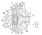
- the present invention is not limited to this, as in the CCD camera unit 1A shown in FIG. A pair of curved portions 171a formed on curved surfaces where the pair of arm portions 67 approach each other as the distance from the surface 7a increases may be provided.
- FIG. 11 the same parts as those in the above-described embodiment are denoted by the same reference numerals and description thereof is omitted.
- the end portions 67a of the pair of arm portions 67 are guided along the curved portion 171a and bent toward the spring member 66, so that the curved portion 171a is formed.
- the circuit board 5 and the connection terminal 6 can be connected by an easy operation of pressing the connection terminal 6 against the plate 7.
- the camera lens element 4 is used as a circuit element.
- the present invention is not limited to this, and various circuit elements such as a microcomputer connected to the circuit board 5 are used. Or what is necessary is just a circuit component.
- the spring member maintains a stable contact load even when the automobile vibrates during traveling, and therefore, the circuit board and the connection terminal connected to the circuit board.
- the connection state can be kept good.
Abstract
Description
(1) 回路素子と、該回路素子に接続される回路基板と、該回路基板に接続される接続端子と、を有する電装品であって、前記接続端子には、本体部と、前記本体部に設けられた前記回路基板に近付く方向と離れる方向との双方向に弾性変形自在に形成されたばね部材と、前記ばね部材を互いの間に位置付けるように前記本体部から立設した一対のアーム部と、が設けられ、前記一対のアーム部が前記回路基板を通されて、各アーム部の前記本体部から離れた端部が前記ばね部材に向かって曲げられて、前記端部と前記ばね部材との間に前記回路基板を挟んでいる電装品。 The above-described object of the present invention is achieved by the following configuration.
(1) An electrical component having a circuit element, a circuit board connected to the circuit element, and a connection terminal connected to the circuit board, wherein the connection terminal includes a main body part and the main body part A spring member that is elastically deformable in both directions toward and away from the circuit board, and a pair of arm portions erected from the main body so as to position the spring member between each other And the pair of arm portions are passed through the circuit board, and the end portions of the arm portions away from the main body portion are bent toward the spring member, and the end portions and the spring member are Electrical components that sandwich the circuit board between them.
4 カメラレンズ素子(回路素子)
5 回路基板
6 接続端子
7 プレート
65 本体部
66 ばね部材
67 アーム部
67a 端部
7a 表面
71 凹部
71a 傾斜部
171a 曲部
矢印Z 双方向
矢印Y 一対のアーム部が互いに近付く方向 1, 1A CCD camera unit (electrical equipment)
4 Camera lens elements (circuit elements)
5
Claims (2)
- 回路素子と、該回路素子に接続される回路基板と、該回路基板に接続される接続端子と、を有する電装品であって、
前記接続端子には、本体部と、
前記本体部に設けられた前記回路基板に近付く方向と離れる方向との双方向に弾性変形自在に形成されたばね部材と、
前記ばね部材を互いの間に位置付けるように前記本体部から立設した一対のアーム部と、が設けられ、
前記一対のアーム部が前記回路基板を通されて、各アーム部の前記本体部から離れた端部が前記ばね部材に向かって曲げられて、前記端部と前記ばね部材との間に前記回路基板を挟んでいる電装品。 An electrical component having a circuit element, a circuit board connected to the circuit element, and a connection terminal connected to the circuit board,
The connection terminal includes a main body part,
A spring member that is elastically deformable in both directions of approaching and separating from the circuit board provided in the main body, and
A pair of arm portions erected from the main body so as to position the spring member between each other; and
The pair of arm portions are passed through the circuit board, and the end portions of the arm portions apart from the main body portion are bent toward the spring member, and the circuit is interposed between the end portions and the spring member. Electrical components that sandwich the board. - 前記回路基板と前記回路素子との間には、絶縁性のプレートが備えられ、
前記プレートには、前記接続端子と対向する位置に、前記プレートの前記回路基板に重ねられる表面から凹状に形成された凹部が設けられ、
前記凹部の内周面には、前記一対のアーム部の前記端部それぞれが当接する位置に、前記表面から離れるにしたがって前記一対のアーム部が互いに近付く方向に傾斜する一対の傾斜部、または、前記表面から離れるにしたがって前記一対のアーム部が互いに近付く方向に形成された一対の曲部が設けられている請求項1に記載の電装品。 An insulating plate is provided between the circuit board and the circuit element,
The plate is provided with a concave portion formed in a concave shape from the surface of the plate that is superimposed on the circuit board at a position facing the connection terminal.
A pair of inclined portions that incline in a direction in which the pair of arm portions approach each other as they move away from the surface at positions where the end portions of the pair of arm portions abut each other on the inner peripheral surface of the recess, or The electrical component according to claim 1, further comprising a pair of curved portions formed in a direction in which the pair of arm portions approach each other as the distance from the surface increases.
Priority Applications (5)
| Application Number | Priority Date | Filing Date | Title |
|---|---|---|---|
| BR112012021687A BR112012021687A2 (en) | 2010-04-14 | 2011-04-12 | "electrical component" |
| CN201180011622.9A CN102782947B (en) | 2010-04-14 | 2011-04-12 | Electrical Component |
| EP11768858.0A EP2560241A4 (en) | 2010-04-14 | 2011-04-12 | Electrical component |
| US13/639,571 US8942007B2 (en) | 2010-04-14 | 2011-04-12 | Electrical component |
| KR1020127022772A KR101397768B1 (en) | 2010-04-14 | 2011-04-12 | Electrical component |
Applications Claiming Priority (2)
| Application Number | Priority Date | Filing Date | Title |
|---|---|---|---|
| JP2010093346A JP5543831B2 (en) | 2010-04-14 | 2010-04-14 | Electrical equipment |
| JP2010-093346 | 2010-04-14 |
Related Child Applications (1)
| Application Number | Title | Priority Date | Filing Date |
|---|---|---|---|
| US13/675,321 Continuation US8517949B2 (en) | 2011-05-13 | 2012-11-13 | Ultrasound transducer unit and ultrasound endoscope |
Publications (1)
| Publication Number | Publication Date |
|---|---|
| WO2011129337A1 true WO2011129337A1 (en) | 2011-10-20 |
Family
ID=44798708
Family Applications (1)
| Application Number | Title | Priority Date | Filing Date |
|---|---|---|---|
| PCT/JP2011/059098 WO2011129337A1 (en) | 2010-04-14 | 2011-04-12 | Electrical component |
Country Status (7)
| Country | Link |
|---|---|
| US (1) | US8942007B2 (en) |
| EP (1) | EP2560241A4 (en) |
| JP (1) | JP5543831B2 (en) |
| KR (1) | KR101397768B1 (en) |
| CN (1) | CN102782947B (en) |
| BR (1) | BR112012021687A2 (en) |
| WO (1) | WO2011129337A1 (en) |
Cited By (3)
| Publication number | Priority date | Publication date | Assignee | Title |
|---|---|---|---|---|
| JP2014209051A (en) * | 2013-03-29 | 2014-11-06 | パナソニック株式会社 | Refrigerator |
| JP2015135206A (en) * | 2014-01-17 | 2015-07-27 | パナソニックIpマネジメント株式会社 | refrigerator |
| CN108695607A (en) * | 2017-08-02 | 2018-10-23 | 常州星宇车灯股份有限公司 | A kind of contact connector |
Families Citing this family (6)
| Publication number | Priority date | Publication date | Assignee | Title |
|---|---|---|---|---|
| JP5573928B2 (en) * | 2012-11-29 | 2014-08-20 | Smk株式会社 | Electrical connection structure between module equipment and outside |
| JP2017083756A (en) * | 2015-10-30 | 2017-05-18 | 日本圧着端子製造株式会社 | Imaging device |
| DE102016010455B4 (en) * | 2016-08-27 | 2020-09-17 | Preh Gmbh | Sensor device for measuring the interior temperature of a motor vehicle with locking means |
| CN110972433B (en) * | 2018-09-28 | 2023-06-27 | 罗伯特·博世有限公司 | Housing for Printed Circuit Board (PCB) |
| TWI713266B (en) * | 2019-11-04 | 2020-12-11 | 大陸商東莞訊滔電子有限公司 | Electrical connector and connector assembly thereof |
| CN111479430B (en) * | 2020-04-14 | 2021-03-23 | 深圳市崧盛电子股份有限公司 | A connect waterproof construction installation and electronic product for electronic product |
Citations (4)
| Publication number | Priority date | Publication date | Assignee | Title |
|---|---|---|---|---|
| JP2001110487A (en) * | 1999-10-13 | 2001-04-20 | Denso Corp | Connection structure of flexible printed board |
| JP2003142181A (en) * | 2001-11-01 | 2003-05-16 | Furukawa Electric Co Ltd:The | Connection terminal and connecting structure for wiring body and circuit board |
| JP2009099411A (en) | 2007-10-17 | 2009-05-07 | Yazaki Corp | Contact connection structure |
| JP2010093346A (en) | 2008-10-03 | 2010-04-22 | Canon Inc | Information transmission apparatus and method of controlling the same, and computer program |
Family Cites Families (11)
| Publication number | Priority date | Publication date | Assignee | Title |
|---|---|---|---|---|
| GB9313492D0 (en) * | 1993-06-30 | 1993-08-11 | Amp Gmbh | Solderless boardblock |
| US5520545A (en) * | 1994-11-21 | 1996-05-28 | The Whitaker Corporation | Variable orientation, surface mounted hermaphroditic connector |
| US5797769A (en) * | 1996-05-14 | 1998-08-25 | Molex Incorporated | Electrical connector with boardlock |
| GB9621497D0 (en) | 1996-10-15 | 1996-12-04 | Amp Holland | Board lock for electrical connector |
| DE19726856C1 (en) * | 1997-06-24 | 1998-10-08 | Siemens Ag | Flat-plug for electrical plug-in connections |
| TW380777U (en) * | 1998-12-15 | 2000-01-21 | Hon Hai Prec Ind Co Ltd | Fixing and holding device for power connector |
| JP4299184B2 (en) | 2004-04-23 | 2009-07-22 | 矢崎総業株式会社 | Board connection board terminal |
| JP4913539B2 (en) | 2006-10-25 | 2012-04-11 | 日本圧着端子製造株式会社 | Socket contact |
| CN101212095B (en) * | 2006-12-26 | 2012-01-11 | 富士康(昆山)电脑接插件有限公司 | Electric connector terminal |
| JP5117872B2 (en) * | 2008-01-30 | 2013-01-16 | タイコエレクトロニクスジャパン合同会社 | Holding member, mounting structure in which holding member is mounted on electric circuit board, and electronic component including holding member |
| CN201285854Y (en) * | 2008-09-30 | 2009-08-05 | 富士康(昆山)电脑接插件有限公司 | Electric connector |
-
2010
- 2010-04-14 JP JP2010093346A patent/JP5543831B2/en not_active Expired - Fee Related
-
2011
- 2011-04-12 BR BR112012021687A patent/BR112012021687A2/en not_active IP Right Cessation
- 2011-04-12 CN CN201180011622.9A patent/CN102782947B/en not_active Expired - Fee Related
- 2011-04-12 US US13/639,571 patent/US8942007B2/en not_active Expired - Fee Related
- 2011-04-12 KR KR1020127022772A patent/KR101397768B1/en not_active IP Right Cessation
- 2011-04-12 WO PCT/JP2011/059098 patent/WO2011129337A1/en active Application Filing
- 2011-04-12 EP EP11768858.0A patent/EP2560241A4/en not_active Withdrawn
Patent Citations (4)
| Publication number | Priority date | Publication date | Assignee | Title |
|---|---|---|---|---|
| JP2001110487A (en) * | 1999-10-13 | 2001-04-20 | Denso Corp | Connection structure of flexible printed board |
| JP2003142181A (en) * | 2001-11-01 | 2003-05-16 | Furukawa Electric Co Ltd:The | Connection terminal and connecting structure for wiring body and circuit board |
| JP2009099411A (en) | 2007-10-17 | 2009-05-07 | Yazaki Corp | Contact connection structure |
| JP2010093346A (en) | 2008-10-03 | 2010-04-22 | Canon Inc | Information transmission apparatus and method of controlling the same, and computer program |
Non-Patent Citations (1)
| Title |
|---|
| See also references of EP2560241A4 |
Cited By (3)
| Publication number | Priority date | Publication date | Assignee | Title |
|---|---|---|---|---|
| JP2014209051A (en) * | 2013-03-29 | 2014-11-06 | パナソニック株式会社 | Refrigerator |
| JP2015135206A (en) * | 2014-01-17 | 2015-07-27 | パナソニックIpマネジメント株式会社 | refrigerator |
| CN108695607A (en) * | 2017-08-02 | 2018-10-23 | 常州星宇车灯股份有限公司 | A kind of contact connector |
Also Published As
| Publication number | Publication date |
|---|---|
| EP2560241A4 (en) | 2014-03-05 |
| BR112012021687A2 (en) | 2018-05-08 |
| CN102782947A (en) | 2012-11-14 |
| KR20120123502A (en) | 2012-11-08 |
| US20130033826A1 (en) | 2013-02-07 |
| EP2560241A1 (en) | 2013-02-20 |
| US8942007B2 (en) | 2015-01-27 |
| JP2011221457A (en) | 2011-11-04 |
| JP5543831B2 (en) | 2014-07-09 |
| KR101397768B1 (en) | 2014-05-20 |
| CN102782947B (en) | 2015-03-18 |
Similar Documents
| Publication | Publication Date | Title |
|---|---|---|
| WO2011129337A1 (en) | Electrical component | |
| JP5513232B2 (en) | Electronic components | |
| JP5615157B2 (en) | Connector and contact used for it | |
| JP4098290B2 (en) | FFC connector | |
| JP7253337B2 (en) | connector | |
| JP7208115B2 (en) | connector | |
| JP6643907B2 (en) | Connector and connection structure | |
| WO2005109580A1 (en) | Connector | |
| JP2019169370A (en) | Connector and electronic apparatus | |
| JPWO2003015221A1 (en) | connector | |
| WO2019171973A1 (en) | Connector and electronic device | |
| JP2009170310A (en) | Holding member, electronic component, and electronic device | |
| JP4597750B2 (en) | Female terminal fittings and connectors | |
| JP7353123B2 (en) | Connectors and connector assemblies | |
| WO2020022152A1 (en) | Cable connector | |
| JP4807780B2 (en) | Connector device | |
| JP7403614B2 (en) | connector | |
| CN112470555B (en) | Electronic control device | |
| JP3549851B2 (en) | connector | |
| JP2003051652A (en) | Wiring unit | |
| JP2009182190A (en) | Electric connection structure | |
| JP4170254B2 (en) | Stand-by connector holding structure | |
| JP2023115112A (en) | connector | |
| CN117791208A (en) | Connector, connector assembly and connecting method | |
| JP4845116B2 (en) | Connector device |
Legal Events
| Date | Code | Title | Description |
|---|---|---|---|
| WWE | Wipo information: entry into national phase |
Ref document number: 201180011622.9 Country of ref document: CN |
|
| 121 | Ep: the epo has been informed by wipo that ep was designated in this application |
Ref document number: 11768858 Country of ref document: EP Kind code of ref document: A1 |
|
| ENP | Entry into the national phase |
Ref document number: 20127022772 Country of ref document: KR Kind code of ref document: A |
|
| WWE | Wipo information: entry into national phase |
Ref document number: 13639571 Country of ref document: US |
|
| WWE | Wipo information: entry into national phase |
Ref document number: 8644/CHENP/2012 Country of ref document: IN |
|
| NENP | Non-entry into the national phase |
Ref country code: DE |
|
| WWE | Wipo information: entry into national phase |
Ref document number: 2011768858 Country of ref document: EP |
|
| REG | Reference to national code |
Ref country code: BR Ref legal event code: B01A Ref document number: 112012021687 Country of ref document: BR |
|
| ENP | Entry into the national phase |
Ref document number: 112012021687 Country of ref document: BR Kind code of ref document: A2 Effective date: 20120828 |