WO2011126114A1 - 照明用光源付きキーボード - Google Patents
照明用光源付きキーボード Download PDFInfo
- Publication number
- WO2011126114A1 WO2011126114A1 PCT/JP2011/058917 JP2011058917W WO2011126114A1 WO 2011126114 A1 WO2011126114 A1 WO 2011126114A1 JP 2011058917 W JP2011058917 W JP 2011058917W WO 2011126114 A1 WO2011126114 A1 WO 2011126114A1
- Authority
- WO
- WIPO (PCT)
- Prior art keywords
- key top
- movable contact
- keyboard
- circuit board
- printed circuit
- Prior art date
- Legal status (The legal status is an assumption and is not a legal conclusion. Google has not performed a legal analysis and makes no representation as to the accuracy of the status listed.)
- Ceased
Links
Images

Classifications
-
- H—ELECTRICITY
- H01—ELECTRIC ELEMENTS
- H01H—ELECTRIC SWITCHES; RELAYS; SELECTORS; EMERGENCY PROTECTIVE DEVICES
- H01H13/00—Switches having rectilinearly-movable operating part or parts adapted for pushing or pulling in one direction only, e.g. push-button switch
- H01H13/70—Switches having rectilinearly-movable operating part or parts adapted for pushing or pulling in one direction only, e.g. push-button switch having a plurality of operating members associated with different sets of contacts, e.g. keyboard
- H01H13/702—Switches having rectilinearly-movable operating part or parts adapted for pushing or pulling in one direction only, e.g. push-button switch having a plurality of operating members associated with different sets of contacts, e.g. keyboard with contacts carried by or formed from layers in a multilayer structure, e.g. membrane switches
- H01H13/705—Switches having rectilinearly-movable operating part or parts adapted for pushing or pulling in one direction only, e.g. push-button switch having a plurality of operating members associated with different sets of contacts, e.g. keyboard with contacts carried by or formed from layers in a multilayer structure, e.g. membrane switches characterised by construction, mounting or arrangement of operating parts, e.g. push-buttons or keys
-
- H—ELECTRICITY
- H01—ELECTRIC ELEMENTS
- H01H—ELECTRIC SWITCHES; RELAYS; SELECTORS; EMERGENCY PROTECTIVE DEVICES
- H01H13/00—Switches having rectilinearly-movable operating part or parts adapted for pushing or pulling in one direction only, e.g. push-button switch
- H01H13/70—Switches having rectilinearly-movable operating part or parts adapted for pushing or pulling in one direction only, e.g. push-button switch having a plurality of operating members associated with different sets of contacts, e.g. keyboard
- H01H13/83—Switches having rectilinearly-movable operating part or parts adapted for pushing or pulling in one direction only, e.g. push-button switch having a plurality of operating members associated with different sets of contacts, e.g. keyboard characterised by legends, e.g. Braille, liquid crystal displays, light emitting or optical elements
-
- H—ELECTRICITY
- H01—ELECTRIC ELEMENTS
- H01H—ELECTRIC SWITCHES; RELAYS; SELECTORS; EMERGENCY PROTECTIVE DEVICES
- H01H2203/00—Form of contacts
- H01H2203/036—Form of contacts to solve particular problems
- H01H2203/052—Form of contacts to solve particular problems for backlighted keyboards
-
- H—ELECTRICITY
- H01—ELECTRIC ELEMENTS
- H01H—ELECTRIC SWITCHES; RELAYS; SELECTORS; EMERGENCY PROTECTIVE DEVICES
- H01H2205/00—Movable contacts
- H01H2205/006—Movable contacts mounted on spacer
-
- H—ELECTRICITY
- H01—ELECTRIC ELEMENTS
- H01H—ELECTRIC SWITCHES; RELAYS; SELECTORS; EMERGENCY PROTECTIVE DEVICES
- H01H2205/00—Movable contacts
- H01H2205/016—Separate bridge contact
- H01H2205/024—Means to facilitate positioning
-
- H—ELECTRICITY
- H01—ELECTRIC ELEMENTS
- H01H—ELECTRIC SWITCHES; RELAYS; SELECTORS; EMERGENCY PROTECTIVE DEVICES
- H01H2221/00—Actuators
- H01H2221/002—Actuators integral with membrane
-
- H—ELECTRICITY
- H01—ELECTRIC ELEMENTS
- H01H—ELECTRIC SWITCHES; RELAYS; SELECTORS; EMERGENCY PROTECTIVE DEVICES
- H01H2221/00—Actuators
- H01H2221/036—Return force
- H01H2221/044—Elastic part on actuator or casing
-
- H—ELECTRICITY
- H01—ELECTRIC ELEMENTS
- H01H—ELECTRIC SWITCHES; RELAYS; SELECTORS; EMERGENCY PROTECTIVE DEVICES
- H01H2229/00—Manufacturing
- H01H2229/002—Screen printing
- H01H2229/004—Conductive ink
Definitions
- the present invention relates to an opaque front case arranged at a distance from the front surface of a printed circuit board, an arrangement hole formed in the front case, a translucent key top arranged to protrude from the arrangement hole, and a print Transparent rubber sheet that supports the key top placed between the board and the front case, the movable contact of the switch provided on the rubber sheet that is directly under the key top, and the print that is directly under the key top
- the present invention relates to a keyboard with an illumination light source provided with an illumination light source provided on a substrate, and particularly relates to a keyboard with an illumination light source in which a movable contact is formed of a material of a color that absorbs light from the light source.
- a keyboard provided with a light source for illumination is used as a keyboard for telephones, information processing terminal devices, and the like in order to facilitate discrimination of key types.
- Such a keyboard with a light source for illumination is particularly effective when used in an environment where the surroundings are dark.
- Patent Document 1 Japanese Patent Laid-Open No. 8-79354
- This conventional keyboard with a light source for illumination has a front case disposed on the front surface of a printed circuit board, an arrangement hole is formed in the front case, and an operation portion of a light-transmitting operation knob is projected from the arrangement hole. It is.
- the LEDs are arranged on the printed circuit board corresponding to the operation knobs.
- seat of high reflectance is arrange
- white printing is performed on the component placement surface of the printed circuit board to form a white printing layer.
- the conventional keyboard 100 with a light source for illumination has an opaque front case 30 arranged on the front surface of the printed circuit board 20 with an interval, and an arrangement hole 301 is formed in the front case 30.
- the rectangular key top 40 protrudes from the arrangement hole 301.
- This key top 40 is formed of a white turbid synthetic resin material having translucency, and has characters, symbols and the like written thereon.
- an elastic rubber sheet 50 made of transparent silicon rubber that is sufficiently transparent to light is disposed between the printed circuit board 20 and the front case 30, an elastic rubber sheet 50 made of transparent silicon rubber that is sufficiently transparent to light is disposed.
- the rubber sheet 50 has a key top support portion 501 formed in the same shape and thickness as the key top 40 at a position corresponding to the key top 40, and a small thickness between the key top support portion 501 and the rubber sheet main body 502. And a bent portion 503 formed as described above. Since the key top support portion 501 is always elastically biased upward by the bending portion 503, the key top 40 fixed to the upper surface of the key top support portion 501 protrudes from the arrangement hole 301. This protruding state is positioned by a positioning rod 401 formed on the peripheral edge of the key top 40 coming into contact with the lower surface of the front case 30.
- a pair of U-shaped bulges 504 are formed on the lower surface of the key top support 501 (see FIG. 7).
- the bulging portion 504 is integrally formed when the rubber sheet 50 is formed.
- a movable contact 200 is formed on the surface of the bulging portion 504 by printing carbon by silk printing.
- a fixed contact (not shown) is provided on the printed circuit board 20 facing the movable contact 200.
- a space is formed in the central portion of the key top support portion 501, and the light emitting diode 60 is disposed in this space.
- the space portion 505 is formed in such a size that the upper portion of the light emitting diode 60 does not hit the bottom surface of the key top support portion 501 even when the key top support portion 501 pushes down the movable contact 200 until it contacts the fixed contact.
- the movable contact 200 is made compact and a large space 505 is formed immediately below the key top 40, the light emitting diode 60 can be disposed in the space 505. it can. Therefore, the light from the light emitting diode 60 directly irradiates the key top 40 through the key top support portion 501.
- the opening / closing operation of the switch is such that the movable contact 200 is separated from the fixed contact because the key top support portion 501 is always biased upward by the bending portion 503, but when the key top 40 is pushed down, the bending portion 503 is The key top support portion 501 is lowered by bending. As a result, the closing operation of the switch is achieved by the movable contact 200 coming into contact with the fixed contact.
- the conventional keyboard 100 with a light source for illumination eliminates the problems of the prior art shown in Patent Document 1 by arranging the light emitting diode 60 directly below the key top 40.
- JP-A-8-79354 (paragraph 0003, paragraphs 0008 to 0010, FIG. 3)
- the movable contact in the conventional keyboard with a light source for illumination, since the movable contact is arranged below the key top support portion, the movable contact gently appears on the surface of the key top.
- the movable contact is made of a black material that absorbs light, such as carbon, there is a problem in that the movable contact remarkably rises and feels uncomfortable. Further, the amount of light from the light source to the surface of the key top is absorbed by the movable contact portion, and there is a problem that the surface of the key top is not sufficiently bright and the surface color is darkened.
- an object of the present invention is to eliminate the above-mentioned problems, and to efficiently illuminate the key top and to make the movable contact disposed on the back side of the key top unrecognizable from the key top surface.
- the object is to provide a keyboard with a light source.
- a keyboard with a light source for illumination includes an opaque front case disposed at a distance from the front surface of a printed circuit board, and an arrangement hole formed in the front case.
- a translucent key top that protrudes from the arrangement hole, a transparent rubber sheet that supports the key top disposed between the printed circuit board and the front case, and immediately below the key top
- a keyboard with an illumination light source comprising a movable contact of a switch provided on the rubber sheet and an illumination light source provided on the printed circuit board corresponding to the key top;
- the movable contact is composed of a movable contact white layer attached to the surface of the rubber sheet and a conductive layer attached to the surface of the movable contact white layer.
- the rubber sheet is provided with a printed circuit board contact surface white layer on a surface in contact with the printed circuit board excluding a position corresponding to a position directly below the key top.
- the keyboard with an illumination light source of the present invention has the following excellent effects.
- the movable contact white layer is attached to the surface of the rubber sheet located directly below the translucent key top, and the conductive contact is attached to the surface of the movable contact white layer to provide the movable contact. Since it comprised, the irradiation light from the light source distribute
- the irradiation light is reflected by the movable contact white layer and does not reach the conductive layer, it is not attenuated, so that the key top can be efficiently irradiated by the light source. Therefore, it is possible to reliably determine the key top position, type, and the like.
- the rubber sheet that contacts the printed circuit board is provided with a white layer on the printed circuit board contact surface, so that the irradiation light from the light source reaching the printed circuit board contact surface white layer is reflected to Head in the direction. Therefore, the key top can be efficiently irradiated without the light from the light source being attenuated.
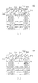
- FIG. 4 is a rear view showing a part of the rubber sheet in FIG. 1 as viewed from the lower surface side in direct contact with the printed circuit board, and FIG. 4A shows only the printed circuit board contact surface white layer and the movable contact white layer.
- FIG. 4B is a rear view showing a state where a conductive layer is attached to the surface of the movable contact white layer.
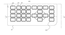
- FIG. 6 is a cross-sectional view taken along line BB in FIG. 5.
- FIG. 6 is a rear view showing a part of the rubber sheet in FIG. 5 in an enlarged manner when viewed from a lower side in direct contact with the printed circuit board.
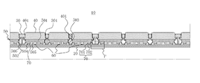
- FIG. 1 is a front view of a keyboard with an illumination light source according to an embodiment of the present invention
- FIG. 2 is a cross-sectional view taken along line AA in FIG.
- the keyboard 10 with a light source for illumination includes a printed circuit board 20, an opaque front case 30 arranged at a distance from the front surface of the printed circuit board 20, and a front case. 30, a rectangular arrangement hole 301 formed in a rectangular shape, a rectangular key top 40 protruding from the arrangement hole 301, a rubber sheet 50 disposed between the printed circuit board 20 and the front case 30, and a key
- the light-emitting diode 60 is a light source for illumination disposed on the printed circuit board 20 positioned below the top 40.
- the key top 40 is formed of a synthetic resin material that is cloudy and has translucency.
- the rubber sheet 50 is made of a transparent silicon rubber that is sufficiently transparent to light and has elasticity.
- the rubber sheet 50 includes a key top support portion 501 formed in the same shape and thickness as the key top 40 at a position corresponding to the key top 40, and a rubber sheet main body in contact with the printed circuit board 20 around the key top support portion 501. 502 and a bent portion 503 formed between the key top support portion 501 and the rubber sheet main body 502 with a reduced thickness.
- the key top 40 is fixed to the upper surface of the key top support portion 501.
- the key top 40 protrudes from the arrangement hole 301 because the key top support portion 501 is always elastically biased upward by the bending portion 503. This protruding state is positioned by a positioning rod 401 formed on the peripheral edge of the key top 40 coming into contact with the lower surface of the front case 30.
- a bulging portion 504 bulging in a pair of U shapes is formed on the lower surface of the key top support portion 501 in the rubber sheet 50. Due to the bulging portion 504, a space portion 505 is formed immediately below the key top 40.
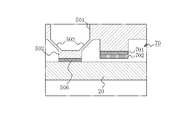
- a movable contact 70 of the switch is formed on the surface of the bulging portion 504. As shown in detail in FIG. 3, the movable contact 70 includes a movable contact white layer 701 attached to the top surface of the bulging portion 504 and a conductive layer 702 attached on the movable contact white layer 701. A fixed contact (not shown) is provided on the printed board 20 so as to face the movable contact 70.
- a movable contact white layer 701 is attached to the top surface of the bulging portion 504 as shown in FIG.
- the movable contact white layer 701 is formed into a thin film by applying a white synthetic resin material by silk printing.
- carbon is applied to the surface of the movable contact white layer 701 by silk printing to form a conductive layer 702.
- the rubber sheet 50 is in contact with the printed circuit board 20 except for the position corresponding to the position directly below the key top 40, and the printed circuit board contact surface white layer 506 is also attached to this part as a whole.
- the printed circuit board contact surface white layer 506 is formed into a thin film by applying a white synthetic resin material by silk printing. This printing is performed simultaneously with the silk printing when the movable contact white layer 701 is applied.
- the key top 40 protrudes from the arrangement hole 301 because the key top support portion 501 is always biased away from the printed circuit board 20 by the elastic force of the bending portion 503.
- the protruding position is determined by the positioning rod 401 coming into contact with the back surface of the front case 30.
- the light-emitting diode 60 emits light by receiving power supply from an electronic device to which the keyboard 10 with illumination light source is applied, and irradiates the transparent key top support portion 501 from below. This irradiation light passes through the key top support portion 501 and reaches the key top 40. As a result, since the key top 40 has translucency, it appears to shine brightly and emit light. Therefore, the position and display of the key top 40 are easy to understand and the operation becomes easy. On the other hand, since the movable contact white layer 701 is on the key top 40 side, the conductive layer 702 cannot be seen from the front of the key top 40.
- the light emitted from the light emitting diode 60 irradiates the movable contact white layer 701 and the printed circuit board contact surface white layer 506 as well as directly toward the key top indicating unit 501. Reflected in the white layers 701 and 506. The reflected light irradiates the key top 40 from the back surface in the direction of the key top indicating unit 501.
- the movable contact 70 formed on the key top support portion 501 in the rubber sheet 50 is conductive on the surface provided with the movable contact white layer 701. Since the layer 702 is provided, the conductive layer 702 is not seen through the transparent key top support portion 501 and the translucent key top 40, and the conventional conductive layer can be seen to cause a sense of incongruity.
- the irradiation light from the light emitting diode 60 reaching the movable contact 70 is reflected by the movable contact white layer 701 and reaches the key top support portion 501, and therefore reaches the conductive layer 702 and efficiently irradiates the key top 40 without attenuation. I do.
- the printed circuit board contact surface white layer 506 is attached to the rubber sheet 50 in contact with the printed circuit board 20, the light emitted from the light emitting diode 60 reaching the printed circuit board contact surface white layer 506 is reflected to reflect the key top 40. Head in the direction of Therefore, the key top 40 is efficiently irradiated without the light from the light emitting diode 60 being attenuated.
- the printed circuit board contact surface white layer 506 and the movable contact white layer 701 reflect the light of the light emitting diode 60 and the ambient light entering from the outside, so that the key of the light emitting diode 60 itself is not increased without increasing the luminance.
- the brightness of the top 40 can be improved.
- the electronic device to which the keyboard 10 with the illumination light source is applied can easily determine the position and type of the key top 40 when used in an environment where the surroundings are dark.
- the brightness of the key top 40 is not lost to the surrounding brightness, so that it can be reliably determined that the light emitting diode 60 emits light by the operation of the electronic device.
- the printed circuit board contact surface white layer 506 and the movable contact white layer 701 can be simultaneously formed on the rubber sheet 50 by silk printing, the work for forming the layer is simple.
- the key top 40 is cloudy, but the present invention is not limited to white and may be of other colors.
- the printed circuit board contact surface white layer 506 and the movable contact white layer 701 are white in color, but this color is not pure white but mixed with silver, and other highly reflective colors. It may be white mixed with.
- the key top 40 has a rectangular shape, but the present invention is not limited to this, and may have various shapes such as a circle and an ellipse.
- the shape of the movable contact 70 is U shape, the thing of various shapes, such as I shape and a rectangular shape, is applicable.
- the keyboard 10 with a light source for illumination consists of a several rectangular key, this invention is applicable to what consists of a single key, without being limited to this.
Landscapes
- Push-Button Switches (AREA)
Abstract
プリント基板の前面に間隔を置いて配された不透明のフロントケースの配置穴から透光性を有するキートップを突出して配し、プリント基板とフロントケースとの間に配された透明性のラバーシートによってキートップを支持し、キートップの直下に対応するにラバーシートに可動接点を設け、プリント基板に光源を配した構成において、キートップの前方から導電層が見えることがなく、キートップに対する照射を効率よく行うことができる照明用光源付きキーボードを提供する。可動接点70がラバーシート50の面に付された可動接点白色層701の表面に導電層702を付して形成し、キートップ40側から導電層702が見えないように構成した。
Description
本発明は、プリント基板の前面に間隔を置いて配された不透明のフロントケースと、フロントケースに形成された配置穴と、配置穴に突出して配された透光性を有するキートップと、プリント基板とフロントケースとの間に配されたキートップを支持する透明性のラバーシートと、キートップの直下に対応するラバーシートに設けられたスイッチの可動接点と、キートップの真下に対応するプリント基板上に設けられた照明用の光源とを備えた照明用光源付きキーボードに関し、特に、可動接点が光源の光を吸収する色の素材で形成されている照明用光源付きキーボードに関するものである。
近年、電話機、情報処理用端末装置などにおけるキーボードはキーの種別の判別を容易にするために照明用光源を備えたものが用いられている。このような照明用光源付きキーボードは周囲が暗い環境下において使用される場合にその効果が著しい。
この種の照明用光源付きキーボードとしては、例えば、下記の特許文献1(特開平8-79354号公報)に示す従来技術が提案されている。この従来の照明用光源付きキーボードは、プリント基板の前面にフロントケースが配され、フロントケースに配置穴が形成され、配置穴から透光性を有する操作つまみの操作部が突出して配置されたものである。
操作部を照明する手段としては、操作部の真下に光源としてのLEDを配置することが考えられるが、操作スイッチの配置スペースの関係から難しい。そこで、LEDは操作つまみ間に相当するプリント基板上に配置している。そして、LEDからの照射光は操作つまみの操作部に至るようにLEDの前方に位置するフロントケースの裏側に高反射率の光反射シートを配置する。更に、プリント基板の部品配置面には白色印刷(シルク印刷)を施して白色印刷層を形成している。その結果、操作部直下の操作スイッチを避けて配置されたLEDからの照射光は、反射シートと白色印刷層に反射して操作つまみの操作部へと至る。
しかし、上述した特許文献1に示す従来技術においては、LEDから発光される光は反射を繰り返して操作部に至るために減衰してしまう。この減衰量を低減させるためには、反射率の高い部材を用いなければならずコスト的に不利である。そこで、このような問題点を解消するために、従来は図5、図6及び図7に示す照明用光源付きキーボードが提案されている。
この従来の照明用光源付きキーボード100は、図5~図7に示すように、プリント基板20の前面に間隔を置いて不透明のフロントケース30が配され、フロントケース30に配置穴301が形成され、配置穴301に矩形状のキートップ40が突出して配置されている。このキートップ40は白濁した透光性を有する合成樹脂材で形成され、文字、記号などが記されている。プリント基板20とフロントケース30との間には十分に光を透す透明性を有するシリコンゴムからなる弾力性を有したラバーシート50が配置されている。
このラバーシート50は、キートップ40に対応する位置にキートップ40と同一形状で厚みをもって形成されたキートップ支持部501と、キートップ支持部501とラバーシート本体502との間に厚みを薄くして形成された撓み部503とからなる。キートップ支持部501が撓み部503によって常に上方に弾性的に偏倚されているので、キートップ支持部501の上面に固着されたキートップ40は配置穴301から突出している。この突出状態はキートップ40の周縁に形成された位置決め用鍔401がフロントケース30の下面に当接することにより位置決めされている。
キートップ支持部501の下面には、一対のコ字状に膨出した膨出部504が形成されている(図7参照)。この膨出部504はラバーシート50を形成するときに一体に成型される。膨出部504の表面にはカーボンをシルク印刷によって印刷することにより可動接点200が形成されている。この可動接点200に対向するプリント基板20上には固定接点(図示せず)が設けられている。キートップ支持部501の中央部分には空間が形成され、この空間に発光ダイオード60が配置されている。この空間部505はキートップ支持部501が可動接点200を固定接点に接するまで押し下げても発光ダイオード60の上部がキートップ支持部501の底面に当たらない大きさに形成されている。
上記従来の照明用光源付きキーボード100によれば、キートップ40の真下において可動接点200をコンパクトにして大きな空間部505が形成されているので、この空間部505に発光ダイオード60を配することができる。そのため、発光ダイオード60の光が直接にキートップ支持部501を介してキートップ40を照射する。一方、スイッチの開閉動作は、キートップ支持部501が撓み部503によって常に上方に偏倚されていることにより可動接点200が固定接点から離れているが、キートップ40を押し下げることにより撓み部503を撓ませてキートップ支持部501を下降させる。その結果、可動接点200が固定接点に接触することによりスイッチの閉成動作を達成させている。
従って、上記従来の照明用光源付きキーボード100は、発光ダイオード60をキートップ40の真下に配して前述した特許文献1に示す従来技術の問題点を解消したものとなる。
しかしながら、従来の照明用光源付きキーボードにおいては、キートップ支持部の下側に可動接点が配置されているので、キートップの表面に可動接点がぼんやりと浮かび上がる。特に、可動接点がカーボンのように光を吸収する黒色の素材からなる場合には、可動接点が著しく浮かび上がって違和感を与えるという問題点があった。また、光源からキートップの表面に至る光量が可動接点部分で吸収され、キートップ表面の明るさが十分に得られず表面の色が暗く沈みこんだ状態になるという問題点があった。
従って、本発明は、上記の問題点を解消することを課題とし、キートップの照明を効率的に行うと共に、キートップの裏側に配された可動接点がキートップ表面から認識できないようにした照明用光源付きキーボードを提供することを目的とするものである。
前記課題を解決するために、本願の第1発明に係る照明用光源付きキーボードは、プリント基板の前面に間隔を置いて配された不透明のフロントケースと、該フロントケースに形成された配置穴と、該配置穴に突出して配された透光性を有するキートップと、該プリント基板とフロントケースとの間に配された該キートップを支持する透明性のラバーシートと、該キートップの直下に対応するに該ラバーシートに設けられたスイッチの可動接点と、該キートップの真下に対応する該プリント基板上に設けられた照明用の光源とを備えた照明用光源付きキーボードであって、
前記可動接点は、前記ラバーシートの面に付された可動接点白色層と、該可動接点白色層の表面に付された導電層とから構成されていることを特徴とする。
前記可動接点は、前記ラバーシートの面に付された可動接点白色層と、該可動接点白色層の表面に付された導電層とから構成されていることを特徴とする。
また、本願の第2発明は、前記第1発明において、前記ラバーシートは、前記キートップの真下に対応する位置を除く前記プリント基板に接する面にプリント基板接触面白色層を付したことを特徴とする。
本発明の照明用光源付きキーボードは、次に示すような優れた効果を奏する。
即ち、第1発明においては、透光性を有するキートップの真下に位置するラバーシートの面に可動接点白色層を付し、この可動接点白色層の表面に導電層を付して可動接点を構成したので、キートップの真下に配した光源からの照射光が可動接点白色層に反射してキートップの方向に至る。従って、キートップの前方から導電層が見えなくなり、従来のように導電層が見えてしまうという違和感を解消する。また、照射光は可動接点白色層で反射し導電層に至らないので減衰することがないので、光源によるキートップに対する照射を効率よく行うことができるようになる。このため、キートップの位置、種別などの判別を確実なものとすることができる。
また、第2発明においては、プリント基板に接するラバーシートにはプリント基板接触面白色層が付されているので、プリント基板接触面白色層に至った光源からの照射光が反射してキートップの方向に向かう。そのため、光源からの光が減衰することなくキートップを効率よく照射することができるようになる。
以下、本発明の具体例を実施例及び図面を用いて詳細に説明するが、従来技術と同一部分は同一符号を付して説明する。但し、以下に示す実施例は、本発明の技術的思想を具体化するための照明用光源付きキーボードを例示するものであって、本発明をこの照明用光源付きキーボードに特定することを意図するものでなく、特許請求の範囲に含まれるその他の実施形態の照明用光源付きキーボードにも等しく適用し得るものである。
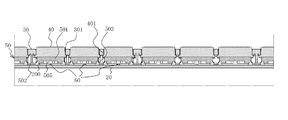
図1は本発明の一実施例に係る照明用光源付きキーボードの正面図であり、図2は図1におけるA-A線で切断した断面図である。
本実施例に係る照明用光源付きキーボード10は、図1、図2に示すように、プリント基板20と、プリント基板20の前面に間隔を置いて配された不透明のフロントケース30と、フロントケース30に矩形状に形成された配置穴301と、配置穴301に突出して配置された矩形状のキートップ40と、プリント基板20とフロントケース30との間に配されたラバーシート50と、キートップ40の下方に位置するプリント基板20上に配された照明用光源となる発光ダイオード60とから構成されている。
キートップ40は白濁して透光性を有する合成樹脂材で形成されている。ラバーシート50は光を十分に透す透明性を有するシリコンゴムからなり弾力性を有している。そして、ラバーシート50は、キートップ40に対応する位置にキートップ40と同一形状で厚みをもって形成されたキートップ支持部501と、キートップ支持部501の周辺におけるプリント基板20に接するラバーシート本体502と、キートップ支持部501とラバーシート本体502との間に厚みを薄くして形成された撓み部503とからなる。
キートップ40はキートップ支持部501の上面に固着されている。そして、キートップ40はキートップ支持部501が撓み部503によって常に上方に弾性的に偏倚されているので配置穴301から突出している。この突出状態はキートップ40の周縁に形成された位置決め用鍔401がフロントケース30の下面に当接することにより位置決めされている。
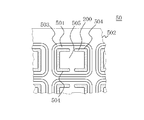
ラバーシート50におけるキートップ支持部501の下面には、図3、図4で示すように、一対のコ字状に膨出した膨出部504が形成されている。この膨出部504によって、キートップ40の真下には空間部505が形成される。膨出部504の表面にはスイッチの可動接点70が形成されている。この可動接点70は、図3で詳しく示すように、膨出部504の頂面に付された可動接点白色層701と、可動接点白色層701上に付された導電層702とからなる。プリント基板20上には可動接点70に対向して固定接点(図示せず)が設けられている。
可動接点70を形成する手順は、まず、図4(a)で示すように、膨出部504の頂面に可動接点白色層701を付す。この可動接点白色層701は白色の合成樹脂材をシルク印刷によって付され薄い膜状になっている。次に、図4(b)で示すように、可動接点白色層701の表面にカーボンをシルク印刷によって付して導電層702を形成する。
ラバーシート50はキートップ40の真下に対応する位置を除く部分がプリント基板20に接しているが、この部分にも全体にプリント基板接触面白色層506が付されている。このプリント基板接触面白色層506は白色の合成樹脂材をシルク印刷によって付され薄い膜状になっている。この印刷は可動接点白色層701を付す際のシルク印刷と同時に行われる。
次に、上述した実施例の照明用光源付きキーボード10における動作について説明する。キートップ40は、キートップ支持部501が撓み部503の弾発力によってプリント基板20から離れるように常に偏倚されているため配置穴301から突出している。そして、位置決め用鍔401がフロントケース30の背面に当接することにより突出位置の位置決めがなされている。この状態でキートップ40を押してキートップ支持部501を押し下げると、可動接点70が固定接点に接してスイッチの開閉動作を切り換える。
また、発光ダイオード60は照明用光源付きキーボード10が適用される電子機器から電力供給を受けて光を発光し透明性のキートップ支持部501を下方から照射している。この照射光はキートップ支持部501を透してキートップ40に至る。その結果、キートップ40は透光性を有するので明るく輝いて発光して見える。そのため、キートップ40の位置、表示などがわかりやすくなり操作が容易となる。一方、可動接点70は可動接点白色層701がキートップ40の側にあるのでキートップ40の前方からは導電層702を見ることができない。
発光ダイオード60から発光された光は、直接にキートップ指示部501に向かうだけでなく可動接点白色層701、プリント基板接触面白色層506に向かってこれらを照射するが、この照射光は夫々の白色層701、506において反射される。この反射光はキートップ指示部501の方向に向かってキートップ40を背面から照射することになる。
従って、上述した本発明の実施例の照明用光源付きキーボード10によれば、ラバーシート50におけるキートップ支持部501に形成されている可動接点70が可動接点白色層701を付した面上に導電層702を付して構成したので、透明性のキートップ支持部501、透光性のキートップ40を透して導電層702が見えることがなく、従来の導電層が見えることにより違和感を生じさせるという問題点を解消できる。同時に、可動接点70に至る発光ダイオード60からの照射光は可動接点白色層701に反射してキートップ支持部501に至るので、導電層702に至って減衰することなく効率のよいキートップ40に対する照射を行う。
一方、プリント基板20に接するラバーシート50にはプリント基板接触面白色層506が付されているので、プリント基板接触面白色層506に至った発光ダイオード60からの照射光は反射してキートップ40の方向に向かう。そのため、発光ダイオード60からの光が減衰することなくキートップ40を効率よく照射する。
このように、プリント基板接触面白色層506、可動接点白色層701において、発光ダイオード60の光、及び外部から入り込んだ周囲光が反射するので、発光ダイオード60自体が発光する輝度を高めることなくキートップ40の輝度を向上させることができる。その結果、照明用光源付きキーボード10を適用した電子機器は、周囲が暗い環境下で使用される場合にキートップ40の位置、種別などの判別が容易となる。一方、周囲が明るい環境下で使用される場合は、キートップ40の輝きが周囲の明るさに負けることがないので電子機器の作動により発光ダイオード60が発光していることを確実に判別できる。
また、プリント基板接触面白色層506と可動接点白色層701はラバーシート50にシルク印刷によって同時に形成することができるので、その形成のための作業が簡単である。
なお、上記実施例においては、キートップ40は白濁したものであるが、本発明は色彩が白色に限定されることなくその他の色のものであってもよい。
また、上記実施例においては、プリント基板接触面白色層506、可動接点白色層701とはその色が白色としたが、この色は純白でなく銀色が混じった白色、その他の反射率の高い色が混じった白色などであってもよい。
更に、上記実施例においては、キートップ40は矩形の形状であるが、本発明はこれに限定されることなく円形、楕円形などの種々の形状のものであってもよい。また、上記実施例においては、可動接点70の形状はコ字状であるが、I字状、矩形状などの種々の形状のものを適用することができる。また、上記実施例においては、照明用光源付きキーボード10は複数矩形のキーからなるが、本発明はこれに限定されることなく単一のキーからなるものにも適用できる。
10・・・・照明用光源付きキーボード
20・・・・プリント基板
30・・・・フロントケース
40・・・・キートップ
50・・・・ラバーシート
60・・・・発光ダイオード
70・・・・可動接点
301・・・配置穴
401・・・位置決め用鍔
501・・・キートップ支持部
502・・・ラバーシート本体
503・・・撓み部
504・・・膨出部
505・・・空間部
506・・・プリント基板接触面白色層
701・・・可動接点白色層
702・・・導電層
20・・・・プリント基板
30・・・・フロントケース
40・・・・キートップ
50・・・・ラバーシート
60・・・・発光ダイオード
70・・・・可動接点
301・・・配置穴
401・・・位置決め用鍔
501・・・キートップ支持部
502・・・ラバーシート本体
503・・・撓み部
504・・・膨出部
505・・・空間部
506・・・プリント基板接触面白色層
701・・・可動接点白色層
702・・・導電層
Claims (2)
- プリント基板の前面に間隔を置いて配された不透明のフロントケースと、該フロントケースに形成された配置穴と、該配置穴に突出して配された透光性を有するキートップと、該プリント基板とフロントケースとの間に配された該キートップを支持する透明性のラバーシートと、該キートップの直下に対応するに該ラバーシートに設けられたスイッチの可動接点と、該キートップの真下に対応する該プリント基板上に設けられた照明用の光源とを備えた照明用光源付きキーボードであって、
前記可動接点は、前記ラバーシートの面に付された可動接点白色層と、該可動接点白色層の表面に付された導電層とから構成されていることを特徴とする照明用光源付きキーボード。 - 前記ラバーシートは、前記キートップの真下に対応する位置を除く前記プリント基板に接する面にプリント基板接触面白色層を付したことを特徴とする請求項1に記載の照明用光源付きキーボード。
Applications Claiming Priority (2)
| Application Number | Priority Date | Filing Date | Title |
|---|---|---|---|
| JP2010-089960 | 2010-04-09 | ||
| JP2010089960A JP5535736B2 (ja) | 2010-04-09 | 2010-04-09 | 照明用光源付きキーボード |
Publications (1)
| Publication Number | Publication Date |
|---|---|
| WO2011126114A1 true WO2011126114A1 (ja) | 2011-10-13 |
Family
ID=44763048
Family Applications (1)
| Application Number | Title | Priority Date | Filing Date |
|---|---|---|---|
| PCT/JP2011/058917 Ceased WO2011126114A1 (ja) | 2010-04-09 | 2011-04-08 | 照明用光源付きキーボード |
Country Status (2)
| Country | Link |
|---|---|
| JP (1) | JP5535736B2 (ja) |
| WO (1) | WO2011126114A1 (ja) |
Citations (3)
| Publication number | Priority date | Publication date | Assignee | Title |
|---|---|---|---|---|
| JPH01164622U (ja) * | 1988-05-10 | 1989-11-16 | ||
| JPH05325703A (ja) * | 1992-05-19 | 1993-12-10 | Ricoh Co Ltd | キー発光装置 |
| JPH08227634A (ja) * | 1995-02-21 | 1996-09-03 | Toshiba Corp | 電子機器のキースイッチ構造 |
-
2010
- 2010-04-09 JP JP2010089960A patent/JP5535736B2/ja not_active Expired - Fee Related
-
2011
- 2011-04-08 WO PCT/JP2011/058917 patent/WO2011126114A1/ja not_active Ceased
Patent Citations (3)
| Publication number | Priority date | Publication date | Assignee | Title |
|---|---|---|---|---|
| JPH01164622U (ja) * | 1988-05-10 | 1989-11-16 | ||
| JPH05325703A (ja) * | 1992-05-19 | 1993-12-10 | Ricoh Co Ltd | キー発光装置 |
| JPH08227634A (ja) * | 1995-02-21 | 1996-09-03 | Toshiba Corp | 電子機器のキースイッチ構造 |
Also Published As
| Publication number | Publication date |
|---|---|
| JP5535736B2 (ja) | 2014-07-02 |
| JP2011222280A (ja) | 2011-11-04 |
Similar Documents
| Publication | Publication Date | Title |
|---|---|---|
| JP4917840B2 (ja) | シートスイッチモジュール | |
| US8735748B2 (en) | Keyboard structure | |
| JP4926762B2 (ja) | 発光シートモジュール | |
| US7994445B2 (en) | Sheet switch, sheet switch module and panel switch | |
| US8188397B2 (en) | Sheet switch module | |
| US7893374B2 (en) | Sheet switch module | |
| JP4959164B2 (ja) | シートスイッチ、シートスイッチモジュール及びパネルスイッチ | |
| US8168904B2 (en) | Illumination button switch assembly having lighting structure and electronic device | |
| CN102113076B (zh) | 键开关结构 | |
| KR20110006385U (ko) | 발광 키보드 | |
| KR20080024012A (ko) | 키패드 어셈블리 및 이를 구비한 휴대 단말기 | |
| JP2007053063A (ja) | シートスイッチモジュール | |
| CN107818884A (zh) | 直下式发光键盘 | |
| JP4668867B2 (ja) | 操作装置 | |
| JP2010114010A (ja) | 携帯機器の照明構造 | |
| JP2009238726A (ja) | キースイッチ構造および導光シート | |
| US10497522B2 (en) | Luminous keyboard | |
| JP5535736B2 (ja) | 照明用光源付きキーボード | |
| JP2010040385A (ja) | スイッチ装置 | |
| CN102034628B (zh) | 具有透光性的按键结构及其相关电子装置 | |
| US10629394B2 (en) | Keyswitch assembly and keyboard | |
| JP2007157384A (ja) | シートスイッチ | |
| JP2009070717A (ja) | シートスイッチ | |
| JP2009093813A (ja) | キースイッチパネル | |
| JP4172479B2 (ja) | 照光部構造とそれを使用した携帯用電子機器 |
Legal Events
| Date | Code | Title | Description |
|---|---|---|---|
| 121 | Ep: the epo has been informed by wipo that ep was designated in this application |
Ref document number: 11766014 Country of ref document: EP Kind code of ref document: A1 |
|
| NENP | Non-entry into the national phase |
Ref country code: DE |
|
| 122 | Ep: pct application non-entry in european phase |
Ref document number: 11766014 Country of ref document: EP Kind code of ref document: A1 |