WO2011122215A1 - マイクロチップの製造方法及びマイクロチップ - Google Patents
マイクロチップの製造方法及びマイクロチップ Download PDFInfo
- Publication number
- WO2011122215A1 WO2011122215A1 PCT/JP2011/054729 JP2011054729W WO2011122215A1 WO 2011122215 A1 WO2011122215 A1 WO 2011122215A1 JP 2011054729 W JP2011054729 W JP 2011054729W WO 2011122215 A1 WO2011122215 A1 WO 2011122215A1
- Authority
- WO
- WIPO (PCT)
- Prior art keywords
- substrate
- microchip
- core
- groove
- cavity
- Prior art date
- Legal status (The legal status is an assumption and is not a legal conclusion. Google has not performed a legal analysis and makes no representation as to the accuracy of the status listed.)
- Ceased
Links
Images

Classifications
-
- B—PERFORMING OPERATIONS; TRANSPORTING
- B29—WORKING OF PLASTICS; WORKING OF SUBSTANCES IN A PLASTIC STATE IN GENERAL
- B29C—SHAPING OR JOINING OF PLASTICS; SHAPING OF MATERIAL IN A PLASTIC STATE, NOT OTHERWISE PROVIDED FOR; AFTER-TREATMENT OF THE SHAPED PRODUCTS, e.g. REPAIRING
- B29C45/00—Injection moulding, i.e. forcing the required volume of moulding material through a nozzle into a closed mould; Apparatus therefor
- B29C45/17—Component parts, details or accessories; Auxiliary operations
- B29C45/26—Moulds
- B29C45/2628—Moulds with mould parts forming holes in or through the moulded article, e.g. for bearing cages
-
- B—PERFORMING OPERATIONS; TRANSPORTING
- B81—MICROSTRUCTURAL TECHNOLOGY
- B81C—PROCESSES OR APPARATUS SPECIALLY ADAPTED FOR THE MANUFACTURE OR TREATMENT OF MICROSTRUCTURAL DEVICES OR SYSTEMS
- B81C99/00—Subject matter not provided for in other groups of this subclass
- B81C99/0075—Manufacture of substrate-free structures
- B81C99/0085—Manufacture of substrate-free structures using moulds and master templates, e.g. for hot-embossing
-
- B—PERFORMING OPERATIONS; TRANSPORTING
- B01—PHYSICAL OR CHEMICAL PROCESSES OR APPARATUS IN GENERAL
- B01L—CHEMICAL OR PHYSICAL LABORATORY APPARATUS FOR GENERAL USE
- B01L3/00—Containers or dishes for laboratory use, e.g. laboratory glassware; Droppers
- B01L3/50—Containers for the purpose of retaining a material to be analysed, e.g. test tubes
- B01L3/502—Containers for the purpose of retaining a material to be analysed, e.g. test tubes with fluid transport, e.g. in multi-compartment structures
- B01L3/5027—Containers for the purpose of retaining a material to be analysed, e.g. test tubes with fluid transport, e.g. in multi-compartment structures by integrated microfluidic structures, i.e. dimensions of channels and chambers are such that surface tension forces are important, e.g. lab-on-a-chip
- B01L3/502707—Containers for the purpose of retaining a material to be analysed, e.g. test tubes with fluid transport, e.g. in multi-compartment structures by integrated microfluidic structures, i.e. dimensions of channels and chambers are such that surface tension forces are important, e.g. lab-on-a-chip characterised by the manufacture of the container or its components
-
- B—PERFORMING OPERATIONS; TRANSPORTING
- B29—WORKING OF PLASTICS; WORKING OF SUBSTANCES IN A PLASTIC STATE IN GENERAL
- B29L—INDEXING SCHEME ASSOCIATED WITH SUBCLASS B29C, RELATING TO PARTICULAR ARTICLES
- B29L2031/00—Other particular articles
- B29L2031/753—Medical equipment; Accessories therefor
-
- B—PERFORMING OPERATIONS; TRANSPORTING
- B29—WORKING OF PLASTICS; WORKING OF SUBSTANCES IN A PLASTIC STATE IN GENERAL
- B29L—INDEXING SCHEME ASSOCIATED WITH SUBCLASS B29C, RELATING TO PARTICULAR ARTICLES
- B29L2031/00—Other particular articles
- B29L2031/756—Microarticles, nanoarticles
Definitions
- the present invention relates to a microchip manufacturing method and a microchip.
- ⁇ TAS MicroTotalTAnalysis Systems
- the microchip is formed by forming fine flow paths and spaces in a substrate made of silicon, glass, resin, or the like using a fine processing technique and bonding it to another substrate.
- a substrate made of silicon, glass, resin, or the like
- fine processing technique e.g., silicon dioxide, silicon dioxide, silicon dioxide, silicon dioxide, silicon dioxide, silicon dioxide, silicon dioxide, silicon dioxide, silicon dioxide, silicon dioxide, silicon dioxide, silicon dioxide, silicon dioxide, silicon dioxide, silicon dioxide, glass, resin, or the like.
- development of inexpensive and disposable resin microchips has been particularly desired.
- ⁇ Microchips are required to have channels and spaces with different depths depending on the reaction, separation, and analysis methods.
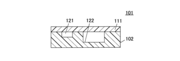
- FIG. 4 in the microchip 101 formed by bonding the substrate 102 and the lid plate 111, non-penetrating grooves 121 and 122 having different depths may coexist on one substrate 102 (for example, Patent Document 1).
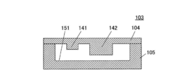
- a core plate 104 having a template 105 having a cavity 151 and ridges 141 and 142 having shapes corresponding to the non-penetrating grooves 121 and 122.
- the molten resin is injected into a mold 103 using the above and molded.
- the core 104 is formed by electroforming.
- the Ni—P plating 109 is formed on the base material 108.
- grooves 191 and 192 having the same shape as the flow path formed in the substrate are formed on the surface of the Ni—P plating 109.
- the core 104 is formed on the surface of the Ni—P plating 109 by electrolytic plating. Thereafter, by peeling from the Ni—P plating 109, the core 104 having the protrusion 141 having a shape corresponding to the groove 191 is formed.
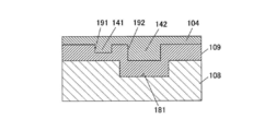
- the thickness of the Ni—P plating 109 is about 150 ⁇ m at the maximum, and in order to form a groove 192 having a depth larger than that, the base material 108 is processed as shown in FIG. 181 needs to be formed. For this reason, there is a problem that the processing time is increased and the processing time is increased.
- An object of the present invention is to provide a microchip manufacturing method and a microchip that can reduce the occurrence of sink marks with less labor of processing.
- the first invention provides a mold plate in which a cavity is provided on one surface and an insertion groove is provided in the bottom of the cavity, and a surface in which the cavity of the template plate is provided.
- a molten resin is injected and filled into the cavity of the mold, the core being in contact with the surface facing the core, and the core pin having a shape corresponding to the insertion groove inserted into the insertion groove and in contact with the core.
- a microchip manufacturing comprising: a first step of forming a substrate on which a through groove having a shape corresponding to the core pin is formed by taking out; and a second step of bonding a bottom plate and a cover plate to both surfaces of the substrate. Is the method.
- a protrusion that is lower than the depth of the cavity is provided on a contact surface of the core with the template, and a shape corresponding to the protrusion is formed on the contact surface of the substrate with the core.
- a non-through groove may be formed.
- the core is formed with Ni-P plating on the base material, and then a non-penetrating groove having a shape corresponding to the protrusion is formed on the surface of the Ni-P plating, and then the Ni-P plating After forming the electroplating on the surface, the Ni—P plating may be peeled off.
- a microchip comprising: a substrate having a through groove penetrating vertically; and a bottom plate bonded to the lower surface of the substrate.
- a lid plate joined to the upper surface of the substrate may be further provided.
- the substrate may have a non-penetrating groove on at least one surface.
- FIG. 6 is an explanatory diagram of a method for manufacturing the core 4.
- FIG. 2 is a cross-sectional view of a mold 103 used for manufacturing a substrate 102.
- FIG. 6 is an explanatory diagram of a manufacturing method of the core 104.
- FIG. 1 is a cross-sectional view showing a microchip 1 according to an embodiment of the present invention.
- the size of the microchip 1 may be any shape as long as it is easy to handle and analyze.
- the size is preferably about 10 mm square to 200 mm square, and more preferably 10 mm square to 100 mm square.
- the shape of the microchip 1 may be adjusted to an analysis method and an analysis apparatus, and may be an arbitrary shape such as a square, a rectangle, or a circle.
- the microchip 1 is formed by bonding a substrate 2, a lid plate 11, and a bottom plate 12.
- Resin is used for the substrate 2, the cover plate 11, and the bottom plate 12.
- the resin include good moldability (transferability and releasability), high transparency, and low autofluorescence with respect to ultraviolet rays and visible light, but are not particularly limited. Absent.
- polymethyl methacrylate, cyclic polyolefin and the like are preferable.
- the same material may be used for the substrate 2, the cover plate 11, and the bottom plate 12, or different materials may be used.
- the lid plate 11 is bonded to the upper surface of the substrate 2.
- the bottom plate 12 is bonded to the lower surface of the substrate 2.
- the joining method of the cover plate 11 and the substrate 2 and the bottom plate 12 and the substrate 2 is arbitrary, such as a method using an adhesive or a method using a thermal welding technique.
- the substrate 2 is provided with non-penetrating grooves 21 and penetrating grooves 22.
- the non-through groove 21 is formed on the upper surface of the substrate 2.
- the flow path 13 is formed by the upper part of the non-penetrating groove 21 being closed by the cover plate 11.
- the through groove 22 penetrates the substrate 2 up and down.
- the flow path 14 is formed by closing the through groove 22 with the bottom plate 12 and the cover plate 11.
- the flow paths 13 and 14 are very fine grooves (micro flow paths), and are suitably used for performing reaction, mixing, separation, analysis, etc. of liquid samples such as nucleic acids, proteins, blood and drugs.
- the widths of the non-penetrating groove 21 and the penetrating groove 22 are about 10 ⁇ m to 200 ⁇ m in consideration of reducing the amount of analysis sample and reagent used, forming mold forming accuracy, transferability, releasability, and the like. It is preferable.
- the depth of the non-penetrating groove 21 is preferably about 30 ⁇ m to 150 ⁇ m, and is preferably shallower than the thickness of the substrate 2.
- the depth of the flow path 14 formed by the through groove 22 is determined by the thickness of the substrate 2.
- the thickness of the substrate 2 is preferably larger than 30 ⁇ m and not more than 200 ⁇ m, but may be appropriately adjusted according to the use of the microchip 1, the analysis technique, and the analysis apparatus.
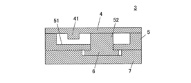
- FIG. 2 is a cross-sectional view of the mold 3 used for manufacturing the substrate 2.
- the mold 3 is roughly composed of a core 4, a mold plate 5, a core pin 6, a holding plate 7, and the like.
- the core 4 is provided with a protrusion 41 corresponding to the non-penetrating groove 21 on the surface facing the template 5.
- the template 5 is provided with a cavity 51 in which the substrate 2 is formed on the surface facing the core 4.
- An insertion groove 52 having a shape corresponding to the through groove 22 is provided at a position corresponding to the through groove 22 at the bottom of the cavity 51.
- the core pin 6 has a shape corresponding to the through groove 22 and the insertion groove 52, and is in contact with the core 4 through the template 5 from the insertion groove 52.
- the holding plate 7 is fixed to the surface of the template 5 opposite to the core 4 and holds the core pin 6 in a state of being in contact with the core 4 through the insertion plate 52 through the template 5.
- the molten resin used as the material of the substrate 2 is injected and filled into the cavity 51 of the mold 3 in the state shown in FIG. 2, and the substrate 2 is molded by cooling.
- the trace of the protrusion 41 becomes the non-penetrating groove 21, and the trace of the core pin 6 becomes the through groove 22.
- the holding plate 7 is removed from the template 5, the core pin 6 is pulled out from the insertion groove 52, the core 4 is separated from the template 5, and the substrate 2 is taken out from the cavity 51. Thereafter, the bottom plate 12 is bonded to the lower surface of the substrate 2 and the lid plate 11 is bonded to the upper surface, whereby the microchip 1 is completed. Note that the lid plate 11 may be held without being joined to the upper surface of the substrate 2 (in order to facilitate an operation such as applying a reaction solution in the flow paths 13 and 14).
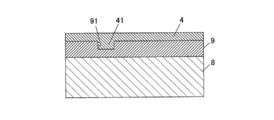
- the plating layer 9 is formed on the base material 8.
- the plating layer 9 can be formed using, for example, a Ni—P alloy.
- a non-penetrating groove 91 having the same shape as the non-penetrating groove 21 is formed on the surface of the plating layer 9.
- the depth of the non-penetrating groove 91 is shallower than the thickness of the plating layer 9.
- the non-penetrating groove 91 can be formed by etching, for example.
- the core 4 is formed on the surface of the plating layer 9 by electrolytic plating. Then, the core 4 which has the protrusion 41 of the shape corresponding to the non-through-groove 91 is formed by peeling from the plating layer 9.
- both the flow path formed by the non-through groove 21 and the flow path formed by the through groove 22 are provided.
- the present invention is not limited to this, and the Ni—P plating is provided. You may apply this invention to the microchip which has only a flow path deeper than this thickness.
- a protrusion may be formed on the bottom of the cavity 51, and a non-penetrating groove having a shape corresponding to the protrusion may be formed on the surface of the substrate 2 on the cavity 51 side.
Landscapes
- Engineering & Computer Science (AREA)
- Manufacturing & Machinery (AREA)
- Mechanical Engineering (AREA)
- Microelectronics & Electronic Packaging (AREA)
- Micromachines (AREA)
- Moulds For Moulding Plastics Or The Like (AREA)
- Physical Or Chemical Processes And Apparatus (AREA)
Abstract
加工の手間を減らすことができるマイクロチップの製造方法及びマイクロチップを提供することを目的とし、一方の面にキャビティ51が設けられるとともに、キャビティ51の底部に挿入溝52が設けられた型板5と、型板5のキャビティ51が設けられた面と対向する面に当接するコア4と、挿入溝52に挿入されコア4と当接する、挿入溝52と対応する形状のコアピン6と、からなる金型3のキャビティ51内に溶融樹脂を射出充填し、成形後、取り出すことでコアピン6と対応する形状の貫通溝22が形成された基板2を形成する第1工程と、基板2の両面に底板12及び蓋板11を接合する第2工程と、を備えるマイクロチップ1の製造方法である。
Description
本発明は、マイクロチップの製造方法及びマイクロチップに関する。
微細な流路、空間内で核酸、タンパク質、血液などの液体試料の反応、分離、分析などを行うマイクロチップ、あるいはμTAS(MicroTotal Analysis Systems)と称する装置が実用化されている。
マイクロチップは、微細加工技術を利用してシリコン、ガラス、樹脂等の基板に微細な流路、空間を形成し、他の基板と接合して形成される。近年では、廉価で使い捨て可能な樹脂製マイクロチップの開発が特に望まれている。
マイクロチップには、反応、分離、分析の方法によって深さの異なる流路、空間が求められる。例えば図4に示すように、基板102と蓋板111とを接合してなるマイクロチップ101において、1枚の基板102に深さの異なる非貫通溝121、122が並存する場合がある(例えば、特許文献1参照)。
流路を有する樹脂性の基板を形成するには、図5に示すように、キャビティ151を有する型板105と、非貫通溝121、122と対応する形状の突条141、142を有するコア104とを用いた金型103に溶融樹脂を射出して成形する。このコア104は、電鋳により成形する。
まず、図6に示すように、母材108にNi-Pめっき109を形成する。次に、Ni-Pめっき109の表面に基板に形成する流路と同じ形状の溝191、192を形成する。次に、電解めっきにより、Ni-Pめっき109の表面にコア104を形成する。その後、Ni-Pめっき109から剥離することで、溝191と対応する形状の突条141を有するコア104が形成される。
しかし、Ni-Pめっき109の厚さは最大で150μm厚程度であり、それ以上の深さの溝192を形成するためには、図6に示すように、母材108を加工して下穴181を形成する必要がある。このため、加工の手間が増え、加工時間が長くなるという問題がある。
また、1枚の基板に深さの異なる溝を並存させると、偏肉構造となり、基板にひけが発生しやすくなる。
本発明の課題は、加工の手間が少なくひけの発生を抑制することができるマイクロチップの製造方法及びマイクロチップを提供することである。
以上の課題を解決するため、第1の発明は、一方の面にキャビティが設けられるとともに、前記キャビティの底部に挿入溝が設けられた型板と、前記型板の前記キャビティが設けられた面と対向する面に当接するコアと、前記挿入溝に挿入され前記コアと当接する、前記挿入溝と対応する形状のコアピンと、からなる金型の前記キャビティ内に溶融樹脂を射出充填し、成形後、取り出すことで前記コアピンと対応する形状の貫通溝が形成された基板を形成する第1工程と、前記基板の両面に底板及び蓋板を接合する第2工程と、を備えるマイクロチップの製造方法である。
第1の発明に係る前記コアの前記型板との当接面に、前記キャビティの深さよりも低い突条を設け、前記基板の前記コアとの当接面に、前記突条と対応する形状の非貫通溝を形成してもよい。
前記コアを、母材にNi-Pめっきを形成し、次に、前記Ni-Pめっきの表面に、前記突条と対応する形状の非貫通溝を形成し、次に、前記Ni-Pめっきの表面に電解めっきを形成した後、前記Ni-Pめっきから剥離することで形成してもよい。
第2の発明は、上下に貫通する貫通溝を有する基板と、前記基板の下面に接合される底板と、を備えることを特徴とするマイクロチップである。
前記基板の上面に接合される蓋板をさらに備えてもよい。
前記基板は少なくとも一方の面に非貫通溝を有していてもよい。
本発明によれば、加工の手間が少なくひけの発生を抑制することができるマイクロチップの製造方法及びマイクロチップを提供することができる。
以下、本発明を実施するための形態について、図を参照して詳細に説明する。
図1は本発明の実施の形態に係るマイクロチップ1を示す断面図である。マイクロチップ1の大きさは、ハンドリング、分析しやすい形状であればどのような形状であってもよい。例えば、10mm角~200mm角程度の大きさが好ましく、10mm角~100mm角がより好ましい。マイクロチップ1の形状は、分析手法、分析装置に合わせればよく、正方形、長方形、円形など任意の形状とすることができる。
マイクロチップ1は、基板2と、蓋板11と、底板12とが接合されてなる。
基板2、蓋板11、底板12には樹脂が用いられる。その樹脂としては、成形性(転写性、離型性)がよいこと、透明性が高いこと、紫外線や可視光に対する自己蛍光性が低いことなどが条件として挙げられるが、特に限定されるものではない。例えば、ポリカーボネート、ポリメタクリル酸メチル、ポリスチレン、ポリアクリロニトリル、ポリ塩化ビニル、ポリエチレンテレフタレート、ナイロン6、ナイロン66、ポリ酢酸ビニル、ポリ塩化ビニリデン、ポリプロピレン、ポリイソプレン、ポリエチレン、ポリジメチルシロキサン、環状ポリオレフィン等が好ましい。特に、ポリメタクリル酸メチル、環状ポリオレフィン等が好ましい。基板2、蓋板11、底板12に同じ材料を用いてもよく、異なる材料を用いてもよい。
蓋板11は、基板2の上面に接合されている。底板12は、基板2の下面に接合されている。蓋板11と基板2、底板12と基板2の接合方法は、接着剤を用いる方法、熱溶着技術を用いる方法等、任意である。
基板2には、非貫通溝21と、貫通溝22とが設けられている。
非貫通溝21は基板2の上面に形成されている。非貫通溝21の上部が蓋板11により塞がれることで流路13が形成される。
貫通溝22は基板2を上下に貫通している。貫通溝22が底板12及び蓋板11により塞がれることで流路14が形成される。
流路13、14は、非常に微細な溝(マイクロ流路)であり、核酸、タンパク質、血液や薬剤などの液体試料の反応、混合、分離、分析などを行うのに好適に用いられる。
非貫通溝21及び貫通溝22の幅は、分析試料、試薬の使用量を少なくできること、成形金型の作成精度、転写性、離型性等を考慮して、幅は10μm~200μm程度であることが好ましい。
非貫通溝21の深さは、30μm~150μm程度であることが好ましく、基板2の厚さよりも浅いことが好ましい。
貫通溝22により形成される流路14の深さは基板2の厚さによって定まる。基板2の厚さは30μmよりも厚くかつ200μm以下であることが好ましいが、マイクロチップ1の用途、分析手法、分析装置に応じて適宜調整すればよい。
図2は、基板2の製造に用いる金型3の断面図である。金型3は、コア4と、型板5と、コアピン6と、保持板7と、等から概略構成される。
コア4には、型板5との対向面に、非貫通溝21と対応する突条41が設けられている。
型板5には、コア4との対向面に、基板2が形成されるキャビティ51が設けられている。キャビティ51の底部には、貫通溝22と対応する位置に、貫通溝22と対応する形状の挿入溝52が設けられている。
コアピン6は、貫通溝22及び挿入溝52と対応する形状をしており、挿入溝52から型板5を貫通してコア4と当接している。
保持板7は、型板5のコア4とは反対側の面に固定され、コアピン6を挿入溝52から型板5を貫通してコア4と当接した状態で保持する。
図2に示す状態の金型3のキャビティ51内に基板2の材料となる溶融樹脂を射出充填し、冷却することで基板2が成形される。なお、突条41の跡が非貫通溝21に、コアピン6の跡が貫通溝22となる。
その後、保持板7を型板5から外し、コアピン6を挿入溝52から引き出し、型板5からコア4を離してからキャビティ51から基板2を取り出す。その後、基板2の下面に底板12を、上面に蓋板11を接合することで、マイクロチップ1が完成する。なお、(流路13、14内に反応液を塗布する等の操作を容易とするために、)基板2の上面に蓋板11を接合しない状態で留めてもよい。
ここで、コア4の製造方法について図3を用いて説明する。まず、母材8にめっき層9を形成する。めっき層9は、例えばNi-P合金を用いて形成することができる。
次に、めっき層9の表面に、非貫通溝21と同一形状の非貫通溝91を形成する。非貫通溝91の深さはめっき層9の厚さよりも浅い。非貫通溝91は例えばエッチングにより形成することができる。
次に、電解めっきにより、めっき層9の表面にコア4を形成する。その後、めっき層9から剥離することで、非貫通溝91と対応する形状の突条41を有するコア4が形成される。
このように、めっき層9の厚さよりも浅い非貫通溝91を形成するのみであるため、母材8を加工する手間がない。したがって、めっき層9の厚さよりも深い流路を有するマイクロチップを形成する場合でも、加工の手間を減らし、加工時間を短縮することができる。
また、1枚の基板に深さの異なる溝を並存させると、偏肉構造となり、基板にひけが発生しやすくなるが、基板2は単一の深さの非貫通溝21と、貫通溝22のみが設けられているため、ひけが発生しない。
なお、以上の実施形態においては、非貫通溝21により形成される流路と貫通溝22により形成される流路の両方を備える構成としたが、本発明はこれに限らず、Ni-Pめっきの厚さよりも深い流路のみを有するマイクロチップに本発明を適用してもよい。
また、キャビティ51の底部に突条を形成し、基板2のキャビティ51側の面に突条と対応する形状の非貫通溝を形成してもよい。
1、101 マイクロチップ
11、111 蓋板
12 底板
2、102 基板
21、121、122 非貫通溝
22 貫通溝
3、103 金型
4、104 コア
41、141 突条
5 型板
51 キャビティ
52 挿入溝
6 コアピン
7 保持板
8、108 母材
181 下穴
9、109 Ni-Pめっき
91 非貫通溝
11、111 蓋板
12 底板
2、102 基板
21、121、122 非貫通溝
22 貫通溝
3、103 金型
4、104 コア
41、141 突条
5 型板
51 キャビティ
52 挿入溝
6 コアピン
7 保持板
8、108 母材
181 下穴
9、109 Ni-Pめっき
91 非貫通溝
Claims (6)
- 一方の面にキャビティが設けられるとともに、前記キャビティの底部に挿入溝が設けられた型板と、
前記型板の前記キャビティが設けられた面と対向する面に当接するコアと、
前記挿入溝に挿入され前記コアと当接する、前記挿入溝と対応する形状のコアピンと、からなる金型の前記キャビティ内に溶融樹脂を射出充填し、成形後、取り出すことで前記コアピンと対応する形状の貫通溝が形成された基板を形成する第1工程と、
前記基板の両面に底板及び蓋板を接合する第2工程と、
を備えることを特徴とするマイクロチップの製造方法。 - 前記コアの前記型板との当接面に、前記キャビティの深さよりも低い突条を設け、
前記基板の前記コアとの当接面に、前記突条と対応する形状の非貫通溝を形成することを特徴とする請求項1に記載のマイクロチップの製造方法。 - 母材にNi-Pめっきを形成し、
次に、前記Ni-Pめっきの表面に、前記突条と対応する形状の非貫通溝を形成し、
次に、前記Ni-Pめっきの表面に電解めっきを形成した後、前記Ni-Pめっきから剥離することで前記コアを形成することを特徴とする請求項2に記載のマイクロチップの製造方法。 - 上下に貫通する貫通溝を有する基板と、
前記基板の下面に接合される底板と、
を備えることを特徴とするマイクロチップ。 - 前記基板の上面に接合される蓋板をさらに備えることを特徴とする請求項4に記載のマイクロチップ。
- 前記基板は少なくとも一方の面に非貫通溝を有することを特徴とする請求項4または5に記載のマイクロチップ。
Priority Applications (1)
| Application Number | Priority Date | Filing Date | Title |
|---|---|---|---|
| JP2012508161A JPWO2011122215A1 (ja) | 2010-03-31 | 2011-03-02 | マイクロチップの製造方法及びマイクロチップ |
Applications Claiming Priority (2)
| Application Number | Priority Date | Filing Date | Title |
|---|---|---|---|
| JP2010-080963 | 2010-03-31 | ||
| JP2010080963 | 2010-03-31 |
Publications (1)
| Publication Number | Publication Date |
|---|---|
| WO2011122215A1 true WO2011122215A1 (ja) | 2011-10-06 |
Family
ID=44711944
Family Applications (1)
| Application Number | Title | Priority Date | Filing Date |
|---|---|---|---|
| PCT/JP2011/054729 Ceased WO2011122215A1 (ja) | 2010-03-31 | 2011-03-02 | マイクロチップの製造方法及びマイクロチップ |
Country Status (2)
| Country | Link |
|---|---|
| JP (1) | JPWO2011122215A1 (ja) |
| WO (1) | WO2011122215A1 (ja) |
Cited By (1)
| Publication number | Priority date | Publication date | Assignee | Title |
|---|---|---|---|---|
| JPWO2014010299A1 (ja) * | 2012-07-09 | 2016-06-20 | ソニー株式会社 | マイクロチップ及びマイクロチップの製造方法 |
Citations (7)
| Publication number | Priority date | Publication date | Assignee | Title |
|---|---|---|---|---|
| JP2006006286A (ja) * | 2004-06-29 | 2006-01-12 | Yamatake Corp | 細胞観察用チップの製造方法及び当該製造方法によって製造された細胞観察用チップ |
| JP2006509649A (ja) * | 2002-12-11 | 2006-03-23 | インバーネス・メデイカル・スウイツツアーランド・ゲゼルシヤフト・ミツト・ベシユレンクテル・ハフツング | ミクロ流体構造、その製造方法および装置、ならびにその使用 |
| JP2006081406A (ja) * | 2004-09-14 | 2006-03-30 | Dainippon Ink & Chem Inc | ポリメラーゼ連鎖反応用流路を有するマイクロ流体デバイス |
| WO2008053720A1 (en) * | 2006-10-31 | 2008-05-08 | Konica Minolta Opto, Inc. | Master and microreactor |
| WO2008053732A1 (fr) * | 2006-10-31 | 2008-05-08 | Konica Minolta Opto, Inc. | Matrice de moulage et procédé de fabrication de celle-ci |
| JP2008194568A (ja) * | 2007-02-08 | 2008-08-28 | Tokyo Institute Of Technology | マイクロ反応装置、その製造方法、集積化マイクロ反応モジュール、および有機ヒ素汚染水の浄化方法 |
| JP2009234199A (ja) * | 2008-03-28 | 2009-10-15 | Sekisui Chem Co Ltd | 樹脂積層体の製造方法及び硬化性組成物 |
-
2011
- 2011-03-02 WO PCT/JP2011/054729 patent/WO2011122215A1/ja not_active Ceased
- 2011-03-02 JP JP2012508161A patent/JPWO2011122215A1/ja active Pending
Patent Citations (7)
| Publication number | Priority date | Publication date | Assignee | Title |
|---|---|---|---|---|
| JP2006509649A (ja) * | 2002-12-11 | 2006-03-23 | インバーネス・メデイカル・スウイツツアーランド・ゲゼルシヤフト・ミツト・ベシユレンクテル・ハフツング | ミクロ流体構造、その製造方法および装置、ならびにその使用 |
| JP2006006286A (ja) * | 2004-06-29 | 2006-01-12 | Yamatake Corp | 細胞観察用チップの製造方法及び当該製造方法によって製造された細胞観察用チップ |
| JP2006081406A (ja) * | 2004-09-14 | 2006-03-30 | Dainippon Ink & Chem Inc | ポリメラーゼ連鎖反応用流路を有するマイクロ流体デバイス |
| WO2008053720A1 (en) * | 2006-10-31 | 2008-05-08 | Konica Minolta Opto, Inc. | Master and microreactor |
| WO2008053732A1 (fr) * | 2006-10-31 | 2008-05-08 | Konica Minolta Opto, Inc. | Matrice de moulage et procédé de fabrication de celle-ci |
| JP2008194568A (ja) * | 2007-02-08 | 2008-08-28 | Tokyo Institute Of Technology | マイクロ反応装置、その製造方法、集積化マイクロ反応モジュール、および有機ヒ素汚染水の浄化方法 |
| JP2009234199A (ja) * | 2008-03-28 | 2009-10-15 | Sekisui Chem Co Ltd | 樹脂積層体の製造方法及び硬化性組成物 |
Cited By (2)
| Publication number | Priority date | Publication date | Assignee | Title |
|---|---|---|---|---|
| JPWO2014010299A1 (ja) * | 2012-07-09 | 2016-06-20 | ソニー株式会社 | マイクロチップ及びマイクロチップの製造方法 |
| JP2019002932A (ja) * | 2012-07-09 | 2019-01-10 | ソニー株式会社 | マイクロチップ |
Also Published As
| Publication number | Publication date |
|---|---|
| JPWO2011122215A1 (ja) | 2013-07-08 |
Similar Documents
| Publication | Publication Date | Title |
|---|---|---|
| JP5338808B2 (ja) | 射出成形方法及び射出成形金型 | |
| KR100572207B1 (ko) | 플라스틱 마이크로 칩의 접합 방법 | |
| JP2013164311A (ja) | 流体取扱装置およびその製造方法 | |
| JP5725155B2 (ja) | 射出成形用金型の製造方法、射出成形用金型、射出成形用金型セット、マイクロチップ用基板の製造方法、及びこの金型を用いたマイクロチップ製造方法 | |
| US9101934B2 (en) | Liquid handling apparatus | |
| JP2005257283A (ja) | マイクロチップ | |
| EP3702123A1 (en) | Injection molded article | |
| US20110133364A1 (en) | Method for Manufacturing Micro-Channel, Die for Molding Micro-Channel Chip, and Micro-Channel Chip | |
| WO2011122215A1 (ja) | マイクロチップの製造方法及びマイクロチップ | |
| JP2009166416A (ja) | マイクロチップの製造方法、及びマイクロチップ | |
| JP5578169B2 (ja) | 射出成形用金型、射出成形方法及び射出成形品 | |
| WO2010116856A1 (ja) | マイクロチップ | |
| JP2019093377A (ja) | 流体チップ、流体デバイスおよびそれらの製造方法 | |
| JP2006234600A (ja) | プラスチック製マイクロチップおよびその製造方法 | |
| JPWO2009125757A1 (ja) | マイクロチップ及びマイクロチップの製造方法 | |
| JP2011212867A (ja) | マイクロチップ、マイクロチップ用金型及びマイクロチップの製造方法 | |
| KR100918617B1 (ko) | 단백질 칩 성형용 스탬퍼 금형 | |
| TW201000898A (en) | Method for manufacturing microchip and microchip | |
| WO2010016371A1 (ja) | マイクロチップ、マイクロチップの製造方法及びマイクロチップの製造装置 | |
| WO2009119440A1 (ja) | マイクロチップ、及び成形用金型 | |
| CN108816301A (zh) | 微流控芯片及其封装方法、微流控芯片封装用封装配件 | |
| KR102133679B1 (ko) | 사이즈에 따라 표준화한 몰드베이스 기반 바이오칩 사출용 단납기 금형장치 | |
| JP2016038272A (ja) | マイクロチップ及びその製造方法 | |
| JP2006006286A (ja) | 細胞観察用チップの製造方法及び当該製造方法によって製造された細胞観察用チップ | |
| JP7356241B2 (ja) | マイクロ流体デバイス |
Legal Events
| Date | Code | Title | Description |
|---|---|---|---|
| 121 | Ep: the epo has been informed by wipo that ep was designated in this application |
Ref document number: 11762455 Country of ref document: EP Kind code of ref document: A1 |
|
| WWE | Wipo information: entry into national phase |
Ref document number: 2012508161 Country of ref document: JP |
|
| NENP | Non-entry into the national phase |
Ref country code: DE |
|
| 122 | Ep: pct application non-entry in european phase |
Ref document number: 11762455 Country of ref document: EP Kind code of ref document: A1 |