WO2011122048A1 - Wireless power receiving apparatus capable of providing a high q value - Google Patents
Wireless power receiving apparatus capable of providing a high q value Download PDFInfo
- Publication number
- WO2011122048A1 WO2011122048A1 PCT/JP2011/001967 JP2011001967W WO2011122048A1 WO 2011122048 A1 WO2011122048 A1 WO 2011122048A1 JP 2011001967 W JP2011001967 W JP 2011001967W WO 2011122048 A1 WO2011122048 A1 WO 2011122048A1
- Authority
- WO
- WIPO (PCT)
- Prior art keywords
- switch
- wireless power
- receiving apparatus
- state
- power receiving
- Prior art date
Links
- 239000003990 capacitor Substances 0.000 claims abstract description 45
- 230000005672 electromagnetic field Effects 0.000 claims abstract description 8
- 230000005684 electric field Effects 0.000 claims description 9
- 238000013459 approach Methods 0.000 claims description 6
- 238000010586 diagram Methods 0.000 description 18
- 230000005540 biological transmission Effects 0.000 description 17
- 230000004048 modification Effects 0.000 description 14
- 238000012986 modification Methods 0.000 description 14
- 238000000034 method Methods 0.000 description 11
- 230000008878 coupling Effects 0.000 description 10
- 238000010168 coupling process Methods 0.000 description 10
- 238000005859 coupling reaction Methods 0.000 description 10
- 230000001360 synchronised effect Effects 0.000 description 5
- 230000005674 electromagnetic induction Effects 0.000 description 3
- 238000005457 optimization Methods 0.000 description 2
- 230000008901 benefit Effects 0.000 description 1
- 230000001413 cellular effect Effects 0.000 description 1
- 230000008859 change Effects 0.000 description 1
- 238000007796 conventional method Methods 0.000 description 1
- 230000006866 deterioration Effects 0.000 description 1
- 230000002500 effect on skin Effects 0.000 description 1
- 230000000694 effects Effects 0.000 description 1
- 230000005669 field effect Effects 0.000 description 1
- 229910044991 metal oxide Inorganic materials 0.000 description 1
- 150000004706 metal oxides Chemical class 0.000 description 1
- 230000008569 process Effects 0.000 description 1
- 230000008707 rearrangement Effects 0.000 description 1
- 238000009774 resonance method Methods 0.000 description 1
- 239000004065 semiconductor Substances 0.000 description 1
- 238000012546 transfer Methods 0.000 description 1
- 230000007704 transition Effects 0.000 description 1
Images


Classifications
-
- H04B5/79—
-
- H—ELECTRICITY
- H02—GENERATION; CONVERSION OR DISTRIBUTION OF ELECTRIC POWER
- H02J—CIRCUIT ARRANGEMENTS OR SYSTEMS FOR SUPPLYING OR DISTRIBUTING ELECTRIC POWER; SYSTEMS FOR STORING ELECTRIC ENERGY
- H02J50/00—Circuit arrangements or systems for wireless supply or distribution of electric power
- H02J50/005—Mechanical details of housing or structure aiming to accommodate the power transfer means, e.g. mechanical integration of coils, antennas or transducers into emitting or receiving devices
-
- H—ELECTRICITY
- H02—GENERATION; CONVERSION OR DISTRIBUTION OF ELECTRIC POWER
- H02J—CIRCUIT ARRANGEMENTS OR SYSTEMS FOR SUPPLYING OR DISTRIBUTING ELECTRIC POWER; SYSTEMS FOR STORING ELECTRIC ENERGY
- H02J50/00—Circuit arrangements or systems for wireless supply or distribution of electric power
- H02J50/10—Circuit arrangements or systems for wireless supply or distribution of electric power using inductive coupling
- H02J50/12—Circuit arrangements or systems for wireless supply or distribution of electric power using inductive coupling of the resonant type
-
- H—ELECTRICITY
- H02—GENERATION; CONVERSION OR DISTRIBUTION OF ELECTRIC POWER
- H02J—CIRCUIT ARRANGEMENTS OR SYSTEMS FOR SUPPLYING OR DISTRIBUTING ELECTRIC POWER; SYSTEMS FOR STORING ELECTRIC ENERGY
- H02J50/00—Circuit arrangements or systems for wireless supply or distribution of electric power
- H02J50/40—Circuit arrangements or systems for wireless supply or distribution of electric power using two or more transmitting or receiving devices
-
- H04B5/266—
-
- H04B5/263—
Definitions
- the present invention relates to a wireless power supply technique.
- Wireless (contactless) power transmission has been receiving attention as a power supply technique for electronic devices such as cellular phone terminals, laptop computers, etc., or for electronic vehicles.
- Wireless power supply transmission can be classified into three principal methods using an electromagnetic induction, an electromagnetic wave reception, and an electric field/magnetic field resonance.
- the electromagnetic induction method is employed to supply electric power at a short range (several cm or less), which enables electric power of several hundred watts to be transmitted in a band that is equal to or lower than several hundred kHz.
- the power use efficiency thereof is on the order of 60% to 98%.
- the electromagnetic wave reception method is employed.
- the electromagnetic wave reception method allows electric power of several watts or less to be transmitted in a band between medium waves and microwaves.
- the power use efficiency thereof is small.
- the electric field/magnetic field resonance method has been receiving attention as a method for supplying electric power with relatively high efficiency at a middle range on the order of several meters (see Non-patent document 1).
- the electromagnetic induction inter-coil coupling coefficient k is reduced according to the cube of the distance. This is because the distance between coils is restricted and cannot be increased.
- a typical arrangement employs coils arranged in the vicinity of each other in order to realize a state in which the coupling coefficient is approximately 1.
- the present inventor has directed attention to the fact that the wireless resonance electric power supply technique provides high transmission efficiency between coils in a resonant state as long as the Q value is high even if the coupling coefficient is low (transmission efficiency is proportional to k x Q). That is to say, by raising the Q value, such an arrangement has a potential to provide high-efficiency transmission even if the distance between the primary coil and the secondary coil is great, i.e., the coupling efficiency therebetween is extremely low (0.01 or less).
- the Q value must be set to 100 or more.
- the present invention has been made in order to solve such a problem. Accordingly, it is an exemplary purpose of the present invention to provide a power reception circuit which is capable of providing a high Q value.
- An embodiment of the present invention relates to a wireless power receiving apparatus configured to receive an electric power signal including any one of an electric field, a magnetic field, and an electromagnetic field, transmitted from a wireless power supply apparatus.
- the wireless power receiving apparatus comprises: a reception coil configured to receive the electric power signal; a capacitor arranged such that a first terminal thereof is set to a fixed electric potential; a first switch and a second switch sequentially connected in series so as to form a closed loop together with the reception coil, and arranged such that a connection node that connects the first and second switches is connected to a second terminal of the capacitor; a third switch and a fourth switch sequentially arranged in series so as to form a path arranged in parallel with a path comprising the first and second switches, and arranged such that a connection node that connects the third and fourth switches is set to a fixed electric potential; and a control unit configured to control the first switch through the fourth switch.
- such an arrangement is capable of raising the Q value of the circuit.
- such an arrangement provides high-efficiency power transmission even if the coupling efficiency is low between the wireless power supply apparatus and the wireless power receiving apparatus.
- control unit may be configured to be capable of switching states between a first state in which the first switch and the fourth switch are on and the second switch and the third switch are off, and a second state in which the first switch and the fourth switch are off and the second switch and the third switch are on.
- control unit may control a switching timing at which the state is switched between the first state and the second state such that the amplitude of a current that flows through the reception coil approaches a maximum value.
- first and second switches may be arranged to form a closed loop together with an auxiliary coil densely coupled with the reception coil, instead of with the reception coil.
- the wireless power supply system comprises: a wireless power supply apparatus configured to transmit an electric power signal including any one of an electric field, a magnetic field, and an electromagnetic field; and the aforementioned wireless power receiving apparatus.
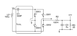
- Fig. 1 is a circuit diagram which shows a configuration of a wireless power supply system according to an embodiment
- Fig. 2A is a circuit diagram showing the operation of the wireless power receiving apparatus shown in Fig. 1
- Fig. 2B is a circuit diagram showing the operation of the wireless power receiving apparatus shown in Fig. 1
- Fig. 3 is a waveform diagram which shows the operation of the wireless power receiving apparatus shown in Fig. 1
- Fig. 4 is a waveform diagram which shows the operation of a synchronous rectifier circuit as a comparison technique
- Fig. 1 is a circuit diagram which shows a configuration of a wireless power supply system according to an embodiment
- Fig. 2A is a circuit diagram showing the operation of the wireless power receiving apparatus shown in Fig. 1
- Fig. 2B is a circuit diagram showing the operation of the wireless power receiving apparatus shown in Fig. 1
- Fig. 3 is a waveform diagram which shows the operation of the wireless power receiving apparatus shown in Fig. 1
- Fig. 4 is a
- FIG. 5 is a circuit diagram which shows a configuration of a wireless power receiving apparatus according to a first modification
- Fig. 6 is a circuit diagram which shows a configuration of a wireless power receiving apparatus according to a second modification
- Fig. 7 is an equivalent circuit diagram which shows a wireless power supply system shown in Fig. 1
- Fig. 8 is a time chart which shows the operation of a wireless power supply system according to a third modification
- Fig. 9 is a circuit diagram which shows a configuration of a wireless power receiving apparatus according to a fourth modification.
- the state represented by the phrase “the member A is connected to the member B” includes a state in which the member A is indirectly connected to the member B via another member that does not affect the electric connection therebetween, in addition to a state in which the member A is physically and directly connected to the member B.
- the state represented by the phrase “the member C is provided between the member A and the member B” includes a state in which the member A is indirectly connected to the member C, or the member B is indirectly connected to the member C via another member that does not affect the electric connection therebetween, in addition to a state in which the member A is directly connected to the member C, or the member B is directly connected to the member C.
- Fig. 1 is a circuit diagram which shows a configuration of a wireless power supply system 100 according to an embodiment.
- circuit constants are shown for exemplary purposes. However, such circuit constants are not intended to limit the present invention.
- the wireless power supply system 100 includes a wireless power supply apparatus 200 and a wireless power receiving apparatus 300. First, description will be made regarding the configuration of the wireless power supply apparatus 200.
- the wireless power supply apparatus 200 transmits an electric power signal to the wireless power receiving apparatus 300.
- an electric power signal S1 the wireless power supply system 100 uses the near-field component (electric field, magnetic field, or electromagnetic field) of electromagnetic waves that has not become radio waves.
- the wireless power supply apparatus 200 includes an AC power supply 10, a transmission coil L1, and a capacitor C2.
- the AC power supply 10 generates an electric signal S2 having a predetermined frequency, or subjected to frequency-modulation, phase-modulation, amplitude-modulation, or the like.
- the electric signal S2 is an AC signal having a constant frequency.
- the frequency of the electric signal S2 is selected from a range between several hundred KHz and several MHz.
- the transmission coil L1 is an antenna configured to emit the electric signal S2 generated by the AC power supply 10, as a near-field signal (electric power signal) including any one of an electric field, magnetic field, or electromagnetic field.
- the transmission capacitor C2 is arranged in series with the transmission coil L1.
- the resistor R1 represents the resistance component that is in series with the transmission coil L1.
- the above is the configuration of the wireless power supply apparatus 200. Next, description will be made regarding the configuration of the wireless power receiving apparatus 300.
- the wireless power receiving apparatus 300 receives the electric power signal S1 transmitted from the wireless power supply apparatus 200.
- the reception coil 20 receives the electric power signal S1 from the transmission coil L1.
- An induced current (resonant current) I COIL that corresponds to the electric power signal S1 flows through the reception coil L2.
- the wireless power receiving apparatus 300 acquires electric power via the induced current thus generated.
- the wireless power receiving apparatus 300 includes a reception coil L2, a resonance capacitor C1, an H-bridge circuit 12, a control unit 14 and a power storage capacitor C3. Together with the reception coil L2, the resonance capacitor C1 forms a resonance circuit.
- the H-bridge circuit 12 includes a first switch SW1 through a fourth switch SW4.
- the first switch SW1 and the second switch SW2 are sequentially connected in series so as to form a closed loop including the reception coil L2 and the resonance capacitor C1.
- a connection node N1 that connects the first switch SW1 and the second switch SW2 is connected to a second terminal of the power storage capacitor C3.
- a loss resistance R2 represents power loss that occurs in the wireless power receiving apparatus 300.
- a load resistor R3 represents a load driven by the electric power stored in the power storage capacitor C3, and does not represents a resistor arranged as a circuit component.
- a voltage V PWR that develops at the power storage capacitor C3 is supplied to the load resistance R3.
- the third switch SW3 and the fourth switch SW4 are sequentially arranged in series so as to form a path that is parallel to a path that includes the first switch SW1 and the second switch SW2.
- a connection node N2 that connects the third switch SW3 and the fourth switch SW4 is grounded, and has a fixed electric potential.
- the load resistor R3 may be controlled such that the voltage V PWR that develops at the power storage capacitor C3 becomes the optimum value for increasing the Q value.
- the first switch SW1 through the fourth switch SW4 are each configured as a MOSFET (Metal Oxide Semiconductor Field Effect Transistor), a bipolar transistor, or an IGBT (Insulated Gate Bipolar Transistor), or the like.
- MOSFET Metal Oxide Semiconductor Field Effect Transistor
- bipolar transistor a bipolar transistor
- IGBT Insulated Gate Bipolar Transistor
- a control unit 14 controls the first switch SW1 through the fourth switch SW4.
- the control unit 14 is configured to be capable of switching the state between a first state phi1 and a second state phi2.
- a word "phi” represents Greek alphabet "phi”.
- the first switch SW1 and the fourth switch SW4 are on, and the second switch SW2 and the third switch SW3 are off.
- the second switch SW2 and the third switch SW3 are on.
- the induced current I COIL that develops at the reception coil L2 has an AC waveform.
- the control unit 14 adjusts a switching timing (phase) at which the state is switched between the first state phi1 and the second state phi2, such that the amplitude of the induced current I COIL approaches the maximum value.
- Figs. 2A and 2B are circuit diagrams each showing the operation of the wireless power receiving apparatus 300 shown in Fig. 1.
- Fig. 2A shows the state of each switch and the current in the first state phi1
- Fig. 2B shows the state of each switch and the current in the second state phi2.
- Fig. 3 is a waveform diagram which shows the operation of the wireless power receiving apparatus 300 shown in Fig. 1. From the top and in the following order, Fig.
- FIG 3 shows the voltage V PWR that develops at the power storage capacitor C3, a current I C3 that flows into the power storage capacitor C3, the states of the second switch SW2 and the third switch SW3, the states of the first switch SW1 and the fourth switch SW4, and the induced current I COIL that develops at the reception coil L2.
- the states of the second switch SW2 and the third switch SW3 each correspond to the fully-on state when the voltage is +1 V, and correspond to the off state when the voltage is 0 V.
- the states of the first switch SW1 and the fourth switch SW4 each correspond to the fully-on state when the voltage is -1 V, and correspond to the off state when the voltage is 0 V.
- the voltage level which indicates the state of each switch is determined for convenience. The waveform is shown with the direction of the arrow shown in Fig. 1 as the positive direction.
- the AC electric power signal S1 is transmitted from the wireless power supply apparatus 200 shown in Fig. 1.
- the induced current I COIL which is an AC current, flows through the reception coil L2 according to the electric power signal S1.
- the control unit 14 controls the on/off state of each of the first switch SW1 through the fourth switch SW4 in synchronization with the electric power signal S1.
- the current I C3 flows from the ground terminal via the fourth switch SW4, the reception coil L2, the resonance capacitor C1, and the first switch SW1, as shown in Fig. 2A.
- the current I C3 flows from the ground terminal via the third switch SW3, the reception coil L2, the resonance capacitor C1, and the second switch SW2, as shown in Fig. 2B.
- the control unit 14 may monitor the induced current I COIL or the electric power supplied to the load resistor R3, and may optimize the switching timing (phase) at which the H-bridge circuit 12 is switched such that the amplitude thereof approaches the maximum value.
- such a power storage capacitor C3 can be used as a driving voltage source for the resonance circuit.
- a phase shifted by 90 degrees with respect to the zero-crossing point of the induced current (resonance current) I COIL such an arrangement is capable of compensating for the loss due to the resistance component of the reception coil L2 and so forth by means of the power storage capacitor C3 functioning as a power supply.
- the Q value of the resonance circuit is inversely proportional to the resistance R.
- the resistance R can be regarded as zero, thereby providing a circuit equivalent to a resonance circuit having an infinite Q value.
- Fig. 7 is an equivalent circuit diagram showing the wireless power supply system 100 shown in Fig. 1.
- the transmission coil L1 and the reception coil L2, which are coupled with a coupling coefficient k can be regarded as a T-shaped circuit 20 including inductors L5 through L7.
- the inductances of the inductors L5 and L6 are each represented by L x (1 - k)
- the inductance of L6 is represented by L x k.
- optimization of the switching timing at which the H-bridge circuit 12 is switched between the first state phi1 and the second state phi2 is equivalent to optimization of impedance matching between the AC power supply 10 and the load resistor R3. That is to say, the H-bridge circuit 12 can be regarded as a switch-mode impedance matching circuit. If the output impedance of the AC power supply 10 or the coupling coefficient k changes, the impedance matching conditions also change. The phase of the switching operation of the H-bridge circuit 12 is controlled so as to provide optimum impedance matching.
- the resonance capacitor C1 or C2 is configured as a variable capacitor, and this variable capacitor is mechanically controlled by means of a motor so as to provide such impedance matching.
- this variable capacitor is mechanically controlled by means of a motor so as to provide such impedance matching.
- by controlling the switching state of the H-bridge circuit 12 such an arrangement provides the impedance matching electrically instead of mechanically.
- the present embodiment provides high-speed impedance matching as compared to such a conventional arrangement.
- the present arrangement provides a highly efficient power supply even if the wireless power receiving apparatus 300 moves, or even if the power supply state of the wireless power supply apparatus 200 is switched at a high speed.
- the wireless power receiving apparatus 300 having a high Q value provides high-efficiency electric power transmission even if the coupling coefficient k between the transmission coil L1 and the reception coil L2 is low, i.e., even if there is a great distance between the wireless power receiving apparatus 300 and the wireless power supply apparatus 200.
- each of the first switch SW1 through the fourth switch SW4 is not restricted to such an arrangement described with reference to Fig. 3.
- Such an arrangement is capable of controlling the Q value of the resonance circuit.
- such an arrangement may intentionally shift the on/off switching timing from that shown in Fig. 3.
- the H-bridge circuit 12 configured to raise the Q value also functions as a rectifier circuit.
- the H-bridge circuit 12 configured to raise the Q value also functions as a rectifier circuit.
- Fig. 4 is a waveform diagram which shows the operation of a synchronous rectifier circuit as a comparison technique.
- the state is switched between the first state phi1 and the second state phi2 when a zero-crossing point occurs in the resonance current I COIL .
- the current I C3 that flows into the power storage capacitor C3 has a waveform that has been subjected to full-wave rectification.
- voltage loss does not occur in this rectification.
- Such a synchronous rectifier circuit cannot compensate for the loss that occurs in the resonance circuit. Accordingly, such an arrangement does not provide an improved Q value.
- Fig. 5 is a circuit diagram which shows a configuration of a wireless power receiving apparatus 300a according to a first modification. It should be noted that a part of the circuit components that overlaps those shown in Fig. 1 are not shown.
- the point of difference between the wireless power receiving apparatus 300a shown in Fig. 5 and the wireless power receiving apparatus 300 shown in Fig. 1 is the position of the load. Specifically, in Fig. 5, the resistor R6 functions as a load, instead of the resistor R3.
- the resistor R3 arranged in parallel with the power storage capacitor C3 has a negligible effect.
- the wireless power receiving apparatus 300a shown in Fig. 5 includes an auxiliary coil L3, a rectifier circuit 16, and an inductor L4, in addition to the wireless power receiving apparatus 300 shown in Fig. 1.
- the auxiliary coil L3 is densely coupled with the reception coil L2.
- the rectifier circuit 16 performs full-wave rectification of a current I L3 that flows through the auxiliary coil L3.
- the inductor L4 is arranged on the output side of the rectifier circuit 16 in series with the load resistor R6.
- the Q value of the resonance circuit comprising the reception coil L2 and the resonance capacitor C1 is raised by the Q value amplifier circuit including the H-bridge circuit 12 and the power storage capacitor C3.
- the Q value amplifier circuit including the H-bridge circuit 12 and the power storage capacitor C3.
- Fig. 6 is a circuit diagram which shows a configuration of a wireless power receiving apparatus 300b according to a second modification.
- the wireless power receiving apparatus 300b includes an auxiliary coil L3 densely coupled with the reception coil L2.
- an H-bridge circuit 12b is connected to the auxiliary coil L3, instead of the reception coil L2.
- An inductor L4 and a resistor R5 connected in parallel are arranged between the H-bridge circuit 12b and the power storage capacitor C3.
- the rectifier circuit 16b performs full-wave rectification of the current that flows through the resonance circuit including the reception coil L2 and the resonance capacitor C1.
- the power storage capacitor C4 is arranged on the output side of the rectifier circuit 16b, and is configured to smooth the current thus subjected to full-wave rectification by the rectifier circuit 16b.
- the voltage that develops at the power storage capacitor C4 is supplied to the load resistor R6.
- a Q value amplifier circuit comprising the H-bridge circuit 12b and the power storage capacitor C3 is capable of raising the Q value of the resonance circuit that includes the reception coil L2 and the resonance capacitor C1.
- a Q value amplifier circuit comprising the H-bridge circuit 12b and the power storage capacitor C3 is capable of raising the Q value of the resonance circuit that includes the reception coil L2 and the resonance capacitor C1.
- the control unit 14 is capable of switching the state to a third state f3 in which all of the first switch SW1 through the fourth switch SW4 are turned off, in addition to the first state phi1 and the second state phi2.
- the control unit 14 provides the third state f3 as an intermediate state in at least one of the transitions from the first state phi1 to the second state phi2 or from the second state phi2 to the first state phi1, so as to adjust the length of the period of time for the third state f3 (which will also be referred to as the "dead time Td") such that the amplitude of the induced current I COIL that flows through the reception coil L2 approaches the maximum value.
- Fig. 8 is a time chart which shows the operation of the wireless power supply system 100 according to a third modification.
- the resonance frequency of the resonance circuit that comprises the reception coil L2, the resonance capacitor C1, and the H-bridge circuit 12, does not necessarily match the frequency of the electric power signal S1 generated by the wireless power supply apparatus 200.
- such an arrangement allows the induced current I COIL that flows in the first state phi1 and in the second state phi2 to partially resonate with the resonance circuit included in the wireless power receiving apparatus 300. That is to say, such an arrangement is capable of tuning the resonance frequency of the wireless power supply apparatus 200 to the frequency of the electric power signal S1, thereby improving the power supply efficiency.
- Fig. 9 is a circuit diagram which shows a configuration of a wireless power receiving apparatus 300c according to a fourth modification.
- the wireless power receiving apparatus 300c shown in Fig. 9 has a configuration obtained by replacing the H-bridge circuit 12b included in the wireless power receiving apparatus 300b shown in Fig. 6 with a half-bridge circuit 12c.
- the half-bridge circuit 12c includes a fifth switch SW5 and a sixth switch SW6.
- the fifth switch SW5 is connected to the power storage capacitor C3 and the auxiliary coil L3 so as to form a closed loop.
- the sixth switch SW6 is arranged between both terminals of the auxiliary coil L3.
- switch-mode impedance matching circuit 12 is provided only on the wireless power receiving apparatus 300 side.
- a switch-mode impedance matching circuit such as a half-bridge circuit and an H-bridge circuit is preferably also provided on the wireless power supply apparatus 200 side: specifically, to the output stage of the AC power supply 10.
Landscapes
- Engineering & Computer Science (AREA)
- Computer Networks & Wireless Communication (AREA)
- Power Engineering (AREA)
- Charge And Discharge Circuits For Batteries Or The Like (AREA)
- Near-Field Transmission Systems (AREA)
Abstract
Description
In a case in which electric power is to be supplied over a relatively long range of several meters or more, the electromagnetic wave reception method is employed. The electromagnetic wave reception method allows electric power of several watts or less to be transmitted in a band between medium waves and microwaves. However, the power use efficiency thereof is small. The electric field/magnetic field resonance method has been receiving attention as a method for supplying electric power with relatively high efficiency at a middle range on the order of several meters (see Non-patent document 1).
Moreover, this summary of the invention does not necessarily describe all necessary features so that the invention may also be a sub-combination of these described features.
Similarly, the state represented by the phrase "the member C is provided between the member A and the member B" includes a state in which the member A is indirectly connected to the member C, or the member B is indirectly connected to the member C via another member that does not affect the electric connection therebetween, in addition to a state in which the member A is directly connected to the member C, or the member B is directly connected to the member C.
Specifically, the
Claims (9)
- A wireless power receiving apparatus configured to receive an electric power signal including any one of an electric field, a magnetic field, and an electromagnetic field, transmitted from a wireless power supply apparatus, the power receiving apparatus comprising:
a reception coil configured to receive the electric power signal;
a capacitor arranged such that a first terminal thereof is set to a fixed electric potential;
a first switch and a second switch sequentially connected in series so as to form a closed loop together with the reception coil, and arranged such that a connection node that connects the first and second switches is connected to a second terminal of the capacitor;
a third switch and a fourth switch sequentially arranged in series so as to form a path arranged in parallel with a path comprising the first and second switches, and arranged such that a connection node that connects the third and fourth switches is set to a fixed electric potential; and
a control unit configured to control the first switch through the fourth switch. - A wireless power receiving apparatus according to Claim 1, wherein the control unit is configured to be capable of switching states between a first state in which the first switch and the fourth switch are on and the second switch and the third switch are off, and a second state in which the first switch and the fourth switch are off and the second switch and the third switch are on.
- A wireless power receiving apparatus according to Claim 2, wherein the control unit controls a switching timing at which the state is switched between the first state and the second state such that the amplitude of a current that flows through the reception coil approaches a maximum value.
- A wireless power receiving apparatus according to Claim 2, wherein the control unit is configured to have a third switchable state in which all of the first switch through the fourth switch are off, in addition to the first state and the second state.
- A wireless power receiving apparatus according to Claim 4, wherein the length of the third state is controlled such that the amplitude of a current that flows through the reception coil approaches a maximum value.
- A wireless power receiving apparatus according to any one of Claim 1 through Claim 5, wherein the first and second switches are arranged to form a closed loop together with an auxiliary coil densely coupled with the reception coil, instead of with the reception coil.
- A wireless power receiving apparatus configured to receive any one of an electric field, a magnetic field, an electromagnetic field, transmitted from a power receiving apparatus, the wireless power receiving apparatus comprising:
a reception coil configured to receive the electric power signal;
a capacitor arranged such that a first terminal thereof is set to a fixed electric potential; and
an impedance matching circuit comprising at least one switch, and configured to be capable of changing the ON/OFF timing of at least the one switch, and arranged between the capacitor and the reception coil. - A wireless power receiving apparatus according to Claim 7, wherein the impedance matching circuit is arranged between the capacitor and an auxiliary coil densely coupled with the reception coil, instead of the reception coil.
- A wireless power supply system comprising:
a wireless power supply apparatus configured to transmit an electric power signal including any one of an electric field, a magnetic field, and an electromagnetic field; and
a wireless power receiving apparatus according to any one of Claim 1 through Claim 8.
Priority Applications (3)
| Application Number | Priority Date | Filing Date | Title |
|---|---|---|---|
| CN2011800173274A CN102823148A (en) | 2010-04-02 | 2011-03-31 | Wireless power receiving apparatus capable of providing high q value |
| JP2012544366A JP5462953B2 (en) | 2010-04-02 | 2011-03-31 | Wireless power receiving apparatus and wireless power feeding system |
| KR1020127028913A KR20130043629A (en) | 2010-04-02 | 2011-03-31 | Wireless power receiving apparatus capable of providing a high q value |
Applications Claiming Priority (4)
| Application Number | Priority Date | Filing Date | Title |
|---|---|---|---|
| US32054810P | 2010-04-02 | 2010-04-02 | |
| US61/320,548 | 2010-04-02 | ||
| US13/070,674 US8791601B2 (en) | 2010-04-02 | 2011-03-24 | Wireless power receiving apparatus and wireless power supply system |
| US13/070,674 | 2011-03-24 |
Publications (1)
| Publication Number | Publication Date |
|---|---|
| WO2011122048A1 true WO2011122048A1 (en) | 2011-10-06 |
Family
ID=44708773
Family Applications (1)
| Application Number | Title | Priority Date | Filing Date |
|---|---|---|---|
| PCT/JP2011/001967 WO2011122048A1 (en) | 2010-04-02 | 2011-03-31 | Wireless power receiving apparatus capable of providing a high q value |
Country Status (6)
| Country | Link |
|---|---|
| US (1) | US8791601B2 (en) |
| JP (1) | JP5462953B2 (en) |
| KR (1) | KR20130043629A (en) |
| CN (1) | CN102823148A (en) |
| TW (1) | TWI435509B (en) |
| WO (1) | WO2011122048A1 (en) |
Cited By (3)
| Publication number | Priority date | Publication date | Assignee | Title |
|---|---|---|---|---|
| JP2013187962A (en) * | 2012-03-06 | 2013-09-19 | Advantest Corp | Wireless power reception device, wireless power supply device, and wireless power transmission system |
| JP2014103778A (en) * | 2012-11-20 | 2014-06-05 | Mitsubishi Electric Engineering Co Ltd | Transmission system by wireless power transmission and transmission side transmission equipment |
| JP2014135785A (en) * | 2012-11-20 | 2014-07-24 | Mitsubishi Electric Engineering Co Ltd | Transmission system and receiving side transmission apparatus by radio power transmission |
Families Citing this family (52)
| Publication number | Priority date | Publication date | Assignee | Title |
|---|---|---|---|---|
| US20120068548A1 (en) * | 2010-09-16 | 2012-03-22 | Advantest Corporation | Wireless power supply apparatus |
| US9203380B2 (en) * | 2010-12-29 | 2015-12-01 | National Semiconductor Corporation | Resonance tuning |
| US10312748B2 (en) | 2011-02-01 | 2019-06-04 | Fu Da Tong Techology Co., Ltd. | Signal analysis method and circuit |
| US10951063B2 (en) | 2011-02-01 | 2021-03-16 | Fu Da Tong Technology Co., Ltd. | Supplying-end module of induction type power supply system and signal detection method thereof |
| TWI663806B (en) * | 2018-02-12 | 2019-06-21 | 富達通科技股份有限公司 | Supplying-end module of induction type power supply system and signal detection method using the same |
| US10289142B2 (en) | 2011-02-01 | 2019-05-14 | Fu Da Tong Technology Co., Ltd. | Induction type power supply system and intruding metal detection method thereof |
| US11128180B2 (en) | 2011-02-01 | 2021-09-21 | Fu Da Tong Technology Co., Ltd. | Method and supplying-end module for detecting receiving-end module |
| US10673287B2 (en) | 2011-02-01 | 2020-06-02 | Fu Da Tong Technology Co., Ltd. | Method and supplying-end module for detecting receiving-end module |
| US10038338B2 (en) | 2011-02-01 | 2018-07-31 | Fu Da Tong Technology Co., Ltd. | Signal modulation method and signal rectification and modulation device |
| US10574095B2 (en) | 2011-02-01 | 2020-02-25 | Fu Da Tong Technology Co., Ltd. | Decoding method for signal processing circuit and signal processing circuit using the same |
| KR101855432B1 (en) * | 2011-09-07 | 2018-06-14 | 솔라스 파워 인크. | Wireless electric field power transmission system and method |
| CN104054229B (en) * | 2012-01-06 | 2018-01-23 | 捷通国际有限公司 | Wireless power receiver system |
| KR102065021B1 (en) | 2012-01-24 | 2020-01-10 | 필립스 아이피 벤쳐스 비.브이. | Wireless power control system |
| JP5620424B2 (en) * | 2012-03-06 | 2014-11-05 | 株式会社東芝 | Wireless power receiving apparatus and wireless power transmitting apparatus |
| WO2014018969A2 (en) | 2012-07-27 | 2014-01-30 | Thoratec Corporation | Resonant power transfer system and method of estimating system state |
| US10291067B2 (en) | 2012-07-27 | 2019-05-14 | Tc1 Llc | Computer modeling for resonant power transfer systems |
| EP4257174A3 (en) | 2012-07-27 | 2023-12-27 | Tc1 Llc | Thermal management for implantable wireless power transfer systems |
| US10383990B2 (en) | 2012-07-27 | 2019-08-20 | Tc1 Llc | Variable capacitor for resonant power transfer systems |
| WO2014018971A1 (en) | 2012-07-27 | 2014-01-30 | Thoratec Corporation | Resonant power transfer systems with protective algorithm |
| US9287040B2 (en) | 2012-07-27 | 2016-03-15 | Thoratec Corporation | Self-tuning resonant power transfer systems |
| WO2014018974A1 (en) | 2012-07-27 | 2014-01-30 | Thoratec Corporation | Magnetic power transmission utilizing phased transmitter coil arrays and phased receiver coil arrays |
| WO2014018973A1 (en) | 2012-07-27 | 2014-01-30 | Thoratec Corporation | Resonant power transmission coils and systems |
| JP6382818B2 (en) | 2012-09-11 | 2018-08-29 | フィリップス アイピー ベンチャーズ ビー ヴィ | Wireless power control |
| US9998180B2 (en) * | 2013-03-13 | 2018-06-12 | Integrated Device Technology, Inc. | Apparatuses and related methods for modulating power of a wireless power receiver |
| WO2014145895A1 (en) | 2013-03-15 | 2014-09-18 | Thoratec Corporation | Malleable tets coil with improved anatomical fit |
| WO2014145664A1 (en) | 2013-03-15 | 2014-09-18 | Thoratec Corporation | Integrated implantable tets housing including fins and coil loops |
| JP6208503B2 (en) * | 2013-09-11 | 2017-10-04 | ローム株式会社 | Wireless power receiving apparatus, control circuit and control method thereof |
| US9735584B2 (en) * | 2013-10-17 | 2017-08-15 | Access Business Group International Llc | Wireless power communication |
| US10615642B2 (en) | 2013-11-11 | 2020-04-07 | Tc1 Llc | Resonant power transfer systems with communications |
| EP3072211A4 (en) | 2013-11-11 | 2017-07-05 | Thoratec Corporation | Resonant power transfer systems with communications |
| EP3069358B1 (en) | 2013-11-11 | 2019-06-12 | Tc1 Llc | Hinged resonant power transfer coil |
| US10610692B2 (en) | 2014-03-06 | 2020-04-07 | Tc1 Llc | Electrical connectors for implantable devices |
| US9634514B2 (en) | 2014-05-30 | 2017-04-25 | Infineon Technologies Austria Ag | Single stage rectification and regulation for wireless charging systems |
| US9641364B2 (en) * | 2014-05-30 | 2017-05-02 | Nxp B.V. | Communication circuit and approach with modulation |
| JP2017520231A (en) | 2014-06-26 | 2017-07-20 | ソレース・パワー・インコーポレイテッド | Wireless electric field power transmission system, transmitter and receiver therefor, and method for wirelessly transmitting power |
| CN111509868B (en) | 2014-09-05 | 2023-11-24 | 索雷斯能源公司 | Wireless power transfer system and vehicle thereof |
| US10186760B2 (en) | 2014-09-22 | 2019-01-22 | Tc1 Llc | Antenna designs for communication between a wirelessly powered implant to an external device outside the body |
| US9583874B2 (en) | 2014-10-06 | 2017-02-28 | Thoratec Corporation | Multiaxial connector for implantable devices |
| WO2016072865A1 (en) | 2014-11-05 | 2016-05-12 | Powerbyproxi Limited | An inductive power receiver |
| US9762135B2 (en) | 2014-11-05 | 2017-09-12 | Infineon Technologies Austria Ag | Secondary side control of resonant DC/DC converters |
| WO2016093057A1 (en) * | 2014-12-08 | 2016-06-16 | ソニー株式会社 | Antenna and communication apparatus |
| US10148126B2 (en) | 2015-08-31 | 2018-12-04 | Tc1 Llc | Wireless energy transfer system and wearables |
| WO2017062552A1 (en) | 2015-10-07 | 2017-04-13 | Tc1 Llc | Resonant power transfer systems having efficiency optimization based on receiver impedance |
| JP6538628B2 (en) * | 2016-09-05 | 2019-07-03 | 株式会社東芝 | Filter circuit and wireless power transmission system |
| TWI604678B (en) * | 2016-09-07 | 2017-11-01 | 國立暨南國際大學 | Radio transmission system |
| EP3497775B1 (en) | 2016-09-21 | 2022-07-13 | Tc1 Llc | Systems and methods for locating implanted wireless power transmission devices |
| US11197990B2 (en) | 2017-01-18 | 2021-12-14 | Tc1 Llc | Systems and methods for transcutaneous power transfer using microneedles |
| WO2019135890A1 (en) | 2018-01-04 | 2019-07-11 | Tc1 Llc | Systems and methods for elastic wireless power transmission devices |
| JP6638793B2 (en) * | 2018-10-24 | 2020-01-29 | 株式会社Soken | Wireless power supply |
| US20230013502A1 (en) | 2019-02-21 | 2023-01-19 | Raisontech Inc. | Wireless power feeding system, and power receiver having circular, spherical, or polyhedral shape |
| EP3952002A4 (en) | 2019-03-28 | 2023-04-19 | Aoi Japan Co., Ltd. | Wireless power feeding system having battery mounted device engaged with power receiving device with light unit mounted |
| JP7395879B2 (en) * | 2019-08-28 | 2023-12-12 | オムロン株式会社 | Contactless power supply device and power transmission device |
Citations (2)
| Publication number | Priority date | Publication date | Assignee | Title |
|---|---|---|---|---|
| WO2001018936A1 (en) * | 1999-09-09 | 2001-03-15 | Auckland Uniservices Limited | Control of series-resonant inductive pickups |
| US20060082324A1 (en) * | 2003-04-09 | 2006-04-20 | Boys John T | Decoupling circuits |
Family Cites Families (12)
| Publication number | Priority date | Publication date | Assignee | Title |
|---|---|---|---|---|
| CA1239986A (en) | 1985-02-06 | 1988-08-02 | Reliance Electric Company | Control of a series resonant converter |
| JPH03139168A (en) | 1989-10-24 | 1991-06-13 | Hitachi Metals Ltd | Series resonance converter |
| EP0640254B1 (en) | 1992-05-10 | 2001-08-01 | Auckland Uniservices Limited | A non-contact power distribution system |
| JP3139168B2 (en) | 1992-10-07 | 2001-02-26 | 株式会社豊田自動織機製作所 | Cloth tension applying method in cross roll changing device |
| JPH07227003A (en) | 1993-12-15 | 1995-08-22 | Fuji Electric Co Ltd | Non-contacting power feeding device for traveling object |
| JP2001297862A (en) | 2000-04-14 | 2001-10-26 | Fuji Electric Co Ltd | Induction heating power supply |
| US6538909B2 (en) * | 2001-12-13 | 2003-03-25 | Enova Systems | Universal high efficiency power converter |
| KR100446931B1 (en) | 2002-04-30 | 2004-09-04 | 주식회사 두노시스템 | Adapter for using Power Line Communication |
| US7221977B1 (en) * | 2004-06-25 | 2007-05-22 | Pacesetter, Inc. | Method and apparatus for measuring battery depletion in implantable medical devices |
| JP4258505B2 (en) | 2005-08-25 | 2009-04-30 | パナソニック電工株式会社 | Power supply system |
| US11522389B2 (en) * | 2008-09-11 | 2022-12-06 | Auckland Uniservices Limited | Inductively coupled AC power transfer |
| US8923015B2 (en) * | 2008-11-26 | 2014-12-30 | Auckland Uniservices Limited | Primary-side power control for inductive power transfer |
-
2011
- 2011-03-24 US US13/070,674 patent/US8791601B2/en active Active
- 2011-03-31 JP JP2012544366A patent/JP5462953B2/en active Active
- 2011-03-31 KR KR1020127028913A patent/KR20130043629A/en not_active Application Discontinuation
- 2011-03-31 WO PCT/JP2011/001967 patent/WO2011122048A1/en active Application Filing
- 2011-03-31 CN CN2011800173274A patent/CN102823148A/en active Pending
- 2011-04-01 TW TW100111551A patent/TWI435509B/en not_active IP Right Cessation
Patent Citations (2)
| Publication number | Priority date | Publication date | Assignee | Title |
|---|---|---|---|---|
| WO2001018936A1 (en) * | 1999-09-09 | 2001-03-15 | Auckland Uniservices Limited | Control of series-resonant inductive pickups |
| US20060082324A1 (en) * | 2003-04-09 | 2006-04-20 | Boys John T | Decoupling circuits |
Non-Patent Citations (1)
| Title |
|---|
| A. KARALIS, J.D. JOANNOPOULOS, M. SOLJACIC: "Efficient wireless non-radiative mid-range energy transfer", ANNALS OF PHYSICS, vol. 323, January 2008 (2008-01-01), pages 34 - 48 |
Cited By (5)
| Publication number | Priority date | Publication date | Assignee | Title |
|---|---|---|---|---|
| JP2013187962A (en) * | 2012-03-06 | 2013-09-19 | Advantest Corp | Wireless power reception device, wireless power supply device, and wireless power transmission system |
| TWI565182B (en) * | 2012-03-06 | 2017-01-01 | 愛德萬測試股份有限公司 | Wireless power receiving and supplying apparatus, and wireless power supplying system |
| US9742201B2 (en) | 2012-03-06 | 2017-08-22 | Advantest Corporation | Wireless power receiving apparatus |
| JP2014103778A (en) * | 2012-11-20 | 2014-06-05 | Mitsubishi Electric Engineering Co Ltd | Transmission system by wireless power transmission and transmission side transmission equipment |
| JP2014135785A (en) * | 2012-11-20 | 2014-07-24 | Mitsubishi Electric Engineering Co Ltd | Transmission system and receiving side transmission apparatus by radio power transmission |
Also Published As
| Publication number | Publication date |
|---|---|
| US8791601B2 (en) | 2014-07-29 |
| JP2013524743A (en) | 2013-06-17 |
| TWI435509B (en) | 2014-04-21 |
| US20110241436A1 (en) | 2011-10-06 |
| TW201210168A (en) | 2012-03-01 |
| KR20130043629A (en) | 2013-04-30 |
| CN102823148A (en) | 2012-12-12 |
| JP5462953B2 (en) | 2014-04-02 |
Similar Documents
| Publication | Publication Date | Title |
|---|---|---|
| US8791601B2 (en) | Wireless power receiving apparatus and wireless power supply system | |
| US20120068548A1 (en) | Wireless power supply apparatus | |
| US10243408B2 (en) | Wireless power receiver | |
| US9589721B2 (en) | Wireless power transmitter and wireless power receiver | |
| US10566840B2 (en) | Wireless power feeding system | |
| US9893534B2 (en) | Relay device of wireless power transmission system | |
| US9071063B2 (en) | Wireless power receiving apparatus | |
| US20190304679A1 (en) | Coupled inductor system having multi-tap coil | |
| US20140183972A1 (en) | Wireless power transmitter and wireless power receiver | |
| US9882550B2 (en) | Wireless power transmitting apparatus and wireless power supply system | |
| US20110285211A1 (en) | Wireless power supply system | |
| US9871413B2 (en) | Wireless power receiving apparatus | |
| JP5764032B2 (en) | Wireless power feeding device, power receiving device and power feeding system | |
| US20110316347A1 (en) | Wireless power receiving apparatus | |
| US20190067997A1 (en) | Wireless power transmitting apparatus and method thereof | |
| US20140132078A1 (en) | Wireless power transmitter | |
| KR20170025517A (en) | Device and Method of using Piezoelectric Transformer for Wireless Power Transmission |
Legal Events
| Date | Code | Title | Description |
|---|---|---|---|
| WWE | Wipo information: entry into national phase |
Ref document number: 201180017327.4 Country of ref document: CN |
|
| 121 | Ep: the epo has been informed by wipo that ep was designated in this application |
Ref document number: 11716665 Country of ref document: EP Kind code of ref document: A1 |
|
| WWE | Wipo information: entry into national phase |
Ref document number: 2012544366 Country of ref document: JP |
|
| NENP | Non-entry into the national phase |
Ref country code: DE |
|
| ENP | Entry into the national phase |
Ref document number: 20127028913 Country of ref document: KR Kind code of ref document: A |
|
| 122 | Ep: pct application non-entry in european phase |
Ref document number: 11716665 Country of ref document: EP Kind code of ref document: A1 |