WO2011108148A1 - 記録媒体、再生及び記録方法、再生及び記録装置 - Google Patents
記録媒体、再生及び記録方法、再生及び記録装置 Download PDFInfo
- Publication number
- WO2011108148A1 WO2011108148A1 PCT/JP2010/070010 JP2010070010W WO2011108148A1 WO 2011108148 A1 WO2011108148 A1 WO 2011108148A1 JP 2010070010 W JP2010070010 W JP 2010070010W WO 2011108148 A1 WO2011108148 A1 WO 2011108148A1
- Authority
- WO
- WIPO (PCT)
- Prior art keywords
- address
- data
- recording
- bits
- recording medium
- Prior art date
- Legal status (The legal status is an assumption and is not a legal conclusion. Google has not performed a legal analysis and makes no representation as to the accuracy of the status listed.)
- Ceased
Links
Images






Classifications
-
- G—PHYSICS
- G11—INFORMATION STORAGE
- G11B—INFORMATION STORAGE BASED ON RELATIVE MOVEMENT BETWEEN RECORD CARRIER AND TRANSDUCER
- G11B20/00—Signal processing not specific to the method of recording or reproducing; Circuits therefor
- G11B20/10—Digital recording or reproducing
- G11B20/12—Formatting, e.g. arrangement of data block or words on the record carriers
- G11B20/1217—Formatting, e.g. arrangement of data block or words on the record carriers on discs
-
- G—PHYSICS
- G11—INFORMATION STORAGE
- G11B—INFORMATION STORAGE BASED ON RELATIVE MOVEMENT BETWEEN RECORD CARRIER AND TRANSDUCER
- G11B27/00—Editing; Indexing; Addressing; Timing or synchronising; Monitoring; Measuring tape travel
- G11B27/02—Editing, e.g. varying the order of information signals recorded on, or reproduced from, record carriers
- G11B27/031—Electronic editing of digitised analogue information signals, e.g. audio or video signals
- G11B27/034—Electronic editing of digitised analogue information signals, e.g. audio or video signals on discs
-
- G—PHYSICS
- G11—INFORMATION STORAGE
- G11B—INFORMATION STORAGE BASED ON RELATIVE MOVEMENT BETWEEN RECORD CARRIER AND TRANSDUCER
- G11B27/00—Editing; Indexing; Addressing; Timing or synchronising; Monitoring; Measuring tape travel
- G11B27/10—Indexing; Addressing; Timing or synchronising; Measuring tape travel
- G11B27/19—Indexing; Addressing; Timing or synchronising; Measuring tape travel by using information detectable on the record carrier
- G11B27/24—Indexing; Addressing; Timing or synchronising; Measuring tape travel by using information detectable on the record carrier by sensing features on the record carrier other than the transducing track ; sensing signals or marks recorded by another method than the main recording
-
- G—PHYSICS
- G11—INFORMATION STORAGE
- G11B—INFORMATION STORAGE BASED ON RELATIVE MOVEMENT BETWEEN RECORD CARRIER AND TRANSDUCER
- G11B20/00—Signal processing not specific to the method of recording or reproducing; Circuits therefor
- G11B20/10—Digital recording or reproducing
- G11B20/12—Formatting, e.g. arrangement of data block or words on the record carriers
- G11B2020/1264—Formatting, e.g. arrangement of data block or words on the record carriers wherein the formatting concerns a specific kind of data
- G11B2020/1265—Control data, system data or management information, i.e. data used to access or process user data
- G11B2020/1267—Address data
- G11B2020/1268—Address in pregroove [ADIP] information
-
- G—PHYSICS
- G11—INFORMATION STORAGE
- G11B—INFORMATION STORAGE BASED ON RELATIVE MOVEMENT BETWEEN RECORD CARRIER AND TRANSDUCER
- G11B20/00—Signal processing not specific to the method of recording or reproducing; Circuits therefor
- G11B20/10—Digital recording or reproducing
- G11B20/12—Formatting, e.g. arrangement of data block or words on the record carriers
- G11B2020/1291—Formatting, e.g. arrangement of data block or words on the record carriers wherein the formatting serves a specific purpose
- G11B2020/1292—Enhancement of the total storage capacity
-
- G—PHYSICS
- G11—INFORMATION STORAGE
- G11B—INFORMATION STORAGE BASED ON RELATIVE MOVEMENT BETWEEN RECORD CARRIER AND TRANSDUCER
- G11B2220/00—Record carriers by type
- G11B2220/20—Disc-shaped record carriers
- G11B2220/25—Disc-shaped record carriers characterised in that the disc is based on a specific recording technology
- G11B2220/2537—Optical discs
- G11B2220/2541—Blu-ray discs; Blue laser DVR discs
Definitions
- the present invention relates to a recording medium on which an address is recorded, for example, an optical disc, a reproducing and recording method of the optical disc, a reproducing apparatus for recording and reproducing data from the recording medium, and a recording apparatus.
- PSN Physical Sector PS Number
- PAA Physical ADIP Address
- An object of the present invention is to provide a recording medium, an address generation and detection method, a reproduction and recording apparatus capable of extending a wobble address without implementing a significant wobble structure modification.
- a virtual bit that is not recorded on the disk is generated, which is represented by the presence or absence of information embedded in part or all of the wobble address and the difference in rules.
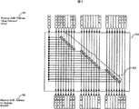
- FIG. 3 is a correlation diagram of addresses of the multilayer optical disc that is the first embodiment of the present invention.
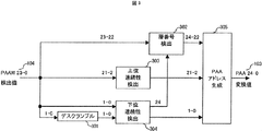
- FIG. 3 is a timing diagram of address detection in the first exemplary embodiment of the present invention.
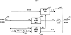
- FIG. 3 is a detection circuit diagram of address detection in the first exemplary embodiment of the present invention.
- FIG. 6 is a correlation diagram of addresses of a multilayer optical disc that is a second embodiment of the present invention.
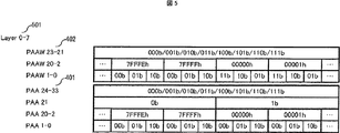
- FIG. 6 is a timing diagram of address detection in the second embodiment of the present invention.
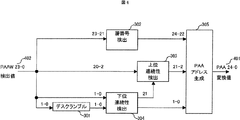
- FIG. 6 is a detection circuit diagram for address detection in a second exemplary embodiment of the present invention.
- FIG. 6 is a correlation diagram of addresses of a multilayer optical disc that is a third embodiment of the present invention.
- FIG. 6 is an example of a scramble circuit according to a third embodiment of the present invention.
- FIG. 10 is a timing diagram of address detection in a third embodiment of the present invention.
- FIG. 10 is a detection circuit diagram for address detection in a third exemplary embodiment of the present invention.
- FIG. 10 is a correlation diagram of addresses of an optical disc that is a fourth embodiment of the present invention.
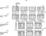
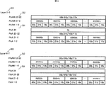
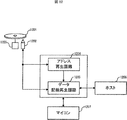
- 1 is an optical disc recording / reproducing apparatus according to a first embodiment of the present invention. It is an ADIP data structure figure of a multilayer optical disk. It is an ADIP word structure figure of a multilayer optical disk. It is an ADIP-Aux frame structure figure of a multilayer optical disk.
- FIG. 1 is a correlation diagram of addresses of a multilayer optical disk according to the first embodiment of the present invention.
- 101 is the physical sector number (hereinafter referred to as PSN) which is the physical sector number of the sector
- 102 is the address unit number (hereinafter referred to as AUN) which is the address embedded in the data of the cluster unit
- 103 is the physical ADIP address by wobble Is the actual address of the physical ADIP address (hereinafter referred to as PAA)
- PAAW the address actually embedded in the wobble of the physical ADIP address
- 105 is the scramble circuit
- 106 is the exclusive OR (Ex-OR) Show.
- scramble is one of arithmetic processes, and means a process for converting the value of each bit of an address or converting regularity.
- the upper 3 bits of PAA 103 are assigned to the layer number, and the conventional PAA An example of address extension from 24 bits to 1 bit is shown.
- the bit information of PAA bit 24, which is a virtual bit for address extension is assumed to be embedded in wobble in association with the lower 2 bits of PAA.
- a conventional PAA 24-bit configuration when assigned as a 3-bit layer number, 19-bit cluster number, and 2-bit intra-cluster count value, up to 8 layer numbers and 32 gigabytes per layer (64 kilobytes x 2 19 ) An address can be assigned to data having a data capacity of.
- the wobble address structure will be described.
- the ADIP address 24 bits (AA23-AA0) 104 recorded on the disc and the 12-bit auxiliary data (AUX data, AX11-AX0) 1301 for storing disc information are 36 bits.
- a structure having information bits is defined, and error correction code addition and code conversion are performed on the information bits to generate a code string per unit data.
- This code string is embedded in the wobble structure per unit period.
- a wobble structure with different wobble periodicity and phase is arranged based on certain rules, and a bit structure called ADIP unit is generated by expressing synchronization signals and data “0” and “1” due to the difference in arrangement etc. To do.
- the ADIP word structure diagram of Fig. 14 the data after the ADIP data 36 bit error correction code addition conversion to the 60 bits of data (4 ADIP bits ⁇ 15 blocks) in the structure of 1 ADIP word consisting of 83 bits A code string having a value of 60 bits is arranged.
- auxiliary data is composed of 96 words of 12-bit data structure and rearranged to form 144 bytes (12 bits x 96 words), and data indicating disk information and error correction codes are arranged. And has a sufficiently long update period with respect to the data cluster period.
- Either a 36-bit information bit structure, an error correction code addition method or conversion method for conversion into a code string, an arrangement period or wobble length, a correlation with a PSN, or a plurality of reviews is required.
- the structure becomes difficult to be compatible with the prior art, and the redundancy of the address generation / detection circuit and the complexity of the system control method become problems. Therefore, if the wobble address can be expanded without significantly modifying the wobble structure without changing the number of address bits embedded in the wobble, the control can be considerably facilitated.
- PAA 25 bits are allocated as the address range on the wobble.
- the number of bits of the address embedded in the disk using wobble is only 24 bits, so the most significant PAA bit 24 is transferred to other bits as a virtual address bit.
- the PAA bit 24 is input as a control bit for determining ON / OFF of the scramble process of the scramble circuit 105, and the lower two bits of the PAA bit 1-0 are subjected to scramble processing and embedded in the wobble.
- the PAA 1 bits 1-0 are the same as the conventional 0,1 , 2,0,1,2, ... and when PAA bit 24 is “1”, the value after exclusive OR operation is 3,2,1,3,2,1,... Will be counted. That is, the regularity of the count of the PAA bits 1-0 is changed according to the virtual bit PAA bits 24. Therefore, by actually embedding the PAAW bits 1-0, which are the output from the scramble circuit 105, in the wobble, it is possible to avoid embedding the virtual bits PAA bits 24 in the wobble. As an effect, it is possible to extend the address while maintaining the number of bits of the conventional wobble address.
- the descramble circuit 301 is scrambled by the exclusive OR 106 at the time of address generation, the result of the exclusive OR of “1” and the PAAW bits 1-0 is output after the descrambling operation.
- the virtual bit PAA bit 24 is assigned to the third bit of the layer number, the detection result differs depending on the layer number 0 to 3 (201) and the layer number 4 to 7 (202). Become.
- the PAAW bit 1-0 is input as 0,1,2,0,1,2, ... to the lower continuity detection circuit 304, so the PAA bit 24 is "0" “, PAA bits 1-0 will output PAAW bits 1-0 as they are.
- the PAAW bit 1-0 is input to the lower continuity detection circuit 304 as 3, 2, 1, 3, 2, 1,.
- the detection of the address detection value “3” and the decrement of continuity are detected to detect the presence of scramble processing at the time of address generation, and the PAA bit 24 is output as “1”.
- the lower PAA bits 1-0, 0, 1, 2, 0, 1, 2,... which are values after the descrambling process of the PAAW bits 1-0 are output.
- the in-cluster count value (PAA bits 1-0) is detected as the output of the lower continuity detection circuit 304, and further, the layer number detection circuit 302 from the generated PAA bit 24 and the PAAW bit 23-22 detected from the wobble.
- the generation of the layer number address (PAA bits 24-22) and the detection of the layer number are performed. Further, the higher address detection circuit 303 generates a cluster number address (PAA bit 21-2) and detects the cluster number from the PAAW bit 21-2 detected from the wobble. Therefore, the addresses obtained from the respective detection circuits 302, 303, and 304 are input to the PAA address generation circuit 305, and can be converted into addresses of PAA bits 24-0.
- the address structure of the wobble is not changed, and the physical address is not increased without increasing the number of bits of the address embedded in the wobble.
- the number of bits of the address indicating the target position can be expanded.
- the layer number address is expanded with virtual bits as the address assignment of the 2-bit layer number and the 20-bit cluster number, the layer number up to 8 layers and up to 64 GB Applicable to disk.
- it can be applied to disks with up to 16 layer numbers and 32 gigabytes per layer if used to expand the layer number address with the conventional 3-bit layer number and 19-bit cluster number address assignment.
- the virtual bits are controlled as scramble processing OFF in the case of layer numbers 0 to 3 as in this embodiment, the result is the same value as PAA bit 23-0 and PAAW bit 23-0. Compatibility with conventional optical discs can be maintained.
- FIG. 12 shows an example of a recording / reproducing apparatus that reproduces data from and records data from the optical disc created by the address generation described in this embodiment.
- Reference numeral 1201 denotes an optical disc
- 1202 denotes a pickup
- 1203 denotes a spindle motor
- 1204 denotes an address reproduction circuit
- 1205 denotes a data recording / reproduction circuit
- 1206 denotes an external host
- 1207 denotes a microcomputer that controls the entire system.
- a wobble signal read from the optical disk 1201 created using the address generation method shown in FIG. 1 via the pickup 1202 is input to the address reproduction circuit 1204 to detect address information.
- the address detection circuit described with reference to FIG. 3 it is possible to detect the position where data is recorded / reproduced, and to the host 1206 of the data obtained via the pickup 1202 and the data recording / reproduction circuit 1205. Data input / output and data recording / reproduction are possible.
- FIG. 4 is a correlation diagram of addresses of the multilayer optical disk according to the second embodiment of the present invention.
- the address is expanded using virtual bits that are not recorded on the disk while maintaining the ADIP data structure shown in FIG.
- the difference from FIG. 1 is that the virtual bit allocation is bit 21 instead of PAA bit 24.
- 401 is the actual address of Physical ADIP Address (hereinafter referred to as PAA)
- 402 is the wobble embedded address (hereinafter referred to as PAAW) of Physical ADIP Address, which is the same as in FIG.
- PAA Physical ADIP Address
- PAAW wobble embedded address
- the PAA bit 21 is input as a control bit for determining ON / OFF of the scramble process of the scramble circuit 105, and the lower 2 bits of the PAA bit 1-0 are scrambled. And embed in wobble. That is, the regularity of the count of the PAA bits 1-0 is changed according to the virtual bit PAA bits 21. As an effect, it is possible to extend the address while maintaining the number of bits of the conventional wobble address.
- the virtual bit PAA bit 21 is assigned not to the layer number address but to the cluster number address, so that address generation switching occurs in each layer.
- the low-order continuity detection circuit 304 detects the presence or absence of scramble processing as before. To generate a virtual bit PAA bit 21 and detect PAA 1-0.
- the count value in the cluster (PAA bits 1-0) is detected as an output of the lower continuity detection circuit 304, and the PAA bit 21 detected by the lower continuity detection circuit 304 and the PAAW bit 20- detected from the wobble. 2 is used to generate the cluster number address (PAA bits 21-2), detect the cluster number, and use the PAAW bits 23-22 detected from the wobble to generate the layer number address (PAA bits 24- 22) Detection is performed. Therefore, the addresses obtained from the respective detection circuits 302, 303, and 304 are input to the PAA address generation circuit 305, and can be converted into addresses of PAA bits 24-0.
- the address structure of the wobble is not changed, and the physical address is not increased without increasing the number of bits of the address embedded in the wobble.
- the number of bits of the address indicating the target position can be expanded.
- the virtual bit can be generated and detected in the same manner even if the virtual bit is assigned to the cluster number address of each layer instead of the layer number.
- the address detection circuit described in FIG. 6 is also used in the reproducing apparatus for reproducing data from the optical disk created by the address generation described in this embodiment and the recording apparatus for recording data on the optical disk. This makes it possible to detect the position where data is recorded and reproduced.
- FIG. 7 is a correlation diagram of addresses of the multilayer optical disk according to the third embodiment of the present invention.
- the address is expanded using virtual bits that are not recorded on the disk while maintaining the ADIP data structure shown in FIG.
- the difference from FIG. 1 is that the scrambling method is applied not only to the lower 2 bits of PAA bit 1-0 but also to the entire PAA 23-0.
- 701 is the actual address of Physical ADIP Address (hereinafter referred to as PAA)
- 702 is the wobble embedded address (hereinafter referred to as PAAW) of Physical ADIP ⁇ Address
- 703 is a scramble circuit similar to Fig. 1, but only the bit assignment is different, and the others are the same
- FIG. 1 is the actual address of Physical ADIP Address (hereinafter referred to as PAA)
- PAAW wobble embedded address
- 703 is a scramble circuit similar to Fig. 1, but only the bit assignment is different, and the others are the same
- FIG. 1 is the actual address of Physical ADIP Address
- FIG. 8 shows an example of a scramble circuit 703 which is a calculation process for embedding information.
- the exclusive OR 106 with the PAA bit 24 is used for each bit of the PAA bit 21-2 corresponding to the cluster number address, and other bits are input / output as they are. Therefore, when PAA bit 24 is “0”, PAA bit 21-2 increments to 0,1,2,3,4,5,..., FFFFFh, and PAA bit 24 is “1”.
- it since it is a value after the scramble processing, it is decremented to FFFFFh, FFFFEh, FFFFDh,.
- the regularity of the count of the PAA bit 21-2 is changed according to the virtual bit PAA bit 24. As an effect, it is possible to extend the address while maintaining the number of bits of the conventional wobble address.
- the PAA bit 24 which is a virtual bit, checks the continuity of the higher address of the PAAW 1-2 bit 21-2 and performs restoration. Also, as the scrambling method, since the upper 20 bits of PAA bits 21-2 are multiplied by exclusive OR 106, the presence or absence of scrambling in the upper continuity detection circuit 303 (in this example, the difference in continuity between increment and decrement) ) To generate a virtual bit PAA bit 24 and detect PAA 21-2.
- PAAW bit 21-2 is input as 0,1,2,3,4,5, ..., FFFFFh to upper continuity detection circuit 303, so PAA bit 24 is “0” and PAA bit 21-2 output PAAW bit 21-2 as it is.
- PAAW bit 21-2 is input as FFFFFh, FFFFEh, FFFFDh, ..., 0 to upper continuity detection circuit 303, so decrement is detected and PAA bit 24 is output as “1”, and is 0,1,2,3,4,5, ... which is the value after descrambling (in this example, exclusive OR of “1” and PAAW bit 21-2) , FFFFFh is output.
- the cluster number address (PAA (bits 21-2) can be generated and the cluster number can be detected as the output of the upper continuity detection circuit 303.
- the layer number detection circuit 302 generates the layer number address (PAA bits 24-22) and detects the layer number from the generated PAA bits 24 and the PAAW bits 23-22 detected from the wobble.
- the lower address detection circuit 304 detects the in-cluster count value (PAA bits 1-0) from the PAAW bits 1-0 detected from the wobble. Therefore, the addresses obtained from the respective detection circuits 302, 303, and 304 are input to the PAA address generation circuit 305, and can be converted into addresses of PAA bits 24-0.
- the address structure of the wobble is not changed, and the physical address is not increased without increasing the number of bits of the address embedded in the wobble.
- the number of bits of the address indicating the target position can be expanded.
- the virtual bit information can be generated and detected in the same manner by embedding not only a part of the address but also the entire address.
- the address detection circuit described in FIG. 10 is also used in the reproducing apparatus for reproducing data from the optical disk created by the address generation described in the present embodiment and the recording apparatus for recording data on the optical disk. This makes it possible to detect the position where data is recorded and reproduced.
- FIG. 11 is an address correlation diagram of an optical disc according to the fourth embodiment of the present invention.
- the address is expanded using virtual bits that are not recorded on the disc while maintaining the ADIP data structure shown in FIG.
- the difference from Fig. 7 is that 5 bits PAA bits 28-24 are used as virtual bits corresponding to PSN bits 31-27, PAA bit 28-2 is the cluster number, and PAA bits 1-0 are set as the structure of PAA 103. This is a point assigned as a count value in the cluster.
- 1101 is the actual address of Physical ADIP Address (hereinafter referred to as PAA)
- 1102 is the wobble embedded address of Physical ADIP Address (hereinafter referred to as PAAW)
- 1103 is the same as in FIG.
- the address structure of the wobble is not changed, and the physical address is not increased without increasing the number of bits of the address embedded in the wobble.
- the number of bits of the address indicating the target position can be expanded.
- the addresses composed of the layer number and the cluster number are explained using addresses composed only of the cluster number in the present embodiment. Is possible.
- the reproducing apparatus for reproducing data from the optical disk created by the address generation described in the present embodiment and the recording apparatus for recording data on the optical disk the position of the data recording / reproducing is similarly detected. Is possible.
- scramble is used as an information embedding method, and examples (105 in FIG. 1, 105 in FIG. 4, 703 in FIG. 7 and FIG. 8) are used as scramble circuits.
- the present invention is not limited, and any circuit or method that can embed information and detect information using bit operations based on the presence or absence of scramble or a difference in scramble regularity can be similarly applied.
- scramble means one of arithmetic processing, and any processing that converts each bit of an address or regularity It is not limited to scramble.
- the number of virtual bits, the position where the virtual bits are arranged, the bit position where information such as scramble information is embedded, and the bit configuration of the address are not limited to the present embodiment. However, it is better for the position where the virtual bit itself is arranged to change as an address considering the detection stability, and the bit position where information such as scramble information is embedded is changed as an address considering the detection time. More is better.
- the optical disk is used as a recording medium, and the address embedded in the wobble is used as the address.
- the present invention is not limited to this embodiment, and the address read from the generated address is not limited to this embodiment. If the idea of reducing bits so as to reduce the number of bits can be applied, the application can be similarly performed.
- the virtual bit is not embedded in the wobble, it may be stored in an area different from the read address area and used for address detection.
- PAW Physical ADIP Address
- 1103 Scramble circuit, 1201 ... Optical disk, 1202 ... Pickup, 1203 ... Spindle motor, 1204 ... Address reproduction circuit, 1205 ... Data recording / reproduction circuit, 1206 ... Host, 1207 ... Microcomputer, 1301 ... AUX data.
Landscapes
- Engineering & Computer Science (AREA)
- Multimedia (AREA)
- Signal Processing (AREA)
- Optical Recording Or Reproduction (AREA)
- Signal Processing For Digital Recording And Reproducing (AREA)
Abstract
Description
24ビットから1bitのアドレス拡張した場合の例を示す。また、アドレス拡張の仮想ビットであるPAA ビット24のビット情報は、PAAの下位2ビットに関連付けてウォブルに埋め込むものとする。従来のPAA 24ビット構成において、3ビットの層番号、19ビットのクラスタ番号、2ビットのクラスタ内カウント値として割り付けた場合、8層までの層番号と各層あたり32ギガバイト(64キロバイト×219)のデータ容量のデータに対してアドレスを割り当てることが出来る。しかし、各層あたり32ギガバイトを越える高密度な光ディスクの場合に、クラスタ番号を20ビットに拡張することで各層あたり64ギガバイト(64キロバイト×220)のデータ容量のデータに対してアドレスを割り付けることが出来るが、層番号のビットが2ビットに減ってしまうため5層以上のアドレス生成ができなくなってしまう。そこで、層番号として1ビット拡張し、従来と同等の3ビットにより8層までのアドレスを生成する。
Claims (6)
- 複数のデータを記録するクラスタを有する記録媒体において、
前記クラスタに同期してデータを記録するトラックにウォブリング重畳されて記録されているアドレスを有し、
前記アドレスは記録媒体の物理的な位置を示すアドレス情報であり、ディスク情報を含む補助情報とでデータ構造を構成し、誤り訂正符号を付加してコード列を生成し、前記コード列を変調して記録されており、
複数の前記データ構造に含まれる補助情報は集められて、ブロックをなし、誤り訂正符号が付加され、
前記アドレス情報は、該アドレスの全体もしくは一部の変換の有無や規則性の切り替え有無を示す仮想ビットを有し、
前記仮想ビットを用いて変換もしくは規則性の切り替えられた後のアドレス情報が記録されていることを特徴とする記録媒体。 - 複数のデータを記録するクラスタを有する記録媒体における記録方法であって、
前記クラスタに同期してデータを記録するトラックにウォブリング重畳されて記録されているアドレスを有し、
前記アドレスは記録媒体の物理的な位置を示すアドレス情報であり、ディスク情報を含む補助情報とでデータ構造を構成し、誤り訂正符号を付加してコード列を生成し、前記コード列を変調して記録されており、
複数の前記データ構造に含まれる補助情報は集められて、ブロックをなし、誤り訂正符号が付加され、
前記アドレス情報は、該アドレスの全体もしくは一部の変換の有無や規則性の切り替え有無を示す仮想ビットを有し、
前記仮想ビットを用いて変換された後のアドレス情報が記録してある記録媒体にデータを記録する記録方法であって、
記録時の規則に従って前記アドレスによりデータ位置を検出して記録することを特徴とする記録方法。 - 複数のデータを記録するクラスタを有する記録媒体における再生方法であって、
前記クラスタに同期してデータを記録するトラックにウォブリング重畳されて記録されているアドレスを有し、
前記アドレスは記録媒体の物理的な位置を示すアドレス情報であり、ディスク情報を含む補助情報とでデータ構造を構成し、誤り訂正符号を付加してコード列を生成し、前記コード列を変調して記録されており、
複数の前記データ構造に含まれる補助情報は集められて、ブロックをなし、誤り訂正符号が付加され、
前記アドレス情報は、該アドレスの全体もしくは一部の変換の有無や規則性の切り替え有無を示す仮想ビットを有し、
前記仮想ビットを用いて変換された後のアドレス情報が記録してある記録媒体からデータを再生する再生方法であって、
記録時の規則に従って前記アドレス情報によりデータ位置を検出して再生することを特徴とする再生方法。 - 複数のデータを記録するクラスタを有する記録媒体にデータを記録する記録方法であって、
前記クラスタに同期した、記録媒体の物理的な位置を示すアドレス情報は、前記アドレスの全体もしくは一部の変換の有無や規則性の切り替え有無を示す仮想ビットを有し、
前記仮想ビットを用いて変換もしくは規則性の変換処理後のアドレス情報を、ディスク情報を含み、ブロックをなし、誤り訂正符号が吹かされた補助情報をn分割(n:整数)したデータとでデータ構造を構成し、誤り訂正符号を付加してコード列を生成し、前記コード列を変調し、データを記録するトラックにウォブリング重畳し、記録媒体へ記録することを特徴とする記録方法。 - 複数のデータを記録するクラスタを有する記録媒体からデータを再生する再生装置において、
前記クラスタに同期してデータを記録するトラックにウォブリング重畳されて記録されているアドレスを有し、
前記アドレスは記録媒体の物理的な位置を示すアドレス情報であり、ディスク情報を含む補助情報とでデータ構造を構成し、誤り訂正符号を付加してコード列を生成し、前記コード列を変調して記録されており、
複数の前記データ構造に含まれる補助情報は集められて、ブロックをなし、誤り訂正符号が付加され、
前記アドレス情報は、該アドレスの全体もしくは一部の変換の有無や規則性の切り替え有無を示す仮想ビットを有し、
前記仮想ビットを用いて変換もしくは規則性が切り替えされた後のアドレス情報が記録してある記録媒体からデータを読み込む手段と、
ウォブルより検出されたアドレス情報から、アドレス全体もしくは一部のビット変換の有無や規則性の切り替え有無から仮想ビットを検出する手段と、
前記仮想ビットの検出結果より前記アドレスを検出する手段と、
検出した前記アドレスからデータ位置を検出する手段を具備することを特徴とする再生装置。 - 複数のデータを記録するエリアと前記データに体操して物理的な記録位置を示すアドレスを有する記録媒体において、
前記アドレスへのスクランブル有無や規則性を切り替えるための仮想ビットを前記アドレスの拡張ビットとして用い、
前記スクランブル後のアドレスが記録されていることを特徴とする記録媒体。
Priority Applications (2)
| Application Number | Priority Date | Filing Date | Title |
|---|---|---|---|
| US13/577,379 US8593919B2 (en) | 2010-03-05 | 2010-11-10 | Recording medium, reproduction and recording method, reproduction and recording device |
| CN2010800632302A CN102792375B (zh) | 2010-03-05 | 2010-11-10 | 记录介质、再现和记录方法、再现和记录装置 |
Applications Claiming Priority (2)
| Application Number | Priority Date | Filing Date | Title |
|---|---|---|---|
| JP2010-048578 | 2010-03-05 | ||
| JP2010048578A JP5119284B2 (ja) | 2010-03-05 | 2010-03-05 | 記録媒体、再生及び記録方法、再生及び記録装置 |
Publications (1)
| Publication Number | Publication Date |
|---|---|
| WO2011108148A1 true WO2011108148A1 (ja) | 2011-09-09 |
Family
ID=44541824
Family Applications (1)
| Application Number | Title | Priority Date | Filing Date |
|---|---|---|---|
| PCT/JP2010/070010 Ceased WO2011108148A1 (ja) | 2010-03-05 | 2010-11-10 | 記録媒体、再生及び記録方法、再生及び記録装置 |
Country Status (4)
| Country | Link |
|---|---|
| US (1) | US8593919B2 (ja) |
| JP (1) | JP5119284B2 (ja) |
| CN (1) | CN102792375B (ja) |
| WO (1) | WO2011108148A1 (ja) |
Families Citing this family (5)
| Publication number | Priority date | Publication date | Assignee | Title |
|---|---|---|---|---|
| JP5070231B2 (ja) * | 2009-02-12 | 2012-11-07 | 株式会社日立製作所 | 記録媒体、アドレス生成及び検出方法、再生及び記録装置 |
| JP5011326B2 (ja) * | 2009-02-24 | 2012-08-29 | 株式会社日立製作所 | 情報記録媒体、アドレス生成及び検出方法、再生及び記録装置 |
| JP5119286B2 (ja) | 2010-03-05 | 2013-01-16 | 日立コンシューマエレクトロニクス株式会社 | 記録媒体、再生及び記録方法、再生及び記録装置 |
| JP5119283B2 (ja) | 2010-03-05 | 2013-01-16 | 日立コンシューマエレクトロニクス株式会社 | 記録媒体、再生及び記録方法、再生及び記録装置 |
| JP5119285B2 (ja) | 2010-03-05 | 2013-01-16 | 日立コンシューマエレクトロニクス株式会社 | 記録媒体、再生及び記録方法、再生及び記録装置 |
Citations (7)
| Publication number | Priority date | Publication date | Assignee | Title |
|---|---|---|---|---|
| JP2002319246A (ja) * | 2001-04-20 | 2002-10-31 | Sony Corp | 記録媒体、及びその製造装置、製造方法、記録再生装置並びに再生方法 |
| JP2003123333A (ja) * | 2001-10-09 | 2003-04-25 | Sony Corp | ディスク記録媒体、ディスクドライブ装置、再生方法、ディスク製造方法 |
| JP2006269077A (ja) * | 2006-06-05 | 2006-10-05 | Hitachi Ltd | 光情報記録媒体 |
| WO2008060104A1 (en) * | 2006-11-17 | 2008-05-22 | Samsung Electronics Co, . Ltd. | Optical recording medium, apparatus and method of manufacturing optical recording medium, and apparatus and method of recording/reproducing data of optical recording medium |
| JP2008523534A (ja) * | 2004-12-08 | 2008-07-03 | コーニンクレッカ フィリップス エレクトロニクス エヌ ヴィ | 記録担体のアドレス空間を拡張する装置及び方法 |
| JP2010186507A (ja) * | 2009-02-12 | 2010-08-26 | Hitachi Ltd | 記録媒体、アドレス生成及び検出方法、再生及び記録装置 |
| JP2010198665A (ja) * | 2009-02-24 | 2010-09-09 | Hitachi Ltd | 情報記録媒体、アドレス生成及び検出方法、再生及び記録装置 |
Family Cites Families (8)
| Publication number | Priority date | Publication date | Assignee | Title |
|---|---|---|---|---|
| KR100750624B1 (ko) * | 1999-09-29 | 2007-08-20 | 소니 가부시끼 가이샤 | 데이터 기록매체, 데이터 기록 및/또는 재생장치 및기록매체 판별방법 |
| JP2001243722A (ja) * | 2000-02-29 | 2001-09-07 | Sony Corp | ディスク記録媒体、及びディスクドライブ装置 |
| TWI359409B (en) | 2002-06-05 | 2012-03-01 | Lg Electronics Inc | High-density optical disc, method for recording an |
| JP4544435B2 (ja) | 2009-02-10 | 2010-09-15 | 日本電気株式会社 | 映像品質推定装置、映像品質推定方法およびプログラム |
| JP5018804B2 (ja) | 2009-02-24 | 2012-09-05 | 株式会社日立製作所 | アドレス生成及び検出方法、再生及び記録装置 |
| JP5119283B2 (ja) | 2010-03-05 | 2013-01-16 | 日立コンシューマエレクトロニクス株式会社 | 記録媒体、再生及び記録方法、再生及び記録装置 |
| JP5119285B2 (ja) | 2010-03-05 | 2013-01-16 | 日立コンシューマエレクトロニクス株式会社 | 記録媒体、再生及び記録方法、再生及び記録装置 |
| JP5119286B2 (ja) | 2010-03-05 | 2013-01-16 | 日立コンシューマエレクトロニクス株式会社 | 記録媒体、再生及び記録方法、再生及び記録装置 |
-
2010
- 2010-03-05 JP JP2010048578A patent/JP5119284B2/ja active Active
- 2010-11-10 CN CN2010800632302A patent/CN102792375B/zh not_active Expired - Fee Related
- 2010-11-10 WO PCT/JP2010/070010 patent/WO2011108148A1/ja not_active Ceased
- 2010-11-10 US US13/577,379 patent/US8593919B2/en not_active Expired - Fee Related
Patent Citations (7)
| Publication number | Priority date | Publication date | Assignee | Title |
|---|---|---|---|---|
| JP2002319246A (ja) * | 2001-04-20 | 2002-10-31 | Sony Corp | 記録媒体、及びその製造装置、製造方法、記録再生装置並びに再生方法 |
| JP2003123333A (ja) * | 2001-10-09 | 2003-04-25 | Sony Corp | ディスク記録媒体、ディスクドライブ装置、再生方法、ディスク製造方法 |
| JP2008523534A (ja) * | 2004-12-08 | 2008-07-03 | コーニンクレッカ フィリップス エレクトロニクス エヌ ヴィ | 記録担体のアドレス空間を拡張する装置及び方法 |
| JP2006269077A (ja) * | 2006-06-05 | 2006-10-05 | Hitachi Ltd | 光情報記録媒体 |
| WO2008060104A1 (en) * | 2006-11-17 | 2008-05-22 | Samsung Electronics Co, . Ltd. | Optical recording medium, apparatus and method of manufacturing optical recording medium, and apparatus and method of recording/reproducing data of optical recording medium |
| JP2010186507A (ja) * | 2009-02-12 | 2010-08-26 | Hitachi Ltd | 記録媒体、アドレス生成及び検出方法、再生及び記録装置 |
| JP2010198665A (ja) * | 2009-02-24 | 2010-09-09 | Hitachi Ltd | 情報記録媒体、アドレス生成及び検出方法、再生及び記録装置 |
Also Published As
| Publication number | Publication date |
|---|---|
| JP5119284B2 (ja) | 2013-01-16 |
| US20120300609A1 (en) | 2012-11-29 |
| CN102792375A (zh) | 2012-11-21 |
| JP2011187096A (ja) | 2011-09-22 |
| CN102792375B (zh) | 2013-11-06 |
| US8593919B2 (en) | 2013-11-26 |
Similar Documents
| Publication | Publication Date | Title |
|---|---|---|
| JP5070231B2 (ja) | 記録媒体、アドレス生成及び検出方法、再生及び記録装置 | |
| US8289820B2 (en) | Address generating and detecting method and reproducing and recording apparatus | |
| JP5119283B2 (ja) | 記録媒体、再生及び記録方法、再生及び記録装置 | |
| JP5119284B2 (ja) | 記録媒体、再生及び記録方法、再生及び記録装置 | |
| JP5119285B2 (ja) | 記録媒体、再生及び記録方法、再生及び記録装置 | |
| JP5119286B2 (ja) | 記録媒体、再生及び記録方法、再生及び記録装置 | |
| JP5011326B2 (ja) | 情報記録媒体、アドレス生成及び検出方法、再生及び記録装置 | |
| JP5544389B2 (ja) | アドレス生成及び検出方法、再生及び記録装置 | |
| JP2013051022A (ja) | 記録媒体、再生及び記録方法、再生及び記録装置 | |
| JP2012256420A (ja) | 記録媒体、アドレス生成及び検出方法、再生及び記録装置 |
Legal Events
| Date | Code | Title | Description |
|---|---|---|---|
| WWE | Wipo information: entry into national phase |
Ref document number: 201080063230.2 Country of ref document: CN |
|
| 121 | Ep: the epo has been informed by wipo that ep was designated in this application |
Ref document number: 10847045 Country of ref document: EP Kind code of ref document: A1 |
|
| WWE | Wipo information: entry into national phase |
Ref document number: 13577379 Country of ref document: US |
|
| NENP | Non-entry into the national phase |
Ref country code: DE |
|
| 122 | Ep: pct application non-entry in european phase |
Ref document number: 10847045 Country of ref document: EP Kind code of ref document: A1 |