WO2011104965A1 - 立体映像表示装置、立体映像表示システム、および立体映像表示装置の駆動方法 - Google Patents
立体映像表示装置、立体映像表示システム、および立体映像表示装置の駆動方法 Download PDFInfo
- Publication number
- WO2011104965A1 WO2011104965A1 PCT/JP2010/071382 JP2010071382W WO2011104965A1 WO 2011104965 A1 WO2011104965 A1 WO 2011104965A1 JP 2010071382 W JP2010071382 W JP 2010071382W WO 2011104965 A1 WO2011104965 A1 WO 2011104965A1
- Authority
- WO
- WIPO (PCT)
- Prior art keywords
- liquid crystal
- storage capacitor
- video
- data
- display device
- Prior art date
- Legal status (The legal status is an assumption and is not a legal conclusion. Google has not performed a legal analysis and makes no representation as to the accuracy of the status listed.)
- Ceased
Links
Images







Classifications
-
- G—PHYSICS
- G02—OPTICS
- G02B—OPTICAL ELEMENTS, SYSTEMS OR APPARATUS
- G02B30/00—Optical systems or apparatus for producing three-dimensional [3D] effects, e.g. stereoscopic images
- G02B30/20—Optical systems or apparatus for producing three-dimensional [3D] effects, e.g. stereoscopic images by providing first and second parallax images to an observer's left and right eyes
- G02B30/22—Optical systems or apparatus for producing three-dimensional [3D] effects, e.g. stereoscopic images by providing first and second parallax images to an observer's left and right eyes of the stereoscopic type
- G02B30/24—Optical systems or apparatus for producing three-dimensional [3D] effects, e.g. stereoscopic images by providing first and second parallax images to an observer's left and right eyes of the stereoscopic type involving temporal multiplexing, e.g. using sequentially activated left and right shutters
-
- G—PHYSICS
- G09—EDUCATION; CRYPTOGRAPHY; DISPLAY; ADVERTISING; SEALS
- G09G—ARRANGEMENTS OR CIRCUITS FOR CONTROL OF INDICATING DEVICES USING STATIC MEANS TO PRESENT VARIABLE INFORMATION
- G09G3/00—Control arrangements or circuits, of interest only in connection with visual indicators other than cathode-ray tubes
- G09G3/001—Control arrangements or circuits, of interest only in connection with visual indicators other than cathode-ray tubes using specific devices not provided for in groups G09G3/02 - G09G3/36, e.g. using an intermediate record carrier such as a film slide; Projection systems; Display of non-alphanumerical information, solely or in combination with alphanumerical information, e.g. digital display on projected diapositive as background
- G09G3/003—Control arrangements or circuits, of interest only in connection with visual indicators other than cathode-ray tubes using specific devices not provided for in groups G09G3/02 - G09G3/36, e.g. using an intermediate record carrier such as a film slide; Projection systems; Display of non-alphanumerical information, solely or in combination with alphanumerical information, e.g. digital display on projected diapositive as background to produce spatial visual effects
-
- G—PHYSICS
- G09—EDUCATION; CRYPTOGRAPHY; DISPLAY; ADVERTISING; SEALS
- G09G—ARRANGEMENTS OR CIRCUITS FOR CONTROL OF INDICATING DEVICES USING STATIC MEANS TO PRESENT VARIABLE INFORMATION
- G09G3/00—Control arrangements or circuits, of interest only in connection with visual indicators other than cathode-ray tubes
- G09G3/20—Control arrangements or circuits, of interest only in connection with visual indicators other than cathode-ray tubes for presentation of an assembly of a number of characters, e.g. a page, by composing the assembly by combination of individual elements arranged in a matrix no fixed position being assigned to or needed to be assigned to the individual characters or partial characters
- G09G3/22—Control arrangements or circuits, of interest only in connection with visual indicators other than cathode-ray tubes for presentation of an assembly of a number of characters, e.g. a page, by composing the assembly by combination of individual elements arranged in a matrix no fixed position being assigned to or needed to be assigned to the individual characters or partial characters using controlled light sources
- G09G3/30—Control arrangements or circuits, of interest only in connection with visual indicators other than cathode-ray tubes for presentation of an assembly of a number of characters, e.g. a page, by composing the assembly by combination of individual elements arranged in a matrix no fixed position being assigned to or needed to be assigned to the individual characters or partial characters using controlled light sources using electroluminescent panels
- G09G3/32—Control arrangements or circuits, of interest only in connection with visual indicators other than cathode-ray tubes for presentation of an assembly of a number of characters, e.g. a page, by composing the assembly by combination of individual elements arranged in a matrix no fixed position being assigned to or needed to be assigned to the individual characters or partial characters using controlled light sources using electroluminescent panels semiconductive, e.g. using light-emitting diodes [LED]
- G09G3/3208—Control arrangements or circuits, of interest only in connection with visual indicators other than cathode-ray tubes for presentation of an assembly of a number of characters, e.g. a page, by composing the assembly by combination of individual elements arranged in a matrix no fixed position being assigned to or needed to be assigned to the individual characters or partial characters using controlled light sources using electroluminescent panels semiconductive, e.g. using light-emitting diodes [LED] organic, e.g. using organic light-emitting diodes [OLED]
- G09G3/3225—Control arrangements or circuits, of interest only in connection with visual indicators other than cathode-ray tubes for presentation of an assembly of a number of characters, e.g. a page, by composing the assembly by combination of individual elements arranged in a matrix no fixed position being assigned to or needed to be assigned to the individual characters or partial characters using controlled light sources using electroluminescent panels semiconductive, e.g. using light-emitting diodes [LED] organic, e.g. using organic light-emitting diodes [OLED] using an active matrix
- G09G3/3233—Control arrangements or circuits, of interest only in connection with visual indicators other than cathode-ray tubes for presentation of an assembly of a number of characters, e.g. a page, by composing the assembly by combination of individual elements arranged in a matrix no fixed position being assigned to or needed to be assigned to the individual characters or partial characters using controlled light sources using electroluminescent panels semiconductive, e.g. using light-emitting diodes [LED] organic, e.g. using organic light-emitting diodes [OLED] using an active matrix with pixel circuitry controlling the current through the light-emitting element
-
- G—PHYSICS
- G09—EDUCATION; CRYPTOGRAPHY; DISPLAY; ADVERTISING; SEALS
- G09G—ARRANGEMENTS OR CIRCUITS FOR CONTROL OF INDICATING DEVICES USING STATIC MEANS TO PRESENT VARIABLE INFORMATION
- G09G3/00—Control arrangements or circuits, of interest only in connection with visual indicators other than cathode-ray tubes
- G09G3/20—Control arrangements or circuits, of interest only in connection with visual indicators other than cathode-ray tubes for presentation of an assembly of a number of characters, e.g. a page, by composing the assembly by combination of individual elements arranged in a matrix no fixed position being assigned to or needed to be assigned to the individual characters or partial characters
- G09G3/34—Control arrangements or circuits, of interest only in connection with visual indicators other than cathode-ray tubes for presentation of an assembly of a number of characters, e.g. a page, by composing the assembly by combination of individual elements arranged in a matrix no fixed position being assigned to or needed to be assigned to the individual characters or partial characters by control of light from an independent source
- G09G3/36—Control arrangements or circuits, of interest only in connection with visual indicators other than cathode-ray tubes for presentation of an assembly of a number of characters, e.g. a page, by composing the assembly by combination of individual elements arranged in a matrix no fixed position being assigned to or needed to be assigned to the individual characters or partial characters by control of light from an independent source using liquid crystals
- G09G3/3611—Control of matrices with row and column drivers
- G09G3/3648—Control of matrices with row and column drivers using an active matrix
- G09G3/3659—Control of matrices with row and column drivers using an active matrix the addressing of the pixel involving the control of two or more scan electrodes or two or more data electrodes, e.g. pixel voltage dependant on signal of two data electrodes
-
- H—ELECTRICITY
- H04—ELECTRIC COMMUNICATION TECHNIQUE
- H04N—PICTORIAL COMMUNICATION, e.g. TELEVISION
- H04N13/00—Stereoscopic video systems; Multi-view video systems; Details thereof
- H04N13/30—Image reproducers
- H04N13/332—Displays for viewing with the aid of special glasses or head-mounted displays [HMD]
- H04N13/341—Displays for viewing with the aid of special glasses or head-mounted displays [HMD] using temporal multiplexing
-
- H—ELECTRICITY
- H04—ELECTRIC COMMUNICATION TECHNIQUE
- H04N—PICTORIAL COMMUNICATION, e.g. TELEVISION
- H04N13/00—Stereoscopic video systems; Multi-view video systems; Details thereof
- H04N13/30—Image reproducers
- H04N13/398—Synchronisation thereof; Control thereof
-
- G—PHYSICS
- G09—EDUCATION; CRYPTOGRAPHY; DISPLAY; ADVERTISING; SEALS
- G09G—ARRANGEMENTS OR CIRCUITS FOR CONTROL OF INDICATING DEVICES USING STATIC MEANS TO PRESENT VARIABLE INFORMATION
- G09G2300/00—Aspects of the constitution of display devices
- G09G2300/08—Active matrix structure, i.e. with use of active elements, inclusive of non-linear two terminal elements, in the pixels together with light emitting or modulating elements
- G09G2300/0809—Several active elements per pixel in active matrix panels
- G09G2300/0842—Several active elements per pixel in active matrix panels forming a memory circuit, e.g. a dynamic memory with one capacitor
-
- G—PHYSICS
- G09—EDUCATION; CRYPTOGRAPHY; DISPLAY; ADVERTISING; SEALS
- G09G—ARRANGEMENTS OR CIRCUITS FOR CONTROL OF INDICATING DEVICES USING STATIC MEANS TO PRESENT VARIABLE INFORMATION
- G09G2310/00—Command of the display device
- G09G2310/02—Addressing, scanning or driving the display screen or processing steps related thereto
- G09G2310/0243—Details of the generation of driving signals
- G09G2310/0251—Precharge or discharge of pixel before applying new pixel voltage
-
- G—PHYSICS
- G09—EDUCATION; CRYPTOGRAPHY; DISPLAY; ADVERTISING; SEALS
- G09G—ARRANGEMENTS OR CIRCUITS FOR CONTROL OF INDICATING DEVICES USING STATIC MEANS TO PRESENT VARIABLE INFORMATION
- G09G2310/00—Command of the display device
- G09G2310/02—Addressing, scanning or driving the display screen or processing steps related thereto
- G09G2310/0262—The addressing of the pixel, in a display other than an active matrix LCD, involving the control of two or more scan electrodes or two or more data electrodes, e.g. pixel voltage dependent on signals of two data electrodes
Definitions
- the present invention relates to a stereoscopic video display device that displays a stereoscopic video by alternately displaying a left-eye video and a right-eye video for each frame period in a time-sharing manner, and a stereoscopic video display system having the stereoscopic video display device. It is about.
- LCDs consume less power than CRT (Cathode Ray Ray Tube) displays and are easy to miniaturize, so they are widely used in TVs, mobile phones, portable game consoles, and in-vehicle navigation systems. .
- CRT Cathode Ray Ray Tube
- a left-eye image and a right-eye image are alternately displayed for each frame period in a time-sharing manner, and a user closes and opens a left-eye shutter and a right-eye shutter.
- a technique for displaying a stereoscopic image to a user by wearing shutter glasses having an eye shutter has been proposed.
- Patent Document 1 only the left-eye video in the vertical blanking period of the liquid crystal display among the frame periods of the left-eye video and the right-eye video displayed on the liquid crystal display is displayed on the left eye.
- a method has been proposed in which shutter glasses are opened and closed so that only the right-eye video in the vertical blanking period is displayed on the right eye. This eliminates the problem of so-called crosstalk, in which a video in which left-eye video and right-eye video are mixed is displayed to the user. This point will be described below.
- FIG. 11 shows a timing chart when the opening and closing of the shutter glasses is controlled by the method described in Patent Document 1.
- reference numeral 206 schematically shows video data output to a liquid crystal display that alternately displays a left-eye video (Leftn) and a right-eye video (Rightn) for each frame period by time division. It is.
- the liquid crystal display also includes shutter glasses having a liquid crystal shutter L (left eye shutter) for closing and opening the left eye and a liquid crystal shutter R (right eye shutter) for closing and opening the right eye, and a shutter. And a liquid crystal shutter controller for controlling the closing and opening of the liquid crystal shutters L and R of the glasses.
- FIG. 11 shows a timing chart of a liquid crystal shutter L control signal 208 for controlling opening / closing of the liquid crystal shutter L and a timing chart of a liquid crystal shutter R control signal 209 for controlling opening / closing of the liquid crystal shutter R.
- overlap periods 501, 502, and 503 which are periods during which pixel data is actually sent out, in accordance with the vertical synchronization signal, and the start of the next frame period
- a vertical blanking period 504 that is a period during which transmission of pixel data is suspended.
- the video of a certain frame period for example, the left-eye video Left1
- the video of the next frame period for example, the right-eye video Right1
- the vertical blanking period 504 only the left-eye video and the right-eye video in which the images are not mixed are displayed.
- the liquid crystal shutter control unit performs vertical buzzing of the liquid crystal display in each frame period of the left eye video and the right eye video displayed on the liquid crystal display. Only in the ranking period 504, control is performed such that the left and right eyes are opened in the liquid crystal shutters L and R of the shutter glasses.
- the liquid crystal shutter is opened only for about a quarter of the entire frame period for each of the left-eye video and the right-eye video. Further, in the case of a full high-definition TV signal, the opening time is further shortened due to transmission speed limitations and the like, and the liquid crystal shutter is opened only at about 15% of the total frame period, and practically only about 4%. As a result, the entire screen becomes dark, resulting in a problem that it is difficult to view the displayed stereoscopic video.
- the first left-eye frame L1 and the first left-eye frame L1 are displayed in the left-eye video display period.
- the second left-eye frame L2 is sequentially displayed, and the first right-eye frame R1 and the second right-eye frame R2 of the same image as the first right-eye frame R1 are sequentially displayed during the right-eye video display period. is doing.
- the same video frame is displayed twice in succession, so that the time for which the right-eye video and the left-eye video frame are determined is determined. Since it can be extended, it is described that the displayed stereoscopic image can be easily viewed.
- the opening period of the liquid crystal shutter is longer than that of Patent Document 1, in principle it can be opened only about 1/2 of the entire frame period.
- the present invention has been made in view of the above problems, and provides a shutter glasses-type stereoscopic video display device and a stereoscopic video display system capable of displaying a bright stereoscopic video without increasing the frame frequency. With the goal.
- a stereoscopic video display device is a stereoscopic video display device that displays a left-eye video and a right-eye video for performing stereoscopic video display in a time-sharing manner.
- the stereoscopic image display apparatus includes a display panel, and the display panel includes a plurality of data signal lines, a plurality of scanning signal lines intersecting with the plurality of data signal lines, the plurality of data signal lines, and the A pixel unit arranged in a matrix corresponding to each intersection with a plurality of scanning signal lines, and the pixel unit includes a first switching element connected to the scanning signal line and the data signal line A first storage capacitor portion that contributes to display by holding the data potential supplied from the data signal line, and a first storage capacitor portion that holds the data potential before applying it to the first storage capacitor. 2 holding capacity , And a second switching element disposed between the first storage capacitor unit and the second storage capacitor unit, wherein the first switching element scans from the scanning signal line.
- the second switching element is turned on by a signal and applies the data potential supplied from the data signal line to the second storage capacitor portion, and the second switching element is in a period during which the scanning signal line is scanning.
- the display device is characterized in that the video potential displayed on the pixel portion is switched by applying a data potential to the first storage capacitor portion by switching to the on state in the off state.
- the stereoscopic video display device of the present invention is a display device that realizes stereoscopic video display using a shutter glasses method.
- switching is performed with a first storage capacitor portion (corresponding to a liquid crystal capacitor in the case of a liquid crystal display device) provided in a normal liquid crystal display panel in each pixel portion arranged in a matrix.
- the second holding capacitor for temporarily holding the data potential and the first time when the scanning signal line is not scanned (the blanking period) are turned on.
- a switching element (second switching element) that applies a data potential to the storage capacitor portion and switches an image displayed on the pixel portion.
- the second storage capacitor unit that temporarily holds the data potential before being applied to the first storage capacitor unit is provided, so that the current image is displayed in the first storage capacitor unit. While the data potential of the data (current frame) is held and the display based on the data potential is being performed, the next video data (in the second holding capacitor portion of each pixel is scanned by scanning the scanning signal line. The data potential of the next frame) can be charged sequentially.
- the second switching element provided in each pixel is collectively switched from the off state to the on state using a period in which the scanning signal line is not scanned, so that the second switching element of each pixel portion in the display panel is switched.
- a data potential based on the next video data charged in the second storage capacitor unit can be collectively applied to one storage capacitor unit.
- the first storage capacitor that contributes to the display of each pixel can be charged collectively in units of one piece of video data (one frame), a frame period peculiar to a display panel that performs line sequential scanning. “Delay” of each video is less likely to occur. Therefore, when the display device having the above-described configuration is observed with shutter glasses, the right eye image and the left eye image are mixed even if each of the left eye shutter and the right eye shutter of the shutter glasses is opened for a relatively long time. Can be prevented. Therefore, overlapping of pictures can be suppressed without increasing the frame frequency, and a bright stereoscopic image can be displayed.
- a stereoscopic video display system corresponds to the stereoscopic video display device, and a left-eye video and a right-eye video corresponding to each of a left-eye video and a right-eye video. And a shutter part for selectively transmitting each video.
- the stereoscopic video display system of the present invention realizes stereoscopic video display using the shutter glasses method. Since the stereoscopic video display system of the present invention includes the stereoscopic video display device of the present invention, a bright stereoscopic video can be displayed without increasing the frame frequency. Accordingly, an observer who visually recognizes an image using the shutter unit can see a stereoscopic image that is bright and does not overlap the left and right images.
- a driving method of a stereoscopic video display device is a driving method of a stereoscopic video display device according to the present invention, wherein a current out of a plurality of video data displayed in the time-division manner on the first holding capacitor. While the data potential based on the video data is held, the first switching element is turned on while the second switching element is turned off, and the time is displayed on the second holding capacitor in the time division manner. And charging the data potential based on the next video data of the plurality of video data to be turned on, and turning on the second switching element in each pixel in a state where the first switching element is turned off. As a result, the data potential based on the next video data charged in the second storage capacitor is collectively applied to the first storage capacitor of each pixel, and display based on the data potential is performed. Characterized in that it comprises a and.
- the second storage capacitor unit that temporarily holds the data potential before being applied to the first storage capacitor unit is provided, so that the current image is displayed in the first storage capacitor unit. While the data potential of the data (current frame) is held and the display based on the data potential is being performed, the next video data (in the second holding capacitor portion of each pixel is scanned by scanning the scanning signal line. The data potential of the next frame) can be charged sequentially.
- the second switching element provided in each pixel is collectively switched from the off state to the on state using a period in which the scanning signal line is not scanned, so that the second switching element of each pixel portion in the display panel is switched.
- a data potential based on the next video data charged in the second storage capacitor unit can be collectively applied to one storage capacitor unit.
- the first storage capacitor that contributes to the display of each pixel can be charged collectively in units of one piece of video data (one frame), a frame period peculiar to a display panel that performs line sequential scanning. “Delay” of each video is less likely to occur. Therefore, when observing the image displayed by the above method with the shutter glasses, the right-eye image and the left-eye image can be obtained even if each of the left eye shutter and the right eye shutter of the shutter glasses has a relatively long open time. Can be prevented. Therefore, overlapping of pictures can be suppressed without increasing the frame frequency, and a bright stereoscopic image can be displayed.
- the stereoscopic video display device and the stereoscopic video display system of the present invention it is possible to suppress the overlapping of pictures without increasing the frame frequency and display a bright stereoscopic video.
- FIG. 4 is an equivalent circuit diagram showing one configuration of pixels constituting the liquid crystal display panel shown in FIG. 3. It is a top view which shows one structure of the pixel which comprises the liquid crystal display panel shown in FIG. FIG.
- FIG. 5 is a schematic diagram showing a relationship between frame data output to a liquid crystal display panel and a timing of a control signal for controlling opening / closing of shutter glasses in an embodiment of the present invention.
- 4 is a timing chart showing timing of signals supplied to each wiring and potential changes of a storage capacitor and a pixel electrode in an embodiment of the present invention. It is a graph which shows the relationship between ratio (C33 / C32) of storage capacity
- FIG. 4 is an equivalent circuit diagram illustrating another example of pixels constituting the liquid crystal display panel illustrated in FIG. 3. It is an equivalent circuit diagram which shows the structure of one pixel of the stereoscopic video display apparatus concerning other embodiment of this invention. 6 shows a timing chart of signals for controlling opening / closing of shutter glasses in a conventional stereoscopic video display device. It is an equivalent circuit diagram which shows the structure of one pixel of the conventional organic EL display apparatus.
- FIGS. 1 to 10 An embodiment of the present invention will be described with reference to FIGS. 1 to 10 as follows. Note that the present invention is not limited to this.
- a liquid crystal display device (display device) that performs stereoscopic image display using the shutter glasses method, and a stereoscopic image display system including the liquid crystal display device and shutter glasses
- the shutter glasses type stereoscopic image display technology is to display the left-eye video and the right-eye video alternately for each frame period by time division, and the user closes and opens the left eye and the right eye, respectively.
- This is a technique for displaying a stereoscopic image to a user by wearing shutter glasses having a left-eye shutter and a right-eye shutter.
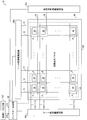
- the stereoscopic image display system 1 includes a liquid crystal display device 10 and shutter glasses 20 (shutter unit).
- the liquid crystal display device 10 includes a liquid crystal display panel 102 that alternately displays a left-eye image and a right-eye image for each frame period by time division.
- the user wears shutter glasses 20 having a left eye shutter that closes and opens the left eye and a right eye shutter that closes and opens the right eye, so that the user can view a stereoscopic image. Can be displayed.
- the stereoscopic video display system of this embodiment includes a liquid crystal display device 10 having a video data output unit 101 and a liquid crystal display panel 102, and a liquid crystal shutter control unit (shutter control unit) 103. And shutter eyeglasses 20 having eyeglasses 111.
- the glasses unit 111 includes a liquid crystal shutter L (left eye shutter) 104 and a liquid crystal shutter R (right eye shutter) 105.
- the video data output unit 101 is a device that sends frame data 106 output as video from the liquid crystal display panel 102 to the liquid crystal display panel 102.
- the video data output unit 101 sequentially transmits left-eye video data and right-eye video data.
- the video data output unit 101 outputs a frame control signal 107 that notifies the frame status at the same time.
- the video data output unit 101 sends a backlight control signal 110 for controlling lighting of the backlight of the liquid crystal display panel 102 to the liquid crystal display panel 102.
- the video data output unit 101 sends data (here, the frame control signal 107) for designating the opening / closing timing of the shutter of the shutter glasses 20 to the liquid crystal shutter control unit 103.
- the liquid crystal display panel 102 displays the frame data 106 output from the video data output unit 101 as a video.
- the liquid crystal shutter control unit 103 controls the OPEN / CLOSE of the liquid crystal shutter L104 and the liquid crystal shutter R105 by the liquid crystal shutter L control signal 108 and the liquid crystal shutter R control signal 109, respectively.
- FIG. 1 shows a state in which the liquid crystal shutter R105 is OPEN (open) and the liquid crystal shutter L104 is CLOSE (closed).
- FIG. 2 shows a state in which the liquid crystal shutter L104 is OPEN (open) and the liquid crystal shutter R105 is CLOSE (closed).
- the liquid crystal shutter L104 of the glasses unit 111 is for use as a left lens of the shutter glasses.
- the liquid crystal shutter L104 includes liquid crystal molecules therein, and the opening / closing of the shutter can be controlled by changing the alignment state of the liquid crystal molecules. That is, when the shutter state is OPEN, the display image of the liquid crystal display panel 102 can be seen by the user's left eye, but when the shutter state is CLOSE, nothing can be seen.
- the liquid crystal shutter R105 of the glasses unit 111 is for use as a right lens of the shutter glasses.
- the liquid crystal shutter R105 also contains liquid crystal molecules, and the opening / closing of the shutter can be controlled by changing the alignment state of the liquid crystal molecules. That is, when the shutter state is OPEN, the display image of the liquid crystal display panel 102 is visible to the user's right eye, but when the shutter state is CLOSE, nothing is visible.
- FIG. 3 is a plan view showing the overall configuration of the liquid crystal display device 10
- FIG. 4 is an equivalent circuit diagram showing one configuration of a pixel P (pixel portion) constituting the liquid crystal display panel 102
- 5 is a plan view showing the configuration of the pixel P.
- the liquid crystal display device 10 includes an active matrix type liquid crystal display panel 102, a source line driving circuit 45s, a gate line driving circuit 45g, a storage capacitor line driving circuit 45c, a video data output unit 101, and a control.
- a circuit 45 is provided.
- the liquid crystal display panel 102 is configured by sandwiching a liquid crystal between an active matrix substrate and a counter substrate, and has a large number of pixels P arranged in a matrix.
- the liquid crystal display panel 102 includes a scanning gate wiring 11a (scanning signal line) and a collective charging gate wiring 11b (first control wiring) on the active matrix substrate.
- FIG. 3 three types of gate wirings 11 a, 11 b, and 11 c are shown as one line, but each gate wiring is actually formed as a separate wiring (see FIGS. 4 and 5).
- the transistors 31, 34, and 35 are shown in FIGS. 4 and 5, but omitted in FIG.
- One source wiring 12 (indicated as 12 (n) and 12 (n + 1) in FIG. 5) is formed in each column so as to be parallel to each other in the column direction (vertical direction), and is a scanning gate.
- One wiring 11a (indicated as 11a (n-1) and 11a (n) in FIG. 5) is formed in each row so as to be parallel to each other in the row direction (lateral direction).
- the transistor 31 and the pixel electrode 30 are formed corresponding to each intersection of the source line 12 (12 (n)) and the scan gate line 11a (11a (n)). Further, the pixel electrode 30 forms a liquid crystal capacitor 32 through the liquid crystal between the counter electrode 14.
- One storage capacitor line 16 is formed in each row so as to be parallel to each other in the row direction (lateral direction), and is arranged to form a pair with the three gate wirings 11a to 11c.
- FIGS. 4 and 5 Specific configuration of pixel P
- the transistor 31 has a source electrode s connected to the source wiring 12 and a gate electrode g connected to the scanning gate wiring 11a.
- the drain electrode d of the transistor 31 is connected to the source electrode s of the transistor 34 and to one electrode 33 b of the storage capacitor 33.
- the transistor 34 has a source electrode s connected to the drain electrode d of the transistor 31 and a gate electrode g connected to the gate wiring 11b for batch charging.
- the drain electrode d of the transistor 34 is connected to the pixel electrode 30 and to the source electrode s of the transistor 35.
- the transistor 35 has a source electrode s connected to the drain electrode d of the transistor 34, a gate electrode g connected to the gate line 11c for collective discharge, and a drain electrode connected to the storage capacitor line 16.
- the pixel electrode 30 forms a liquid crystal capacitor (LC) 32 (first storage capacitor portion) between the counter electrode 14 and the counter electrode 14 via liquid crystal.
- the other electrode 33 a of the storage capacitor 33 is connected to the storage capacitor line 16.
- the storage capacitor 33 constituted by the electrode pairs 33 a and 33 b functions as a capacitor for charging in the pixel for temporarily charging the potential to be applied to the pixel electrode 30 before applying it to the pixel electrode 30.
- the gate of the transistor 31 is temporarily turned on by a gate signal (scanning signal) supplied to the scanning gate wiring 11a and the source signal (data signal) from the source wiring 12 is turned on.
- the held potential is once held in the holding capacitor 33.
- the pixel P is provided with a second transistor 35.
- a gate signal is supplied from the gate wiring 11c to the gate electrode g of the transistor 35 at such a timing that the transistors 35 of all the pixels in the liquid crystal display panel 102 are simultaneously turned on with the transistor 31 turned off. Thereby, each pixel electrode 30 in the liquid crystal display panel 102 can be discharged collectively. Therefore, the transistor 35 is called a collective discharge transistor, and the gate wiring 11c connected to the gate electrode g of the transistor 35 is called a collective discharge gate wiring.
- the pixel P is provided with a third transistor 34.
- the transistor 34 is turned on by a gate signal (control signal) supplied to the gate wiring 11 b and applies the potential held in the holding capacitor 33 to the pixel electrode 30. Accordingly, the pixel electrode 30 is set to a potential corresponding to the source signal, and a voltage corresponding to the source signal is applied to the liquid crystal interposed between the counter electrode 14 and the voltage corresponding to the source signal. Gray scale display can be realized.
- the gate wiring 11b supplies a gate signal at such a timing that the transistors 34 of all the pixels in the liquid crystal display panel 102 are simultaneously turned on. Thereby, each pixel electrode 30 in the liquid crystal display panel 102 can be charged collectively. Therefore, the transistor 34 is called a collective charge transistor, and the gate wiring 11b connected to the gate electrode g of the transistor 34 is called a collective charge gate wiring.
- the liquid crystal display panel 102 configured as described above is driven by a source line driving circuit 45s, a gate line driving circuit 45g, a storage capacitor line driving circuit 45c, and a control circuit 45 for controlling them.
- the horizontal scanning period of each row is sequentially assigned, and each row is sequentially scanned.
- the gate wiring drive circuit 45g sequentially outputs a gate signal for turning on the transistor 31 to the scanning gate wiring 11a of the row in synchronization with the horizontal scanning period (1H) of each row.
- the gate wiring driving circuit 45g applies a gate signal for turning on the transistor 35 to each gate wiring 11c for collective discharge in order to discharge the pixel electrodes 30 of all the pixels P in the liquid crystal display panel 102 at once. Output.
- the gate wiring driving circuit 45g applies a gate signal for turning on the transistor 34 to each gate wiring 11b for batch charging in order to charge the pixel electrodes 30 of all the pixels P in the liquid crystal display panel 102 at once. Output.
- the source wiring drive circuit 45 s outputs a source signal to each source wiring 12.
- the video signal (frame data 106) supplied from the video data output unit 101 to the source wiring driving circuit 45s via the control circuit 45 is assigned to each column in the source wiring driving circuit 45s, and boosted or the like. Signal.
- the storage capacitor line drive circuit 45 c supplies a signal of a constant voltage to each storage capacitor line 16 and fixes the voltage of one electrode 33 a of the storage capacitor 33.
- the control circuit 45 controls the gate wiring driving circuit 45g, the source wiring driving circuit 45s, and the storage capacitor line driving circuit 45c described above based on the video signal (frame data 106) transmitted from the video data output unit 101. Thus, a gate signal, a source signal, and a CS signal are output from each of these circuits.
- the control circuit 45 also controls turning on / off of a backlight (not shown) based on the backlight control signal 110 transmitted from the video data output unit 101.
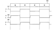
- FIG. 6 shows the relationship between the frame data output to the liquid crystal display panel 102 and the timing of the control signal for controlling the opening / closing of the shutter glasses 20.
- the frame data 106 is video data output to the liquid crystal display panel 102.
- the video data output unit 101 sends out a frame control signal 107 indicating the timing for switching the video for the right eye and the video for the left eye in units of one frame.
- the liquid crystal shutter L104 is set to ON (OPEN) and the liquid crystal shutter R105 is set to OFF (CLOSE), and when the frame control signal 107 is H, an infrared pulse signal is sent, and the liquid crystal shutter controller 103 By switching so that the liquid crystal shutter L104 is turned off and the liquid crystal shutter R105 is turned on when the infrared pulse signal is recognized, the liquid crystal shutter synchronized with the video data can be controlled.
- the liquid crystal shutter L control signal 108 is a signal for controlling OPEN / CLOSE of the liquid crystal shutter L104.
- the liquid crystal shutter R control signal 109 is a signal for controlling OPEN / CLOSE of the liquid crystal shutter R105.
- the frame data 106 and the frame control signal 107 are output from the video data output unit 101.
- the frame data 106 sequentially sends out a right-eye video and a left-eye video.
- the liquid crystal display panel 102 receives the frame data 106 and outputs an image.
- the liquid crystal shutter control unit 103 controls OPEN / CLOSE of the liquid crystal shutter L104 and the liquid crystal shutter R105 based on the frame control signal 107.
- the liquid crystal shutter control unit 103 opens the liquid crystal shutter R105 (the liquid crystal shutter L104 is CLOSE) when the right eye image is displayed on the liquid crystal display panel 102, and opens the liquid crystal shutter L104 when the left eye image is displayed. (Close the liquid crystal shutter R105).
- stereoscopic video can be displayed by the above-described control.
- the video on the liquid crystal display panel is “delayed” for each frame period unique to the liquid crystal display panel that is not included in the CRT display. ”Causes an overlap of pictures in the video for each frame.
- the liquid crystal shutter L control signal 108 and the liquid crystal shutter R control signal 109 L are slightly delayed from the H / L switching timing of the frame control signal 107.
- H (OPEN) To H (OPEN).
- the switching timing (falling) from H (OPEN) to L (CLOSE) in the liquid crystal shutter L control signal 108 and the liquid crystal shutter R control signal 109 are both H / L switching timings of the frame control signal 107. Synchronize with. This allows a period in which both the liquid crystal shutters L and R are CLOSE, so that the user can only have a left-eye video and a right-eye video in which the right-eye video and the left-eye video are not mixed. Displayed, and a good stereoscopic image display is performed.
- the backlight in the H / L switching period of the frame control signal 107 is used. Control may be performed to turn off (extinguish).
- the liquid crystal capacitance 32 of all the pixels in the liquid crystal display panel 102 is controlled by controlling the on / off operation timing of the three transistors 31, 34, and 35 provided in each pixel P.
- the liquid crystal shutter L104 and the liquid crystal shutter R105 are opened are charged and discharged in a single frame. Therefore, even if the period during which the liquid crystal shutter L104 and the liquid crystal shutter R105 are opened is relatively long, it is possible to prevent the right-eye video and the left-eye video from being mixed. Therefore, overlapping of pictures can be suppressed without increasing the frame frequency, and a bright stereoscopic image can be displayed.
- an image based on the previous frame data of the current frame data is displayed on the liquid crystal display panel 102 (that is, the potential of the source signal based on the previous frame data in the liquid crystal capacitor 32 ((g in FIG. 7 In the pixel P, the plurality of gate wirings 11a are sequentially scanned by the gate signal (scanning signal) supplied to the scanning gate wiring 11a while the level A) is held in FIG. Is turned on (see (a) and (b) of FIG. 7).
- a potential corresponding to the source signal (data signal) from the source wiring 12 in the same horizontal scanning period (1H) this is called a data potential.
- FIG. 7E it is indicated by level b).
- the transistor 34 and the transistor 35 are in an off state.
- the data potential is held in the holding capacitor 33 of each pixel P by sequentially operating the plurality of gate wirings 11a (n), 11a (n + 1).
- the transistor 35 is turned on by a gate signal supplied to the collective discharge gate wiring 11c while the transistor 34 is turned off (see FIG. 7D).
- the gate signal supplied to the gate line 11c for collective discharge is applied to the plurality of gate lines 11c at the same timing.
- the charges held in the liquid crystal capacitors 32 in all the pixels P of the liquid crystal display panel 102 are released to the holding capacitor lines 16, and the respective liquid crystal capacitors 32 are discharged together, as shown in FIG.
- the potential of the pixel electrode 30 is a common potential.
- the transistor 35 is turned off while the transistor 31 is turned off, and then the transistor 34 is turned on by a gate signal supplied to the gate wiring 11b for batch charge (see FIG. 7C).
- the gate signal supplied to the gate wiring 11b for batch charging is applied to the plurality of gate wirings 11b at the same timing.
- the potential of the pixel electrode 30 is a potential (eg, level B) based on the data potential (eg, level b).
- the liquid crystal capacitance 32 of each pixel can be charged and discharged collectively in units of one frame (one vertical scanning period: 1 V). Therefore, even if the period during which the liquid crystal shutter L104 and the liquid crystal shutter R105 are opened is relatively long, it is possible to prevent the right-eye video and the left-eye video from being mixed. Therefore, overlapping of pictures can be suppressed without increasing the frame frequency, and a bright stereoscopic image can be displayed.
- the gate signals for collective discharge and collective charge can take sufficient ON time during the retrace period, and are not affected by signal delay when performing collective discharge and collective charge. Therefore, the collective discharge gate line 11c and the collective charge gate line 11b can be made narrower than the scan gate line 11a to suppress a decrease in the aperture ratio (see FIG. 5).
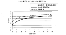
- “C etc.” is a parasitic capacitance with a bus line or the like. Therefore, with respect to the voltage (data voltage) applied to the source s of the transistor 31, in order to obtain sufficient pixel voltage, it is necessary to increase the C 33 with respect to C 32.
- the target of sufficient pixel voltage is the source applied voltage of 7.5 V during white display. 6V.
- C 33 / C 32 is plotted on the horizontal axis, and the pixel voltage Vpx obtained for each capacitance ratio is plotted on the vertical axis. From this, it can be seen that C 33 is required to be approximately four times C 32 in order to obtain the target voltage of 6V.
- the storage capacitor 33 is four times or more the liquid crystal capacitor 32.
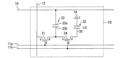
- FIG. 9 shows one configuration of the pixel P2 constituting the liquid crystal display panel 102.
- the collective discharge transistor 35 and the collective discharge gate wiring 11c are not provided in the pixel P2. Since the other configuration is the same as that of the pixel P, the same member numbers as those of the pixel P are given in FIG.
- V 33 and V 32 are in opposite polarity sure. For this reason, when the charging transistor 34 is turned on, the charge Q decreases, so that the pixel voltage decreases. In other words, even if the discharge transistor 35 for forcibly reducing the charge Q is not provided, the polarity is reversed by turning on the charge transistor 34, so that the charge Q is once reduced to a substantially discharged state. can do.
- C 33 is a 8-fold volume of C 32 It is necessary to be. Furthermore, it is desired to further improve the performance of the transistor 31. In addition, in order to suppress the decrease in the aperture ratio due to the increase in transistor size due to high performance, high mobility TFTs such as polysilicon TFTs and transparent oxide semiconductor (IGZO) TFTs are used instead of amorphous silicon TFTs. It is desirable.
- IGZO transparent oxide semiconductor
- the stereoscopic video display system 1 of the present embodiment can be realized by a personal computer.
- the video data output unit 101 is a personal computer
- the liquid crystal display panel 102 is a liquid crystal monitor
- the shutter control unit 103 is configured as an external device.
- the user can view stereoscopic CAD (Computer Aided Design) data and the like.
- CAD Computer Aided Design
- the stereoscopic video display system 1 of the present embodiment can also be implemented by a liquid crystal television.
- the video data output unit 101 is a video output unit inside the liquid crystal television
- the liquid crystal display panel 102 is a liquid crystal panel inside the liquid crystal television
- the liquid crystal shutter control unit 103 is configured as an external device. In this case, viewing of stereoscopically viewable software can be realized on the current home television.
- the present invention does not depend on the liquid crystal mode of the liquid crystal display device to be used, and is typified by a TN mode, a VA mode, an OCB mode, an IPS mode, a horizontal electric field vertical alignment mode for driving a VA liquid crystal by a horizontal electric field, and the like. It can be applied to the nematic liquid crystal mode, chiral liquid crystal such as blue phase, and quasi-isotropic liquid crystal mode.
- the pixel capacity is small in the IPS mode and the horizontal electric field vertical alignment mode, the storage capacity area can be reduced. Therefore, the aperture ratio is increased, and the brightness increasing effect of the present invention can be further enhanced.
- the horizontal electric field vertical alignment mode, OCB mode, chiral liquid crystal, and quasi-isotropic liquid crystal mode have high-speed response, a long shutter opening time can be taken. Therefore, the brightness enhancement effect of the present invention can be further enhanced.
- the display device constituting the stereoscopic video display system of the present invention is not limited to the liquid crystal display device as described above, but can be applied to a display device that performs line sequential scanning such as an organic EL display device. Therefore, hereinafter, a configuration example of a stereoscopic video display system including an organic EL display panel instead of a liquid crystal display panel will be described.
- FIG. 10 shows a configuration of one pixel Pa (pixel unit) constituting the organic EL display panel (display panel).
- FIG. 12 shows a configuration of a pixel Pb of a conventional organic EL display panel for comparison.
- the pixel Pb includes a switching transistor 331 (a first transistor) in the vicinity of an intersection between a scanning gate wiring 311 a and a source wiring (data signal line) 312. Switching element).
- a power supply wiring 317 is provided in parallel with the source wiring 312.
- the pixel Pb includes an organic EL element 332, a driving transistor 336, a storage capacitor 337, a common electrode 314, and the like.
- the source electrode s of the switching transistor 331 is connected to the source wiring 312, the gate electrode g is connected to the gate wiring 311 a, and the drain electrode d is driven with one end of the storage capacitor 337.
- the transistor 336 is connected to the gate electrode g.
- the other end of the storage capacitor 337 is connected to the power supply wiring 317 and the source electrode s of the driving transistor.
- the source electrode s of the driving transistor 336 is connected to the power supply wiring 317, and the anode A of the organic EL element 332 is connected to the drain electrode d.
- the cathode C of the organic EL element 332 is connected to a common electrode 314 formed in the upper layer of the pixel Pb.
- the switching transistor 331 is turned on, so that the charge corresponding to the data signal value supplied to the source wiring 312 passes through the transistor 331 and the driving transistor 336 In addition to being supplied to the gate g, it is supplied and stored in the storage capacitor 337.
- the transistor 331 is turned off, the charge accumulated in the storage capacitor 337 is held.
- the driving transistor 336 by supplying power to the driving transistor 336 from the power supply wiring 317, frame sequential driving can be realized, but the lighting time is limited and the luminance is lowered, which is preferable for display. Absent. Therefore, by continuing to supply power to the power supply wiring 317 during the scanning of the gate wiring 311a, the transistor 336 is kept on, so that the organic EL element 332 continues to emit light by line sequential driving.
- the on-state of the driving transistor 336 is controlled by the charge stored in the storage capacitor 337, the current flowing through the organic EL element 332 is controlled, and the organic EL element 332 emits light with a light emission amount corresponding to the data signal value.
- the configuration of the organic EL display device according to the embodiment of the present invention will be described with reference to FIG.
- the same member number is attached
- the configuration in FIG. 10 includes the gate wiring 311b for collective charging in parallel with the scanning gate wiring 311a (scanning signal line). (First control wiring) is provided.
- the pixel Pa is further provided with a collective charge transistor and a storage capacitor 333 (second storage capacitor unit).
- the source electrode s is connected to the drain electrode d of the transistor 331, and the gate electrode g is connected to the gate wiring 311b for batch charging.
- the drain electrode d of the transistor 334 is connected to the storage capacitor 337 (first storage capacitor portion) and to the gate electrode g of the driving transistor 336.
- one electrode 333 a of the storage capacitor 333 is connected to the drain electrode d of the transistor 331 and the source electrode s of the transistor 334.
- the other electrode 333 b of the storage capacitor 333 is connected to the storage capacitor power source 315.
- the storage capacitor 333 configured by the electrode pairs 333a and 333b is used to temporarily charge a potential to be applied to the storage capacitor 337 for turning on the driving transistor 336 before the storage capacitor 337 is applied. It functions as a capacitor for charging in the pixel. That is, the storage capacitor 333 corresponds to the storage capacitor 33 in the pixel P shown in FIG.
- the collective charging gate wiring 311b supplies a gate signal at a timing at which the transistors 334 of all the pixels Pa in the organic EL display panel are simultaneously turned on. Thereby, the driving transistors 336 in the organic EL display panel can be turned on collectively. That is, the collective charge gate line 311b corresponds to the collective charge gate line 11b in the pixel P shown in FIG. 4, and the collective charge transistor 334 is connected to the collective charge transistor 34 in the pixel P shown in FIG. Equivalent to.
- the configuration and driving method similar to those of the stereoscopic video display system 1 described above can be applied except for the configuration of each pixel Pa described above. Detailed description is omitted.
- the common electrode 314 and the electrode 333b can be connected to the same storage capacitor wiring (not shown in FIG. 10).
- the collective discharge transistor is provided between the gate electrode g of the driving transistor 336 and the storage capacitor wiring.
- the source electrode of the collective discharge transistor may be connected to the gate electrode g of the driving transistor 336, and the drain electrode of the collective discharge transistor may be connected to the storage capacitor wiring.
- the gate electrode of the collective discharge transistor is connected to a collective discharge gate wiring (second control wiring) (not shown in FIG. 10).
- a stereoscopic video display device is a stereoscopic video display device that displays a left-eye video and a right-eye video for performing stereoscopic video display in a time-sharing manner.
- the stereoscopic image display apparatus includes a display panel, and the display panel includes a plurality of data signal lines, a plurality of scanning signal lines intersecting with the plurality of data signal lines, the plurality of data signal lines, and the A pixel unit arranged in a matrix corresponding to each intersection with a plurality of scanning signal lines, and the pixel unit includes a first switching element connected to the scanning signal line and the data signal line A first storage capacitor portion that contributes to display by holding the data potential supplied from the data signal line, and a first storage capacitor portion that holds the data potential before applying it to the first storage capacitor. 2 holding capacity , And a second switching element disposed between the first storage capacitor unit and the second storage capacitor unit, wherein the first switching element scans from the scanning signal line.
- the second switching element is turned on by a signal and applies the data potential supplied from the data signal line to the second storage capacitor portion, and the second switching element is in a period during which the scanning signal line is scanning.
- the display device is characterized in that the video potential displayed on the pixel portion is switched by applying a data potential to the first storage capacitor portion by switching to the on state in the off state.
- the stereoscopic video display device of the present invention is a display device that realizes stereoscopic video display using a shutter glasses method.
- switching is performed with a first storage capacitor portion (corresponding to a liquid crystal capacitor in the case of a liquid crystal display device) provided in a normal liquid crystal display panel in each pixel portion arranged in a matrix.
- the second holding capacitor for temporarily holding the data potential and the first time when the scanning signal line is not scanned (the blanking period) are turned on.
- a switching element (second switching element) that applies a data potential to the storage capacitor portion and switches an image displayed on the pixel portion.
- the second storage capacitor unit that temporarily holds the data potential before being applied to the first storage capacitor unit is provided, so that the current image is displayed in the first storage capacitor unit. While the data potential of the data (current frame) is held and the display based on the data potential is being performed, the next video data (in the second holding capacitor portion of each pixel is scanned by scanning the scanning signal line. The data potential of the next frame) can be charged sequentially.
- the second switching element provided in each pixel is collectively switched from the off state to the on state by using a period in which the scanning signal line is not scanned, so that the first of the pixel portions in the display panel is changed.
- a data potential based on the next video data charged in the second storage capacitor unit can be collectively applied to one storage capacitor unit.
- the first storage capacitor that contributes to the display of each pixel can be charged collectively in units of one piece of video data (one frame), a frame period peculiar to a display panel that performs line sequential scanning. “Delay” of each video is less likely to occur. Therefore, when the display device having the above-described configuration is observed with shutter glasses, the right eye image and the left eye image are mixed even if each of the left eye shutter and the right eye shutter of the shutter glasses is opened for a relatively long time. Can be prevented. Therefore, overlapping of pictures can be suppressed without increasing the frame frequency, and a bright stereoscopic image can be displayed.
- the display panel is a liquid crystal display panel
- the first storage capacitor portion includes a pixel electrode and a counter electrode provided with the liquid crystal of the liquid crystal display panel interposed therebetween. It may be configured to include.
- the mode of the liquid crystal display panel may be any one of an IPS mode, a horizontal electric field vertical alignment mode, a chiral liquid crystal mode, a quasi-isotropic liquid crystal mode, and an OCB mode.
- the display panel is an organic EL display panel having an organic EL display element, and each pixel of the organic EL display panel is for driving for driving the organic EL display element.
- a transistor is further provided, and the first storage capacitor portion may be a storage capacitor for storing a charge corresponding to the data potential supplied to the driving transistor.
- the shutter glasses type stereoscopic image display can be realized in the organic EL display device that performs line sequential scanning.
- Patent Document 4 discloses a technique for realizing three-dimensional image display in an organic EL display panel.
- the display device described in this document is not provided with a capacitor for holding a display (first holding capacitor unit). Therefore, as in the present invention, it is impossible to employ a method of scanning the scanning signal line while displaying an image based on the current video data and supplying the data potential of the next video data to each pixel. .
- the stereoscopic video display device of the present invention may be provided with a first control wiring for controlling on / off of the second switching element.
- the line width of the first control wiring is narrower than the line width of the scanning signal line.
- a decrease in the aperture ratio can be suppressed by reducing the line width of the first control wiring.
- the stereoscopic video display device of the present invention is further provided with a third switching element connected to the first storage capacitor unit and for discharging the charge stored in the first storage capacitor unit. May be.
- the first storage capacitor unit can be forcibly discharged, the data potential supplied from the data signal line is efficiently supplied to the first storage capacitor unit that contributes to display, A target pixel voltage can be obtained. Therefore, the capacity of the second storage capacitor part can be kept relatively small.
- the stereoscopic video display device of the present invention may be provided with a second control wiring for controlling on / off of the third switching element.
- the line width of the second control wiring is narrower than the line width of the scanning signal line.
- the first switching element is preferably a transparent oxide semiconductor TFT or a polysilicon TFT.
- a stereoscopic video display system corresponds to any one of the above-described stereoscopic video display devices, a left-eye video, and a right-eye video. And a shutter unit that selectively transmits each image to the right eye.
- the stereoscopic video display system of the present invention realizes stereoscopic video display using the shutter glasses method. Since the stereoscopic video display system of the present invention includes the stereoscopic video display device of the present invention, a bright stereoscopic video can be displayed without increasing the frame frequency. Accordingly, an observer who visually recognizes an image using the shutter unit can see a stereoscopic image that is bright and does not overlap the left and right images.
- the shutter unit may be glasses.
- a driving method of a stereoscopic video display device is a driving method of a stereoscopic video display device according to the present invention, wherein a current out of a plurality of video data displayed in the time-division manner on the first holding capacitor. While the data potential based on the video data is held, the first switching element is turned on while the second switching element is turned off, and the time is displayed on the second holding capacitor in the time division manner. And charging the data potential based on the next video data of the plurality of video data to be turned on, and turning on the second switching element in each pixel in a state where the first switching element is turned off. As a result, the data potential based on the next video data charged in the second storage capacitor is collectively applied to the first storage capacitor of each pixel, and display based on the data potential is performed. Characterized in that it comprises a and.
- the second storage capacitor unit that temporarily holds the data potential before being applied to the first storage capacitor unit is provided, so that the current image is displayed in the first storage capacitor unit. While the data potential of the data (current frame) is held and the display based on the data potential is being performed, the next video data (in the second holding capacitor portion of each pixel is scanned by scanning the scanning signal line. The data potential of the next frame) can be charged sequentially.
- the second switching element provided in each pixel is collectively switched from the off state to the on state using a period in which the scanning signal line is not scanned, so that the second switching element of each pixel portion in the display panel is switched.
- a data potential based on the next video data charged in the second storage capacitor unit can be collectively applied to one storage capacitor unit.
- the first storage capacitor that contributes to the display of each pixel can be charged collectively in units of one piece of video data (one frame), a frame period peculiar to a display panel that performs line sequential scanning. “Delay” of each video is less likely to occur. Therefore, when observing the image displayed by the above method with the shutter glasses, the right-eye image and the left-eye image can be obtained even if each of the left eye shutter and the right eye shutter of the shutter glasses has a relatively long open time. Can be prevented. Therefore, overlapping of pictures can be suppressed without increasing the frame frequency, and a bright stereoscopic image can be displayed.
- the stereoscopic video display device driving method according to the present invention is a stereoscopic video display device driving method according to the present invention, wherein the current data among the plurality of video data displayed in the time-division manner is displayed in the first storage capacitor. While the data potential based on the video data is held, the first switching element is turned on while the second switching element and the third switching element are turned off, and the second holding capacitor is turned on. In addition, a step of charging a data potential based on the next video data among the plurality of video data displayed in a time-sharing manner, and the second switching element in an off state while collectively turning on the first data in each pixel.
- the second storage capacitor unit that temporarily holds the data potential before being applied to the first storage capacitor unit is provided, so that the current image is displayed in the first storage capacitor unit. While the data potential of the data (current frame) is held and the display based on the data potential is being performed, the next video data (in the second holding capacitor portion of each pixel is scanned by scanning the scanning signal line. The data potential of the next frame) can be charged sequentially.
- the third switching element for discharge provided in each pixel is collectively switched from the off state to the on state, whereby each pixel in the display panel.
- the discharge of the data potential based on the current video data can be performed collectively.
- the third switching elements in the on state are collectively turned off, and the second switching elements provided in each pixel are collectively turned off.
- a data potential based on the next video data charged in the second storage capacitor unit is applied to the first storage capacitor unit of each pixel unit in the display panel at once. Can do.
- the present invention can be applied to a display device and a display system that perform stereoscopic display (3D display).
- Liquid crystal display device (display device) 11a (for scanning) gate wiring (scanning signal line) 11b Gate wiring (for batch charging) (first control wiring) 11c (for collective discharge) gate wiring (second control wiring) 12 Source wiring (data signal line) 14 Counter electrode (first holding capacitor) 16 Retention capacity line 20 Shutter glasses (shutter part) 30 pixel electrode (first storage capacitor) 31 transistor (first switching element) 32 Liquid crystal capacitor (first holding capacitor) 33 Retention capacity (second retention capacity part) 34 Collective charge transistor (second switching element) 35 Collective discharge transistor (third switching element) 101 video data output unit 102 liquid crystal display panel (display panel) 103 Liquid crystal shutter controller (shutter controller) 104 Liquid Crystal Shutter L (Left Eye Shutter) 105 Liquid crystal shutter R (Right-eye shutter) 106 Frame data 107 Frame control signal 108 Liquid crystal shutter L control signal 109 Liquid crystal shutter R control signal 111 Glasses 311a Gate wiring (scanning signal line)
Landscapes
- Engineering & Computer Science (AREA)
- Physics & Mathematics (AREA)
- General Physics & Mathematics (AREA)
- Computer Hardware Design (AREA)
- Theoretical Computer Science (AREA)
- Multimedia (AREA)
- Signal Processing (AREA)
- Chemical & Material Sciences (AREA)
- Crystallography & Structural Chemistry (AREA)
- Optics & Photonics (AREA)
- Control Of Indicators Other Than Cathode Ray Tubes (AREA)
- Testing, Inspecting, Measuring Of Stereoscopic Televisions And Televisions (AREA)
Abstract
本発明の液晶表示装置(10)は、マトリクス状に配置された画素Pを備えている。画素Pには、ソース配線(12)から供給されるデータ電位が印加される画素電極(30)と、上記データ電位を画素電極(30)に印加する前に一旦保持しておく保持容量(33)と、スキャン用のゲート配線(11a)およびソース配線(12)に接続されており、ソース配線(12)から供給されるデータ電位を保持容量(33)に印加するためのトランジスタ(31)と、保持容量(33)と画素電極(30)との間に配置され、保持容量(33)に一旦印加されたデータ電位を画素電極(30)に印加するための一括充電用トランジスタ(34)と、画素電極(30)に接続されており、該画素電極の放電を行うための一括放電用トランジスタ(35)とが設けられている。これにより、フレーム周波数を上げることなく明るい立体映像を表示することのできるシャッタ眼鏡方式の液晶表示装置を実現する。
Description
本発明は、左眼用映像と右眼用映像とを時分割によりフレーム期間ごとに交互に表示することで立体映像を表示する立体映像表示装置、およびこの立体映像表示装置を有する立体映像表示システムに関するものである。
近年、フラットパネルディスプレイとして、液晶ディスプレイ等の需要が急速に伸びている。液晶ディスプレイは、CRT(Cathode Ray Tube)ディスプレイに比べて、消費電力が少なく、小型化がしやすいため、テレビをはじめ、携帯電話、携帯型ゲーム機、車載用ナビゲーション装置などに幅広く利用されている。
ところで、昨今、各種表示装置において、立体表示(3D表示)を可能とする映像表示技術が提案されている。例えば、CRTディスプレイにおいては、左眼用映像と右眼用映像とを時分割によりフレーム期間ごとに交互に表示し、ユーザが、左眼及び右眼をそれぞれ閉鎖及び開放する左眼用シャッタ及び右眼用シャッタを有するシャッタ眼鏡を着用することにより、ユーザに立体映像を表示する技術が提案されている。
また、液晶表示装置においても、上記のシャッタ眼鏡を用いた立体映像表示技術を応用した映像表示方法が提案されている(特許文献1および2参照)。
例えば、特許文献1では、液晶ディスプレイが表示する左眼用映像及び右眼用映像の各フレーム期間のうち、液晶ディスプレイの垂直ブランキング期間における左眼用映像のみが左眼に表示され、液晶ディスプレイの垂直ブランキング期間における右眼用映像のみが右眼に表示されるように、シャッタ眼鏡の開閉を行うという方法が提案されている。これにより、ユーザに対して左眼用映像と右眼用映像とが混在した映像が表示されてしまうという、いわゆるクロストークの問題を解消している。この点について、以下に説明する。
図11には、特許文献1に記載の方法でシャッタ眼鏡の開閉を制御した場合のタイミングチャートを示す。
図11において、206は、左眼用映像(Leftn)と右眼用映像(Rightn)とを時分割によりフレーム期間ごとに交互に表示する液晶ディスプレイに出力される映像データを模式的に示したものである。また、この液晶ディスプレイには、左眼を閉鎖及び開放する液晶シャッタL(左眼用シャッタ)と、右眼を閉鎖及び開放する液晶シャッタR(右眼用シャッタ)とを有するシャッタ眼鏡と、シャッタ眼鏡の液晶シャッタL及びRの閉鎖及び開放をそれぞれ制御する液晶シャッタ制御部とが備えられている。図11には、液晶シャッタLの開閉を制御するための液晶シャッタL制御信号208のタイミングチャートと、液晶シャッタRの開閉を制御するための液晶シャッタR制御信号209のタイミングチャートとを示す。
図11に示すように、実際の液晶ディスプレイの各々のフレーム期間には、垂直同期信号に従って、実際に画素データを送り出している期間である重複期間501,502,503と、次のフレーム期間の開始まで画素データの送出を中止している期間である垂直ブランキング期間504とが存在する。重複期間501,502,503においては、あるフレーム期間の映像(例えば、左眼用映像Left1)が、その次のフレーム期間の映像(例えば、右眼用映像Right1)に書き換えられるため、前後のフレーム期間同士の映像が重なっているように見える。一方、垂直ブランキング期間504においては、各々同士の画像が混在していない左眼用映像及び右眼用映像のみが表示されることになる。
このように、液晶ディスプレイにおいて、重複期間501,502,503が存在するため、単にフレーム期間ごとに左眼用シャッタ及び右眼用シャッタを交互に開閉しているだけでは、ユーザには、右眼用映像と左眼用映像とが重なった表示映像が目に入ってしまい、立体視することができない。
そこで、特許文献1の方法では、図11に示すように、液晶シャッタ制御部は、液晶ディスプレイが表示する左眼用映像及び右眼用映像のそれぞれのフレーム期間のうちで、液晶ディスプレイの垂直ブランキング期間504のみ、シャッタ眼鏡の液晶シャッタL及びRに、左眼及び右眼のそれぞれを開放させるという制御を行っている。
これにより、ユーザには、右眼用映像と左眼用映像とが混在していない左眼用映像及び右眼用映像のみが表示され、液晶ディスプレイによる立体映像表示が可能となる。
しかしながら、垂直ブランキング期間のみシャッタ眼鏡を開放するという上記の方法では、左眼用映像及び右眼用映像のそれぞれについて、全フレーム期間の約1/4の期間のみしか液晶シャッタが開放されない。また、フルハイビジョンTV信号では伝送速度の制約などから、さらに開放時間が短くなり、最大でも全フレーム期間の15%、現実的には4%程度のみしか液晶シャッタが開放されない。そのため、画面全体が暗くなってしまい、表示される立体映像が見難くなるという問題が生ずる。
なお、特許文献2に記載の映像表示方法では、上記の問題に対処するために、左眼用映像の表示期間において第1左眼用フレームL1と、第1左眼用フレームL1と同じ映像の第2左眼用フレームL2を順次表示し、右眼用映像の表示期間において第1右眼用フレームR1と、第1右眼用フレームR1と同じ映像の第2右眼用フレームR2を順次表示している。このように、右眼用映像及び左眼用映像の表示期間において、同じ映像のフレームを2度続けて表示することにより、右眼用映像及び左眼用映像のフレームが確定している時間を延ばすことができるため、表示される立体画像を見易いものとすることが可能となると記載されている。
しかしながら、動画映像において上記のような表示駆動を行う場合には、フレーム周波数が240Hz程度の高速駆動を行わなければ、シャッタのON/OFFの点滅(フリッカ)が視認されてしまい表示品位が損なわれる。このような高速駆動は、駆動回路に大きな負荷をかけ、またコストも上がることになり望ましくない。
また、特許文献1に比べて液晶シャッタの開放期間が延びるとは言え、原理的に全フレーム期間の約1/2程度しか開放することはできない。
本発明は、上記の問題点に鑑みてなされたものであり、フレーム周波数を上げることなく明るい立体映像を表示することのできるシャッタ眼鏡方式の立体映像表示装置、および立体映像表示システムを提供することを目的とする。
本発明にかかる立体映像表示装置は、上記の課題を解決するために、立体映像表示を行うための左眼用の映像及び右眼用の映像を、時分割で表示する立体映像表示装置であって、上記立体映像表示装置は、表示パネルを含み、上記表示パネルは、複数のデータ信号線と、これら複数のデータ信号線と交差する複数の走査信号線と、上記複数のデータ信号線と上記複数の走査信号線との各交点に対応してマトリクス状に配置された画素部とを備えており、上記画素部は、上記走査信号線および上記データ信号線に接続された第1のスイッチング素子と、上記データ信号線から供給されるデータ電位を保持することで表示に寄与する第1の保持容量部と、上記データ電位を上記第1の保持容量に印加する前に一旦保持しておく第2の保持容量部と、上記第1の保持容量部と第2の保持容量部との間に配置された第2のスイッチング素子とを、有しており、上記第1のスイッチング素子は、上記走査信号線からの走査信号によってオン状態となり、上記データ信号線から供給されたデータ電位を上記第2の保持容量部に印加するものであり、上記第2のスイッチング素子は、上記走査信号線が走査している期間はオフ状態にあり、オン状態に切り替わることで、上記第1の保持容量部にデータ電位を印加して、上記画素部に表示される映像を切り替えるものであることを特徴とする。
本発明の立体映像表示装置は、シャッタ眼鏡方式を用いて立体映像表示を実現する表示装置である。本発明の表示装置には、マトリクス状に配置された各画素部内に、通常の液晶表示パネルに設けられている第1の保持容量部(液晶表示装置の場合には液晶容量に相当)とスイッチング素子(第1のスイッチング素子)に加え、データ電位を一旦保持するための第2の保持容量と、走査信号線が走査していない期間(帰線期間)にオンされることで、第1の保持容量部にデータ電位を印加して、画素部に表示される映像を切り替えるスイッチング素子(第2のスイッチング素子)とが備えられている。
上記の構成によれば、データ電位を第1の保持容量部に印加する前に一旦保持しておく第2の保持容量部が設けられていることで、第1の保持容量部に現在の映像データ(現フレーム)のデータ電位が保持され、このデータ電位に基づく表示が行われている間に、走査信号線を走査することで、各画素の第2の保持容量部に次の映像データ(次フレーム)のデータ電位を順次充電することができる。
そして、走査信号線が走査していない期間を利用して、各画素に設けられた第2のスイッチング素子を一括してオフ状態からオン状態へ切り替えることで、表示パネル内の各画素部の第1の保持容量部に、第2の保持容量部に充電されていた次の映像データに基づくデータ電位を一括して印加することができる。
これにより、1枚の映像データ(1フレーム)単位で一括して各画素の表示に寄与する第1の保持容量部の充電を行うことができるため、線順次走査を行う表示パネル特有のフレーム期間ごとの映像の「遅延」が発生しにくくなる。したがって、上記構成の表示装置をシャッタ眼鏡で観察するときに、シャッタ眼鏡の左眼用シャッタおよび右眼用シャッタの各開放時間を比較的長くとっても、右眼用映像と左眼用映像との混在を防ぐことができる。そのため、フレーム周波数を上げることなく絵の重なりを抑え、明るい立体映像を表示することができる。
本発明にかかる立体映像表示システムは、上記の課題を解決するために、上記の立体映像表示装置と、左眼用の映像と右眼用の映像のそれぞれに対応して、左眼および右眼にそれぞれ各映像を選択的に透過させるシャッタ部とを備えている。
本発明の立体映像表示システムは、シャッタ眼鏡方式を用いて立体映像表示を実現するものである。本発明の立体映像表示システムは、本発明の立体映像表示装置を備えているため、フレーム周波数を上げることなく明るい立体映像を表示することができる。したがって、シャッタ部を用いて映像を視認する観察者は、明るく、左右の映像が重なることのない立体映像を見ることができる。
本発明にかかる立体映像表示装置の駆動方法は、本発明の立体映像表示装置の駆動方法であって、上記第1の保持容量に、上記時分割で表示される複数の映像データのうちの現在の映像データに基づくデータ電位が保持されている間に、上記第2のスイッチング素子をオフした状態で、上記第1のスイッチング素子をオンし、上記第2の保持容量に、上記時分割で表示される複数の映像データのうちの次の映像データに基づくデータ電位を充電する工程と、上記第1のスイッチング素子をオフした状態で、各画素において一括して上記第2のスイッチング素子をオンすることで、上記第2の保持容量に充電された上記次の映像データに基づくデータ電位を各画素の上記第1の保持容量に一括して印加し、該データ電位に基づく表示を行う工程と、を含むことを特徴とする。
上記の方法によれば、データ電位を第1の保持容量部に印加する前に一旦保持しておく第2の保持容量部が設けられていることで、第1の保持容量部に現在の映像データ(現フレーム)のデータ電位が保持され、このデータ電位に基づく表示が行われている間に、走査信号線を走査することで、各画素の第2の保持容量部に次の映像データ(次フレーム)のデータ電位を順次充電することができる。
そして、走査信号線が走査していない期間を利用して、各画素に設けられた第2のスイッチング素子を一括してオフ状態からオン状態へ切り替えることで、表示パネル内の各画素部の第1の保持容量部に、第2の保持容量部に充電されていた次の映像データに基づくデータ電位を一括して印加することができる。
これにより、1枚の映像データ(1フレーム)単位で一括して各画素の表示に寄与する第1の保持容量部の充電を行うことができるため、線順次走査を行う表示パネル特有のフレーム期間ごとの映像の「遅延」が発生しにくくなる。したがって、上記方法で表示された映像をシャッタ眼鏡で観察するときに、シャッタ眼鏡の左眼用シャッタおよび右眼用シャッタの各開放時間を比較的長くとっても、右眼用映像と左眼用映像との混在を防ぐことができる。そのため、フレーム周波数を上げることなく絵の重なりを抑え、明るい立体映像を表示することができる。
本発明の立体映像表示装置、および立体映像表示システムによれば、フレーム周波数を上げることなく絵の重なりを抑え、明るい立体映像を表示することができる。
本発明の一実施形態について図1~図10に基づいて説明すると以下の通りである。なお、本発明はこれに限定されるものではない。
本実施の形態では、シャッタ眼鏡方式を用いて立体映像表示を行う液晶表示装置(表示装置)、および、該液晶表示装置とシャッタ眼鏡とで構成される立体映像表示システムについて、説明する。ここで、シャッタ眼鏡方式の立体映像表示技術とは、左眼用映像と右眼用映像とを時分割によりフレーム期間ごとに交互に表示し、ユーザが、左眼及び右眼をそれぞれ閉鎖及び開放する左眼用シャッタ及び右眼用シャッタを有するシャッタ眼鏡を着用することにより、ユーザに立体映像を表示する技術のことである。
(立体映像表示システムの構成について)
図1及び図2は、本実施の形態にかかる立体映像表示システムの構成例を示す図であり、それぞれ液晶シャッタL、液晶シャッタRを閉鎖している状態を示す図である。本実施形態の立体映像表示システム1は、液晶表示装置10とシャッタ眼鏡20(シャッタ部)とで構成されている。液晶表示装置10は、左眼用映像と右眼用映像とを時分割によりフレーム期間ごとに交互に表示する液晶表示パネル102を有している。この液晶表示パネル102では、ユーザが、左眼を閉鎖及び開放する左眼用シャッタと、右眼を閉鎖及び開放する右眼用シャッタとを有するシャッタ眼鏡20を着用することにより、ユーザに立体映像を表示することができる。
図1及び図2は、本実施の形態にかかる立体映像表示システムの構成例を示す図であり、それぞれ液晶シャッタL、液晶シャッタRを閉鎖している状態を示す図である。本実施形態の立体映像表示システム1は、液晶表示装置10とシャッタ眼鏡20(シャッタ部)とで構成されている。液晶表示装置10は、左眼用映像と右眼用映像とを時分割によりフレーム期間ごとに交互に表示する液晶表示パネル102を有している。この液晶表示パネル102では、ユーザが、左眼を閉鎖及び開放する左眼用シャッタと、右眼を閉鎖及び開放する右眼用シャッタとを有するシャッタ眼鏡20を着用することにより、ユーザに立体映像を表示することができる。
図1及び図2に示すように、本実施形態の立体映像表示システムは、映像データ出力部101と、液晶表示パネル102とを有する液晶表示装置10と、液晶シャッタ制御部(シャッタ制御部)103と、眼鏡部111とを有するシャッタ眼鏡20とで構成される。眼鏡部111は、液晶シャッタL(左眼用シャッタ)104および液晶シャッタR(右眼用シャッタ)105を有している。
映像データ出力部101は、液晶表示パネル102から映像として出力されるフレームデータ106を液晶表示パネル102に送り出す装置である。本実施形態では、映像データ出力部101は、左眼用の映像データ、右眼用の映像データを順番に送出する。映像データ出力部101は、同時にフレームのステータスを知らせるフレーム制御信号107を出力する。さらに、映像データ出力部101は、液晶表示パネル102のバックライトの点灯を制御するバックライト制御信号110を液晶表示パネル102に送出する。加えて、映像データ出力部101は、液晶シャッタ制御部103に対し、シャッタ眼鏡20のシャッタの開閉のタイミングを指定するためのデータ(ここでは、フレーム制御信号107)を送出する。
液晶表示パネル102は、映像データ出力部101より出力されたフレームデータ106を映像として表示する。
液晶シャッタ制御部103は、液晶シャッタL104、液晶シャッタR105を、それぞれ液晶シャッタL制御信号108及び液晶シャッタR制御信号109により、それらのOPEN/CLOSE(開閉)を制御する。図1では、液晶シャッタR105がOPEN(開)であり、液晶シャッタL104がCLOSE(閉)である状態を示している。一方、図2では、液晶シャッタL104がOPEN(開)であり、液晶シャッタR105がCLOSE(閉)である状態を示している。
眼鏡部111の液晶シャッタL104は、シャッタ眼鏡の左側のレンズとして使用されるためのものである。この液晶シャッタL104には、内部に液晶分子が含まれており、この液晶分子の配向状態を変更することによって、シャッタの開閉を制御することができる。すなわち、シャッタ状態がOPENのときには、ユーザの左眼には、液晶表示パネル102の表示映像が見えるが、シャッタ状態がCLOSEのときには何も見えないようになっている。
眼鏡部111の液晶シャッタR105は、シャッタ眼鏡の右側のレンズとして使用されるためのものである。この液晶シャッタR105にも、内部に液晶分子が含まれており、この液晶分子の配向状態を変更することによって、シャッタの開閉を制御することができる。すなわち、シャッタ状態がOPENのときには、ユーザの右眼には、液晶表示パネル102の表示映像が見えるが、シャッタ状態がCLOSEのときには何も見えないようになっている。
(液晶表示装置の構成について)
ここで、液晶表示装置10およびその内部に備えられた液晶表示パネル102のより具体的な構成について、図3、図4、および図5を参照しながら説明する。図3は、液晶表示装置10の全体構成を示す平面図であり、図4は、液晶表示パネル102を構成している画素P(画素部)の一つの構成を示す等価回路図であり、図5は、画素Pの構成を示す平面図である。
ここで、液晶表示装置10およびその内部に備えられた液晶表示パネル102のより具体的な構成について、図3、図4、および図5を参照しながら説明する。図3は、液晶表示装置10の全体構成を示す平面図であり、図4は、液晶表示パネル102を構成している画素P(画素部)の一つの構成を示す等価回路図であり、図5は、画素Pの構成を示す平面図である。
図3に示すように、液晶表示装置10は、アクティブマトリクス型の液晶表示パネル102、ソース配線駆動回路45s、ゲート配線駆動回路45g、保持容量線駆動回路45c、映像データ出力部101、及び、コントロール回路45を備えている。
液晶表示パネル102は、アクティブマトリクス基板と対向基板との間に液晶を挟持して構成されており、マトリクス状に配列された多数の画素Pを有している。
そして、図4および図5に示すように、液晶表示パネル102は、アクティブマトリクス基板上に、スキャン用のゲート配線11a(走査信号線)、一括充電用のゲート配線11b(第1の制御配線)、一括放電用のゲート配線11c(第2の制御配線)、ソース配線(データ信号線)12、スイッチング素子であるトランジスタ31(第1のスイッチング素子)・トランジスタ34(第2のスイッチング素子)・トランジスタ35(第3のスイッチング素子)、画素電極30、及び保持容量線16(CS配線とも呼ぶ)を備え、対向基板上に対向電極14を備えている。なお、図3では、3種類のゲート配線11a・11b・11cを一本で示しているが、実際は、それぞれのゲート配線が別個の配線で形成されている(図4および図5参照)。また、トランジスタ31・34・35は、図4および図5では図示しているが、図3では省略している。
ソース配線12(図5では、12(n)、12(n+1)と記載)は、列方向(縦方向)に互いに平行となるように各列に1本ずつ形成されており、スキャン用のゲート配線11a(図5では、11a(n-1)、11a(n)と記載)は、行方向(横方向)に互いに平行となるように各行に1本ずつ形成されている。トランジスタ31及び画素電極30は、ソース配線12(12(n))とスキャン用のゲート配線11a(11a(n))との各交点に対応してそれぞれ形成されている。また、画素電極30は、対向電極14との間に液晶を介して液晶容量32を形成している。保持容量線16は、行方向(横方向)に互いに平行となるように各行に1本ずつ形成されており、3本のゲート配線11a~cと対をなすように配置されている。
(画素Pの具体的な構成について)
続いて、一画素Pのより具体的な構成について、図4および図5を参照しながら説明する。図4および図5に示すように、画素P内には、3つのトランジスタ31・34・35と、液晶容量32(第1の保持容量部)を形成するための画素電極30および対向電極14と、保持容量33(第2の保持容量部)を形成するための保持容量電極対33a・33bとが設けられている。
続いて、一画素Pのより具体的な構成について、図4および図5を参照しながら説明する。図4および図5に示すように、画素P内には、3つのトランジスタ31・34・35と、液晶容量32(第1の保持容量部)を形成するための画素電極30および対向電極14と、保持容量33(第2の保持容量部)を形成するための保持容量電極対33a・33bとが設けられている。
トランジスタ31は、そのソース電極sがソース配線12に、ゲート電極gがスキャン用のゲート配線11aにそれぞれ接続されている。また、トランジスタ31のドレイン電極dは、トランジスタ34のソース電極sに接続されているとともに、保持容量33の一方の電極33bに接続されている。
トランジスタ34は、そのソース電極sがトランジスタ31のドレイン電極dに、ゲート電極gが一括充電用のゲート配線11bにそれぞれ接続されている。また、トランジスタ34のドレイン電極dは、画素電極30に接続されているとともに、トランジスタ35のソース電極sに接続されている。
トランジスタ35は、そのソース電極sがトランジスタ34のドレイン電極dに、ゲート電極gが一括放電用のゲート配線11c、ドレイン電極が保持容量線16にそれぞれ接続されている。
また、画素電極30は、対向電極14との間に液晶を介して液晶容量(LC)32(第1の保持容量部)を形成している。さらに、保持容量33の他方の電極33aは、保持容量線16に接続されている。電極対33a・33bで構成される保持容量33は、画素電極30に印加すべき電位を、画素電極30に印加する前に一旦充電しておくための画素内充電用のキャパシタとして機能する。
上記のような構成を有する画素Pでは、スキャン用のゲート配線11aに供給されるゲート信号(走査信号)によってトランジスタ31のゲートを一旦オンし、ソース配線12からのソース信号(データ信号)に応じた電位を、一旦保持容量33に保持する。
また、画素Pには2つ目のトランジスタ35が設けられている。このトランジスタ35のゲート電極gには、トランジスタ31をオフにした状態で、液晶表示パネル102内の全画素のトランジスタ35が同時にオンするようなタイミングでゲート配線11cからゲート信号が供給される。これにより、液晶表示パネル102内の各画素電極30を一括して放電することができる。そのため、トランジスタ35を一括放電用トランジスタと呼び、また、トランジスタ35のゲート電極gに接続されたゲート配線11cを一括放電用のゲート配線と呼ぶ。
さらに、画素Pには3つ目のトランジスタ34が設けられている。このトランジスタ34は、ゲート配線11bに供給されるゲート信号(制御信号)によってオンとなり、保持容量33に保持された電位を画素電極30に印加する。これにより、画素電極30を上記ソース信号に応じた電位に設定し、対向電極14との間に介在する液晶に対して上記ソース信号に応じた電圧を印加することによって、上記ソース信号に応じた階調表示を実現することができる。
なお、ゲート配線11bは、液晶表示パネル102内の全画素のトランジスタ34が同時にオンするようなタイミングでゲート信号を供給する。これにより、液晶表示パネル102内の各画素電極30を一括して充電することができる。そのため、トランジスタ34を、一括充電用トランジスタと呼び、また、トランジスタ34のゲート電極gに接続されたゲート配線11bを一括充電用のゲート配線と呼ぶ。
なお、画素Pにおける各トランジスタ31・34・35のオン/オフの動作タイミングについては、後述する。
(液晶表示装置10内の各種回路について)
上記構成の液晶表示パネル102は、ソース配線駆動回路45s、ゲート配線駆動回路45g、保持容量線駆動回路45c、及びこれらを制御するコントロール回路45によって駆動される。
上記構成の液晶表示パネル102は、ソース配線駆動回路45s、ゲート配線駆動回路45g、保持容量線駆動回路45c、及びこれらを制御するコントロール回路45によって駆動される。
本実施形態では、周期的に繰り返される垂直走査期間におけるアクティブ期間(有効走査期間)において、各行の水平走査期間を順次割り当て、各行を順次走査していく。
そのために、ゲート配線駆動回路45gは、トランジスタ31をオンするためのゲート信号を各行の水平走査期間(1H)に同期して当該行のスキャン用のゲート配線11aに対して順次出力する。
また、ゲート配線駆動回路45gは、液晶表示パネル102内の全画素Pの画素電極30を一括して放電するために、トランジスタ35をオンするためのゲート信号を一括放電用の各ゲート配線11cに対して出力する。
さらに、ゲート配線駆動回路45gは、液晶表示パネル102内の全画素Pの画素電極30を一括して充電するために、トランジスタ34をオンするためのゲート信号を一括充電用の各ゲート配線11bに対して出力する。
また、ソース配線駆動回路45sは、各ソース配線12に対してソース信号を出力する。このソース信号は、映像データ出力部101からコントロール回路45を介してソース配線駆動回路45sに供給された映像信号(フレームデータ106)を、ソース配線駆動回路45sにおいて各列に割り当て、昇圧等を施した信号である。
また、保持容量線駆動回路45cは、各保持容量線16に一定の電圧の信号を供給し、保持容量33の一方の電極33aの電圧を固定する。
コントロール回路45は、映像データ出力部101から送信された映像信号(フレームデータ106)に基づいて、上述したゲート配線駆動回路45g、ソース配線駆動回路45s、及び保持容量線駆動回路45cを制御することにより、これら各回路から、ゲート信号、ソース信号、及びCS信号を出力させるものである。また、コントロール回路は45は、映像データ出力部101から送信されたバックライト制御信号110に基づいて、バックライト(図示せず)の点灯及び消灯の制御も行う。
(フレームデータとシャッタ眼鏡の開閉タイミングとの関係について)
以下には、液晶表示パネル102に出力されるフレームデータと、シャッタ眼鏡20の開閉のタイミングとの関係について説明する。
以下には、液晶表示パネル102に出力されるフレームデータと、シャッタ眼鏡20の開閉のタイミングとの関係について説明する。
図6には、液晶表示パネル102に出力されるフレームデータと、シャッタ眼鏡20の開閉を制御する制御信号のタイミングとの関係を示す。フレームデータ106は、液晶表示パネル102に出力する映像データである。本実施形態において、映像データ出力部101は、右眼用の映像、左眼用の映像を切り替えるタイミングを示すフレーム制御信号107を1フレーム単位で送り出す。
フレーム制御信号107は、フレームデータ106のステータスを示すものである。図6に示すように、本実施形態においては、映像データ出力部101は、左眼用のフレームデータ106の出力時にフレーム制御信号107=Lを出力し、右眼用のフレームデータ106の出力時にフレーム制御信号107=Hを出力する。映像データ出力部101から出力されたフレーム制御信号107は、シャッタ眼鏡20内に備えられた液晶シャッタ制御部103に送信される。
具体的には、通常状態で液晶シャッタL104をON(OPEN)、液晶シャッタR105をOFF(CLOSE)の状態に設定し、フレーム制御信号107がHの時に赤外線パルス信号を送り、液晶シャッタ制御部103がこの赤外線パルス信号を認識した時に液晶シャッタL104がOFF、液晶シャッタR105がONとなるように切り替えることで、映像データに同期した液晶シャッタの制御が可能となる。
液晶シャッタL制御信号108は、液晶シャッタL104のOPEN/CLOSEを制御するための信号である。液晶シャッタR制御信号109は、液晶シャッタR105のOPEN/CLOSEを制御するための信号である。これらの信号パターンについては後述する。
以下、本実施形態の立体映像表示装置の動作について説明する。本実施形態では、映像データ出力部101よりフレームデータ106とフレーム制御信号107を出力する。フレームデータ106は、右眼用の映像、左眼用の映像を順番に送り出す。液晶表示パネル102は、フレームデータ106を受け取ることで映像を出力する。
液晶シャッタ制御部103はフレーム制御信号107を元に、液晶シャッタL104、液晶シャッタR105のOPEN/CLOSEを制御する。液晶シャッタ制御部103は、液晶表示パネル102に右眼用の映像が出ているときには液晶シャッタR105をOPEN(液晶シャッタL104をCLOSE)、左眼用の映像が出ているときには液晶シャッタL104をOPEN(液晶シャッタR105をCLOSE)する。
基本的には、上記のような制御により立体映像を表示することができるようになるが、液晶表示パネルにおける映像には、CRTディスプレイには無い液晶表示パネル特有のフレーム期間ごとの映像の「遅延」により、フレームごとの映像に絵の重なりが発生する。
そこで、本実施の形態では、図6に示すように、フレーム制御信号107のH/Lの切り替えのタイミングから少し遅延して、液晶シャッタL制御信号108および液晶シャッタR制御信号109のL(CLOSE)からH(OPEN)への切り替えが行われる。また、液晶シャッタL制御信号108および液晶シャッタR制御信号109における、H(OPEN)からL(CLOSE)への切り替わり(立ち下がり)のタイミングはともに、フレーム制御信号107のH/Lの切り替えのタイミングと同期している。これにより、液晶シャッタLおよびRがともにCLOSEとなるような期間ができるため、ユーザには、右眼用映像と左眼用映像とが混在していない左眼用映像及び右眼用映像のみが表示され、良好な立体映像表示が行われる。
なお、上記のように、液晶シャッタで右/左ともにCLOSEとなる期間を作るようにシャッタの開閉のタイミングを制御する代わりに、上記のフレーム制御信号107のH/Lの切り替え期間において、バックライトをOFF(消灯)にするという制御を行ってもよい。
さらに、本実施の形態においては、各画素P内に設けられた3つのトランジスタ31・34・35のオン/オフの動作タイミングを制御することで、液晶表示パネル102内の全画素の液晶容量32がフレーム単位で一括して充電および放電される。したがって、液晶シャッタL104および液晶シャッタR105が開放している期間を比較的長くとっても、右眼用映像と左眼用映像との混在を防ぐことができる。そのため、フレーム周波数を上げることなく絵の重なりを抑え、明るい立体映像を表示することができる。
(画素P内の各トランジスタの動作タイミングについて)
以下には、上記のような画像表示面内における液晶容量32の一括充電および一括放電を実現するための各トランジスタ31・34・35の動作タイミングについて、図4および図7のタイミングチャートを参照しながら説明する。ここで説明する駆動方法は、特許文献3に記載の面順次駆動を応用したものである。
以下には、上記のような画像表示面内における液晶容量32の一括充電および一括放電を実現するための各トランジスタ31・34・35の動作タイミングについて、図4および図7のタイミングチャートを参照しながら説明する。ここで説明する駆動方法は、特許文献3に記載の面順次駆動を応用したものである。
まず、現フレームデータの一つ前のフレームデータに基づく画像が液晶表示パネル102に表示されている(すなわち、液晶容量32に一つ前のフレームデータに基づくソース信号の電位(図7の(g)においてレベルA)が保持されている)間に、画素Pでは、スキャン用のゲート配線11aに供給されるゲート信号(走査信号)によって、複数のゲート配線11aを順次走査してトランジスタ31のゲートをオンする(図7の(a)および(b)参照)。これにより、同じ水平走査期間(1H)におけるソース配線12からのソース信号(データ信号)に応じた電位(これをデータ電位と呼ぶ。また、図7の(e)ではレベルbで示す)を、一旦保持容量33に保持する(図7の(f)参照)。このとき、トランジスタ34およびトランジスタ35は、オフの状態になっている。
上記のように、複数のゲート配線11a(n)、11a(n+1)・・・を順次操作して行くことで、各画素Pの保持容量33にデータ電位が保持される。
続いて、トランジスタ31をオフした後、トランジスタ34をオフ状態のまま、一括放電用のゲート配線11cに供給されるゲート信号によってトランジスタ35をオンする(図7の(d)参照)。ここで、一括放電用のゲート配線11cに供給されるゲート信号は、複数のゲート配線11cに対して同じタイミングで印加される。これにより、液晶表示パネル102の全画素P内の液晶容量32に保持されていた電荷は保持容量線16へ逃がされ、各液晶容量32は一括して放電され、図7の(g)に示すように画素電極30の電位はコモン電位となる。
次に、トランジスタ31をオフ状態のまま、トランジスタ35をオフし、その後一括充電用のゲート配線11bに供給されるゲート信号によってトランジスタ34をオンする(図7の(c)参照)。ここで、一括充電用のゲート配線11bに供給されるゲート信号は、複数のゲート配線11bに対して同じタイミングで印加される。これにより、液晶表示パネル102の全画素P内の保持容量33に保持されていた電荷は画素電極30へ流れ、各液晶容量32は一括して充電され、図7の(g)に示すように画素電極30の電位は、データ電位(例えば、レベルb)に基づく電位(例えば、レベルB)となる。
その後、トランジスタ34をオフすると、各液晶容量32には、現フレームデータに基づくデータ電位が保持され、現フレームデータに基づく画像が表示される。
このように、本実施の形態の構成によれば、1フレーム(1垂直走査期間:1V)単位で一括して各画素の液晶容量32の充電および放電を行うことができる。したがって、液晶シャッタL104および液晶シャッタR105が開放している期間を比較的長くとっても、右眼用映像と左眼用映像との混在を防ぐことができる。そのため、フレーム周波数を上げることなく絵の重なりを抑え、明るい立体映像を表示することができる。
このとき、一括放電用および一括充電用のゲート信号は、帰線期間の間に十分なON時間を取ることが可能であり、一括放電および一括充電を行う場合に信号遅延の影響を受けない。そのため、一括放電用ゲート配線11cおよび一括充電用ゲート配線11bは、スキャン用ゲート配線11aに比べ線幅を細くし、開口率低下を抑制することができる(図5参照)。
ここで、画素Pに印加される電圧Vpxは、保持容量33に保持されていた電荷Q33と画素Pに残っている電荷Q32との合計電荷Qと、保持容量33の容量C33と液晶容量32の容量C32との和C=C33+C32+C他とすると、Vpx=Q/Cという関係になる。ここで、「C他」は、バスラインなどとの寄生容量である。このため、トランジスタ31のソースsに印加される電圧(データ電圧)に対し、十分な画素電圧を得るためには、C33をC32に対して大きく取る必要がある。
ここで、おおむね輝度低下が10%以内であれば、本発明における液晶シャッタ開放による輝度アップ効果が損なわれないため、十分な画素電圧の目標は、白表示時のソース印加電圧7.5Vに対し6Vとなる。
図8には、横軸にC33/C32をとり、縦軸に各容量比の場合に得られる画素電圧Vpxをプロットした。ここから、上記の目標電圧6Vを得るためには、C33がC32の約4倍必要なことがわかる。
以上より、本実施の形態のような画素Pの構成の場合には、保持容量33は、液晶容量32に対して4倍以上であることが望ましい。
続いて、図3に示す液晶表示パネル102を構成する画素の他の例について説明する。ここでは、一括放電用トランジスタおよび一括放電用ゲート配線が設けられていない構成例を説明する。
図9には、液晶表示パネル102を構成している画素P2の一つの構成を示す。なお、図9に示す画素P2と図4に示す画素Pとを比較すればわかるように、画素P2には、一括放電用トランジスタ35および一括放電用ゲート配線11cが設けられていない。それ以外の構成については画素Pと同じであるため、図9では画素Pと同じ部材番号を付し、その説明を省略する。
上記のような構成の画素P2では、液晶デバイスは交流駆動を取るため、一括充電用トランジスタ34がONとなる直前には、V33とV32は必ず逆極性にある。このため、充電用トランジスタ34がONとなった場合、電荷Qが減少するため、絵素電圧が低下する。つまり、電荷Qを強制的に減少させる放電用トランジスタ35が設けられていなくても、充電用トランジスタ34をONすることで、極性が反転するため、一旦電荷Qは減少し実質的な放電状態とすることができる。
なお、図9に示す画素P2のような構成の場合、上記のVpxが目標電圧の6Vを満たすためには、図8に示すように、C33がC32の8倍の容量を有していることが必要である。さらに、トランジスタ31の性能をより高めることが望まれる。また、高性能化に起因したトランジスタのサイズ拡大による開口率低下を抑制するために、アモルファスシリコンTFTではなく、ポリシリコンTFT、および透明酸化物半導体(IGZO)TFTなどの高移動度TFTを使用することが望ましい。
(本発明の実現例)
なお、本実施形態の立体映像表示システム1は、パーソナルコンピュータにて実現することが可能であり、この場合、映像データ出力部101はパーソナルコンピュータであり、液晶表示パネル102は液晶モニタであり、液晶シャッタ制御部103は外付けの機器として構成される。この場合、立体的なCAD(Computer Aided Design)データ等をユーザは視ることができる。
なお、本実施形態の立体映像表示システム1は、パーソナルコンピュータにて実現することが可能であり、この場合、映像データ出力部101はパーソナルコンピュータであり、液晶表示パネル102は液晶モニタであり、液晶シャッタ制御部103は外付けの機器として構成される。この場合、立体的なCAD(Computer Aided Design)データ等をユーザは視ることができる。
一方、本実施形態の立体映像表示システム1は、液晶テレビジョンにて実施することも可能であり、この場合、映像データ出力部101は液晶テレビジョン内部の映像出力部であり、液晶表示パネル102は液晶テレビジョン内部の液晶パネルであり、液晶シャッタ制御部103は外付けの機器として構成される。この場合、立体視可能なソフトウェアの視聴を現行の家庭用テレビジョンで実現することが可能となる。
また、本発明は、使用する液晶表示装置の液晶モードに依存せず、TNモード、VAモード、OCBモード、IPSモード、VA液晶を横電界で駆動する横電界垂直配向モードなどに代表される従来のネマティック液晶のモードから、ブルーフェイズなどのキラル液晶、擬等方性液晶モードにも適用することができる。
特に、IPSモード、横電界垂直配向モードは、絵素容量が小さいため、保持容量面積を小さくすることができる。そのため、開口率がアップし、本発明の輝度アップ効果をより高めることが可能である。
また、横電界垂直配向モード、OCBモード、キラル液晶、擬等方性液晶モードは、高速応答であるため、シャッタ開放時間を大きく取ることができる。そのため、本発明の輝度アップ効果をより高めることができる。
(本発明の他の実施形態)
本発明の立体映像表示システムを構成する表示装置は、上述したような液晶表示装置に限らず、有機EL表示装置などの線順次スキャンを行う表示装置において適用できる。そこで、以下では、液晶表示パネルの代わりに有機EL表示パネルを備えた立体映像表示システムの構成例について説明する。
本発明の立体映像表示システムを構成する表示装置は、上述したような液晶表示装置に限らず、有機EL表示装置などの線順次スキャンを行う表示装置において適用できる。そこで、以下では、液晶表示パネルの代わりに有機EL表示パネルを備えた立体映像表示システムの構成例について説明する。
図10には、有機EL表示パネル(表示パネル)を構成する一画素Pa(画素部)の構成を示す。なお、図12には、比較のために、従来の有機EL表示パネルの画素Pbの構成を示す。
まず、従来の一般的な有機EL表示装置の画素構成について、図12を参照しながら説明する。一般的な有機EL表示装置では、図12に示すように、画素Pbは、スキャン用のゲート配線311aとソース配線(データ信号線)312との交差部付近にスイッチング用のトランジスタ331(第1のスイッチング素子)を介して設けられている。また、ソース配線312と平行に電源配線317が設けられている。
画素Pb内には、トランジスタ331以外に、有機EL素子332、駆動用トランジスタ336、蓄積容量337、共通電極314などが備えられている。
図12に示すように、スイッチング用トランジスタ331のソース電極sは、ソース配線312に接続され、そのゲート電極gは、ゲート配線311aに接続され、そのドレイン電極dは、蓄積容量337の一端と駆動用トランジスタ336のゲート電極gとに接続されている。蓄積容量337の他端は電源配線317および駆動用トランジスタのソース電極sに接続されている。駆動用トランジスタ336のソース電極sは電源配線317に接続され、そのドレイン電極dには有機EL素子332のアノードAが接続されている。また、有機EL素子332のカソードCは、当該画素Pbの上層に形成される共通電極314に接続されている。
上記のような構成を有する画素Pbでの動作は以下の通りである。
まず、ゲート配線311aの走査信号がアクティブであるとき、スイッチング用のトランジスタ331がオンされるため、ソース配線312に供給されるデータ信号値に対応する電荷がトランジスタ331を介し、駆動用トランジスタ336のゲートgに供給されるとともに蓄積容量337に供給および蓄積される。
次に、トランジスタ331がオフされた後も、蓄積容量337に蓄積された電荷が保持される。ここで、1走査期間が終了した後に、電源配線317より駆動用トランジスタ336に電力を供給することにより、面順次駆動を実現可能ではあるが、点灯時間が限られ輝度が低下し、表示上好ましくない。そのため、ゲート配線311aの走査中も電源配線317に電力を供給し続ける事により、トランジスタ336のオン状態は継続しているので、有機EL素子332は線順次駆動にて発光し続けることになる。蓄積容量337に蓄積される電荷によって、駆動用トランジスタ336のオン状態が制御され、有機EL素子332に流れる電流が制御され、データ信号値に対応した発光量にて有機EL素子332は発光する。
続いて、本発明の実施形態にかかる有機EL表示装置の構成について、図10を参照しながら説明する。なお、図10の画素Paにおいて、図12の画素Pbと同様の構成部材については、同じ部材番号を付し、その説明を省略する。
図10の画素Paと、図12の画素Pbとを比較すれば分かるように、図10の構成には、スキャン用ゲート配線311a(走査信号線)と平行して、一括充電用のゲート配線311b(第1の制御配線)が設けられている。また、画素Paには、一括充電用のトランジスタおよび保持容量333(第2の保持容量部)がさらに設けられている。
トランジスタ334は、そのソース電極sがトランジスタ331のドレイン電極dに、ゲート電極gが一括充電用のゲート配線311bにそれぞれ接続されている。また、トランジスタ334のドレイン電極dは、蓄積容量337(第1の保持容量部)に接続されているとともに、駆動用トランジスタ336のゲート電極gに接続されている。
また、保持容量333の一方の電極333aは、トランジスタ331のドレイン電極dおよびトランジスタ334のソース電極sに接続されている。また、保持容量333の他方の電極333bは、保持容量電源315に接続されている。
この電極対333a・333bで構成される保持容量333は、駆動用トランジスタ336をONするための蓄積容量337に印加すべき電位を、当該蓄積容量337に印加する前に一旦充電しておくための画素内充電用のキャパシタとして機能する。すなわち、保持容量333は、図4に示す画素P内の保持容量33に相当する。
また、上記した一括充電用ゲート配線311bは、有機EL表示パネル内の全画素Paのトランジスタ334が同時にオンするようなタイミングでゲート信号を供給する。これにより、有機EL表示パネル内の駆動用トランジスタ336を一括してONすることができる。すなわち、一括充電用ゲート配線311bは、図4に示す画素P内の一括充電用ゲート配線11bに相当し、一括充電用のトランジスタ334は、図4に示す画素P内の一括充電用トランジスタ34に相当する。
なお、表示装置が有機EL表示装置である場合にも、上記した各画素Paの構成以外については、上述した立体映像表示システム1と同様の構成および駆動方法を適用することができるため、ここでは詳しい説明は省略する。
また、本発明を有機EL表示装置に適用した場合にも、液晶表示装置の場合と同様に、蓄積容量337の一括放電を行うための一括放電用トランジスタ(第3のスイッチング素子)を設ける構成が可能である。
有機EL表示装置の場合、共通電極314および電極333bは、同一の保持容量配線(図10において図示せず)に接続する構成が可能である。このとき、上記一括放電用のトランジスタは、駆動用トランジスタ336のゲート電極gと上記保持容量配線との間に設けられる。具体的には、上記一括放電用のトランジスタのソース電極が、駆動用トランジスタ336のゲート電極gと接続され、上記一括放電用のトランジスタのドレイン電極が、保持容量配線に接続されればよい。そして、上記一括放電用のトランジスタのゲート電極は、一括放電用のゲート配線(第2の制御配線)(図10において図示せず)に接続される。
本発明は上述した実施形態に限定されるものではなく、請求項に示した範囲で種々の変更が可能であり、実施形態に開示された種々の技術的手段を適宜組み合わせて得られる実施形態についても本発明の技術的範囲に含まれる。
本発明にかかる立体映像表示装置は、上記の課題を解決するために、立体映像表示を行うための左眼用の映像及び右眼用の映像を、時分割で表示する立体映像表示装置であって、上記立体映像表示装置は、表示パネルを含み、上記表示パネルは、複数のデータ信号線と、これら複数のデータ信号線と交差する複数の走査信号線と、上記複数のデータ信号線と上記複数の走査信号線との各交点に対応してマトリクス状に配置された画素部とを備えており、上記画素部は、上記走査信号線および上記データ信号線に接続された第1のスイッチング素子と、上記データ信号線から供給されるデータ電位を保持することで表示に寄与する第1の保持容量部と、上記データ電位を上記第1の保持容量に印加する前に一旦保持しておく第2の保持容量部と、上記第1の保持容量部と第2の保持容量部との間に配置された第2のスイッチング素子とを、有しており、上記第1のスイッチング素子は、上記走査信号線からの走査信号によってオン状態となり、上記データ信号線から供給されたデータ電位を上記第2の保持容量部に印加するものであり、上記第2のスイッチング素子は、上記走査信号線が走査している期間はオフ状態にあり、オン状態に切り替わることで、上記第1の保持容量部にデータ電位を印加して、上記画素部に表示される映像を切り替えるものであることを特徴とする。
本発明の立体映像表示装置は、シャッタ眼鏡方式を用いて立体映像表示を実現する表示装置である。本発明の表示装置には、マトリクス状に配置された各画素部内に、通常の液晶表示パネルに設けられている第1の保持容量部(液晶表示装置の場合には液晶容量に相当)とスイッチング素子(第1のスイッチング素子)に加え、データ電位を一旦保持するための第2の保持容量と、走査信号線が走査していない期間(帰線期間)にオンされることで、第1の保持容量部にデータ電位を印加して、画素部に表示される映像を切り替えるスイッチング素子(第2のスイッチング素子)とが備えられている。
上記の構成によれば、データ電位を第1の保持容量部に印加する前に一旦保持しておく第2の保持容量部が設けられていることで、第1の保持容量部に現在の映像データ(現フレーム)のデータ電位が保持され、このデータ電位に基づく表示が行われている間に、走査信号線を走査することで、各画素の第2の保持容量部に次の映像データ(次フレーム)のデータ電位を順次充電することができる。
そして、走査信号線が走査していない期間を利用して、各画素に設けられた第2のスイッチング素子を一括してオフ状態からオン状態へ切り替えることで、表示パネル内の各画素部の第1の保持容量部に、第2の保持容量部に充電されていた次の映像データに基づくデータ電位を一括して印加することができる。
これにより、1枚の映像データ(1フレーム)単位で一括して各画素の表示に寄与する第1の保持容量部の充電を行うことができるため、線順次走査を行う表示パネル特有のフレーム期間ごとの映像の「遅延」が発生しにくくなる。したがって、上記構成の表示装置をシャッタ眼鏡で観察するときに、シャッタ眼鏡の左眼用シャッタおよび右眼用シャッタの各開放時間を比較的長くとっても、右眼用映像と左眼用映像との混在を防ぐことができる。そのため、フレーム周波数を上げることなく絵の重なりを抑え、明るい立体映像を表示することができる。
本発明の立体映像表示装置において、上記表示パネルは、液晶表示パネルであり、上記第1の保持容量部は、上記液晶表示パネルの液晶を間に挟んで設けられた画素電極と対向電極とを含んで構成されてもよい。
本発明の立体映像表示装置において、上記液晶表示パネルのモードは、IPSモード、横電界垂直配向モード、キラル液晶モード、擬等方性液晶モード、OCBモードのうちの何れかであってもよい。
本発明の立体映像表示装置において、上記表示パネルは、有機EL表示素子を有する有機EL表示パネルであり、上記有機EL表示パネルの各画素には、上記有機EL表示素子を駆動するための駆動用トランジスタがさらに設けられており、上記第1の保持容量部は、上記駆動用トランジスタに供給する上記データ電位に相当する電荷を保持するための蓄積容量であってもよい。
上記の構成によれば、線順次走査を行う有機EL表示装置において、シャッタ眼鏡方式の立体映像表示を実現することができる。
なお、特許文献4には、有機EL表示パネルにおいて3次元画像表示を実現するための技術が開示されている。しかしながら、この文献に記載の表示装置には、表示を保持するための容量(第1の保持容量部)が設けられていない。したがって、本発明のように、現在の映像データに基づく画像を表示しながら走査信号線を走査し、次の映像データのデータ電位を各画素に供給するという方法を採用することは不可能である。
本発明の立体映像表示装置には、上記第2のスイッチング素子のオン/オフを制御する第1の制御配線が設けられていてもよい。
本発明の立体映像表示装置において、上記第1の制御配線の線幅は、上記走査信号線の線幅よりも細いことが好ましい。
上記の構成によれば、第1の制御配線の線幅を細くすることで開口率の低下を抑えることができる。
本発明の立体映像表示装置には、上記第1の保持容量部に接続されており、該第1の保持容量部に蓄積された電荷を放電するための第3のスイッチング素子がさらに設けられていてもよい。
上記の構成によれば、第1の保持容量部を強制的に放電することができるため、データ信号線から供給されるデータ電位を効率よく表示に寄与する第1の保持容量部へ供給し、目標とする画素電圧を得ることができる。したがって、第2の保持容量部の容量を比較的小さく抑えることができる。
本発明の立体映像表示装置には、上記第3のスイッチング素子のオン/オフを制御する第2の制御配線が設けられていてもよい。
本発明の立体映像表示装置において、上記第2の制御配線の線幅は、上記走査信号線の線幅よりも細いことが好ましい。
上記の構成によれば、第2の制御配線の線幅を細くすることで開口率の低下を抑えることができる。
本発明の立体映像表示装置において、上記第1のスイッチング素子は、透明酸化物半導体TFT、またはポリシリコンTFTであることが好ましい。
上記の構成によれば、応答速度の速い高性能なスイッチング素子が得られる。
本発明にかかる立体映像表示システムは、上記の課題を解決するために、上記の何れかの立体映像表示装置と、左眼用の映像と右眼用の映像のそれぞれに対応して、左眼および右眼にそれぞれ各映像を選択的に透過させるシャッタ部とを備えている。
本発明の立体映像表示システムは、シャッタ眼鏡方式を用いて立体映像表示を実現するものである。本発明の立体映像表示システムは、本発明の立体映像表示装置を備えているため、フレーム周波数を上げることなく明るい立体映像を表示することができる。したがって、シャッタ部を用いて映像を視認する観察者は、明るく、左右の映像が重なることのない立体映像を見ることができる。
本発明の立体映像表示システムにおいて、上記シャッタ部は、眼鏡であってもよい。
本発明にかかる立体映像表示装置の駆動方法は、本発明の立体映像表示装置の駆動方法であって、上記第1の保持容量に、上記時分割で表示される複数の映像データのうちの現在の映像データに基づくデータ電位が保持されている間に、上記第2のスイッチング素子をオフした状態で、上記第1のスイッチング素子をオンし、上記第2の保持容量に、上記時分割で表示される複数の映像データのうちの次の映像データに基づくデータ電位を充電する工程と、上記第1のスイッチング素子をオフした状態で、各画素において一括して上記第2のスイッチング素子をオンすることで、上記第2の保持容量に充電された上記次の映像データに基づくデータ電位を各画素の上記第1の保持容量に一括して印加し、該データ電位に基づく表示を行う工程と、を含むことを特徴とする。
上記の方法によれば、データ電位を第1の保持容量部に印加する前に一旦保持しておく第2の保持容量部が設けられていることで、第1の保持容量部に現在の映像データ(現フレーム)のデータ電位が保持され、このデータ電位に基づく表示が行われている間に、走査信号線を走査することで、各画素の第2の保持容量部に次の映像データ(次フレーム)のデータ電位を順次充電することができる。
そして、走査信号線が走査していない期間を利用して、各画素に設けられた第2のスイッチング素子を一括してオフ状態からオン状態へ切り替えることで、表示パネル内の各画素部の第1の保持容量部に、第2の保持容量部に充電されていた次の映像データに基づくデータ電位を一括して印加することができる。
これにより、1枚の映像データ(1フレーム)単位で一括して各画素の表示に寄与する第1の保持容量部の充電を行うことができるため、線順次走査を行う表示パネル特有のフレーム期間ごとの映像の「遅延」が発生しにくくなる。したがって、上記方法で表示された映像をシャッタ眼鏡で観察するときに、シャッタ眼鏡の左眼用シャッタおよび右眼用シャッタの各開放時間を比較的長くとっても、右眼用映像と左眼用映像との混在を防ぐことができる。そのため、フレーム周波数を上げることなく絵の重なりを抑え、明るい立体映像を表示することができる。
本発明にかかる立体映像表示装置の駆動方法は、本発明の立体映像表示装置の駆動方法であって、上記第1の保持容量に、上記時分割で表示される複数の映像データのうちの現在の映像データに基づくデータ電位が保持されている間に、上記第2のスイッチング素子および上記第3のスイッチング素子をオフした状態で、上記第1のスイッチング素子をオンし、上記第2の保持容量に、上記時分割で表示される複数の映像データのうちの次の映像データに基づくデータ電位を充電する工程と、上記第2のスイッチング素子をオフ状態にしつつ、各画素において一括して上記第3のスイッチング素子をオンすることで、上記第1の保持容量に保持された上記現在の映像データに基づくデータ電位を各画素において一括して放電する工程と、上記第1のスイッチング素子および上記第3のスイッチング素子をオフした状態で、各画素において一括して上記第2のスイッチング素子をオンすることで、上記第2の保持容量に充電された上記次の映像データに基づくデータ電位を各画素の上記第1の保持容量に一括して印加し、該データ電位に基づく表示を行う工程と、を含むことを特徴とする。
上記の方法によれば、データ電位を第1の保持容量部に印加する前に一旦保持しておく第2の保持容量部が設けられていることで、第1の保持容量部に現在の映像データ(現フレーム)のデータ電位が保持され、このデータ電位に基づく表示が行われている間に、走査信号線を走査することで、各画素の第2の保持容量部に次の映像データ(次フレーム)のデータ電位を順次充電することができる。
その後、走査信号線が走査していない期間を利用して、各画素に設けられた放電用の第3のスイッチング素子を一括してオフ状態からオン状態へ切り替えることで、表示パネル内の各画素の第1の保持容量部において、上記現在の映像データに基づくデータ電位の放電を一括して行うことができる。
さらに、走査信号線が走査していない期間を利用して、オン状態の上記第3のスイッチング素子を一括してオフ状態とし、各画素に設けられた第2のスイッチング素子を一括してオフ状態からオン状態へ切り替えることで、表示パネル内の各画素部の第1の保持容量部に、第2の保持容量部に充電されていた次の映像データに基づくデータ電位を一括して印加することができる。
これにより、1枚の映像データ(1フレーム)単位で一括して各画素の表示に寄与する第1の保持容量部の放電及び充電を行うことができるため、線順次走査を行う表示パネル特有のフレーム期間ごとの映像の「遅延」が発生しにくくなる。したがって、上記方法で表示された映像をシャッタ眼鏡で観察するときに、シャッタ眼鏡の左眼用シャッタおよび右眼用シャッタの各開放時間を比較的長くとっても、右眼用映像と左眼用映像との混在を防ぐことができる。そのため、フレーム周波数を上げることなく絵の重なりを抑え、明るい立体映像を表示することができる。
発明の詳細な説明の項においてなされた具体的な実施形態または実施例は、あくまでも、本発明の技術内容を明らかにするものであって、そのような具体例にのみ限定して狭義に解釈されるべきものではなく、本発明の精神と次に記載する請求の範囲内において、いろいろと変更して実施することができるものである。
本発明によれば、良好な立体映像表示が実現できる。従って、本発明は立体表示(3D表示)を行う表示装置および表示システムに適用することができる。
1 立体映像表示システム
10 液晶表示装置(表示装置)
11a (スキャン用の)ゲート配線(走査信号線)
11b (一括充電用の)ゲート配線(第1の制御配線)
11c (一括放電用の)ゲート配線(第2の制御配線)
12 ソース配線(データ信号線)
14 対向電極(第1の保持容量部)
16 保持容量線
20 シャッタ眼鏡(シャッタ部)
30 画素電極(第1の保持容量部)
31 トランジスタ(第1のスイッチング素子)
32 液晶容量(第1の保持容量部)
33 保持容量(第2の保持容量部)
34 一括充電用トランジスタ(第2のスイッチング素子)
35 一括放電用トランジスタ(第3のスイッチング素子)
101 映像データ出力部
102 液晶表示パネル(表示パネル)
103 液晶シャッタ制御部(シャッタ制御部)
104 液晶シャッタL(左眼用シャッタ)
105 液晶シャッタR(右眼用シャッタ)
106 フレームデータ
107 フレーム制御信号
108 液晶シャッタL制御信号
109 液晶シャッタR制御信号
111 眼鏡部
311a (スキャン用の)ゲート配線(走査信号線)
311b (一括充電用の)ゲート配線(第1の制御配線)
312 ソース配線(データ信号線)
315 保持容量電源
331 トランジスタ(第1のスイッチング素子)
332 有機EL素子
333 保持容量(第2の保持容量部)
334 一括充電用トランジスタ(第2のスイッチング素子)
336 駆動用トランジスタ
337 蓄積容量(第1の保持容量部)
P 画素(液晶表示パネルの画素部)
P2 画素(液晶表示パネルの画素部)
Pa 画素(有機EL表示パネルの画素部)
10 液晶表示装置(表示装置)
11a (スキャン用の)ゲート配線(走査信号線)
11b (一括充電用の)ゲート配線(第1の制御配線)
11c (一括放電用の)ゲート配線(第2の制御配線)
12 ソース配線(データ信号線)
14 対向電極(第1の保持容量部)
16 保持容量線
20 シャッタ眼鏡(シャッタ部)
30 画素電極(第1の保持容量部)
31 トランジスタ(第1のスイッチング素子)
32 液晶容量(第1の保持容量部)
33 保持容量(第2の保持容量部)
34 一括充電用トランジスタ(第2のスイッチング素子)
35 一括放電用トランジスタ(第3のスイッチング素子)
101 映像データ出力部
102 液晶表示パネル(表示パネル)
103 液晶シャッタ制御部(シャッタ制御部)
104 液晶シャッタL(左眼用シャッタ)
105 液晶シャッタR(右眼用シャッタ)
106 フレームデータ
107 フレーム制御信号
108 液晶シャッタL制御信号
109 液晶シャッタR制御信号
111 眼鏡部
311a (スキャン用の)ゲート配線(走査信号線)
311b (一括充電用の)ゲート配線(第1の制御配線)
312 ソース配線(データ信号線)
315 保持容量電源
331 トランジスタ(第1のスイッチング素子)
332 有機EL素子
333 保持容量(第2の保持容量部)
334 一括充電用トランジスタ(第2のスイッチング素子)
336 駆動用トランジスタ
337 蓄積容量(第1の保持容量部)
P 画素(液晶表示パネルの画素部)
P2 画素(液晶表示パネルの画素部)
Pa 画素(有機EL表示パネルの画素部)
Claims (14)
- 立体映像表示を行うための左眼用の映像及び右眼用の映像を、時分割で表示する立体映像表示装置であって、
上記立体映像表示装置は、表示パネルを含み、
上記表示パネルは、複数のデータ信号線と、これら複数のデータ信号線と交差する複数の走査信号線と、上記複数のデータ信号線と上記複数の走査信号線との各交点に対応してマトリクス状に配置された画素部とを備えており、
上記画素部は、
上記走査信号線および上記データ信号線に接続された第1のスイッチング素子と、
上記データ信号線から供給されるデータ電位を保持することで表示に寄与する第1の保持容量部と、
上記データ電位を上記第1の保持容量に印加する前に一旦保持しておく第2の保持容量部と、
上記第1の保持容量部と第2の保持容量部との間に配置された第2のスイッチング素子とを、有しており、
上記第1のスイッチング素子は、上記走査信号線からの走査信号によってオン状態となり、上記データ信号線から供給されたデータ電位を上記第2の保持容量部に印加するものであり、
上記第2のスイッチング素子は、上記走査信号線が走査している期間はオフ状態にあり、オン状態に切り替わることで、上記第1の保持容量部にデータ電位を印加して、上記画素部に表示される映像を切り替えるものであることを特徴とする立体映像表示装置。 - 上記表示パネルは、液晶表示パネルであり、
上記第1の保持容量部は、上記液晶表示パネルの液晶を間に挟んで設けられた画素電極と対向電極とを含んで構成されることを特徴とする請求項1に記載の立体映像表示装置。 - 上記液晶表示パネルのモードは、IPSモード、横電界垂直配向モード、キラル液晶モード、擬等方性液晶モード、OCBモードのうちの何れかであることを特徴とする請求項2に記載の立体映像表示装置。
- 上記表示パネルは、有機EL表示素子を有する有機EL表示パネルであり、
上記有機EL表示パネルの各画素には、上記有機EL表示素子を駆動するための駆動用トランジスタがさらに設けられており、
上記第1の保持容量部は、上記駆動用トランジスタに供給する上記データ電位に相当する電荷を保持するための蓄積容量であることを特徴とする請求項1に記載の立体映像表示装置。 - 上記第2のスイッチング素子のオン/オフを制御する第1の制御配線が設けられていることを特徴とする請求項1から4の何れか1項に記載の立体映像表示装置。
- 上記第1の制御配線の線幅は、上記走査信号線の線幅よりも細いことを特徴とする請求項5に記載の立体映像表示装置。
- 上記第1の保持容量部に接続されており、該第1の保持容量部に蓄積された電荷を放電するための第3のスイッチング素子がさらに設けられていることを特徴とする請求項1から6の何れか1項に記載の立体映像表示装置。
- 上記第3のスイッチング素子のオン/オフを制御する第2の制御配線が設けられていることを特徴とする請求項7に記載の立体映像表示装置。
- 上記第2の制御配線の線幅は、上記走査信号線の線幅よりも細いことを特徴とする請求項8に記載の立体映像表示装置。
- 上記第1のスイッチング素子は、透明酸化物半導体TFT、またはポリシリコンTFTであることを特徴とする請求項1から9の何れか1項に記載の立体映像表示装置。
- 請求項1から10の何れか1項に記載の立体映像表示装置と、
左眼用の映像と右眼用の映像のそれぞれに対応して、左眼および右眼にそれぞれ各映像を選択的に透過させるシャッタ部とを備えている立体映像表示システム。 - 上記シャッタ部は、眼鏡であることを特徴とする請求項11に記載の立体映像表示システム。
- 請求項1に記載の立体映像表示装置の駆動方法であって、
上記第1の保持容量に、上記時分割で表示される複数の映像データのうちの現在の映像データに基づくデータ電位が保持されている間に、上記第2のスイッチング素子をオフした状態で、上記第1のスイッチング素子をオンし、上記第2の保持容量に、上記時分割で表示される複数の映像データのうちの次の映像データに基づくデータ電位を充電する工程と、
上記第1のスイッチング素子をオフした状態で、各画素において一括して上記第2のスイッチング素子をオンすることで、上記第2の保持容量に充電された上記次の映像データに基づくデータ電位を各画素の上記第1の保持容量に一括して印加し、該データ電位に基づく表示を行う工程と、
を含むことを特徴とする立体映像表示装置の駆動方法。 - 請求項7に記載の立体映像表示装置の駆動方法であって、
上記第1の保持容量に、上記時分割で表示される複数の映像データのうちの現在の映像データに基づくデータ電位が保持されている間に、上記第2のスイッチング素子および上記第3のスイッチング素子をオフした状態で、上記第1のスイッチング素子をオンし、上記第2の保持容量に、上記時分割で表示される複数の映像データのうちの次の映像データに基づくデータ電位を充電する工程と、
上記第2のスイッチング素子をオフ状態にしつつ、各画素において一括して上記第3のスイッチング素子をオンすることで、上記第1の保持容量に保持された上記現在の映像データに基づくデータ電位を各画素において一括して放電する工程と、
上記第1のスイッチング素子および上記第3のスイッチング素子をオフした状態で、各画素において一括して上記第2のスイッチング素子をオンすることで、上記第2の保持容量に充電された上記次の映像データに基づくデータ電位を各画素の上記第1の保持容量に一括して印加し、該データ電位に基づく表示を行う工程と、
を含むことを特徴とする立体映像表示装置の駆動方法。
Priority Applications (1)
| Application Number | Priority Date | Filing Date | Title |
|---|---|---|---|
| US13/580,442 US20120320016A1 (en) | 2010-02-24 | 2010-11-30 | Three-dimensional image display device, three-dimensional image display system, and method for driving three-dimensional image display device |
Applications Claiming Priority (2)
| Application Number | Priority Date | Filing Date | Title |
|---|---|---|---|
| JP2010-039284 | 2010-02-24 | ||
| JP2010039284 | 2010-02-24 |
Publications (1)
| Publication Number | Publication Date |
|---|---|
| WO2011104965A1 true WO2011104965A1 (ja) | 2011-09-01 |
Family
ID=44506401
Family Applications (1)
| Application Number | Title | Priority Date | Filing Date |
|---|---|---|---|
| PCT/JP2010/071382 Ceased WO2011104965A1 (ja) | 2010-02-24 | 2010-11-30 | 立体映像表示装置、立体映像表示システム、および立体映像表示装置の駆動方法 |
Country Status (2)
| Country | Link |
|---|---|
| US (1) | US20120320016A1 (ja) |
| WO (1) | WO2011104965A1 (ja) |
Cited By (7)
| Publication number | Priority date | Publication date | Assignee | Title |
|---|---|---|---|---|
| CN102982741A (zh) * | 2012-12-10 | 2013-03-20 | 京东方科技集团股份有限公司 | 阵列基板、3d显示装置及其驱动方法 |
| CN103037231A (zh) * | 2011-10-06 | 2013-04-10 | 株式会社日本显示器西 | 显示装置和电子设备 |
| CN103325810A (zh) * | 2012-03-23 | 2013-09-25 | 三星显示有限公司 | 像素电路、驱动像素电路的方法以及有机发光显示装置 |
| WO2014086062A1 (zh) * | 2012-12-04 | 2014-06-12 | 深圳市华星光电技术有限公司 | 基于三维晶体管设计的液晶屏及液晶显示器 |
| WO2014110831A1 (zh) * | 2013-01-21 | 2014-07-24 | 深圳市摩西尔电子有限公司 | 一种3d倍频显示方法 |
| US8928850B2 (en) | 2012-12-04 | 2015-01-06 | Shenzhen China Star Optoelectronics Technology Co., Ltd. | Liquid crystal display panel based on three-dimensional transistor and liquid crystal display device using the same |
| WO2015111118A1 (ja) * | 2014-01-27 | 2015-07-30 | 株式会社Joled | 有機el表示装置および駆動方法 |
Families Citing this family (1)
| Publication number | Priority date | Publication date | Assignee | Title |
|---|---|---|---|---|
| KR20150027604A (ko) * | 2013-09-04 | 2015-03-12 | 삼성디스플레이 주식회사 | 입체 영상 표시 장치 및 그것의 구동 방법 |
Citations (5)
| Publication number | Priority date | Publication date | Assignee | Title |
|---|---|---|---|---|
| JPH09288261A (ja) * | 1996-02-23 | 1997-11-04 | Canon Inc | 液晶表示装置及びその駆動方法 |
| JP2003005214A (ja) * | 2001-06-22 | 2003-01-08 | Hitachi Ltd | 液晶表示装置および携帯情報機器 |
| JP2006030835A (ja) * | 2004-07-21 | 2006-02-02 | International Display Technology Kk | アレイ基板、液晶ディスプレイおよびそれらの駆動方法 |
| JP2009152897A (ja) * | 2007-12-20 | 2009-07-09 | Toshiba Corp | 立体映像表示装置、立体映像表示方法及び液晶ディスプレイ |
| JP2010039398A (ja) * | 2008-08-08 | 2010-02-18 | Sony Corp | 表示パネルモジュール、半導体集積回路、画素アレイ部の駆動方法及び電子機器 |
Family Cites Families (4)
| Publication number | Priority date | Publication date | Assignee | Title |
|---|---|---|---|---|
| US4870396A (en) * | 1987-08-27 | 1989-09-26 | Hughes Aircraft Company | AC activated liquid crystal display cell employing dual switching devices |
| US6911964B2 (en) * | 2002-11-07 | 2005-06-28 | Duke University | Frame buffer pixel circuit for liquid crystal display |
| US7345665B2 (en) * | 2005-08-09 | 2008-03-18 | Sin-Min Chang | Method and apparatus for stereoscopic display employing a transmissive active-matrix liquid crystal pixel array |
| KR101783898B1 (ko) * | 2010-11-05 | 2017-10-11 | 삼성디스플레이 주식회사 | 화소 및 이를 이용한 유기전계발광 표시장치 |
-
2010
- 2010-11-30 WO PCT/JP2010/071382 patent/WO2011104965A1/ja not_active Ceased
- 2010-11-30 US US13/580,442 patent/US20120320016A1/en not_active Abandoned
Patent Citations (5)
| Publication number | Priority date | Publication date | Assignee | Title |
|---|---|---|---|---|
| JPH09288261A (ja) * | 1996-02-23 | 1997-11-04 | Canon Inc | 液晶表示装置及びその駆動方法 |
| JP2003005214A (ja) * | 2001-06-22 | 2003-01-08 | Hitachi Ltd | 液晶表示装置および携帯情報機器 |
| JP2006030835A (ja) * | 2004-07-21 | 2006-02-02 | International Display Technology Kk | アレイ基板、液晶ディスプレイおよびそれらの駆動方法 |
| JP2009152897A (ja) * | 2007-12-20 | 2009-07-09 | Toshiba Corp | 立体映像表示装置、立体映像表示方法及び液晶ディスプレイ |
| JP2010039398A (ja) * | 2008-08-08 | 2010-02-18 | Sony Corp | 表示パネルモジュール、半導体集積回路、画素アレイ部の駆動方法及び電子機器 |
Cited By (14)
| Publication number | Priority date | Publication date | Assignee | Title |
|---|---|---|---|---|
| CN103037231B (zh) * | 2011-10-06 | 2016-06-15 | 株式会社日本显示器 | 显示装置和电子设备 |
| CN103037231A (zh) * | 2011-10-06 | 2013-04-10 | 株式会社日本显示器西 | 显示装置和电子设备 |
| JP2013200541A (ja) * | 2012-03-23 | 2013-10-03 | Samsung Display Co Ltd | 画素回路、画素回路の駆動方法、及び有機発光表示装置 |
| US9336701B2 (en) | 2012-03-23 | 2016-05-10 | Samsung Display Co., Ltd. | Method of driving a pixel circuit |
| CN103325810A (zh) * | 2012-03-23 | 2013-09-25 | 三星显示有限公司 | 像素电路、驱动像素电路的方法以及有机发光显示装置 |
| US9478170B2 (en) | 2012-03-23 | 2016-10-25 | Samsung Display Co., Ltd. | Pixel circuit and organic light emitting display device |
| KR101893167B1 (ko) * | 2012-03-23 | 2018-10-05 | 삼성디스플레이 주식회사 | 화소 회로, 이의 구동 방법 및 유기 발광 표시 장치 |
| WO2014086062A1 (zh) * | 2012-12-04 | 2014-06-12 | 深圳市华星光电技术有限公司 | 基于三维晶体管设计的液晶屏及液晶显示器 |
| US8928850B2 (en) | 2012-12-04 | 2015-01-06 | Shenzhen China Star Optoelectronics Technology Co., Ltd. | Liquid crystal display panel based on three-dimensional transistor and liquid crystal display device using the same |
| CN102982741A (zh) * | 2012-12-10 | 2013-03-20 | 京东方科技集团股份有限公司 | 阵列基板、3d显示装置及其驱动方法 |
| WO2014110831A1 (zh) * | 2013-01-21 | 2014-07-24 | 深圳市摩西尔电子有限公司 | 一种3d倍频显示方法 |
| WO2015111118A1 (ja) * | 2014-01-27 | 2015-07-30 | 株式会社Joled | 有機el表示装置および駆動方法 |
| JPWO2015111118A1 (ja) * | 2014-01-27 | 2017-03-23 | 株式会社Joled | 有機el表示装置および駆動方法 |
| US9928781B2 (en) | 2014-01-27 | 2018-03-27 | Joled Inc. | Organic EL display device and driving method |
Also Published As
| Publication number | Publication date |
|---|---|
| US20120320016A1 (en) | 2012-12-20 |
Similar Documents
| Publication | Publication Date | Title |
|---|---|---|
| CN102378019B (zh) | 立体图像显示设备及其驱动方法 | |
| US9116360B2 (en) | Stereoscopic image display and driving method thereof | |
| US9007287B2 (en) | Liquid-crystal display device | |
| US8441528B2 (en) | Stereoscopic image display and driving method thereof | |
| WO2011104965A1 (ja) | 立体映像表示装置、立体映像表示システム、および立体映像表示装置の駆動方法 | |
| TWI502962B (zh) | 影像顯示裝置 | |
| CN101923220B (zh) | 显示装置和显示系统 | |
| US20100265222A1 (en) | Liquid crystal display device and driving method therefor | |
| CN102298238B (zh) | 液晶显示器 | |
| US20130027525A1 (en) | Liquid-crystal display device and three-dimensional display system | |
| US20160335971A1 (en) | Array substrate, liquid crystal display panel and method for driving the same | |
| JP5664017B2 (ja) | 電気光学装置および電子機器 | |
| JP2017502342A (ja) | 液晶パネル及びその駆動方法、液晶ディスプレイ | |
| JP5425977B2 (ja) | 映像表示装置 | |
| US8854440B2 (en) | Three dimensional image display device and a method of driving the same | |
| US20110032343A1 (en) | Liquid crystal shutter device and picture display system | |
| US20050212744A1 (en) | Method of driving display apparatus and display apparatus | |
| US9881571B2 (en) | 3D image display apparatus and driving method thereof | |
| TW201304510A (zh) | 光電裝置及電子機器 | |
| KR101924621B1 (ko) | 영상표시장치 | |
| KR101878483B1 (ko) | 영상표시장치 | |
| TW201301227A (zh) | 顯示裝置,屏障裝置,屏障驅動電路,及屏障裝置驅動方法 | |
| TW201303846A (zh) | 光電裝置及電子機器 | |
| CN102654662B (zh) | 影像显示系统与方法 | |
| TWI700684B (zh) | 顯示裝置及其像素結構 |
Legal Events
| Date | Code | Title | Description |
|---|---|---|---|
| 121 | Ep: the epo has been informed by wipo that ep was designated in this application |
Ref document number: 10846628 Country of ref document: EP Kind code of ref document: A1 |
|
| WWE | Wipo information: entry into national phase |
Ref document number: 13580442 Country of ref document: US |
|
| NENP | Non-entry into the national phase |
Ref country code: DE |
|
| 122 | Ep: pct application non-entry in european phase |
Ref document number: 10846628 Country of ref document: EP Kind code of ref document: A1 |
|
| NENP | Non-entry into the national phase |
Ref country code: JP |