WO2011089696A1 - 情報処理装置 - Google Patents
情報処理装置 Download PDFInfo
- Publication number
- WO2011089696A1 WO2011089696A1 PCT/JP2010/050641 JP2010050641W WO2011089696A1 WO 2011089696 A1 WO2011089696 A1 WO 2011089696A1 JP 2010050641 W JP2010050641 W JP 2010050641W WO 2011089696 A1 WO2011089696 A1 WO 2011089696A1
- Authority
- WO
- WIPO (PCT)
- Prior art keywords
- information processing
- clock
- processing apparatus
- core
- instruction execution
- Prior art date
- Legal status (The legal status is an assumption and is not a legal conclusion. Google has not performed a legal analysis and makes no representation as to the accuracy of the status listed.)
- Ceased
Links
Images



Classifications
-
- G—PHYSICS
- G06—COMPUTING OR CALCULATING; COUNTING
- G06F—ELECTRIC DIGITAL DATA PROCESSING
- G06F1/00—Details not covered by groups G06F3/00 - G06F13/00 and G06F21/00
- G06F1/04—Generating or distributing clock signals or signals derived directly therefrom
- G06F1/10—Distribution of clock signals, e.g. skew
Definitions
- the present invention relates to an information processing apparatus including a plurality of instruction execution means.
- Patent Document 1 discloses an invention regarding an asymmetric multiprocessor in which a plurality of processor cores and a plurality of hardware accelerators are connected via a bus.
- the unsymmetrical multiprocessors form a group that includes processor cores and hardware accelerators.
- the non-target multiprocessor includes a clock delay generation unit that delays the supplied clock signal and arbitrarily shifts the clock phase between the groups at the entrance of each group. As a result, this non-target multiprocessor suppresses the peak current to prevent malfunction.
- the asymmetric multiprocessor described in Patent Document 1 may not solve the problem of interference caused by different instruction execution means accessing the same memory at the same time. This is because only by shifting the clock phase between the groups, the memory access process may not be completed within a period corresponding to the shifted phase. As a result, while the memory access process by a certain group is being executed, access to the same memory may be started by another group, and the above-described interference may occur.
- the present invention is intended to solve such a problem, and it is a main object of the present invention to provide an information processing apparatus that can reliably avoid memory access interference and can suppress power consumption and heat generation. To do.
- one embodiment of the present invention provides: A plurality of instruction execution means; A memory accessed by the plurality of instruction execution means; An information processing apparatus comprising: The plurality of instruction execution means operate with a phase difference from other instruction execution means with reference to a reference clock, The frequency of the bus clock supplied to the bus connecting the plurality of instruction execution means and the memory is n times the frequency of the reference clock (n ⁇ 2), Information processing apparatus.
- the plurality of instruction execution means operate with a phase difference from the other instruction execution means with reference to the reference clock, and are supplied to the bus connecting the plurality of instruction execution means and the memory. Since the frequency of the bus clock is n times the frequency of the reference clock (n ⁇ 2), one or more cycles of the bus clock are allocated during the execution period of each instruction execution unit, thereby reliably avoiding memory access interference. be able to.
- the frequency of the reference clock used as the operation reference by the instruction execution means can be made relatively low, power consumption and heat generation can be suppressed.
- the present invention it is possible to provide an information processing apparatus capable of reliably avoiding memory access interference and suppressing power consumption and heat generation.
- the information processing apparatus 1 is configured as, for example, a multicore processor as exemplified below, but may be configured as an apparatus of another aspect including a plurality of instruction execution means such as a multiprocessor processing apparatus.
- FIG. 1 is a main system configuration example of the information processing apparatus 1 according to the first embodiment of the present invention.
- the information processing apparatus 1 includes a microcomputer 10 and a DRAM 50 as main components.
- the CPU 20 encloses a plurality of cores 20 # 1 to 20 # 4 in a processor package, and these cores can execute processing in parallel and independently.
- the cores 20 # 1 to 20 # 4 have an instruction decoder, a register, an arithmetic circuit, a cache memory, and the like, fetch a program (instruction) stored in a ROM (not shown) into a dedicated register, decode this, and execute it As a result, various processes can be performed.
- the processing results of the cores 20 # 1 to 20 # 4 are stored in a register or the like and sent to the DRAM 50 as necessary.
- the information processing apparatus 1 when the information processing apparatus 1 is mounted on a vehicle, the information processing apparatus 1 functions as an engine control apparatus that controls, for example, a multi-cylinder engine. In this case, each core takes charge of each cylinder, and executes a calculation for determining the ignition timing by an igniter attached to each cylinder.
- the information processing apparatus 1 is not limited to this, and can function as a control apparatus that controls various in-vehicle devices. However, the information processing apparatus 1 is particularly suitable for an apparatus that repeatedly executes periodic processing, such as the engine control apparatus described above. Applies to
- the microcomputer 10 and the DRAM 50 are connected by a data bus 60.
- the DRAM 50 is, for example, a memory conforming to the standard of DDR3-SDRAM (Double-Data-Rate 3 Synchronous Dynamic Random Access Memory).
- the frequency Fb of the bus clock supplied to the internal bus 40 and the data bus 60 is, for example, 800 [MHz].
- the frequency Fs of the reference clock that is the operation reference of the cores 20 # 1 to 20 # 4 is, for example, 200 [MHz].
- the frequency Fb of the bus clock is four times the frequency Fs of the reference clock and matches the number of cores.
- the frequency ratio (Fb / Fs) is desirably the same as or larger than the number of cores accessing the DRAM 50.
- the frequency ratio (Fb / Fs) is preferably 2 or more, and if the number of cores accessing the DRAM 50 is 8, the frequency ratio. (Fb / Fs) is desirably 8 or more.
- the cores 20 # 1 to 20 # 4 operate in order with their phases shifted by 1 ⁇ 4 period with reference to the above-described reference clock.
- the core 20 # 1 operates according to the reference clock
- the core 20 # 1 operates with a quarter cycle delay of the reference clock
- the core 20 # 3 operates with a 1/2 cycle delay of the reference clock
- # 4 operates with a delay of 3/4 period of the reference clock. The reason why the cores 20 # 1 to 20 # 4 operate in order by shifting the phase by 1/4 period is based on a value obtained by dividing 1 by the number of cores (four).
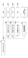
- the information processing apparatus 1 can take, for example, a configuration as shown in FIG. 2 as a configuration for supplying a clock.
- FIG. 2 is a configuration example for clock supply in the information processing apparatus 1 according to the first embodiment of the present invention.
- the information processing apparatus 1 includes, for example, a clock generator 70 that generates a reference clock having a frequency Fs, and phase offset units 72 # 2 to 72 # 4 for shifting the phases of clocks supplied to the cores 20 # 2 to 20 # 4. , And a frequency converter 80 that converts the reference clock of the frequency Fs into a frequency Fb that is four times as high as that to generate a bus clock.
- phase offset units 72 # 2 to 72 # 4 may delay the reference clock signal by having signal lines with different wiring lengths, or may include a buffer or the like.
- the clock generator 70 may generate a bus clock having the frequency Fb and convert it into a low-frequency reference clock having the frequency Fs by a frequency divider or the like.
- the clock generator 70 may generate clocks other than the frequencies Fb and Fs, and both the reference clock and the bus clock may be generated by frequency conversion.
- the device that generates the reference clock and the device that generates the bus clock may be separate.
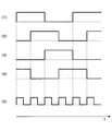
- FIG. 3 is a timing chart showing changes in the clock and bus clock supplied to each core in the information processing apparatus 1 according to the first embodiment of the present invention.
- (1) shows the change of the clock supplied to the core 20 # 1
- (2) shows the change of the clock supplied to the core 20 # 2
- (3) shows the core 20 #.
- 3 shows a change in the clock supplied to 3
- (4) shows a change in the clock supplied to the core 20 # 4.
- (5) shows the change of the bus clock.
- the cores 20 # 1 to 20 # 4 operate sequentially with a phase shift of 1 ⁇ 4 period with reference to the reference clock.
- a period corresponding to the phase difference coincides with one cycle of the bus clock.
- the problem that interference occurs when different cores simultaneously access the DRAM 50 can be solved.
- the core 20 # 1 executes a load instruction from the DRAM 50
- the execution result is stored in an internal register or the like of the core 20 # 1 before the rise of the clock supplied to the core 20 # 2. Therefore, even if the core 20 # 2 subsequently executes the memory access instruction, the memory access instruction does not interfere with the load instruction by the core 20 # 1.
- the number of cores and the ratio (Fb / Fs) of the frequency Fb of the bus clock to the frequency Fs of the reference clock are matched.
- the rising edge of the clock supplied to each core coincides with the rising edge of the bus clock. Until the rise of the clock supplied to the core).
- each core can execute a memory access instruction at the rising timing of the supplied clock.
- the rising edge of the reference clock and the rising edge of the bus clock do not necessarily coincide with each other, and the bus clock may be steadily delayed slightly in consideration of a communication delay or the like.
- the frequency ratio (Fb / Fs) is preferably equal to or larger than the number of cores accessing the DRAM 50” is as follows. Based on the desirability of assigning a bus clock of a period or more. When the DRAM controller 30 operates on both the rising and falling edges of the bus clock, the bus clock for two clocks is substantially allocated during the operation timing period of each core, and the execution of the memory access instruction Can be performed more reliably.
- the information processing apparatus 1 it is possible to reliably avoid memory access interference. Further, the memory access instruction can be surely executed during the operation timing period of each core. Furthermore, since the frequency of the clock supplied to the CPU core is relatively low, power consumption and heat generation due to the operation of the CPU can be suppressed, and costs can be reduced.
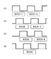
- FIG. 4 is a timing chart showing a state of task processing by a conventional single-core processor and a state in which the same task processing is executed by a conventional multi-core processor (4 cores).
- FIG. 4 shows that a conventional single-core processor is triggered by the rising edge of the supplied clock, and task 1-1 ⁇ task 2 ⁇ task 3 ⁇ task 4 ⁇ task 1-2 ⁇ task 1-3 ⁇ task 1 -4 shows a state in which processing is executed in the order of -4.
- a conventional single core processor requires 7 clocks for these processes.
- the task 1-1, the task 1-2, the task 1-3, and the task 1-4 are complete because there is an orderly task, that is, the processing result of the previous task is used in the subsequent task. This task cannot be executed in parallel.
- the second and lower stages in FIG. 4 show how the conventional multi-core processor performs distributed processing on the same task as the conventional single-core processor executes.
- (1) shows a clock supplied to the core # 1, and tasks executed by the core # 1 triggered by the rise of each clock
- the tasks executed by the core # 2 with each clock rising as a trigger are shown.
- (3) shows the clock supplied to the core # 3 and the task executed by the core # 3 with each clock rising as a trigger.
- (4) indicates a clock supplied to the core # 4 and a task executed by the core # 4 with the rise of each clock as a trigger.
- FIG. 5 is a diagram illustrating a state in which the information processing apparatus 1 according to the present embodiment executes the same task as the task illustrated in FIG.
- the information processing apparatus 1 of the present embodiment can execute the same task as the task requiring 4 clocks by the conventional multi-core processor shown in FIG. 4 in a few clocks. That is, the information processing apparatus 1 according to the present embodiment can realize a rapid parallel / distributed process.
- the information processing apparatus 1 of the present embodiment described above it is possible to reliably avoid memory access interference and suppress power consumption and heat generation.
- rapid parallel / distributed processing can be realized using a relatively low clock frequency.
- the information processing apparatus 2 is configured as a multicore processor as illustrated in FIG. 1, for example, but may be configured as an apparatus of another aspect such as a multiprocessor processing apparatus.
- the information processing apparatus 2 when the information processing apparatus 2 is mounted on a vehicle, the information processing apparatus 2 functions as an engine control apparatus that controls, for example, a multi-cylinder engine.
- each core takes charge of each cylinder, and executes a calculation for determining the ignition timing by an igniter attached to each cylinder.
- the information processing device 2 is not limited to this, and can function as a control device that controls various in-vehicle devices, but is particularly suitable for a device that repeatedly executes periodic processing, such as the engine control device described above. Applies to
- the frequency Fb of the bus clock supplied to the internal bus 40 and the data bus 60 is, for example, 800 [MHz].
- the frequency Fs of the reference clock serving as the operation reference for the cores 20 # 1 to 20 # 4 is, for example, 400 [MHz].
- the frequency Fb of the bus clock in this embodiment is twice the frequency Fs of the reference clock, and is matched with 1 ⁇ 2 of the number of cores.
- the frequency ratio (Fb / Fs) is equal to or larger than 1 ⁇ 2 of the number of cores accessing the DRAM 50.
- the frequency ratio (Fb / Fs) is preferably 1 or more, and if the number of cores accessing the DRAM 50 is eight, the frequency ratio. (Fb / Fs) is desirably 4 or more.
- the cores 20 # 1 to 20 # 4 operate sequentially with a phase shift of 1/8 period with the above-described reference clock as a reference.
- the core 20 # 1 operates according to the reference clock
- the core 20 # 1 operates with a delay of 1/8 cycle of the reference clock
- the core 20 # 3 with a delay of 1/4 cycle of the reference clock.
- the core 20 # 4 operates with a delay of 3/8 period of the reference clock.
- the core 20 # 1 operates with a delay of 1/2 cycle of the reference clock
- the core 20 # 1 operates with a delay of 5/8 cycle of the reference clock
- the core 20 # 3 operates with 3 /
- the core 20 # 4 operates with a delay of 4/8 cycles of the reference clock.
- Each core repeats the above (1) and (2) alternately.
- the reason why the cores 20 # 1 to 20 # 4 operate sequentially with a phase shift of 1/8 period is based on a value obtained by dividing 1 by twice (8) the number of cores (4).
- the frequency conversion unit 80 converts the reference clock having the frequency Fs to the doubled frequency Fb to generate a bus clock.
- FIG. 6 is a timing chart showing changes in the clock and bus clock supplied to each core in the information processing apparatus 2 according to the second embodiment of the present invention.
- (1) shows the change of the clock supplied to the core 20 # 1
- (2) shows the change of the clock supplied to the core 20 # 2
- (3) shows the core 20 #.
- 3 shows a change in the clock supplied to 3
- (4) shows a change in the clock supplied to the core 20 # 4.
- (5) shows the change of the bus clock.
- the cores 20 # 1 to 20 # 4 operate sequentially with a phase shift of 1 ⁇ 4 period with reference to the reference clock.
- a period corresponding to the phase difference coincides with a half cycle of the bus clock.
- the DRAM controller 30 operates at both rising and falling edges of the bus clock.
- a bus clock of substantially one clock is allocated during the operation timing period of each core.
- the problem that interference occurs when different cores simultaneously access the DRAM 50 can be solved.
- the core 20 # 1 executes a load instruction from the DRAM 50
- the execution result is stored in an internal register or the like of the core 20 # 1 before the rise of the clock supplied to the core 20 # 2. Therefore, even if the core 20 # 2 subsequently executes the memory access instruction, the memory access instruction does not interfere with the load instruction by the core 20 # 1.
- each core can execute a memory access instruction at the rise timing of the supplied clock.
- the ratio of the frequencies (Fb / Fs) is preferably equal to or larger than 1 ⁇ 2 of the number of cores accessing the DRAM 50” is the operation timing period of each core as described above. It is based on the need to allocate a bus clock of more than half a cycle.
- the information processing apparatus 2 it is possible to reliably avoid memory access interference. Further, the memory access instruction can be surely executed during the operation timing period of each core. Furthermore, since the frequency of the clock supplied to the CPU core is relatively low, power consumption and heat generation due to the operation of the CPU can be suppressed, and costs can be reduced. Compared with the first embodiment, it is possible to realize higher-speed processing when it is assumed that the bus clock frequency is the same.
- rapid parallel / distributed processing can be realized using a relatively low clock frequency.
- a clock whose phase is shifted from the reference clock is supplied to each core, but the same clock may be supplied to each core so that only the operation timing is shifted inside the core.
- Information processing device 10 Microcomputer 20 CPU 20 # 1, 20 # 2, 20 # 3, 20 # 4 Core 30 DRAM controller 40 Internal bus 50 DRAM 60 data bus 70 clock generator 72 # 2-72 # 4 phase offset unit 72 80 Frequency converter
Landscapes
- Engineering & Computer Science (AREA)
- Theoretical Computer Science (AREA)
- Physics & Mathematics (AREA)
- General Engineering & Computer Science (AREA)
- General Physics & Mathematics (AREA)
- Microcomputers (AREA)
Abstract
複数の命令実行手段と、該複数の命令実行手段によりアクセスされるメモリと、を備える情報処理装置であって、前記複数の命令実行手段は、基準クロックを基準として他の命令実行手段と位相差をもって動作し、前記複数の命令実行手段と前記メモリとを接続するバスに供給されるバスクロックの周波数は、前記基準クロックの周波数のn倍である(n≧2)ことを特徴とする、情報処理装置。
Description
本発明は、複数の命令実行手段を備える情報処理装置に関する。
近年、マルチプロセッサ処理装置やマルチコア・プロセッサのように、命令実行手段を複数個備える情報処理装置が普及している。
こうした命令実行手段を複数個備える情報処理装置では、異なる命令実行手段が同一のメモリを使用する場合、異なる命令実行手段が同一のメモリに同時にアクセスすることにより干渉が生じ、処理の遅延や混乱が発生しうるという課題がある。
特許文献1では、複数のプロセッサコアと複数のハードウエアアクセラレータがバスを介して接続された非対照マルチプロセッサについての発明が開示されている。この非対照マルチプロセッサは、プロセッサコアとハードウエアアクセラレータを含むグループを形成している。そして、この非対象マルチプロセッサは、各グループの入口部に、供給されるクロック信号を遅延して各グループ間のクロック位相を任意にずらすクロック遅延生成部を備えている。これによって、この非対象マルチプロセッサは、ピーク電流を抑制して誤作動の防止を図っている。
しかしながら、上記特許文献1に記載の非対照マルチプロセッサでは、異なる命令実行手段が同一のメモリに同時にアクセスすることにより干渉が生じるという課題を解決できない場合がある。各グループ間のクロック位相をずらしただけでは、当該ずらした位相に相当する期間内にメモリアクセス処理が終了しない場合があるからである。この結果、あるグループによるメモリアクセス処理が実行されている間に、他のグループによって同一のメモリにアクセスが開始される場合が生じ、前述のような干渉が生じてしまう可能性がある。
本発明はこのような課題を解決するためのものであり、メモリアクセスの干渉を確実に回避すると共に、電力消費や発熱を抑制することが可能な情報処理装置を提供することを、主たる目的とする。
上記目的を達成するための本発明の一態様は、
複数の命令実行手段と、
該複数の命令実行手段によりアクセスされるメモリと、
を備える情報処理装置であって、
前記複数の命令実行手段は、基準クロックを基準として他の命令実行手段と位相差をもって動作し、
前記複数の命令実行手段と前記メモリとを接続するバスに供給されるバスクロックの周波数は、前記基準クロックの周波数のn倍である(n≧2)ことを特徴とする、
情報処理装置である。
複数の命令実行手段と、
該複数の命令実行手段によりアクセスされるメモリと、
を備える情報処理装置であって、
前記複数の命令実行手段は、基準クロックを基準として他の命令実行手段と位相差をもって動作し、
前記複数の命令実行手段と前記メモリとを接続するバスに供給されるバスクロックの周波数は、前記基準クロックの周波数のn倍である(n≧2)ことを特徴とする、
情報処理装置である。
この本発明の一態様によれば、複数の命令実行手段は、基準クロックを基準として他の命令実行手段と位相差をもって動作し、複数の命令実行手段とメモリとを接続するバスに供給されるバスクロックの周波数は、基準クロックの周波数のn倍である(n≧2)ため、各命令実行手段の実行期間中にバスクロックの一周期以上が割り当てられ、メモリアクセスの干渉を確実に回避することができる。
また、命令実行手段が動作基準とする基準クロックの周波数を比較的低くすることができるため、電力消費や発熱を抑制することができる。
本発明によれば、メモリアクセスの干渉を確実に回避すると共に、電力消費や発熱を抑制することが可能な情報処理装置を提供することができる。
以下、本発明を実施するための形態について、添付図面を参照しながら実施例を挙げて説明する。
<第1実施例>
以下、図面を参照し、本発明の第1実施例に係る情報処理装置1について説明する。情報処理装置1は、例えば以下に例示するようなマルチコア・プロセッサとして構成されるが、マルチプロセッサ処理装置等、命令実行手段を複数個備える他の態様の装置として構成されてもよい。
以下、図面を参照し、本発明の第1実施例に係る情報処理装置1について説明する。情報処理装置1は、例えば以下に例示するようなマルチコア・プロセッサとして構成されるが、マルチプロセッサ処理装置等、命令実行手段を複数個備える他の態様の装置として構成されてもよい。
図1は、本発明の第1実施例に係る情報処理装置1の主要なシステム構成例である。情報処理装置1は、主要な構成として、マイコン10と、DRAM50と、を備える。
マイコン10の内部では、CPU20とDRAMコントローラ30が内部バス40で接続されている。CPU20は、プロセッサ・パッケージ内に複数のコア20#1~コア20#4を封入しており、これらのコアによって並行・独立して処理を実行可能となっている。
コア20#1~20#4は、命令デコーダ、レジスタ、演算回路、キャッシュメモリ等を有し、図示しないROMに格納されたプログラム(命令)を専用レジスタにフェッチし、これをデコードして実行することにより、種々の処理を行なうことができる。コア20#1~コア20#4の処理結果は、レジスタ等に格納される他、必要に応じてDRAM50に送出される。
ここで、情報処理装置1が車両に搭載される場合、情報処理装置1は、例えば多気筒エンジンの制御を行うエンジン制御装置として機能する。この場合、各コアは、各気筒をそれぞれ担当し、各気筒に取り付けられたイグナイターによる点火時期を決定するための演算を実行する。これに限らず、情報処理装置1は種々の車載機器を制御する制御装置として機能することが可能であるが、特に、上記のエンジン制御装置のように周期的な処理を繰り返し実行する装置に好適に適用される。
マイコン10とDRAM50は、データバス60で接続されている。DRAM50は、例えばDDR3-SDRAM(Double-Data-Rate3 Synchronous Dynamic Random Access Memory)の規格に準じたメモリである。
内部バス40及びデータバス60に供給されるバスクロックの周波数Fbは、例えば800[MHz]である。そして、コア20#1~コア20#4の動作基準となる基準クロックの周波数Fsは、例えば200[MHz]である。
本実施例におけるバスクロックの周波数Fbは、基準クロックの周波数Fsの4倍であり、コアの個数と合致させている。このように、周波数の比率(Fb/Fs)は、DRAM50にアクセスするコアの個数と同じか、それよりも大きいことが望ましい。例えば、DRAM50にアクセスするコアの個数が2個であれば、周波数の比率(Fb/Fs)は2以上であることが望ましく、DRAM50にアクセスするコアの個数が8個であれば、周波数の比率(Fb/Fs)は8以上であることが望ましい。
なお、200[MHz]や800[MHz]といった数値はあくまで一例であり、本発明はこれらの数値に何ら限定されるものではない。
一方、コア20#1~20#4は、前述の基準クロックを基準として、1/4周期ずつ位相をずらして順に動作する。例えば、コア20#1は基準クロック通りに動作し、コア20#1は基準クロックの1/4周期遅れで動作し、コア20#3は基準クロックの1/2周期遅れで動作し、コア20#4は基準クロックの3/4周期遅れで動作する。コア20#1~20#4が1/4周期ずつ位相をずらして順に動作するのは、コアの個数(4個)で1を除した値に基づいている。
情報処理装置1は、クロック供給のための構成として、例えば図2のような構成をとり得る。図2は、本発明の第1実施例に係る情報処理装置1におけるクロック供給のための構成例である。情報処理装置1は、例えば周波数Fsの基準クロックを発生させるクロックジェネレータ70と、コア20#2~コア20#4に供給するクロックの位相をずらすための位相オフセット部72#2~72#4と、周波数Fsの基準クロックを4倍の周波数Fbに変換してバスクロックを生成する周波数変換部80と、を備える。
位相オフセット回路の具体的態様については種々のものが知られている。位相オフセット部72#2~72#4は、例えば、配線長の異なる信号線を有することによって基準クロック信号を遅延させるものであってもよいし、バッファ等を備えるものであってもよい。
なお、上記の構成に換えて、クロックジェネレータ70が周波数Fbのバスクロックを生成し、これを分周器等によって周波数Fsの低周波な基準クロックに変換する構成であってもよい。また、クロックジェネレータ70が周波数Fb、Fs以外のクロックを生成し、基準クロックとバスクロックの双方が周波数変換によって生成されるものであってもよい。また、基準クロックを生成する機器とバスクロックを生成する機器は別体であっても構わない。
係る構成によって、以下のような動作が実現される。図3は、本発明の第1実施例に係る情報処理装置1における、各コアに供給されるクロック、及びバスクロックの変化を示すタイミングチャートである。図中、(1)はコア20#1に供給されるクロックの変化を示しており、(2)はコア20#2に供給されるクロックの変化を示しており、(3)はコア20#3に供給されるクロックの変化を示しており、(4)はコア20#4に供給されるクロックの変化を示している。また、図中、(5)はバスクロックの変化を示している。
図示するように、コア20#1~20#4は、基準クロックを基準として、1/4周期ずつ位相をずらして順に動作する。そして、その位相差に相当する期間は、バスクロックの一周期に一致している。
この結果、異なるコアがDRAM50に同時にアクセスすることにより干渉が生じるという課題を解決することができる。例えばコア20#1がDRAM50からのロード命令を実行した場合、その実行結果はコア20#2に供給されるクロックの立ち上がり前に、コア20#1の内部レジスタ等に格納されることになる。従って、続いてコア20#2がメモリアクセス命令を実行したとしても、当該メモリアクセス命令はコア20#1によるロード命令とは干渉しない。
また、本発明の第1実施例に係る情報処理装置1では、コアの個数と、バスクロックの周波数Fbと基準クロックの周波数Fsの比率(Fb/Fs)を一致させている。この結果、各コアに供給されるクロックの立ち上がりと、バスクロックの立ち上がりが一致することになり、バスクロックの一周期が必ず各コアの動作期間(自コアに供給されるクロックの立ち上がりから次のコアに供給されるクロックの立ち上がりまで)に割り当てられることになる。
従って、各コアは、供給されたクロックの立ち上がりのタイミングでメモリアクセス命令を実行することが可能となる。なお、基準クロックの立ち上がりとバスクロックの立ち上がりを必ずしも完全に一致させる必要はなく、通信遅延等を考慮してバスクロックを定常的に若干遅らせる等してもよい。
前述の、「周波数の比率(Fb/Fs)は、DRAM50にアクセスするコアの個数と同じか、それよりも大きいことが望ましい」なる記載は、このように各コアの動作タイミング期間中に、一周期以上のバスクロックを割り当てるこが望ましいことに基づく。なお、DRAMコントローラ30がバスクロックの立ち上がり及び立ち下がりの双方で動作する場合、各コアの動作タイミング期間中に、実質的に2クロック分のバスクロックが割り当てられることになり、メモリアクセス命令の実行をより確実に行うことができる。
この結果、本発明の第1実施例に係る情報処理装置1では、メモリアクセスの干渉を確実に回避することができる。また、各コアの動作タイミング期間中において、メモリアクセス命令を確実に実行することができる。更に、CPUコアに供給されるクロックの周波数を比較的低くするため、CPUの動作による電力消費や発熱を抑制し、コストを低減することもできる。
ここで、従来のマルチコア装置との比較について述べる。図4は、従来のシングルコア・プロセッサによるタスク処理の様子、及び従来のマルチコア・プロセッサ(4コア)により同じタスク処理が実行される様子を示したタイミングチャートである。
図4の上段は、従来のシングルコア・プロセッサが、供給されたクロックの立ち上がりをトリガーとして、タスク1-1→タスク2→タスク3→タスク4→タスク1-2→タスク1-3→タスク1-4の順に処理を実行する様子を示している。従来のシングルコア・プロセッサでは、これらの処理に7クロックを要している。ここで、タスク1-1、タスク1-2、タスク1-3、タスク1-4は、順序性の存在するタスク、すなわち先のタスクの処理結果を後のタスクで用いる等の理由により、完全に並行しては実行できないタスクである。
また、図4の二段目以下は、従来のマルチコア・プロセッサが、上記従来のシングルコア・プロセッサが実行するのと同一のタスクを分散処理する様子を示している。図中、(1)はコア#1に供給されるクロックと、各クロックの立ち上がりをトリガーとしてコア#1により実行されるタスクを示しており、(2)はコア#2に供給されるクロックと、各クロックの立ち上がりをトリガーとしてコア#2により実行されるタスクを示しており、(3)はコア#3に供給されるクロックと、各クロックの立ち上がりをトリガーとしてコア#3により実行されるタスクを示しており、(4)はコア#4に供給されるクロックと、各クロックの立ち上がりをトリガーとしてコア#4により実行されるタスクを示している。
上記のように、タスク1-1、タスク1-2、タスク1-3、タスク1-4には順序性が存在するため、従来のマルチコア・プロセッサでは、例えばコア#1のみにこれらを実行させる必要がある。この結果、処理の分散が不十分となり、図4の例では全ての処理を終了するのに4クロックを要することになる。
これに対し、[背景技術]において例示した特許文献1に記載の装置では、各グループ間のクロック位相をずらしているため、順序性の存在するタスクを並列することが可能とも考えられる。しかしながら、当該ずらした位相に相当する期間内にメモリアクセス処理が終了しない場合があり、メモリアクセス命令が干渉して処理の遅延や混乱が生じる可能性がある。
この点、本実施例の情報処理装置1では、バスクロックの一周期が必ず各コアの動作期間に割り当てられることになるため、メモリアクセス命令の干渉を回避しつつ分散処理を実現することができる。図5は、図4で例示したタスクと同一のタスクを本実施例の情報処理装置1が実行する様子を示す図である。図示するように、本実施例の情報処理装置1は、図4に示した従来のマルチコア・プロセッサが4クロックを要したタスクと同一のタスクを、2クロック少々で実行することができる。すなわち、本実施例の情報処理装置1は、迅速な並行・分散処理を実現することができる。
以上説明した本実施例の情報処理装置1によれば、メモリアクセスの干渉を確実に回避すると共に、電力消費や発熱を抑制することができる。
また、比較的低いクロック周波数を用いて、迅速な並行・分散処理を実現することができる。
更に、各コアに供給されるクロックの位相をずらすことにより、突入電流の増加を抑制することができ、電力消費やノイズを低減することができる。
<第2実施例>
以下、図面を参照し、本発明の第2実施例に係る情報処理装置2について説明する。情報処理装置2は、例えば図1に示したようなマルチコア・プロセッサとして構成されるが、マルチプロセッサ処理装置等、他の態様の装置として構成されてもよい。
以下、図面を参照し、本発明の第2実施例に係る情報処理装置2について説明する。情報処理装置2は、例えば図1に示したようなマルチコア・プロセッサとして構成されるが、マルチプロセッサ処理装置等、他の態様の装置として構成されてもよい。
本発明の第2実施例に係る情報処理装置2の主要なシステム構成例については、第1実施例と共通するため、図1を参照することとして詳細な説明を省略する。
第1実施例と同様、情報処理装置2が車両に搭載される場合、情報処理装置2は、例えば多気筒エンジンの制御を行うエンジン制御装置として機能する。この場合、各コアは、各気筒をそれぞれ担当し、各気筒に取り付けられたイグナイターによる点火時期を決定するための演算を実行する。これに限らず、情報処理装置2は種々の車載機器を制御する制御装置として機能することが可能であるが、特に、上記のエンジン制御装置のように周期的な処理を繰り返し実行する装置に好適に適用される。
本実施例において、内部バス40及びデータバス60に供給されるバスクロックの周波数Fbは、例えば800[MHz]である。そして、コア20#1~コア20#4の動作基準となる基準クロックの周波数Fsは、例えば400[MHz]である。
本実施例におけるバスクロックの周波数Fbは、基準クロックの周波数Fsの2倍であり、コアの個数の1/2と合致させている。このように、周波数の比率(Fb/Fs)は、DRAM50にアクセスするコアの個数の1/2と同じか、それよりも大きいことが望ましい。例えば、DRAM50にアクセスするコアの個数が2個であれば、周波数の比率(Fb/Fs)は1以上であることが望ましく、DRAM50にアクセスするコアの個数が8個であれば、周波数の比率(Fb/Fs)は4以上であることが望ましい。
なお、400[MHz]や800[MHz]といった数値はあくまで一例であり、本発明はこれらの数値に何ら限定されるものではない。
一方、コア20#1~20#4は、前述の基準クロックを基準として、1/8周期ずつ位相をずらして順に動作する。例えば、(1)まず、コア20#1は基準クロック通りに動作し、コア20#1は基準クロックの1/8周期遅れで動作し、コア20#3は基準クロックの1/4周期遅れで動作し、コア20#4は基準クロックの3/8周期遅れで動作する。次に、(2)コア20#1は基準クロックの1/2周期遅れで動作し、コア20#1は基準クロックの5/8周期遅れで動作し、コア20#3は基準クロックの3/4周期遅れで動作し、コア20#4は基準クロックの7/8周期遅れで動作する。各コアは、上記(1)、(2)を交互に繰り返す。コア20#1~20#4が1/8周期ずつ位相をずらして順に動作するのは、コアの個数(4個)の2倍(8)で1を除した値に基づいている。
情報処理装置2における、クロック供給のための構成は、第1実施例と同様でよいため、図2等を参照することとして詳細な説明を省略する。周波数変換部80は、周波数Fsの基準クロックを2倍の周波数Fbに変換してバスクロックを生成する。
係る構成によって、以下のような動作が実現される。図6は、本発明の第2実施例に係る情報処理装置2における、各コアに供給されるクロック、及びバスクロックの変化を示すタイミングチャートである。図中、(1)はコア20#1に供給されるクロックの変化を示しており、(2)はコア20#2に供給されるクロックの変化を示しており、(3)はコア20#3に供給されるクロックの変化を示しており、(4)はコア20#4に供給されるクロックの変化を示している。また、図中、(5)はバスクロックの変化を示している。
図示するように、コア20#1~20#4は、基準クロックを基準として、1/4周期ずつ位相をずらして順に動作する。そして、その位相差に相当する期間は、バスクロックの半周期に一致している。本実施例において、DRAMコントローラ30は、バスクロックの立ち上がり及び立ち下がりの双方で動作する。この結果、各コアの動作タイミング期間中に、実質的に1クロック分のバスクロックが割り当てられることになる。
従って、異なるコアがDRAM50に同時にアクセスすることにより干渉が生じるという課題を解決することができる。例えばコア20#1がDRAM50からのロード命令を実行した場合、その実行結果はコア20#2に供給されるクロックの立ち上がり前に、コア20#1の内部レジスタ等に格納されることになる。従って、続いてコア20#2がメモリアクセス命令を実行したとしても、当該メモリアクセス命令はコア20#1によるロード命令とは干渉しない。
また、本発明の第2実施例に係る情報処理装置2では、コアの個数の1/2と、バスクロックの周波数Fbと基準クロックの周波数Fsの比率(Fb/Fs)を一致させている。この結果、各コアに供給されるクロックの立ち上がりと、バスクロックの立ち上がり又は立ち下がりが一致することになり、バスクロックの半周期が必ず各コアの動作期間に割り当てられることになる。
本実施例におけるDRAMコントローラ30は、バスクロックの立ち上がり及び立ち下がりの双方で動作するため、各コアは、供給されたクロックの立ち上がりのタイミングでメモリアクセス命令を実行することが可能となる。
前述の、「周波数の比率(Fb/Fs)は、DRAM50にアクセスするコアの個数の1/2と同じか、それよりも大きいことが望ましい」なる記載は、このように各コアの動作タイミング期間中に、半周期以上のバスクロックを割り当てる必要があることに基づく。
この結果、本発明の第2実施例に係る情報処理装置2では、メモリアクセスの干渉を確実に回避することができる。また、各コアの動作タイミング期間中において、メモリアクセス命令を確実に実行することができる。更に、CPUコアに供給されるクロックの周波数を比較的低くするため、CPUの動作による電力消費や発熱を抑制し、コストを低減することもできる。なお、第1実施例と比較すると、バスクロックの周波数が同じであると仮定した場合に、より高速な処理を実現することが可能である。
図4及び図5によって説明した従来のマルチコア装置との比較については、第1実施例と同様であるため、説明を省略する。
以上説明した本実施例の情報処理装置2によれば、メモリアクセスの干渉を確実に回避すると共に、電力消費や発熱を抑制することができる。
また、比較的低いクロック周波数を用いて、迅速な並行・分散処理を実現することができる。
更に、各コアに供給されるクロックの位相をずらすことにより、突入電流の増加を抑制することができ、電力消費やノイズを低減することができる。
以上、本発明を実施するための最良の形態について実施例を用いて説明したが、本発明はこうした実施例に何等限定されるものではなく、本発明の要旨を逸脱しない範囲内において種々の変形及び置換を加えることができる。
例えば、基準クロックから位相のずれたクロックを各コアに供給するものとしたが、各コアに同一のクロックを供給し、コアの内部において動作タイミングのみをずらす構成でもよい。
1、2 情報処理装置
10 マイコン
20 CPU
20#1、20#2、20#3、20#4 コア
30 DRAMコントローラ
40 内部バス
50 DRAM
60 データバス
70 クロックジェネレータ
72#2~72#4 位相オフセット部72
80 周波数変換部
10 マイコン
20 CPU
20#1、20#2、20#3、20#4 コア
30 DRAMコントローラ
40 内部バス
50 DRAM
60 データバス
70 クロックジェネレータ
72#2~72#4 位相オフセット部72
80 周波数変換部
Claims (8)
- 複数の命令実行手段と、
該複数の命令実行手段によりアクセスされるメモリと、
を備える情報処理装置であって、
前記複数の命令実行手段は、基準クロックを基準として他の命令実行手段と位相差をもって動作し、
前記複数の命令実行手段と前記メモリとを接続するバスに供給されるバスクロックの周波数は、前記基準クロックの周波数のn倍である(n≧2)ことを特徴とする、
情報処理装置。 - 請求項1に記載の情報処理装置であって、
前記バスクロックの周期は、前記位相差に相当する期間と等しい、又は前記位相差に相当する期間に比して小さいことを特徴とする、情報処理装置。 - 請求項1に記載の情報処理装置であって、
前記nは、前記同一のメモリにアクセスする複数の命令実行手段の個数以上の値である、情報処理装置。 - 請求項3に記載の情報処理装置であって、
前記複数の命令実行手段は、前記基準クロックを基準として1/n周期ずつ位相をずらして順に動作することを特徴とする、情報処理装置。 - 複数の命令実行手段と、
該複数の命令実行手段によりアクセスされるメモリと、
を備える情報処理装置であって、
前記複数の命令実行手段は、基準クロックを基準として他の命令実行手段と位相差をもって動作し、
前記複数の命令実行手段と前記メモリとを接続するバスに供給されるバスクロックの周波数は、前記基準クロックの周波数のn倍であり(n≧1)、且つ、該バスクロックの1/2周期は、前記位相差に相当する期間と等しい、又は前記位相差に相当する期間に比して小さいことを特徴とする、
情報処理装置。 - 請求項5に記載の情報処理装置であって、
前記nは、前記同一のメモリにアクセスする複数の命令実行手段の個数の1/2以上の値である、情報処理装置。 - 請求項6に記載の情報処理装置であって、
前記複数の命令実行手段は、前記基準クロックを基準として1/n周期ずつ位相をずらして順に動作し、
前記複数の命令実行手段と前記メモリとを接続するバスを制御する制御手段は、バスクロックの立ち上がり及び立ち下がりの双方で動作することを特徴とする、情報処理装置。 - 車両に搭載され、車載機器の制御のための情報処理を実行する、請求項1ないし7のいずれか1項に記載の情報処理装置。
Priority Applications (1)
| Application Number | Priority Date | Filing Date | Title |
|---|---|---|---|
| PCT/JP2010/050641 WO2011089696A1 (ja) | 2010-01-20 | 2010-01-20 | 情報処理装置 |
Applications Claiming Priority (1)
| Application Number | Priority Date | Filing Date | Title |
|---|---|---|---|
| PCT/JP2010/050641 WO2011089696A1 (ja) | 2010-01-20 | 2010-01-20 | 情報処理装置 |
Publications (1)
| Publication Number | Publication Date |
|---|---|
| WO2011089696A1 true WO2011089696A1 (ja) | 2011-07-28 |
Family
ID=44306519
Family Applications (1)
| Application Number | Title | Priority Date | Filing Date |
|---|---|---|---|
| PCT/JP2010/050641 Ceased WO2011089696A1 (ja) | 2010-01-20 | 2010-01-20 | 情報処理装置 |
Country Status (1)
| Country | Link |
|---|---|
| WO (1) | WO2011089696A1 (ja) |
Citations (3)
| Publication number | Priority date | Publication date | Assignee | Title |
|---|---|---|---|---|
| JPS58149555A (ja) * | 1982-02-27 | 1983-09-05 | Fujitsu Ltd | 並列処理装置 |
| JPS61121172A (ja) * | 1984-11-19 | 1986-06-09 | Fujitsu Ltd | 位相分割処理方式 |
| JPH05101207A (ja) * | 1991-10-09 | 1993-04-23 | Matsushita Electric Ind Co Ltd | Simd型プロセツサ |
-
2010
- 2010-01-20 WO PCT/JP2010/050641 patent/WO2011089696A1/ja not_active Ceased
Patent Citations (3)
| Publication number | Priority date | Publication date | Assignee | Title |
|---|---|---|---|---|
| JPS58149555A (ja) * | 1982-02-27 | 1983-09-05 | Fujitsu Ltd | 並列処理装置 |
| JPS61121172A (ja) * | 1984-11-19 | 1986-06-09 | Fujitsu Ltd | 位相分割処理方式 |
| JPH05101207A (ja) * | 1991-10-09 | 1993-04-23 | Matsushita Electric Ind Co Ltd | Simd型プロセツサ |
Similar Documents
| Publication | Publication Date | Title |
|---|---|---|
| US7814252B2 (en) | Asymmetric multiprocessor | |
| JP6321807B2 (ja) | 車両のための制御装置 | |
| US20070255929A1 (en) | Multiprocessor System and Multigrain Parallelizing Compiler | |
| KR101380364B1 (ko) | 적어도 하나의 dma 주변장치 및 직각위상 클록으로 동작하는 cpu 사이의 싱글 포트 sram의 대역폭 공유 | |
| JP2013097659A (ja) | 半導体データ処理装置、タイムトリガ通信システム及び通信システム | |
| JP2010165247A (ja) | 半導体装置及びデータプロセッサ | |
| US9009513B2 (en) | Multiprocessor for providing timers associated with each of processor cores to determine the necessity to change operating frequency and voltage for per core upon the expiration of corresponding timer | |
| JP2010277180A (ja) | 情報処理システム及びデータ転送方法 | |
| US8261121B2 (en) | Command latency reduction and command bandwidth maintenance in a memory circuit | |
| JP2014191655A (ja) | マルチプロセッサ、電子制御装置、プログラム | |
| JP2011170619A (ja) | マルチスレッド処理装置 | |
| WO2011089696A1 (ja) | 情報処理装置 | |
| JP2015530644A (ja) | 遅延ロック・ループを使用するメモリ・デバイスのための省電力の装置及び方法 | |
| CN102253708B (zh) | 一种微处理器硬件多线程动态变频控制装置及其应用方法 | |
| US8970410B2 (en) | Semiconductor integrated circuit device and data processing system | |
| JP2004310394A (ja) | Sdramアクセス制御装置 | |
| CN103210377B (zh) | 信息处理系统 | |
| JP2010196619A (ja) | 内燃機関の制御装置 | |
| JP2010176403A (ja) | マルチスレッドプロセッサ装置 | |
| JP2008041106A (ja) | 半導体集積回路装置、クロック制御方法及びデータ転送制御方法 | |
| JP2008262340A (ja) | デュアルコア向け自動コード生成装置 | |
| US20070233934A1 (en) | Signal processor | |
| JP2007188171A (ja) | メモリコントローラ | |
| TWI816032B (zh) | 多核心處理器電路 | |
| CN113568665B (zh) | 一种数据处理装置 |
Legal Events
| Date | Code | Title | Description |
|---|---|---|---|
| 121 | Ep: the epo has been informed by wipo that ep was designated in this application |
Ref document number: 10843862 Country of ref document: EP Kind code of ref document: A1 |
|
| NENP | Non-entry into the national phase |
Ref country code: DE |
|
| 122 | Ep: pct application non-entry in european phase |
Ref document number: 10843862 Country of ref document: EP Kind code of ref document: A1 |
|
| NENP | Non-entry into the national phase |
Ref country code: JP |