WO2011065279A1 - Range sensor and range image sensor - Google Patents
Range sensor and range image sensor Download PDFInfo
- Publication number
- WO2011065279A1 WO2011065279A1 PCT/JP2010/070564 JP2010070564W WO2011065279A1 WO 2011065279 A1 WO2011065279 A1 WO 2011065279A1 JP 2010070564 W JP2010070564 W JP 2010070564W WO 2011065279 A1 WO2011065279 A1 WO 2011065279A1
- Authority
- WO
- WIPO (PCT)
- Prior art keywords
- semiconductor
- distance
- region
- image sensor
- semiconductor regions
- Prior art date
Links
- 239000004065 semiconductor Substances 0.000 claims abstract description 199
- 239000000758 substrate Substances 0.000 claims abstract description 57
- 238000001514 detection method Methods 0.000 description 43
- 238000009826 distribution Methods 0.000 description 13
- 238000010586 diagram Methods 0.000 description 11
- 238000003892 spreading Methods 0.000 description 11
- 230000007480 spreading Effects 0.000 description 11
- 239000012535 impurity Substances 0.000 description 9
- 238000012986 modification Methods 0.000 description 6
- 230000004048 modification Effects 0.000 description 6
- 238000004364 calculation method Methods 0.000 description 5
- 238000005259 measurement Methods 0.000 description 5
- 238000000034 method Methods 0.000 description 5
- 238000012546 transfer Methods 0.000 description 5
- 238000009825 accumulation Methods 0.000 description 4
- 230000006870 function Effects 0.000 description 4
- 238000003384 imaging method Methods 0.000 description 4
- 230000003287 optical effect Effects 0.000 description 4
- 230000004888 barrier function Effects 0.000 description 3
- 230000001788 irregular Effects 0.000 description 3
- 238000004519 manufacturing process Methods 0.000 description 3
- 239000000463 material Substances 0.000 description 3
- 230000004044 response Effects 0.000 description 3
- 238000002366 time-of-flight method Methods 0.000 description 3
- 229910004298 SiO 2 Inorganic materials 0.000 description 2
- 239000000969 carrier Substances 0.000 description 2
- 239000004020 conductor Substances 0.000 description 2
- 238000009792 diffusion process Methods 0.000 description 2
- 229910021420 polycrystalline silicon Inorganic materials 0.000 description 2
- 229920005591 polysilicon Polymers 0.000 description 2
- 230000035945 sensitivity Effects 0.000 description 2
- 238000003860 storage Methods 0.000 description 2
- 239000000853 adhesive Substances 0.000 description 1
- 230000001070 adhesive effect Effects 0.000 description 1
- 238000012937 correction Methods 0.000 description 1
- 230000003111 delayed effect Effects 0.000 description 1
- 238000011161 development Methods 0.000 description 1
- 239000000945 filler Substances 0.000 description 1
- 230000001678 irradiating effect Effects 0.000 description 1
- 230000002093 peripheral effect Effects 0.000 description 1
- 238000005036 potential barrier Methods 0.000 description 1
- 230000003014 reinforcing effect Effects 0.000 description 1
- 239000000523 sample Substances 0.000 description 1
- 230000003595 spectral effect Effects 0.000 description 1
- 230000001360 synchronised effect Effects 0.000 description 1
Images


Classifications
-
- G—PHYSICS
- G01—MEASURING; TESTING
- G01S—RADIO DIRECTION-FINDING; RADIO NAVIGATION; DETERMINING DISTANCE OR VELOCITY BY USE OF RADIO WAVES; LOCATING OR PRESENCE-DETECTING BY USE OF THE REFLECTION OR RERADIATION OF RADIO WAVES; ANALOGOUS ARRANGEMENTS USING OTHER WAVES
- G01S17/00—Systems using the reflection or reradiation of electromagnetic waves other than radio waves, e.g. lidar systems
- G01S17/02—Systems using the reflection of electromagnetic waves other than radio waves
- G01S17/06—Systems determining position data of a target
- G01S17/08—Systems determining position data of a target for measuring distance only
- G01S17/10—Systems determining position data of a target for measuring distance only using transmission of interrupted, pulse-modulated waves
-
- H—ELECTRICITY
- H01—ELECTRIC ELEMENTS
- H01L—SEMICONDUCTOR DEVICES NOT COVERED BY CLASS H10
- H01L27/00—Devices consisting of a plurality of semiconductor or other solid-state components formed in or on a common substrate
- H01L27/14—Devices consisting of a plurality of semiconductor or other solid-state components formed in or on a common substrate including semiconductor components sensitive to infrared radiation, light, electromagnetic radiation of shorter wavelength or corpuscular radiation and specially adapted either for the conversion of the energy of such radiation into electrical energy or for the control of electrical energy by such radiation
- H01L27/144—Devices controlled by radiation
- H01L27/146—Imager structures
- H01L27/14643—Photodiode arrays; MOS imagers
-
- G—PHYSICS
- G01—MEASURING; TESTING
- G01S—RADIO DIRECTION-FINDING; RADIO NAVIGATION; DETERMINING DISTANCE OR VELOCITY BY USE OF RADIO WAVES; LOCATING OR PRESENCE-DETECTING BY USE OF THE REFLECTION OR RERADIATION OF RADIO WAVES; ANALOGOUS ARRANGEMENTS USING OTHER WAVES
- G01S17/00—Systems using the reflection or reradiation of electromagnetic waves other than radio waves, e.g. lidar systems
- G01S17/88—Lidar systems specially adapted for specific applications
- G01S17/89—Lidar systems specially adapted for specific applications for mapping or imaging
-
- G—PHYSICS
- G01—MEASURING; TESTING
- G01S—RADIO DIRECTION-FINDING; RADIO NAVIGATION; DETERMINING DISTANCE OR VELOCITY BY USE OF RADIO WAVES; LOCATING OR PRESENCE-DETECTING BY USE OF THE REFLECTION OR RERADIATION OF RADIO WAVES; ANALOGOUS ARRANGEMENTS USING OTHER WAVES
- G01S7/00—Details of systems according to groups G01S13/00, G01S15/00, G01S17/00
- G01S7/48—Details of systems according to groups G01S13/00, G01S15/00, G01S17/00 of systems according to group G01S17/00
- G01S7/481—Constructional features, e.g. arrangements of optical elements
- G01S7/4814—Constructional features, e.g. arrangements of optical elements of transmitters alone
-
- G—PHYSICS
- G01—MEASURING; TESTING
- G01S—RADIO DIRECTION-FINDING; RADIO NAVIGATION; DETERMINING DISTANCE OR VELOCITY BY USE OF RADIO WAVES; LOCATING OR PRESENCE-DETECTING BY USE OF THE REFLECTION OR RERADIATION OF RADIO WAVES; ANALOGOUS ARRANGEMENTS USING OTHER WAVES
- G01S7/00—Details of systems according to groups G01S13/00, G01S15/00, G01S17/00
- G01S7/48—Details of systems according to groups G01S13/00, G01S15/00, G01S17/00 of systems according to group G01S17/00
- G01S7/481—Constructional features, e.g. arrangements of optical elements
- G01S7/4816—Constructional features, e.g. arrangements of optical elements of receivers alone
-
- G—PHYSICS
- G01—MEASURING; TESTING
- G01S—RADIO DIRECTION-FINDING; RADIO NAVIGATION; DETERMINING DISTANCE OR VELOCITY BY USE OF RADIO WAVES; LOCATING OR PRESENCE-DETECTING BY USE OF THE REFLECTION OR RERADIATION OF RADIO WAVES; ANALOGOUS ARRANGEMENTS USING OTHER WAVES
- G01S7/00—Details of systems according to groups G01S13/00, G01S15/00, G01S17/00
- G01S7/48—Details of systems according to groups G01S13/00, G01S15/00, G01S17/00 of systems according to group G01S17/00
- G01S7/483—Details of pulse systems
- G01S7/486—Receivers
- G01S7/4861—Circuits for detection, sampling, integration or read-out
- G01S7/4863—Detector arrays, e.g. charge-transfer gates
-
- H—ELECTRICITY
- H01—ELECTRIC ELEMENTS
- H01L—SEMICONDUCTOR DEVICES NOT COVERED BY CLASS H10
- H01L27/00—Devices consisting of a plurality of semiconductor or other solid-state components formed in or on a common substrate
- H01L27/14—Devices consisting of a plurality of semiconductor or other solid-state components formed in or on a common substrate including semiconductor components sensitive to infrared radiation, light, electromagnetic radiation of shorter wavelength or corpuscular radiation and specially adapted either for the conversion of the energy of such radiation into electrical energy or for the control of electrical energy by such radiation
- H01L27/144—Devices controlled by radiation
- H01L27/146—Imager structures
- H01L27/14601—Structural or functional details thereof
- H01L27/14603—Special geometry or disposition of pixel-elements, address-lines or gate-electrodes
-
- H—ELECTRICITY
- H01—ELECTRIC ELEMENTS
- H01L—SEMICONDUCTOR DEVICES NOT COVERED BY CLASS H10
- H01L27/00—Devices consisting of a plurality of semiconductor or other solid-state components formed in or on a common substrate
- H01L27/14—Devices consisting of a plurality of semiconductor or other solid-state components formed in or on a common substrate including semiconductor components sensitive to infrared radiation, light, electromagnetic radiation of shorter wavelength or corpuscular radiation and specially adapted either for the conversion of the energy of such radiation into electrical energy or for the control of electrical energy by such radiation
- H01L27/144—Devices controlled by radiation
- H01L27/146—Imager structures
- H01L27/14601—Structural or functional details thereof
- H01L27/1464—Back illuminated imager structures
Definitions
- the present invention relates to a distance sensor and a distance image sensor.
- a conventional active optical distance measuring sensor irradiates light from a light source for light projection such as an LED (Light Emitting Diode), and detects light reflected from the object with a light detection element. It is known to output a signal corresponding to the distance up to.
- the PSD Position Sensitive Detector
- the PSD is known as an optical triangulation type optical distance measuring sensor that can easily measure the distance to an object.
- TOF Time-Of-Flight
- Image sensors that can acquire distance information and image information at the same time on the same chip are required for in-vehicle use and factory automatic manufacturing systems. If an image sensor is installed in front of the vehicle, it is expected to be used for detection / recognition of the vehicle ahead and detection / recognition of pedestrians. Apart from image information, an image sensor that acquires a distance image composed of a single distance information or a plurality of distance information is also expected. It is preferable to use the TOF method for such a distance measuring sensor.
- the TOF method emits pulsed light from a light source for projection toward an object, and detects the pulsed light reflected by the object with a light detection element, thereby making the time difference between the emission timing of the pulsed light and the detection timing. Is measuring.
- the time difference ( ⁇ t) can be rephrased as the phase difference between the emission pulse from the light source and the detection pulse. If this phase difference is detected, the distance d to the object can be obtained.
- the charge distribution type image sensor has attracted attention as a light detection element for performing distance measurement by the TOF method. That is, in the charge distribution type image sensor, for example, the charge generated in the image sensor in response to the incident detection pulse is distributed in one potential well during the ON period of the outgoing pulse, and the other during the OFF period. Allocate to potential wells. In this case, the ratio of the amount of charge distributed to the left and right is proportional to the phase difference between the detection pulse and the emission pulse, that is, the time required for the pulsed light to fly at the speed of light over twice the distance to the object. .
- Various charge distribution methods are conceivable.
- Patent Document 1 as a distance sensor (distance image sensor) of a charge distribution method, a semiconductor substrate, a photogate electrode that is provided on the surface of the semiconductor substrate and has two sides whose planar shapes face each other, and the surface And a plurality of gate electrodes respectively provided adjacent to two sides of the photogate electrode, and a charge having a conductivity type different from that of the semiconductor substrate and flowing from a region immediately below the photogate electrode to a region immediately below each gate electrode And a plurality of semiconductor regions for reading out each of them.
- a distance sensor distance image sensor
- a bias voltage for example, 5 V
- the depletion layer extends not only from the region directly under the photogate electrode but also from each semiconductor region. If the depletion layer extends from each semiconductor region, the generated charge may be directly taken into the depletion layer spreading from each semiconductor region without being taken into the depletion layer spreading from the region immediately below the photogate electrode. .
- a signal based on the charge that reaches directly below the photogate electrode and is distributed by the gate electrode contributes to the distance information. For this reason, the charge directly taken into the depletion layer extending from each semiconductor region and accumulated in each semiconductor region becomes an unnecessary noise component (DC component).
- a distance sensor is provided with a light incident surface, a semiconductor substrate having a surface opposite to the light incident surface, a photogate electrode provided on the surface, and a photogate electrode on the surface adjacent to the photogate electrode. From the first and second gate electrodes, the first and second semiconductor regions for reading out the electric charge flowing from the region immediately below the photogate electrode and immediately below the first and second gate electrodes, and the first and second semiconductor regions, respectively A third semiconductor region that is provided apart from the light incident surface and has a conductivity type opposite to that of the first and second semiconductor regions.
- the third semiconductor region having a conductivity type opposite to that of the first and second semiconductor regions is provided away from the first and second semiconductor regions on the light incident surface side. For this reason, the depletion layer extending from the first and second semiconductor regions is prevented from spreading to the light incident surface side by the third semiconductor region, and extends beyond the third semiconductor region to the light incident surface side. Absent. As a result, it is possible to suppress the generated charge from being directly taken into the depletion layer spreading from the first and second semiconductor regions, and to suppress generation of unnecessary noise components.
- the depletion layer extending from the region immediately below the photogate electrode is not suppressed by the third semiconductor region and extends toward the light incident surface. Therefore, the third semiconductor region does not hinder the charge intake into the depletion layer extending from the region immediately below the photogate electrode.
- the third semiconductor region is provided apart from the first and second semiconductor regions, there is a barrier to the potential gradient from the region immediately below the photogate electrode toward the region immediately below the first and second semiconductor regions. It is not formed, and there is no trouble in charge transfer.
- the distance image sensor according to the present invention includes an imaging region composed of a plurality of units arranged one-dimensionally or two-dimensionally on a semiconductor substrate, and based on the amount of charge output from the unit, a distance image is obtained.
- the generated charge is suppressed from being directly taken into the depletion layer spreading from the first and second semiconductor regions, and generation of unnecessary noise components can be suppressed.
- the first and second gate electrodes may be provided around the first and second semiconductor regions so as to surround the first and second semiconductor regions.
- the first and second gate electrodes are positioned around the first and second semiconductor regions.
- the first and second semiconductor regions are also positioned around the first and second gate electrodes. Since the first and second gate electrodes surround the first and second semiconductor regions, by supplying a signal for transferring charges to the first and second gate electrodes, the charges from all directions are changed to the first and second gate electrodes. It is possible to transfer to the second semiconductor region. That is, substantially all the peripheral regions of the first and second gate electrodes can function as a charge generation region, and the aperture ratio is further improved significantly.
- the signal amount can be increased and a distance image with a good S / N ratio can be obtained.
- a distance image with a good S / N ratio can be obtained.
- the shape of the first and second gate electrodes may be annular. In this case, it is possible to steadily collect charges flowing into the regions immediately below the first and second gate electrodes from all directions, and to prevent the inflow thereof.
- the present invention it is possible to provide a distance sensor and a distance image sensor capable of suppressing the generation of unnecessary noise components and performing highly accurate distance detection.
- FIG. 5 is a diagram showing a cross-sectional configuration along the line VV in FIG. 4. It is a figure which shows potential distribution for demonstrating the accumulation
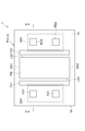
- FIG. 1 is an explanatory diagram showing the configuration of the distance measuring apparatus.
- the distance measuring device a distance image sensor 1, a light source 3 for emitting near-infrared light, a driving circuit 4 for giving a pulse drive signal S P to the light source 3, and a control circuit 2, the arithmetic circuit 5, the ing.
- the control circuit 2 includes first and second gate electrode included in each pixel of the range image sensor 1 (TX1, TX2: see FIG. 4), the pulsed driving signal S gate signal detection is synchronous with the P S 1, S 2 give.
- the arithmetic circuit 5 uses a signal d ′ (m, n) indicating distance information read from the first to fourth semiconductor regions (FD1 to FD4: see FIG. 4) of the distance image sensor 1 as an object such as a pedestrian.
- the distance to the object H is calculated.
- the distance in the horizontal direction D from the distance image sensor 1 to the object H is defined as d.
- the control circuit 2 is input to the pulse drive signal S P to the switch 4b of the driving circuit 4.
- a light projecting light source 3 comprising an LED or a laser diode is connected to a power source 4a via a switch 4b. Therefore, when the pulse drive signal S P is input to the switch 4b, a drive current having the same waveform as the pulse drive signal S P is supplied to the light source 3, the pulse light L P as a probe light for distance measurement from the light source 3 Is output.
- the pulse detection signal S D is outputted.
- the distance image sensor 1 is fixed on the wiring board 10. In the distance image sensor 1, a signal d ′ (m, n) having distance information is output from each pixel via a wiring on the wiring substrate 10.
- Pulse drive signal S P a square wave of period T, the high level "1", when the low level is "0", the voltage V (t) is given by the following equation.
- V (t) 0 (provided that (T / 2) ⁇ t ⁇ T)
- V (t + T) V (t)
- the waveforms of the detection gate signals S 1 and S 2 are square waves having a period T, and the voltage V (t) is given by the following equation.
- V (t) 0 (provided that (T / 2) ⁇ t ⁇ T)
- V (t + T) V (t)
- V (t) 0 (provided that 0 ⁇ t ⁇ (T / 2))
- V (t) 1 (provided that (T / 2) ⁇ t ⁇ T)
- V (t + T) V (t)
- the pulse signal S P, S 1, S 2 , S D has all pulse period 2 ⁇ T P.
- Detection gate signal S 1 and the pulse detection signal S D are both the amount of charge generated by the distance image sensor within 1 when "1" Q1, the detection gate signal S 2 and the pulse detection signal S D are both "1" In this case, the amount of charge generated in the distance image sensor 1 is Q2.
- the phase difference between one detection gate signal S 1 and the pulse detection signal SD in the distance image sensor 1 is the distance in the overlap period when the other detection gate signal S 2 and the pulse detection signal SD are “1”. It is proportional to the amount of charge Q2 generated in the image sensor 1. That is, the charge amount Q2 is the charge amount for the period logical product of the detection gate signal S 2 and the pulse detection signal S D is "1".
- the pulse detection signal SD is delayed.
- the arithmetic circuit 5 can calculate the distance d.
- the above-described pulse is repeatedly emitted, and the integrated value can be output as the respective charge amounts Q1 and Q2.
- the ratio of the charge amounts Q1 and Q2 to the total charge amount corresponds to the above-described phase difference, that is, the distance to the object H.
- the arithmetic circuit 5 calculates the distance to the object H according to this phase difference.
- a coefficient ⁇ for correcting the latter is obtained in advance, and the product after shipping is obtained by multiplying the calculated distance d by the coefficient ⁇ .
- the calculation distance d may be used.
- the distance calculation can be performed after performing the calculation for correcting the light speed c.
- the relationship between the signal input to the arithmetic circuit and the actual distance may be stored in advance in the memory, and the distance may be calculated by a lookup table method.
- the calculation method can also be changed depending on the sensor structure, and a conventionally known calculation method can be used for this.
- FIG. 2 is a diagram for explaining a cross-sectional configuration of the distance image sensor.
- the distance image sensor 1 includes a semiconductor substrate 1A.
- the semiconductor substrate 1A has a reinforcing frame portion F and a thin plate portion TF thinner than the frame portion F, and these are integrated.
- the thickness of the thin plate portion TF is 5 ⁇ m or more and 100 ⁇ m or less.
- the thickness of the frame portion F in this example is 200 ⁇ m or more and 600 ⁇ m or less.
- the entire semiconductor substrate 1A may be thinned.
- the range image sensor 1 a pulse light L D is made incident from the light incident surface 1BK.
- a surface 1FT opposite to the light incident surface 1BK of the distance image sensor 1 is connected to the wiring substrate 10 via an adhesion region AD.
- the adhesion region AD is a region including an adhesion element such as a bump electrode, and has an insulating adhesive or filler as necessary.
- FIG. 3 is a schematic plan view of the distance image sensor.
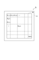
- the semiconductor substrate 1 ⁇ / b> A has an imaging region 1 ⁇ / b> B composed of a plurality of pixels P (m, n) arranged two-dimensionally. From each pixel P (m, n), two charge amounts (Q1, Q2) are output as the signal d '(m, n) having the above-described distance information. Each pixel P (m, n) outputs a signal d '(m, n) corresponding to the distance to the object H as a minute distance measuring sensor. Therefore, if the reflected light from the object H is imaged on the imaging region 1B, a distance image of the object as a collection of distance information to each point on the object H can be obtained.
- One pixel P (m, n) functions as one distance sensor.
- FIG. 4 is a schematic diagram for explaining the configuration of the pixels of the distance image sensor.
- FIG. 5 is a diagram showing a cross-sectional configuration along the line VV in FIG. In FIG. 4, the conductor 11 is not shown.
- the distance image sensor 1 includes a light incident surface 1BK and a semiconductor substrate 1A having a surface 1FT opposite to the light incident surface 1BK, a photogate electrode PG, first and second gate electrodes TX1 and TX2, Second semiconductor regions FD1 and FD2 and a third semiconductor region SR1 are provided.
- the photogate electrode PG is provided on the surface 1FT via the insulating layer 1E.
- the first and second gate electrodes TX1, TX2 are provided adjacent to the photogate electrode PG via the insulating layer 1E on the surface 1FT.
- the first and second semiconductor regions FD1 and FD2 accumulate charges that flow into regions immediately below the gate electrodes TX1 and TX2.
- the third semiconductor region SR1 is provided away from the first and second semiconductor regions FD1, FD2 toward the light incident surface 1BK, and has a conductivity type opposite to that of the first and second semiconductor regions FD1, FD2.
- the semiconductor substrate 1A of this example is S
- the insulating layer 1E is made of SiO 2 .
- the semiconductor substrate 1A may be made of an epitaxial layer.
- the photogate electrode PG has a rectangular shape in plan view.
- the photogate electrode PG has a rectangular shape. That is, the photogate electrode PG has a planar shape having first and second long sides LS1, LS2 facing each other and first and second short sides SS1, SS2 facing each other.
- a region corresponding to the photogate electrode PG in the semiconductor substrate 1A (a region immediately below the photogate electrode PG) functions as a photosensitive region in which charges are generated according to incident light.
- the photogate electrode PG is made of polysilicon, but other materials may be used.
- the first semiconductor region FD1 is disposed along the first long side LS1 on the first long side LS1 side of the photogate electrode PG.
- the second semiconductor region FD2 is disposed along the second long side LS2 on the second long side LS2 side of the photogate electrode PG.
- the first semiconductor region FD1 and the second semiconductor region FD2 are opposed to the first and second long sides LS1 and LS2 (hereinafter sometimes simply referred to as “opposing directions”) with the photogate electrode PG interposed therebetween. Opposite.
- the first and second semiconductor regions FD1, FD2 have a rectangular shape in plan view. In the present embodiment, the first and second semiconductor regions FD1, FD2 have a rectangular shape in which the long side direction of the photogate electrode PG is the long side direction.
- the first gate electrode TX1 is provided between the photogate electrode PG and the first semiconductor region FD1.
- the second gate electrode TX2 is provided between the photogate electrode PG and the second semiconductor region FD2.
- the first and second gate electrodes TX1, TX2 have a rectangular shape in plan view.
- the first and second gate electrodes TX1, TX2 have a rectangular shape in which the long side direction of the photogate electrode PG is the long side direction.
- the lengths of the first and second gate electrodes TX1, TX2 in the long side direction are set to be the same.
- the first and second gate electrodes TX1 and TX2 are made of polysilicon, but other materials may be used.
- the third semiconductor region SR1 is located between the first and second semiconductor regions FD1, FD2 and the light incident surface 1BK, and viewed from the direction orthogonal to the light incident surface 1BK, the first and second semiconductor regions FD1, It is formed so as to cover FD2.
- the third semiconductor region SR1 has a rectangular shape in plan view. In the present embodiment, the third semiconductor region SR1 has a rectangular shape in which the long side direction of the photogate electrode PG is the long side direction.
- the semiconductor substrate 1A is made of a low impurity concentration P-type semiconductor substrate, and the first and second semiconductor regions FD1 and FD2 are regions made of a high impurity concentration N-type semiconductor and are floating diffusion regions.
- the third semiconductor region SR1 is a region having the same conductivity type as the semiconductor substrate 1A and having a higher impurity concentration than the semiconductor substrate 1A, that is, a high impurity concentration P-type semiconductor.
- the third semiconductor region SR1 may be a P-type diffusion region or a P-type well region.
- each semiconductor region is as follows.
- Semiconductor substrate 1A thickness 5 to 100 ⁇ m / impurity concentration 1 ⁇ 10 12 to 10 15 cm ⁇ 3
- First and second semiconductor regions FD1, FD2 thickness 0.1 to 0.4 ⁇ m / impurity concentration 1 ⁇ 10 18 to 10 20 cm ⁇ 3
- Third semiconductor region SR1 thickness 0.5 to 5 ⁇ m / impurity concentration 1 ⁇ 10 15 to 10 19 cm ⁇ 3
- the insulating layer 1E is provided with contact holes for exposing the surfaces of the first and second semiconductor regions FD1, FD2.
- a conductor 11 for connecting the first and second semiconductor regions FD1, FD2 to the outside is disposed in the contact hole.
- Part of the first and second semiconductor regions FD1, FD2 is in contact with a region immediately below the gate electrodes TX1, TX2 in the semiconductor substrate 1A.
- An antireflection film 1D is provided on the light incident surface 1BK side of the semiconductor substrate 1A.
- the material of the antireflection film 1D is SiO 2 or SiN.
- the wiring substrate 10 is electrically connected to the first and second semiconductor regions FD1 and FD2, the first and second gate electrodes TX1 and TX2, the photogate electrode PG, and the like through bump electrodes in the adhesion region AD.
- a through electrode (not shown) is provided.
- the through electrode of the wiring board 10 is exposed on the back surface of the wiring board 10.
- a light shielding layer (not shown) is formed on the surface of the insulating substrate constituting the wiring substrate 10 on the interface side with the adhesion region AD. The light shielding layer suppresses incidence of light transmitted through the distance image sensor 1 to the wiring board 10. In this distance measuring device, when the distance image sensor 1 is mounted on the wiring board 10, the signal can be given to each electrode through each wiring, and the device is miniaturized.
- n-type semiconductor includes a positively ionized donor, has a positive potential, and attracts electrons.
- Pulse light L D from the object incident from the light incident surface (back surface) 1BK of the semiconductor substrate 1A leads to the region immediately below the photogate electrode PG provided on the surface side of the semiconductor substrate 1A.
- the charges generated in the semiconductor substrate 1A with the incidence of the pulsed light are distributed from the region immediately below the photogate electrode PG to the region immediately below the first and second gate electrodes TX1 and TX2 adjacent thereto.
- the detection gate signal S 1, S 2 in synchronization with the drive signal S P output light source to the first and second gate electrodes TX1, TX2, via the wiring board 10, given alternating, the photo gate electrode PG Charges generated in the region immediately below flow into regions immediately below the first and second gate electrodes TX1 and TX2, respectively, and flow into the first and second semiconductor regions FD1 and FD2.
- the ratio of the charge amounts Q1 and Q2 accumulated in the first semiconductor region FD1 or the second semiconductor region FD2 to the total charge amount (Q1 + Q2) is the emission pulse light emitted by applying the drive signal SP to the light source, and This corresponds to the phase difference of the detection pulse light that has returned by reflecting the outgoing pulse light by the object H.
- the generation region of the charges generated in response to the incidence of near infrared light is closer to the surface 1FT on the opposite side than the light incident surface 1BK of the semiconductor substrate 1A. For this reason, even if the charge distribution speed is increased by increasing the frequency of the drive signals (detection gate signals S 1 and S 2 ) to the first and second gate electrodes TX 1 and TX 2 , many charges Flows from the region immediately below the photogate electrode PG into the first and second semiconductor regions FD1, FD2. Then, the stored charges Q1 and Q2 can be read from these regions via the wiring (not shown) of the wiring board 10.
- the distance image sensor 1 includes a back gate semiconductor region for fixing the potential of the semiconductor substrate 1A to a reference potential.
- FIG. 6 is a diagram showing a potential distribution in the vicinity of the surface 1FT of the semiconductor substrate 1A for explaining the signal charge accumulation operation.
- the downward direction is the positive direction of the potential.
- the potential ⁇ PG in the region immediately below the photogate electrode PG is set slightly higher than the substrate potential.
- the figure shows the potential ⁇ TX1 in the region immediately below the first gate electrode TX1, the potential ⁇ TX2 in the region immediately below the second gate electrode TX2, the potential ⁇ FD1 in the first semiconductor region FD1 , and the potential of the second semiconductor region FD2.
- the potential ⁇ FD2 is shown.
- High potential of the detection gate signals S 1 is inputted to the first gate electrode TX1, as shown in FIG. 6 (a), charges generated immediately below the photogate electrode PG, according to the potential gradient, Accumulation is performed in the potential well of the first semiconductor region FD1 via the region immediately below the first gate electrode TX1.
- the charge amount Q1 is accumulated in the potential well of the first semiconductor region FD1.
- the high potential of the detection gate signal S 2 is inputted to the second gate electrode TX2, as shown in FIG. 6 (b), immediately below the photogate electrode PG
- the generated charges are accumulated in the potential well of the second semiconductor region FD2 via the region immediately below the second gate electrode TX2 according to the potential gradient.
- the charge amount Q2 is accumulated in the potential well of the second semiconductor region FD2.
- FIG. 7 is a schematic diagram for explaining the configuration of a pixel.
- the second gate electrode TX2, the detection gate signal S 2 is applied. That is, charge transfer signals having different phases are applied to the first gate electrode TX1 and the second gate electrode TX2.
- the signal charges accumulated in the second semiconductor region FD2 is read from the second semiconductor region FD2 as an output corresponding to the accumulated charge amount Q 2 (V out2).
- These outputs (V out1 , V out2 ) correspond to the signal d ′ (m, n) described above.
- a bias voltage for example, 5 V
- the depletion layers DL1 and DL2 extend not only from the region immediately below the photogate electrode PG but also from the first and second semiconductor regions FD1 and FD2.
- the third semiconductor region SR1 is provided away from the first and second semiconductor regions FD1, FD2 toward the light incident surface 1BK, the first and second semiconductor regions FD1, FD2 are provided.
- the depletion layer DL2 spreading from the side is suppressed from spreading toward the light incident surface 1BK by the third semiconductor region SR1. That is, the depletion layer DL2 extending from the first and second semiconductor regions FD1, FD2 does not extend to the light incident surface 1BK side beyond the third semiconductor region SR1.
- a positive high-level detection signal is normally applied to one of the first gate electrode TX1 and the second gate electrode TX2 (for example, the first gate electrode TX1).
- the other gate electrode for example, the second gate electrode TX2
- the other gate electrode is supplied with detection signals having a phase difference of 180 degrees.
- a detection signal applied to the other gate electrode for example, the second gate electrode TX2
- a lower level for example, the ground potential
- FIG. 9 is a diagram showing a potential distribution in the thickness direction of the semiconductor substrate 1A at the position where the first and second semiconductor regions FD1, FD2 are provided in the semiconductor substrate 1A.
- the downward direction is the positive direction of the potential.
- the provision of the third semiconductor region SR1 forms a potential gradient from the light incident surface 1BK side in the thickness direction of the semiconductor substrate 1A toward the first and second semiconductor regions FD1, FD2. It will never be done. Also from this, it can be understood that the generated charges are suppressed from being directly taken into the depletion layer DL2 spreading from the first and second semiconductor regions FD1, FD2.
- the depletion layer DL extending from the first and second semiconductor regions FD1, FD2 is depleted layer DL extending from the photogate electrode PG. In the same manner as above, it spreads toward the light incident surface 1BK. Therefore, as shown in FIG. 11, a potential gradient is formed from the light incident surface 1BK side in the thickness direction of the semiconductor substrate 1A toward the first and second semiconductor regions FD1 and FD2, and the generated charges are first And it will be taken in directly into the depletion layer DL extended from 2nd semiconductor region FD1, FD2.
- the depletion layer DL1 extending from the region immediately below the photogate electrode PG is not suppressed by the third semiconductor region SR1, and extends toward the light incident surface 1BK as shown in FIG. Therefore, the third semiconductor region SR1 does not hinder the intake of charges into the depletion layer DL1 extending from the region immediately below the photogate electrode PG.
- the third semiconductor region SR1 is provided apart from the first and second semiconductor regions FD1, FD2. For this reason, no barrier is formed in the potential gradient from the region immediately below the photogate electrode PG to the region immediately below the first and second semiconductor regions FD1 and FD2, and the charge transfer is hindered. Nor. On the other hand, when the third semiconductor region SR1 is provided immediately below the first and second semiconductor regions FD1, FD2, the first semiconductor region SR1 starts from the region immediately below the photogate electrode PG as shown in FIG. In addition, a barrier is formed on the slope of the potential toward the region immediately below the second semiconductor regions FD1 and FD2, thereby hindering charge transfer. From the above viewpoint, the distance between the first and second semiconductor regions FD1, FD2 and the third semiconductor region SR1 in the thickness direction of the semiconductor substrate 1A is preferably set to 0 to 3 ⁇ m.
- FIG. 13 is a schematic plan view of a modified example of the distance image sensor.
- FIG. 14 is a diagram showing a cross-sectional configuration along the line XIV-XIV in FIG.
- the photogate electrode PG has a lattice shape in plan view. That is, the photogate electrode PG has an electrode portion extending in the X-axis direction and an electrode portion extending in the Y-axis direction.
- the first semiconductor region FD1 and the second semiconductor region FD2 are positioned so as to be surrounded by the electrode portion extending in the X-axis direction and the electrode portion extending in the Y-axis direction of the photogate electrode PG.
- the first semiconductor regions FD1 and the second semiconductor regions FD2 are alternately arranged in the X-axis direction and the Y-axis direction.
- the first and second semiconductor regions FD1, FD2 have a square shape.
- the first gate electrode TX1 is provided around each first semiconductor region FD1 so as to surround the first semiconductor region FD1. When viewed in the X-axis direction and the Y-axis direction, one side of the first gate electrode TX1 is located between the photogate electrode PG and the first semiconductor region FD1.
- the second gate electrode TX2 is provided around each second semiconductor region FD2 so as to surround the second semiconductor region FD2. When viewed in the X-axis direction and the Y-axis direction, one side of the second gate electrode TX2 is located between the photogate electrode PG and the second semiconductor region FD2.
- the first and second gate electrodes TX1 and TX2 have an annular shape, and in this modification, an angular ring shape.
- the third semiconductor region SR1 is located between the first and second semiconductor regions FD1, FD2 and the light incident surface 1BK, and viewed from the direction orthogonal to the light incident surface 1BK, the first and second semiconductor regions FD1, It is formed so as to cover the entire FD2.
- the third semiconductor region SR1 has a square shape in plan view.
- the depletion layer DL2 extending from the first and second semiconductor regions FD1, FD2 is suppressed from spreading toward the light incident surface 1BK by the third semiconductor region SR1.
- the generated charge is suppressed from being directly taken into the depletion layer DL2 spreading from the first and second semiconductor regions FD1 and FD2, and generation of unnecessary noise components can be suppressed. Therefore, also according to this modification, generation of unnecessary noise components can be suppressed and highly accurate distance detection can be performed.
- a high concentration layer having the same conductivity type as that of the semiconductor substrate 1A and having a higher impurity concentration than the semiconductor substrate 1A is formed on the light incident surface 1BK side of the semiconductor substrate 1A, and the light incident surface 1BK is irregular. Concavities and convexities are formed, and the light incident surface 1BK may be optically exposed.
- the irregular irregularities can be formed by irradiating the light incident surface 1BK of the semiconductor substrate 1A with picosecond to femtosecond pulsed laser light as pulsed laser light.
- the photodiode manufacturing method of the present invention when irregular irregularities are formed on the light incident surface 1BK of the semiconductor substrate 1A, the light incident on the semiconductor substrate 1A is reflected, scattered, or After being diffused, the semiconductor substrate 1A travels a long distance. Thereby, most of the light incident on the semiconductor substrate 1A is absorbed by the semiconductor substrate 1A without passing through the semiconductor substrate 1A. Therefore, the traveling distance of the light incident on the semiconductor substrate 1A becomes longer and the distance at which the light is absorbed becomes longer, so that the spectral sensitivity characteristic in the near-infrared wavelength band is improved.
- the high-concentration layer Since the high-concentration layer is formed, unnecessary carriers generated regardless of light on the light incident surface 1BK side are recombined, and dark current can be reduced.
- the high concentration layer suppresses carriers generated by light near the light incident surface 1BK of the semiconductor substrate 1A from being trapped by the light incident surface 1BK. For this reason, the carrier generated by light efficiently moves to the light sensitive region, and the light detection sensitivity is improved.
- the present invention can be used for a distance sensor and a distance image sensor mounted on a product monitor, a vehicle or the like in a factory production line.
- SYMBOLS 1 Distance image sensor, 1A ... Semiconductor substrate, 1B ... Imaging region, 1BK ... Light incident surface, 1FT ... Surface, DL1, DL2 ... Depletion layer, FD1 ... First semiconductor region, FD2 ... Second semiconductor region, PG ... Photo Gate electrode, SR1 ... third semiconductor region, TX1 ... first gate electrode, TX2 ... second gate electrode.
Abstract
Description
パルス駆動信号SP:
V(t)=1(但し、0<t<(T/2)の場合)
V(t)=0(但し、(T/2)<t<Tの場合)
V(t+T)=V(t) The waveform of the pulse drive signal S P, a square wave of period T, the high level "1", when the low level is "0", the voltage V (t) is given by the following equation.
Pulse drive signal S P :
V (t) = 1 (provided that 0 <t <(T / 2))
V (t) = 0 (provided that (T / 2) <t <T)
V (t + T) = V (t)
検出用ゲート信号S1:
V(t)=1(但し、0<t<(T/2)の場合)
V(t)=0(但し、(T/2)<t<Tの場合)
V(t+T)=V(t)
検出用ゲート信号S2(=S1の反転):
V(t)=0(但し、0<t<(T/2)の場合)
V(t)=1(但し、(T/2)<t<Tの場合)
V(t+T)=V(t) The waveforms of the detection gate signals S 1 and S 2 are square waves having a period T, and the voltage V (t) is given by the following equation.
Detection gate signal S 1 :
V (t) = 1 (provided that 0 <t <(T / 2))
V (t) = 0 (provided that (T / 2) <t <T)
V (t + T) = V (t)
Detection gate signal S 2 (= inversion of S 1 ):
V (t) = 0 (provided that 0 <t <(T / 2))
V (t) = 1 (provided that (T / 2) <t <T)
V (t + T) = V (t)
iからなり、絶縁層1EはSiO2からなる。半導体基板1Aは、エピタキシャル層からなっていてもよい。 The
The insulating
半導体基板1A:厚さ5~100μm/不純物濃度1×1012~1015cm-3
第1及び第2半導体領域FD1,FD2:厚さ0.1~0.4μm/不純物濃度1×1018~1020cm-3
第3半導体領域SR1:厚さ0.5~5μm/不純物濃度1×1015~1019cm-3 The thickness / impurity concentration of each semiconductor region is as follows.
First and second semiconductor regions FD1, FD2: thickness 0.1 to 0.4 μm /
Third semiconductor region SR1: thickness 0.5 to 5 μm /
って、半導体基板1Aで発生した電荷は、第1及び第2半導体領域FD1,FD2内には引き込まれない。 When a high level signal (positive potential) is applied to the first and second gate electrodes TX1 and TX2, the potential below the first and second gate electrodes TX1 and TX2 is below the photogate electrode PG in the
Claims (4)
- 距離センサであって、
光入射面及び前記光入射面とは反対側の表面を有する半導体基板と、
前記表面上に設けられたフォトゲート電極と、
前記表面上において前記フォトゲート電極に隣接して設けられた第1及び第2ゲート電極と、
前記フォトゲート電極直下の領域から前記第1及び第2ゲート電極直下に流れ込む電荷をそれぞれ読み出すための第1及び第2半導体領域と、
前記第1及び第2半導体領域から前記光入射面側に離れて設けられ、前記第1及び第2半導体領域と逆の導電型である第3半導体領域と、を備えている。 A distance sensor,
A semiconductor substrate having a light incident surface and a surface opposite to the light incident surface;
A photogate electrode provided on the surface;
First and second gate electrodes provided adjacent to the photogate electrode on the surface;
First and second semiconductor regions for reading out charges flowing from the region immediately below the photogate electrode directly below the first and second gate electrodes, respectively;
A third semiconductor region provided away from the first and second semiconductor regions toward the light incident surface and having a conductivity type opposite to that of the first and second semiconductor regions. - 一次元状又は二次元状に配置された複数のユニットからなる撮像領域を半導体基板上に備え、前記ユニットから出力される電荷量に基づいて、距離画像を得る距離画像センサであって、
1つの前記ユニットは、請求項1に記載の距離センサである。 A distance image sensor comprising a plurality of units arranged in a one-dimensional shape or a two-dimensional shape on a semiconductor substrate, and a distance image sensor for obtaining a distance image based on the amount of charge output from the unit,
One of the units is the distance sensor according to claim 1. - 請求項2に記載の距離画像センサであって、
前記第1及び第2ゲート電極は、前記第1及び第2半導体領域のそれぞれの周囲に該第1及び第2半導体領域を囲んで設けられている。 The distance image sensor according to claim 2,
The first and second gate electrodes are provided around the first and second semiconductor regions so as to surround the first and second semiconductor regions. - 請求項3に記載の距離画像センサであって、
前記第1及び第2ゲート電極の形状は、環状である。 The distance image sensor according to claim 3,
The first and second gate electrodes have an annular shape.
Priority Applications (5)
| Application Number | Priority Date | Filing Date | Title |
|---|---|---|---|
| EP10833125.7A EP2508916B1 (en) | 2009-11-30 | 2010-11-18 | Range sensor and range image sensor |
| KR1020127007104A KR101679453B1 (en) | 2009-11-30 | 2010-11-18 | Range sensor and range image sensor |
| KR1020127017226A KR101679460B1 (en) | 2009-11-30 | 2010-11-18 | Range sensor and range image sensor |
| US13/498,202 US8598674B2 (en) | 2009-11-30 | 2010-11-18 | Range sensor and range image sensor |
| US13/487,514 US8653619B2 (en) | 2009-11-30 | 2012-06-04 | Range sensor and range image sensor |
Applications Claiming Priority (2)
| Application Number | Priority Date | Filing Date | Title |
|---|---|---|---|
| JP2009-271825 | 2009-11-30 | ||
| JP2009271825A JP5620087B2 (en) | 2009-11-30 | 2009-11-30 | Distance sensor and distance image sensor |
Related Child Applications (2)
| Application Number | Title | Priority Date | Filing Date |
|---|---|---|---|
| US13/498,202 A-371-Of-International US8598674B2 (en) | 2009-11-30 | 2010-11-18 | Range sensor and range image sensor |
| US13/487,514 Continuation US8653619B2 (en) | 2009-11-30 | 2012-06-04 | Range sensor and range image sensor |
Publications (1)
| Publication Number | Publication Date |
|---|---|
| WO2011065279A1 true WO2011065279A1 (en) | 2011-06-03 |
Family
ID=44066383
Family Applications (1)
| Application Number | Title | Priority Date | Filing Date |
|---|---|---|---|
| PCT/JP2010/070564 WO2011065279A1 (en) | 2009-11-30 | 2010-11-18 | Range sensor and range image sensor |
Country Status (5)
| Country | Link |
|---|---|
| US (2) | US8598674B2 (en) |
| EP (2) | EP2533288B1 (en) |
| JP (1) | JP5620087B2 (en) |
| KR (2) | KR101679460B1 (en) |
| WO (1) | WO2011065279A1 (en) |
Cited By (1)
| Publication number | Priority date | Publication date | Assignee | Title |
|---|---|---|---|---|
| EP2821812A4 (en) * | 2012-02-28 | 2015-10-21 | Hamamatsu Photonics Kk | Range sensor and range image sensor |
Families Citing this family (16)
| Publication number | Priority date | Publication date | Assignee | Title |
|---|---|---|---|---|
| JP5616170B2 (en) * | 2010-09-06 | 2014-10-29 | 浜松ホトニクス株式会社 | Distance sensor and distance image sensor |
| JP5932400B2 (en) | 2012-03-02 | 2016-06-08 | 浜松ホトニクス株式会社 | Distance sensor and distance image sensor |
| JP6006514B2 (en) * | 2012-03-27 | 2016-10-12 | 浜松ホトニクス株式会社 | Distance sensor and distance image sensor |
| JP2012185174A (en) * | 2012-05-29 | 2012-09-27 | Hamamatsu Photonics Kk | Distance sensor and distance image sensor |
| JP5909421B2 (en) * | 2012-08-01 | 2016-04-26 | 浜松ホトニクス株式会社 | Composite sensor and composite sensor module |
| KR101403945B1 (en) * | 2012-10-31 | 2014-07-01 | 한국 천문 연구원 | Photoelectrical Control Apparatus for Satellite Laser Ranging System |
| CN105393083B (en) * | 2013-07-09 | 2018-07-13 | 齐诺马蒂赛股份有限公司 | Ambient enviroment sensing system |
| EP2824418A1 (en) * | 2013-07-09 | 2015-01-14 | XenomatiX BVBA | Surround sensing system |
| JP6386777B2 (en) * | 2014-05-08 | 2018-09-05 | 浜松ホトニクス株式会社 | Distance image sensor |
| DE102014111431A1 (en) | 2014-08-11 | 2016-02-11 | Infineon Technologies Ag | Flight time devices and a lighting source |
| EP3191870B1 (en) * | 2015-02-09 | 2018-04-18 | Espros Photonics AG | Tof distance sensor |
| KR101684269B1 (en) * | 2015-05-15 | 2016-12-20 | 한국과학기술원 | Distance measuring apparatus using real time determination of synthetic wavelength based on free running femtosecond laser |
| US9923003B2 (en) | 2015-06-30 | 2018-03-20 | Microsoft Technology Licensing, Llc | CMOS image sensor with a reduced likelihood of an induced electric field in the epitaxial layer |
| US10389957B2 (en) * | 2016-12-20 | 2019-08-20 | Microsoft Technology Licensing, Llc | Readout voltage uncertainty compensation in time-of-flight imaging pixels |
| US10616519B2 (en) | 2016-12-20 | 2020-04-07 | Microsoft Technology Licensing, Llc | Global shutter pixel structures with shared transfer gates |
| KR20200039402A (en) | 2018-10-05 | 2020-04-16 | 삼성전자주식회사 | Image sensor and image processing system with pixel structure to improve demodulation contrast performance |
Citations (3)
| Publication number | Priority date | Publication date | Assignee | Title |
|---|---|---|---|---|
| JP2005268814A (en) * | 2002-06-27 | 2005-09-29 | Canon Inc | Solid state imaging device and camera system using the same |
| JP2009014461A (en) * | 2007-07-03 | 2009-01-22 | Hamamatsu Photonics Kk | Backside-illuminated distance measuring sensor and distance measuring device |
| WO2009139312A1 (en) * | 2008-05-15 | 2009-11-19 | 浜松ホトニクス株式会社 | Range sensor and range image sensor |
Family Cites Families (9)
| Publication number | Priority date | Publication date | Assignee | Title |
|---|---|---|---|---|
| JPS57162364A (en) * | 1981-03-30 | 1982-10-06 | Matsushita Electric Ind Co Ltd | Solid state image pickup device |
| US5438211A (en) * | 1993-03-31 | 1995-08-01 | Kabushiki Kaisha Toshiba | Charge-transfer device having an improved charge-sensing section |
| JP2001326341A (en) * | 2000-05-15 | 2001-11-22 | Nec Corp | Solid-state imaging device |
| US7352454B2 (en) * | 2000-11-09 | 2008-04-01 | Canesta, Inc. | Methods and devices for improved charge management for three-dimensional and color sensing |
| US6906793B2 (en) | 2000-12-11 | 2005-06-14 | Canesta, Inc. | Methods and devices for charge management for three-dimensional sensing |
| JP2003060192A (en) * | 2001-08-20 | 2003-02-28 | Sony Corp | Method for manufacturing solid-state image pickup device |
| JP3530159B2 (en) * | 2001-08-22 | 2004-05-24 | 松下電器産業株式会社 | Solid-state imaging device and method of manufacturing the same |
| US7781811B2 (en) | 2005-08-30 | 2010-08-24 | National University Corporation Shizuoka University | Semiconductor range-finding element and solid-state imaging device |
| EP2166373B1 (en) * | 2007-07-03 | 2015-09-09 | Hamamatsu Photonics K.K. | Back surface incident type distance measuring sensor and distance measuring device |
-
2009
- 2009-11-30 JP JP2009271825A patent/JP5620087B2/en active Active
-
2010
- 2010-11-18 US US13/498,202 patent/US8598674B2/en active Active
- 2010-11-18 EP EP12175680.3A patent/EP2533288B1/en active Active
- 2010-11-18 EP EP10833125.7A patent/EP2508916B1/en active Active
- 2010-11-18 KR KR1020127017226A patent/KR101679460B1/en active IP Right Grant
- 2010-11-18 KR KR1020127007104A patent/KR101679453B1/en active IP Right Grant
- 2010-11-18 WO PCT/JP2010/070564 patent/WO2011065279A1/en active Application Filing
-
2012
- 2012-06-04 US US13/487,514 patent/US8653619B2/en active Active
Patent Citations (3)
| Publication number | Priority date | Publication date | Assignee | Title |
|---|---|---|---|---|
| JP2005268814A (en) * | 2002-06-27 | 2005-09-29 | Canon Inc | Solid state imaging device and camera system using the same |
| JP2009014461A (en) * | 2007-07-03 | 2009-01-22 | Hamamatsu Photonics Kk | Backside-illuminated distance measuring sensor and distance measuring device |
| WO2009139312A1 (en) * | 2008-05-15 | 2009-11-19 | 浜松ホトニクス株式会社 | Range sensor and range image sensor |
Non-Patent Citations (1)
| Title |
|---|
| See also references of EP2508916A4 * |
Cited By (1)
| Publication number | Priority date | Publication date | Assignee | Title |
|---|---|---|---|---|
| EP2821812A4 (en) * | 2012-02-28 | 2015-10-21 | Hamamatsu Photonics Kk | Range sensor and range image sensor |
Also Published As
| Publication number | Publication date |
|---|---|
| EP2533288A2 (en) | 2012-12-12 |
| KR101679460B1 (en) | 2016-11-24 |
| KR20120109470A (en) | 2012-10-08 |
| US20120235272A1 (en) | 2012-09-20 |
| US8598674B2 (en) | 2013-12-03 |
| US8653619B2 (en) | 2014-02-18 |
| EP2508916A1 (en) | 2012-10-10 |
| EP2508916B1 (en) | 2018-03-21 |
| JP2011112614A (en) | 2011-06-09 |
| US20120181650A1 (en) | 2012-07-19 |
| JP5620087B2 (en) | 2014-11-05 |
| EP2533288A3 (en) | 2013-05-01 |
| EP2508916A4 (en) | 2013-05-01 |
| EP2533288B1 (en) | 2018-05-30 |
| KR20120099115A (en) | 2012-09-06 |
| KR101679453B1 (en) | 2016-11-24 |
Similar Documents
| Publication | Publication Date | Title |
|---|---|---|
| JP5620087B2 (en) | Distance sensor and distance image sensor | |
| JP4971892B2 (en) | Back-illuminated distance measuring sensor and distance measuring device | |
| JP5518667B2 (en) | Distance sensor and distance image sensor | |
| JP4971891B2 (en) | Back-illuminated distance measuring sensor and distance measuring device | |
| KR20120104973A (en) | Range sensor and range image sensor | |
| US9494688B2 (en) | Range sensor and range image sensor | |
| JP4971890B2 (en) | Back-illuminated distance measuring sensor and distance measuring device | |
| US9134423B2 (en) | Range sensor and range image sensor | |
| JP2012083213A (en) | Distance sensor and distance image sensor | |
| JP5616170B2 (en) | Distance sensor and distance image sensor | |
| JP2012083214A (en) | Distance sensor and distance image sensor | |
| JP2012083221A (en) | Distance sensor and distance image sensor | |
| JP5632423B2 (en) | Distance sensor and distance image sensor | |
| JP2012185174A (en) | Distance sensor and distance image sensor | |
| JP2012083220A (en) | Distance sensor and distance image sensor | |
| JP2012083219A (en) | Distance sensor and distance image sensor | |
| JP2012083222A (en) | Distance sensor and distance image sensor |
Legal Events
| Date | Code | Title | Description |
|---|---|---|---|
| 121 | Ep: the epo has been informed by wipo that ep was designated in this application |
Ref document number: 10833125 Country of ref document: EP Kind code of ref document: A1 |
|
| ENP | Entry into the national phase |
Ref document number: 20127007104 Country of ref document: KR Kind code of ref document: A |
|
| WWE | Wipo information: entry into national phase |
Ref document number: 2010833125 Country of ref document: EP |
|
| WWE | Wipo information: entry into national phase |
Ref document number: 13498202 Country of ref document: US |
|
| NENP | Non-entry into the national phase |
Ref country code: DE |