WO2011052731A1 - Wet solar cell and wet solar cell module - Google Patents
Wet solar cell and wet solar cell module Download PDFInfo
- Publication number
- WO2011052731A1 WO2011052731A1 PCT/JP2010/069309 JP2010069309W WO2011052731A1 WO 2011052731 A1 WO2011052731 A1 WO 2011052731A1 JP 2010069309 W JP2010069309 W JP 2010069309W WO 2011052731 A1 WO2011052731 A1 WO 2011052731A1
- Authority
- WO
- WIPO (PCT)
- Prior art keywords
- electrode
- solar cell
- wet solar
- photoelectric conversion
- gap
- Prior art date
Links
Images


Classifications
-
- H—ELECTRICITY
- H01—ELECTRIC ELEMENTS
- H01G—CAPACITORS; CAPACITORS, RECTIFIERS, DETECTORS, SWITCHING DEVICES OR LIGHT-SENSITIVE DEVICES, OF THE ELECTROLYTIC TYPE
- H01G9/00—Electrolytic capacitors, rectifiers, detectors, switching devices, light-sensitive or temperature-sensitive devices; Processes of their manufacture
- H01G9/20—Light-sensitive devices
- H01G9/2068—Panels or arrays of photoelectrochemical cells, e.g. photovoltaic modules based on photoelectrochemical cells
- H01G9/2077—Sealing arrangements, e.g. to prevent the leakage of the electrolyte
-
- H—ELECTRICITY
- H01—ELECTRIC ELEMENTS
- H01G—CAPACITORS; CAPACITORS, RECTIFIERS, DETECTORS, SWITCHING DEVICES OR LIGHT-SENSITIVE DEVICES, OF THE ELECTROLYTIC TYPE
- H01G9/00—Electrolytic capacitors, rectifiers, detectors, switching devices, light-sensitive or temperature-sensitive devices; Processes of their manufacture
- H01G9/20—Light-sensitive devices
- H01G9/2068—Panels or arrays of photoelectrochemical cells, e.g. photovoltaic modules based on photoelectrochemical cells
- H01G9/2081—Serial interconnection of cells
-
- H—ELECTRICITY
- H01—ELECTRIC ELEMENTS
- H01M—PROCESSES OR MEANS, e.g. BATTERIES, FOR THE DIRECT CONVERSION OF CHEMICAL ENERGY INTO ELECTRICAL ENERGY
- H01M14/00—Electrochemical current or voltage generators not provided for in groups H01M6/00 - H01M12/00; Manufacture thereof
- H01M14/005—Photoelectrochemical storage cells
-
- H—ELECTRICITY
- H01—ELECTRIC ELEMENTS
- H01G—CAPACITORS; CAPACITORS, RECTIFIERS, DETECTORS, SWITCHING DEVICES OR LIGHT-SENSITIVE DEVICES, OF THE ELECTROLYTIC TYPE
- H01G9/00—Electrolytic capacitors, rectifiers, detectors, switching devices, light-sensitive or temperature-sensitive devices; Processes of their manufacture
- H01G9/20—Light-sensitive devices
- H01G9/2022—Light-sensitive devices characterized by he counter electrode
-
- Y—GENERAL TAGGING OF NEW TECHNOLOGICAL DEVELOPMENTS; GENERAL TAGGING OF CROSS-SECTIONAL TECHNOLOGIES SPANNING OVER SEVERAL SECTIONS OF THE IPC; TECHNICAL SUBJECTS COVERED BY FORMER USPC CROSS-REFERENCE ART COLLECTIONS [XRACs] AND DIGESTS
- Y02—TECHNOLOGIES OR APPLICATIONS FOR MITIGATION OR ADAPTATION AGAINST CLIMATE CHANGE
- Y02E—REDUCTION OF GREENHOUSE GAS [GHG] EMISSIONS, RELATED TO ENERGY GENERATION, TRANSMISSION OR DISTRIBUTION
- Y02E10/00—Energy generation through renewable energy sources
- Y02E10/50—Photovoltaic [PV] energy
- Y02E10/542—Dye sensitized solar cells
Definitions
- the present invention relates to a wet solar cell and a wet solar cell module.
- a solar cell using a crystalline silicon substrate has a problem that the manufacturing cost of the silicon substrate is high.
- the thin film silicon solar cell has a problem that the manufacturing cost increases because it is necessary to use various semiconductor manufacturing gases or complicated apparatuses. In any of the solar cells, the cost per power generation output is reduced by increasing the efficiency of photoelectric conversion, but the problem of the manufacturing cost has not been solved.
- Patent Document 1 JP-A-1-220380
- a photoelectric conversion part that is a metal oxide semiconductor in which a dye is adsorbed between electrodes formed on two glass substrates, an electrolyte part, Is arranged.
- the photoelectric conversion unit has an absorption spectrum in the visible light region.
- Patent Document 2 JP-A-2001-357897 (Patent Document 2) is a prior document disclosing a dye-sensitized solar cell module in which a plurality of photoelectric conversion elements are connected in series.
- FIG. 12 is a cross-sectional view schematically showing the structure of a dye-sensitized solar cell module described in Japanese Patent Application Laid-Open No. 2001-357897.
- a transparent conductive film (collecting electrode) 25 is patterned in a strip shape on the upper surface of one glass substrate 21. Has been formed.
- a photoelectric conversion unit 24 made of a titanium oxide layer adsorbing a dye is formed on the upper surface of the other glass substrate 22.
- the two glass substrates 21 and 22 are bonded together, and the carrier transport portion 26 is formed by injecting an electrolytic solution between the glass substrate 21 and the glass substrate 22.
- the outer periphery between the glass substrate 21 and the glass substrate 22 is sealed with resin.
- the transparent conductive film 25 of one photoelectric conversion element and the counter electrode 23 of another photoelectric conversion element adjacent to this photoelectric conversion element are electrically connected by the conductive connection portion 28. Connected. As a result, each photoelectric conversion element is connected in series. In order to prevent the conductive connecting portion 28 from coming into contact with the carrier transporting portion 26, insulating protection portions 27 are formed on both sides of the conductive connecting portion 28 between adjacent photoelectric conversion elements. Such a series connection structure is generally called a Z-type structure.
- FIG. 13 is a cross-sectional view schematically showing the structure of a dye-sensitized solar cell module described in International Publication No. WO97 / 16838.
- a transparent conductive film (collecting electrode) 32 patterned in a strip shape on the upper surface of a glass substrate 31. Is formed.
- a photoelectric conversion portion 33 made of porous titanium oxide adsorbing a dye is formed.
- a porous insulating part 34 containing an electrolyte is formed so as to cover the photoelectric conversion part 33.
- a counter electrode 35 is formed on the upper surface of the porous insulating portion 34.
- each counter electrode 35 is connected to the transparent conductive film 32 formed on the upper surface of the photoelectric conversion unit 33 adjacent to the photoelectric conversion unit 33 facing the counter electrode 35.
- Each photoelectric conversion element is connected in series.
- JP-A-2007-59181 (Patent Document 6) is a prior document disclosing a sealing structure in an optical device such as a dye-sensitized solar cell.
- an opening leading to the end of the electrolyte layer is provided, and an electrolytic solution is injected from the opening.
- JP-A-2006-269168 is a prior art document that discloses a photoelectric conversion device that prevents a short circuit between a photoelectric conversion unit and a counter electrode and prevents deformation of the counter electrode.
- the photoelectric conversion unit and the counter electrode are formed on different substrates. By providing the charge transport layer between the photoelectric conversion unit and the counter electrode, the space between the photoelectric conversion unit and the counter electrode is mechanically fixed, and a short circuit between the photoelectric conversion unit and the counter electrode is prevented.
- the present invention has been made in view of the above problems, and in a large-area solar battery cell, the entire solar battery cell can be sufficiently filled with an electrolyte solution in a short time, thereby improving the power generation performance of the solar battery cell.
- An object of the present invention is to provide a wet solar cell and a wet solar cell module.
- a wet solar cell includes a substrate having a light receiving surface, a sealing portion disposed to face the substrate, and a first electrode formed on the upper surface of the surface of the substrate facing the sealing portion. It has.
- the wet solar cell is disposed between the first electrode and the sealing portion, and has an insulating frame portion that surrounds the four sides so that a space is formed therein, and is spaced from the insulating frame portion in the space. And a photoelectric conversion part formed on the upper surface of the first electrode.
- the wet solar cell is formed so as to extend from the upper surface of the other first electrode adjacent to the first electrode toward the sealing portion in the space, and a part of the upper surface faces the sealing portion.
- the second electrode is provided.
- the wet solar cell is provided between the photoelectric conversion unit and the second electrode, and includes a porous insulating unit that insulates between the photoelectric conversion unit and the second electrode and between the adjacent first electrodes. I have. In the space, a gap communicating between the insulating frame portion and the photoelectric conversion portion is formed between the second electrode and the sealing portion. In the wet solar cell, the inside of the space including the gap is filled with a carrier transporting portion.
- the gap between the insulating frame portion and the photoelectric conversion portion leads to the gap formed between the second electrode and the sealing portion, when filling the carrier transport portion,
- the gap serves as an air flow path, and the inside of the wet solar cell can be easily decompressed.
- the gap serves as a flow path for the carrier transport portion, so that the inside of the wet solar cell can be easily filled with the carrier transport portion. Therefore, in a large area wet solar cell, the carrier transport part can be sufficiently filled in the wet solar cell in a short time.
- the photoelectric conversion unit and the second electrode are formed on the same substrate, when the wet solar cell is sealed by the sealing unit, the photoelectric conversion unit and the second electrode are sealed. Since the carrier transport part can be sufficiently filled in the wet solar cell while maintaining the relative position to the electrode, the power generation performance of the wet solar cell can be improved.
- the gap may be formed by unevenness on the upper surface of the second electrode.
- the gap may be formed by a spacer formed on the upper surface of the second electrode.
- the spacer formed on the upper surface of the second electrode comes into contact with the sealing portion, a gap is formed between the second electrode and the sealing portion.
- a gap between the sealing part and the sealing part can be secured.
- the width of the gap can be set widely depending on the thickness of the spacer.
- the spacer may be composed of a plurality of patterns formed linearly on the upper surface of the second electrode as viewed in a plan view.
- a gap can be secured between the second electrode and the sealing portion when the convex portion of the linear spacer contacts the sealing portion.
- the spacer may be composed of a plurality of patterns formed in the shape of dots on the upper surface of the second electrode in plan view.
- a gap can be secured between the second electrode and the sealing portion when the convex portion of the dot-shaped spacer contacts the sealing portion.
- the spacer may be constituted by a pattern formed in a rectangular shape with a predetermined distance from each other on the upper surface of the second electrode in plan view.
- a gap can be secured between the second electrode and the sealing portion when the convex portion of the rectangular spacer contacts the sealing portion.
- the unevenness may be formed from a single particle or a collection of fine particles.
- a gap having a width corresponding to the radius of the fine particles is formed between the second electrode and the sealing portion. Can be secured.
- wet solar cell module a plurality of wet solar cells including any of the wet solar cells described above are connected to each other.
- a wet solar cell means a dye-sensitized solar cell.
- the invention of the present application can easily reduce the pressure inside the solar cell and fill the solar cell with a liquid such as a carrier transporting part.
- a liquid such as a carrier transporting part.
- the wet solar cell described here is a concept that includes a solar cell that requires filling of liquid such as a decompression step and a carrier transport part in various solar cells such as various compound systems, various organic systems, and quantum dot types. It is.
- the gap between the insulating frame portion and the photoelectric conversion portion leads to the gap formed between the second electrode and the sealing portion, when filling the carrier transport portion,
- the gap serves as an air flow path, and the inside of the wet solar cell can be easily decompressed.
- the gap serves as a flow path for the carrier transport portion, so that the inside of the wet solar cell can be easily filled with the carrier transport portion. Therefore, in a large area wet solar cell, the carrier transport part can be sufficiently filled in the wet solar cell in a short time.
- the photoelectric conversion unit and the second electrode are formed on the same substrate, when the wet solar cell is sealed by the sealing unit, the photoelectric conversion unit and the second electrode are sealed. Since the carrier transport part can be sufficiently filled in the wet solar cell while maintaining the relative position to the electrode, the power generation performance of the wet solar cell can be improved.
- FIG. 1 is a cross-sectional view schematically showing the structure of a dye-sensitized solar cell module described in Japanese Patent Laid-Open No. 2001-357897. It is sectional drawing which shows typically the structure of the dye-sensitized solar cell module described in the international publication WO97 / 16838 pamphlet.
- the present invention relates to all monolithic solar cells using an electrolyte such as dye-sensitized solar cells and quantum dot solar cells.
- monolithic wet solar cells are typical monolithic wet solar cells.
- the dye-sensitized solar cell will be described.
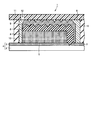
- FIG. 1 is a cross-sectional view schematically showing the structure of a wet solar cell according to an embodiment of the present invention.
- a plurality of first electrodes 3 are formed on the upper surface of a substrate 2 having a light receiving surface that receives sunlight 14.
- the plurality of first electrodes 3 are formed at predetermined intervals.
- the substrate 2 and the first electrode 3 constitute a conductive support 4.
- the sealing part 11 is arrange
- An insulating frame portion 10 is disposed between the first electrode 3 and the sealing portion 11. By surrounding the insulating frame portion 10 on all four sides, a space surrounded by the conductive support 4, the sealing portion 11, and the insulating frame portion 10 is formed.
- the photoelectric conversion unit 5 is formed on the upper surface of the first electrode 3 with a space from the insulating frame 10 in the space.
- the first electrode 3 is formed so as to straddle the adjacent wet solar cells 1.
- the second electrode 9 extends from the upper surface of the first electrode 3 extended from the adjacent wet solar cell 1 toward the sealing portion 11 with an interval from the insulating frame portion 10 in the space. Is formed.
- the second electrode 9 is sealed from the upper surface of the other first electrode 3 adjacent to the first electrode 3 on which the photoelectric conversion unit 5 is formed on the upper surface.
- a second electrode 9 is formed so as to extend toward 11.
- the second electrode 9 has a different extension direction in the vicinity of the sealing portion 11, and a part of the upper surface of the second electrode 9 faces the sealing portion 11.
- a porous insulating portion 6 is disposed between the photoelectric conversion portion 5 and the second electrode 9.
- the porous insulating part 6 insulates between the photoelectric conversion part 5 and the second electrode 9 and between the adjacent first electrodes 3.
- a catalyst portion 7 is formed between the porous insulating portion 6 and the second electrode 9.
- a spacer 13 is formed on the upper surface of the second electrode 9.
- a gap is secured between the second electrode 9 and the sealing portion 11. This gap communicates with the gap between the insulating frame 10 and the photoelectric conversion unit 5 and between the insulating frame 10 and the second electrode 9 in the above space.
- the sealing part 11 is formed with an opening 12 for filling an electrolytic solution that becomes the carrier transporting part 8.
- the opening 12 communicates with the gap between the second electrode 9 and the sealing portion 11.
- the opening 12 communicates with the gap between the insulating frame 10 and the photoelectric conversion unit 5 and between the insulating frame 10 and the second electrode 9.
- the electrolyte is filled into the space through the opening 12 and the gap and the gap.
- the opening 12 is sealed by a sealing member (not shown) after filling with the electrolytic solution.
- the material used as the substrate 2 is a material having heat resistance, electric insulation, and light transmittance with respect to sunlight that can withstand the process temperature when forming the porous semiconductor layer constituting the photoelectric conversion unit 5. If there is no particular limitation.
- a glass substrate, a heat resistant resin plate such as a flexible film, a ceramic substrate, or the like can be used.
- the substrate 2 As the heat resistance of the substrate 2, for example, when a porous semiconductor layer is formed using a paste containing ethyl cellulose, it is preferable that the substrate 2 can withstand about 500 ° C. When the porous semiconductor layer is formed using a paste that does not contain ethyl cellulose, the substrate 2 only needs to have heat resistance that can withstand about 120 ° C.
- substrate 2 is formed from the material with low moisture permeability with respect to this volatile solvent. More preferably, one surface or both surfaces of the substrate 2 are coated with a material having low moisture permeability such as SiO 2 .
- the first electrode 3 has a function of transporting electrons generated in the photoelectric conversion unit 5 to an external circuit.
- the material for forming the first electrode 3 includes ITO (indium-tin composite oxide), tin oxide doped with fluorine, zinc oxide doped with boron, zinc oxide doped with gallium or aluminum, niobium or tantalum.
- a transparent conductive metal oxide such as titanium oxide doped with can be used.
- metals such as gold, silver, aluminum, and indium, carbon such as carbon black, carbon whisker, carbon nanotube, and fullerene can be used.
- a transparent conductive metal oxide is used as a material for forming the first electrode 3.
- a metal or carbon which is an opaque material is used as the first electrode 3, it is preferable to make these materials thin to impart light transmittance.
- the metal corroded by the electrolytic solution used as the carrier transporting portion 8 is used as the first electrode 3, it is preferable to coat the portion of the first electrode 3 that contacts the electrolytic solution with a corrosion resistant material.
- the first electrode 3 is formed on the upper surface of the substrate 2 by sputtering or spraying.
- the film thickness of the first electrode 3 is preferably about 0.02 ⁇ m to 5 ⁇ m.
- the film resistance of the first electrode 3 is preferably as low as possible and is preferably 40 ⁇ / sq or less.
- the first electrode 3 is patterned or the first electrode formed uniformly on the upper surface of the substrate 2 A method of removing a part of 3 is conceivable.
- a method for forming the pattern of the first electrode 3 for example, there are a photolithography method, a method using a metal mask or a tape mask, and the like.
- a method for removing a part of the first electrode 3 there is a chemical method such as solution etching, or a physical method such as laser scribe or sand blaster.
- the photoelectric conversion part 5 is formed by making a photosensitizing dye adsorb
- porous semiconductor layer A porous semiconductor layer is comprised from a semiconductor, The thing of various states, such as a particulate form or a film
- semiconductors such as titanium oxide and zinc oxide can be used alone or in combination of two or more. From the viewpoint of conversion efficiency, stability, and safety, it is preferable to use titanium oxide.
- a method for forming a film-like porous semiconductor layer on the upper surface of the substrate for example, a method of applying a paste containing semiconductor particles on the upper surface of the substrate 2, such as a screen printing method or an ink jet method, and then baking the method. Can be mentioned. From the viewpoint of thickening and manufacturing cost, it is preferable to use a screen printing method using a paste.
- the film thickness of the porous semiconductor layer is not particularly limited, but is preferably about 5 ⁇ m to 50 ⁇ m from the viewpoint of conversion efficiency in the photoelectric conversion unit 5.
- the membrane-like porous semiconductor layer preferably has a large specific surface area, and preferably has a specific surface area of about 10 m 2 / g to 200 m 2 / g.
- the value of the specific surface area shown in this specification is a value measured by the BET adsorption method.
- semiconductor particles for example, single semiconductor or compound semiconductor particles having an average particle diameter of about 1 nm to 500 nm can be used.
- the above-mentioned porous semiconductor layer is dried and fired by appropriately adjusting conditions such as temperature, time, atmosphere, etc., depending on the type of substrate 2 or semiconductor particles used.
- the porous semiconductor layer is dried and fired by being held at a temperature of about 50 ° C. to 800 ° C. for about 10 seconds to 4 hours in the air or an inert gas atmosphere. Drying and baking may be performed in one step under a single temperature, or may be performed in two or more steps at different temperatures.
- Photosensitizing dye examples of the dye that is adsorbed on the porous semiconductor layer and functions as a photosensitizer include one or two dyes such as organic dyes and metal complex dyes having absorption in various visible light regions and / or infrared light regions. More than one species can be selectively used.
- the organic dye for example, azo dyes, quinone dyes, quinone imine dyes, quinacridone dyes, squarylium dyes, cyanine dyes, merocyanine dyes, triphenylmethane dyes, xanthene dyes, porphyrin dyes, perylene System dyes, indigo dyes, naphthalocyanine dyes, and the like can be used.
- the extinction coefficient of an organic dye is generally larger than the extinction coefficient of a metal complex dye that takes a form in which molecules are coordinated to a transition metal.
- metal complex dyes Cu, Ni, Fe, Co, V, Sn, Si, Ti, Ge, Cr, Zn, Ru, Mg, Al, Pb, Mn, In, Mo, Y, Zr, Nb, Sb, Metals such as La, W, Pt, Ta, Ir, Pd, Os, Ga, Tb, Eu, Rb, Bi, Se, As, Sc, Ag, Cd, Hf, Re, Au, Ac, Tc, Te, Rh
- a phthalocyanine dye or a ruthenium dye is used, and a ruthenium metal complex dye is particularly preferable.
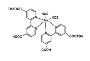
- FIG. 2 is a chemical formula showing a first example of a ruthenium-based metal complex dye preferable as a photosensitizing dye in the present embodiment.
- FIG. 3 is a chemical formula showing a second example of a ruthenium-based metal complex dye preferable as a photosensitizing dye in the present embodiment.
- FIG. 4 is a chemical formula showing a third example of a ruthenium-based metal complex dye that is preferable as a photosensitizing dye in the present embodiment.
- the ruthenium-based metal complex dyes represented by the chemical formulas shown in FIGS. 2 to 4 are particularly preferably used as the photosensitizing dye.
- a carboxylic acid group, a carboxylic acid anhydride group, an alkoxy group, a hydroxyl group, a hydroxyalkyl group, a sulfonic acid is contained in the molecule of the photosensitizing dye. It is preferable that an interlock group such as a group, an ester group, a mercapto group, or a phosphonyl group is included.
- the sensitizing dye molecule preferably contains a carboxylic acid group and a carboxylic acid anhydride group. The interlock group provides an electrical bond that facilitates electron transfer between the excited photosensitizing dye and the conduction band of the porous semiconductor layer.
- the porous semiconductor layer formed on the upper surface of the first electrode 3 is immersed in a solution (dye adsorption solution) in which the photosensitizing dye is dissolved. There is a way to do it.
- the solvent for dissolving the photosensitizing dye may be any solvent that can dissolve the photosensitizing dye.
- alcohols such as ethanol, ketones such as acetone, ethers such as diethyl ether or tetrahydrofuran, Nitrogen compounds such as acetonitrile, halogenated aliphatic hydrocarbons such as chloroform, aliphatic hydrocarbons such as hexane, aromatic hydrocarbons such as benzene, esters such as ethyl acetate, water, and the like can be used. Two or more of these solvents may be mixed and used.
- the concentration of the photosensitizing dye in the solution in which the photosensitizing dye is dissolved is appropriately adjusted depending on the type of the photosensitizing dye and the solvent used. In order to improve the adsorption function of the solution, the photosensitizing dye is used. It is preferable that the concentration of is higher.
- the concentration of the photosensitizing dye is preferably 5 ⁇ 10 ⁇ 4 mol / liter or more.
- the porous insulating part 6 has a function of preventing physical contact and electrical connection between the photoelectric conversion part 5 and the second electrode 9.
- the porous insulating portion 6 must be capable of taking in the electrolyte (redox species) in the carrier transporting portion 8 and moving the electrolyte. Therefore, the porous insulating part 6 is preferably a porous body having continuous bubbles inside the porous insulating part 6.
- the porous insulating part 6 has a high refractive index, and preferably has a function of reflecting the sunlight 14 that has passed through the photoelectric conversion part 5 and causing the light to enter the photoelectric conversion part 5 again. .
- the porous insulating unit 6 having a predetermined thickness is formed on the upper surface of the photoelectric conversion unit 5 without a gap.
- the film may be formed twice or more.
- a high electrical resistance material is used as a material constituting the porous insulating unit 6, or the photoelectric conversion unit 5 is used.
- a method of reducing the contact area between the first electrode 9 and the second electrode 9 is conceivable.
- the high electrical resistance material it is preferable to use an oxide semiconductor, and it is particularly preferable to use a material combining one or more of zirconium oxide, magnesium oxide, aluminum oxide and titanium oxide.
- the contact area between the photoelectric conversion part 5 and the second electrode 9 is reduced, it is preferable to reduce the surface area of the surface of the porous insulating part 6.
- there are methods such as reducing the number of irregularities on the surface of the porous insulating portion 6 or increasing the size of the fine particles used as the material when the porous insulating portion 6 is formed of a porous body. is there.
- a method for forming the porous insulating portion 6 there is a method in which a paste containing semiconductor particles is applied to the upper surface of the conductive support 4 on which the photoelectric conversion portion 5 is formed by a screen printing method, an ink jet method or the like, and then fired. is there.
- the carrier transport portion 8 filled in the space surrounded by the substrate 2, the sealing portion 11 and the insulating frame portion 10 is made of a conductive material capable of transporting ions, for example, an ionic conductor such as an electrolytic solution or a polymer electrolyte.
- an ionic conductor such as an electrolytic solution or a polymer electrolyte.
- an ionic conductor one containing a redox electrolyte is preferable.
- the redox electrolyte specifically, metals such as iron and cobalt, or halogen compounds such as chlorine, bromine and iodine are used.
- iodine When iodine is used as the redox electrolyte, it is not particularly limited as long as it is used in a general battery, but metal iodides such as lithium iodide, sodium iodide, potassium iodide, calcium iodide, It is preferable to use in combination with iodine. Furthermore, an imidazole salt such as dimethylpropylimidazole iodide may be added to iodine.
- carbonate compounds such as propylene carbonate, nitrile compounds such as acetonitrile, alcohols such as ethanol, water, aprotic polar substances, and the like can be used.
- a carbonate compound or a nitrile compound is used. Two or more of these solvents can be mixed and used. If volatilization of the electrolytic solution becomes a problem, a molten salt may be used instead of the solvent.
- the concentration of the redox electrolyte in the carrier transport portion 8 is appropriately selected depending on the type of the electrolyte, but is preferably 0.01 mol / liter or more and 1.5 mol / liter or less.
- the catalyst part 7 has a function of promoting the reaction of the electrolyte (redox species) present in the porous insulating part 6.
- the catalyst part 7 is formed in, for example, a net shape so that the photosensitizing dye can be easily adsorbed on the porous semiconductor layer. It is preferably formed in a shape having a large number of holes.
- the shape of the catalyst part 7 is not particularly limited.
- the catalyst part 7 is formed with the porous body so that the area which contacts a redox seed
- Examples of the material for forming the catalyst portion 7 include Fe, Co, and platinum group Ru elements such as Ru, Rh, Pd, Os, Ir, and Pt, carbons such as carbon black, ketjen black, carbon nanotube, and fullerene, PEDOT / PSS (H) or the like is used.
- Ru elements such as Ru, Rh, Pd, Os, Ir, and Pt
- carbons such as carbon black, ketjen black, carbon nanotube, and fullerene, PEDOT / PSS (H) or the like is used.
- a carbon compound or platinum that is a highly corrosion-resistant material from the viewpoint of long-term stability of the catalyst portion 7. preferable.
- a method for forming the catalyst portion 7 is not particularly limited, and for example, electron beam evaporation or sputtering can be used.
- the second electrode 9 has a function of electrically connecting the catalyst unit 7 of the first wet solar cell 1 and the first electrode 3 of the second wet solar cell 1 adjacent to the first wet solar cell 1.
- a material which forms the 2nd electrode 9 A metal with high electroconductivity or a transparent conductive material can be used.
- a highly corrosive halogen-based redox species is used as the carrier transporting portion 8
- a material having high corrosion resistance for example, a high melting point metal such as Ti or Ta is used from the viewpoint of long-term stability of the second electrode 9.
- the second electrode 9 is preferably used.
- the second electrode 9 is in contact with the carrier transporting portion 8, it is preferable that the second electrode 9 is not formed from a material that promotes redox such as carbon or a platinum group. The reason is that when an oxidation-reduction reaction occurs between the second electrode 9 and the carrier transporting portion 8, an internal short circuit occurs. Therefore, for example, it is preferable to form the second electrode 9 using a material that is a combination of one or more of Ti, Ni, Au, and their compounds (including alloys).
- the second electrode 9 is, for example, Thus, it is preferable to be formed in a shape having a large number of holes.
- the shape of the second electrode 9 is not particularly limited.
- the method for forming the second electrode 9 is not particularly limited, and for example, electron beam evaporation or sputtering can be used.
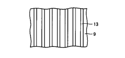
- a spacer 13 is formed on the upper surface of the second electrode 9.
- the spacer 13 may be formed by forming a glass frit on the upper surface of the second electrode 9 using the screen printing method after the second electrode 9 is formed.
- FIG. 5 is a plan view showing a first example of the pattern shape of the spacer according to the present embodiment.
- FIG. 6 is a plan view showing a second example of the pattern shape of the spacer according to the present embodiment.
- FIG. 7 is a plan view showing a third example of the pattern shape of the spacer according to the present embodiment.
- FIG. 8 is a plan view showing a fourth example of the pattern shape of the spacer according to the present embodiment.
- the spacer 13 of the first example is formed on the upper surface of the second electrode 9 in a straight line arranged in parallel at a predetermined interval. In this case, a gap is secured between the straight lines of the spacer 13.
- the spacer 13 of the second example is formed in a dot shape on the upper surface of the second electrode 9 at a predetermined interval. In this case, a gap is secured between the points of the spacer 13.
- the spacer 13 of the third example is formed in a rectangular shape on the upper surface of the second electrode 9 with a predetermined interval therebetween. In this case, a gap is secured between the rectangles of the spacers 13.
- the spacers 13 are arranged so that the upper surface of the second electrode 9 has a mesh shape.
- the spacer 13 of the fourth example is formed in a rectangular shape on the upper surface of the second electrode 9 with a predetermined interval therebetween. In this case as well, a gap is secured between the rectangles of the spacers 13 in the same manner as the spacers 13 of the third example. In the case of the fourth example, the spacers 13 are arranged so that the upper surface of the second electrode 9 has a lattice shape.
- the spacers 13 in the first to fourth examples are preferably formed so as to have a thickness of 0.1 ⁇ m or more.
- the width of the gap between the upper surface of the second electrode 9 and the sealing part 11 is preferably 0.1 ⁇ m or more.
- the width of the gap can be set widely depending on the thickness of the spacer 13. The wider the gap, the more easily the pressure inside the wet solar cell 1 can be reduced, and the carrier transport part 8 can be filled in a short time.
- the gap between the upper surface of the second electrode 9 and the sealing portion 11 is easily filled with the carrier transporting portion 8 depending on the direction of the linear spacer 13, There is a place where it is difficult to fill. Therefore, unevenness may be formed on the upper surface of the spacer 13.
- the concave portion formed on the upper surface of the spacer 13 becomes the flow path of the carrier transport portion 8, the influence of the direction of the linear spacer 13 can be reduced and the carrier transport portion can be uniformly filled. it can.
- the spacer 13 having unevenness on the upper surface can be formed by appropriately changing the nozzle diameter and adjusting the flow rate. Specifically, when forming the convex portion, the nozzle diameter is increased to increase the resin discharge amount, and when forming the concave portion, the nozzle diameter is decreased to reduce the resin discharge amount. Make it smaller.
- FIG. 9 is a cross-sectional view schematically showing the structure of a wet solar cell according to a modification of the present embodiment. As shown in FIG. 9, in the wet solar cell of the modified example, irregularities are formed on the upper surface of the second electrode 9. This unevenness serves as a spacer and secures a gap between the second electrode 9 and the sealing portion 11.
- the porous insulating portion 6 is formed using, for example, zirconium oxide having a particle diameter of 400 nm to 500 nm. In this case, as shown in FIG. 9, unevenness reflecting the particle diameter of zirconium oxide is formed on the upper surface of the porous insulating portion 6.
- the second electrode 9 is formed on the upper surface of the porous insulating portion 6 by evaporating Ti or the like, for example.
- irregularities can be formed on the upper surface of the second electrode 9.
- the unevenness is formed such that the surface roughness Ra of the upper surface of the second electrode 9 is 0.01 ⁇ m or more and 10 ⁇ m or less.
- the unevenness on the upper surface of the second electrode 9 may be constituted by a single particle or an aggregate of fine particles.
- a gap having a width corresponding to the radius of the fine particles is formed between the second electrode 9 and the sealing portion 11. Can be secured between.
- gap can be ensured without providing another member, it is not necessary to increase the number of parts of the wet solar cell 1, and the raise of the manufacturing cost of the wet solar cell 1 can be suppressed.
- the insulating frame part 10 has a function of preventing the movement of the redox species in the carrier transport part 8.
- the insulating frame 10 has an internal short circuit caused by the second electrode 9 contacting the first electrode 3 different from the first electrode 3 connected to the second electrode 9 in the wet solar cell 1. It has a function to prevent the occurrence.
- each wet solar cell is provided by the insulating frame portion 10 so that the redox species in the carrier transport portion 8 are not unevenly distributed. 1 is partitioned. As a result, the movement of the redox species in the carrier transport portion 8 is prevented between the adjacent wet solar cells 1.
- the insulating frame portion 10 is preferably formed of a dense film to such an extent that the redox species in the carrier transporting portion 8 cannot pass through the insulating frame portion 10.
- the dense film may be a film that does not allow redox species to pass between adjacent wet solar cells 1, and includes, for example, a porous body having independent bubbles.
- the insulating frame 10 is formed of an insulating material between the adjacent first electrodes 3 so as not to cause an internal short circuit due to conduction between the adjacent first electrodes 3. As shown in FIG. 1, the insulating frame 10 is arranged so that two sides extend in a direction perpendicular to the drawing sheet.
- an inorganic oxide having a high electrical resistance is generally preferable.
- materials such as silicon oxide, boron oxide, zinc oxide, lead oxide, bismuth oxide, titanium oxide, aluminum oxide, and magnesium oxide can be used as the insulating frame portion 10.
- a method for forming the insulating frame portion 10 a method in which a paste containing semiconductor particles is applied to the upper surface of the conductive support 4 by a screen printing method, an inkjet method, or the like, and then fired can be used.
- the sealing unit 11 has a function of preventing volatilization of the electrolyte solution in the carrier transporting unit 8 and preventing water and the like from entering the wet solar cell 1. Further, the sealing portion 11 has a function of absorbing stress or impact acting on the conductive support 4. Further, the sealing portion 11 has a function of absorbing the deflection generated in the conductive support 4 in the long-term use of the wet solar cell 1.
- the sealing portion 11 As a material for forming the sealing portion 11, for example, a silicon resin, an epoxy resin, a polyisobutylene resin, a hot melt resin, a glass frit, and the like are preferable, and two or more of these are used to be laminated in two or more layers. May be.
- the material for forming the sealing portion 11 is a silicon resin or a hot melt resin (for example, an ionomer resin), a polyisobutylene resin, Glass frit is particularly preferred.
- An opening 12 is formed in the sealing part 11.
- the opening 12 can be provided by a dispenser when the sealing portion 11 is formed using silicon resin, epoxy resin, or glass frit.
- the opening part 12 can be provided by making a hole patterned in the sheet-like hot melt resin.
- the opening 12 serves as an inlet for filling the wet solar cell 1 with the electrolytic solution serving as the carrier transporting portion 8.
- at least one opening 12 is provided at a position that leads to the gap between the insulating frame 10 and the photoelectric conversion unit 5. Further, the position of the opening 12 is preferably formed on the side opposite to the light receiving surface side.
- the wet solar cell module according to this embodiment includes at least one wet solar cell 1 according to this embodiment, and the wet solar cells are connected in series.
- at least one of the wet solar cells 1 constituting the wet solar cell module may be the wet solar cell 1 according to the present embodiment.
- the gaps between the insulating frame 10 and the photoelectric conversion unit 5 and between the insulating frame 10 and the second electrode 9 are Since it leads to the gap formed between the sealing part 11 and the carrier transport part 8, the gap and the gap serve as an air flow path, and the inside of the wet solar cell 1 is easily decompressed. can do.
- the gap and the gap serve as a flow path for the carrier transporting part 8 so that the inside of the wet solar cell 1 can be easily filled with the carrier transporting part 8. Therefore, in the large-area wet solar cell 1, the carrier transport portion 8 can be sufficiently filled in the wet solar cell 1 in a short time.
- the photoelectric conversion unit 5 and the second electrode 9 are formed on the same substrate 2, when sealing the wet solar cell 1 with the sealing unit 11, since the carrier transport part 8 can be sufficiently filled in the wet solar cell 1 while maintaining the relative position between the photoelectric conversion part 5 and the second electrode 9, the power generation performance of the wet solar cell 1 is improved. be able to.
- a wet solar cell constituting the monolithic dye-sensitized solar cell module shown in FIG. 13 was produced.
- a conductive glass substrate manufactured by Nippon Sheet Glass Co., Ltd., trade name: glass with SnO 2 film, length 1510 mm ⁇ width 15 mm
- a titanium oxide paste manufactured by Solaronix, product name: Ti-Nanoxide D / SP
- Film formation was performed using a printing machine (LS-150 manufactured by Neurong Seimitsu Kogyo).
- the porous glass layer was formed by baking the conductive glass substrate at a temperature of 500 ° C. for 60 minutes.
- a paste containing zirconia particles having an average particle size of 50 nm was formed on the porous semiconductor layer by using the screen printing machine.
- This conductive glass substrate was baked at a temperature of 500 ° C. for 60 minutes to form a porous insulating portion having a flat portion with a thickness of 7 ⁇ m.
- Both a Pt film having a thickness of 50 nm as a catalyst layer and a Ti film having a thickness of 300 nm as a second electrode were formed using an electron beam vapor deposition machine.
- a ruthenium dye having a chemical formula shown in FIG. 4 (trade name: Ruthenium 620-1H3TBA, manufactured by Solaronix) and a solvent in which acetonitrile and 1-butanol are mixed at a volume ratio of 1: 1, the concentration is 4 ⁇ 10 ⁇ 4 mol /
- the dye solution for adsorption was prepared by dissolving to 1 liter.
- the conductive glass substrate having the porous semiconductor layer was immersed in the dye solution for adsorption so that the dye was adsorbed on the porous semiconductor layer (titanium oxide film). Thereafter, the conductive glass substrate taken out from the dye solution for adsorption was washed with ethanol (manufactured by Aldrich Chemical Company) and dried to form a photoelectric conversion part.
- a photosensitive resin manufactured by Three Bond: 31X-101
- a dispenser manufactured by EFD: ULTRASAVER
- EFD ULTRASAVER
- the photosensitive resin was cured by irradiating the conductive glass substrate with ultraviolet rays using an ultraviolet lamp (manufactured by EFD: NOVACURE).
- EFD NOVACURE
- the distance between the second electrode and the sealing portion was 5 ⁇ m, and the photosensitive resin was formed so that no gap was formed in the space between the conductive glass substrate and the sealing portion.
- the inside of the wet solar cell was depressurized through four electrolyte depressurization times of 30, 120, 450, and 1800 seconds through the electrolyte injection port formed in the sealing portion. Thereafter, an electrolytic solution was injected by a capillary effect. After injecting the electrolyte solution, the electrolyte injection port was sealed with a photosensitive resin to prepare a wet solar cell.
- the electrolyte used as the carrier transporting part was acetonitrile (manufactured by Aldrich Chemical Company), lithium iodide with a concentration of 0.1 mol / liter (manufactured by Aldrich Chemical Company), and iodine with a concentration of 0.01 mol / liter (Aldrich). Chemical Company), concentration is 0. 5 mol / liter TBP (manufactured by Aldrich Chemical Company) and dimethylpropylimidazole iodide (manufactured by Shikoku Kasei) having a concentration of 0.6 mol / liter were prepared.
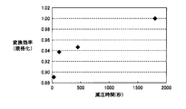
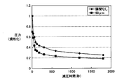
- FIG. 10 is a graph showing the relationship between the decompression time in the wet solar cell and the conversion efficiency of the wet solar cell in Experimental Example 1.
- the vertical axis represents the conversion efficiency of the wet solar cell
- the horizontal axis represents the decompression time in the wet solar cell.
- conversion efficiency was confirmed by irradiating the wet solar cell with artificial sunlight of AM (Air Mass) 1.5 and irradiation intensity of 100 mW / cm 2 .
- the conversion efficiency of the wet solar cell is higher as the depressurization time in the wet solar cell is longer. It is possible to reduce the pressure to the details of the porous body in the wet solar cell by lengthening the decompression time. As a result, when filling the electrolyte in the wet solar cell, the electrolyte to the details of the porous body. This is because it penetrates.
- Experimental example 2 A gap is formed between the sealing portion and the second electrode in the conventional wet solar cell in the case where a gap is formed between the sealing portion and the second electrode as in the wet solar cell of the present embodiment.
- the pressure change in the wet solar cell due to the pressure reduction time in the wet solar cell in the case of not performing was confirmed.
- the wet solar cell produced in Experimental Example 1 was used as a wet solar cell in which no gap was formed between the sealing portion and the second electrode.
- glass frit was screen-printed on the upper surface of the second electrode so as to have the pattern shown in FIG.
- the width of the gap formed between the upper surface of the second electrode and the sealing portion was set to 50 ⁇ m.
- FIG. 11 is a graph showing the relationship between the pressure reduction time in the wet solar cell and the pressure in the wet solar cell in Experimental Example 2.
- the vertical axis represents the pressure in the wet solar cell normalized, and the horizontal axis represents the pressure reduction time in the wet solar cell.
- the pressure in the wet solar cell indicates a relative pressure where the pressure when the pressure reduction time in the wet solar cell is 0 is 1.
- the pressure in the wet solar cell was confirmed by a Pirani gauge connected to the wet solar cell.
- the inside of the wet solar cell can be depressurized in a shorter time when a gap is formed between the second electrode and the sealing portion. This is because the gap plays a role of an air flow path.
- the irregularities When forming irregularities on the upper surface of the second electrode, the irregularities may be formed on the entire upper surface of the second electrode, or irregularities may be formed only on a part thereof.
- the spacer When forming the spacer on the upper surface of the second electrode, the spacer may be formed on the entire upper surface of the second electrode, or the spacer may be formed only on a part thereof. Also, the spacer pattern can be changed as appropriate.
- the surface roughness Ra of the upper surface of the second electrode is 0.01 ⁇ m or more in order to ensure a void in which the electrolyte can be easily injected into the wet solar cell. Is preferred. More preferably, the surface roughness Ra of the upper surface of the second electrode is 0.01 ⁇ m or more and 10 ⁇ m or less. In this case, as shown in FIG. 9, irregularities can be easily formed on the upper surface of the second electrode by selecting the particle size of the material forming the porous insulating portion.
- the present invention is a technique for facilitating pressure reduction inside a wet solar cell and injection of an electrolyte into the wet solar cell. Therefore, the method for manufacturing a wet solar cell described in the embodiment is an example, and in a wet solar cell manufactured by another method, the pressure reduction inside the wet solar cell and the electrolyte solution inside the wet solar cell A wet solar cell in which a void that facilitates injection is formed in the present invention.
Abstract
Description
(基板2)
基板2として用いられる材料は、光電変換部5を構成する多孔性半導体層を形成する際のプロセス温度に耐えうる耐熱性、電気絶縁性、および、太陽光に対して光透過性を有する材料であれば特に限定されない。たとえば、ガラス基板、可撓性フィルムなどの耐熱性樹脂板、または、セラミック基板などを用いることができる。 Hereinafter, each component of the wet
(Substrate 2)
The material used as the
第1電極3は、光電変換部5で発生した電子を外部回路に輸送する機能を有している。第1電極3を形成する材料としては、ITO(インジウム-スズ複合酸化物)、フッ素がドープされた酸化スズ、ボロンがドープされた酸化亜鉛、ガリウムまたはアルミニウムがドープされた酸化亜鉛、ニオブまたはタンタルがドープされた酸化チタンなどの透明導電性金属酸化物を用いることができる。また、第1電極3を形成する材料としては、金、銀、アルミニウム、インジウムなどの金属、カーボンブラック、カーボンホイスカ、カーボンナノチューブ、フラーレンなどのカーボンを用いることができる。 (First electrode 3)
The first electrode 3 has a function of transporting electrons generated in the
光電変換部5は、多孔性半導体層に光増感色素を吸着させることで形成される。 (Photoelectric converter 5)
The
多孔性半導体層は、半導体から構成され、その状態は、粒子状または膜状などの種々な状態のものを用いることができる。好ましくは、膜状の状態の半導体が用いられる。多孔性半導体層を構成する材料としては、酸化チタン、酸化亜鉛などの半導体を1種類または2種類以上組み合わせて用いることができる。変換効率、安定性、安全性の観点から、酸化チタンを用いることが好ましい。 (Porous semiconductor layer)
A porous semiconductor layer is comprised from a semiconductor, The thing of various states, such as a particulate form or a film | membrane form, can be used for the state. Preferably, a film-like semiconductor is used. As a material constituting the porous semiconductor layer, semiconductors such as titanium oxide and zinc oxide can be used alone or in combination of two or more. From the viewpoint of conversion efficiency, stability, and safety, it is preferable to use titanium oxide.
多孔性半導体層に吸着されて光増感剤として機能する色素としては、種々の可視光領域および/または赤外光領域に吸収をもつ、有機色素または金属錯体色素などの色素から1種または2種以上を選択的に用いることができる。 (Photosensitizing dye)
Examples of the dye that is adsorbed on the porous semiconductor layer and functions as a photosensitizer include one or two dyes such as organic dyes and metal complex dyes having absorption in various visible light regions and / or infrared light regions. More than one species can be selectively used.
多孔性絶縁部6は、光電変換部5と第2電極9との物理的接触および電気的接続を阻止する機能を有している。多孔性絶縁部6としては、キャリア輸送部8中の電解質(酸化還元種)を内部に取り込み、かつ、電解質を移動させることができるものでなければならない。そのため、多孔性絶縁部6は、多孔性絶縁部6の内部に、連続した気泡を有する多孔体であることが好ましい。さらに、多孔性絶縁部6は、屈折率が高く、光電変換部5を通り抜けた太陽光14を反射して、光を再び光電変換部5の内部に入射させる機能を有していることが好ましい。 (Porous insulation part 6)
The porous
基板2、封止部11および絶縁枠部10により囲まれる空間に充填されるキャリア輸送部8は、イオンを輸送できる導電性材料、たとえば、電解液、高分子電解質などのイオン導電体から構成される。このイオン導電体としては、酸化還元性電解質を含むものが好ましい。酸化還元性電解質として、具体的には、鉄系、コバルト系などの金属類、または、塩素、臭素、ヨウ素などのハロゲン化合物が用いられる。 (Carrier Transport Department 8)
The
触媒部7は、多孔性絶縁部6中に存在する電解質(酸化還元種)の反応を促進する機能を有している。多孔性半導体層に光増感色素を吸着させる前に触媒部7を形成する場合、多孔性半導体層に光増感色素を吸着させ易くなるように、触媒部7は、たとえば、網状のように多数の孔を有する形状に形成されていることが好ましい。多孔性半導体層に光増感色素を吸着させた後に触媒部7を形成する場合は、触媒部7の形状は特に限られない。また、触媒部7は、酸化還元種と接触する面積が大きくなるように、多孔体で形成されていることが好ましい。 (Catalyst part 7)
The
第2電極9は、第1の湿式太陽電池1の触媒部7と、第1の湿式太陽電池1に隣接する第2の湿式太陽電池1の第1電極3とを電気的に接続する機能を有している。第2電極9を形成する材料としては、特に限定されないが、導電性が高い金属または透明導電性材料を用いることができる。ただし、キャリア輸送部8として腐食性の高いハロゲン系の酸化還元種を用いる場合には、第2電極9の長期安定性の観点から耐食性の高い材料、たとえば、TiまたはTaなどの高融点金属を第2電極9として用いることが好ましい。 (Second electrode 9)
The
絶縁枠部10は、キャリア輸送部8の酸化還元種の移動を阻止する機能を有している。また、絶縁枠部10は、湿式太陽電池1内において、第2電極9が、第2電極9と接続されている第1電極3とは異なる第1電極3に接触することにより、内部短絡が生ずることを防止する機能を有している。 (Insulation frame 10)
The insulating
封止部11は、キャリア輸送部8の電解液の揮発の防止、および、湿式太陽電池1の内部への水などの浸入を防止する機能を有している。また、封止部11は、導電性支持体4に作用する応力または衝撃を吸収する機能を有している。さらに、封止部11は、湿式太陽電池1の長期にわたる使用において、導電性支持体4に発生するたわみなどを吸収する機能を有している。 (Sealing part 11)
The sealing
開口部12は、キャリア輸送部8である電解液の湿式太陽電池1への充填入口となる。本実施形態においては、絶縁枠部10と光電変換部5との隙間に通じる位置に、少なくとも一つの開口部12を設けている。また、開口部12の位置としては、受光面側とは反対側に形成されていることが好ましい。 (Opening 12)
The
本実施形態に係る湿式太陽電池モジュールは、本実施形態に係る湿式太陽電池1を少なくとも1つ含み、湿式太陽電池が直列に接続されて構成されている。言い換えると、湿式太陽電池モジュールを構成する少なくとも2つ以上の湿式太陽電池の中で、少なくとも1つが本実施形態に係る湿式太陽電池1であればよい。 (Wet solar cell module)
The wet solar cell module according to this embodiment includes at least one wet
従来の湿式太陽電池において、湿式太陽電池内の減圧時間と湿式太陽電池の変換効率との関係を確認した。以下、本実験方法について説明する。 Experimental example 1
In the conventional wet solar cell, the relationship between the decompression time in the wet solar cell and the conversion efficiency of the wet solar cell was confirmed. Hereinafter, this experimental method will be described.
本実施形態の湿式太陽電池のように、封止部と第2電極との間に空隙を形成した場合と、従来の湿式太陽電池において、封止部と第2電極との間に空隙を形成しない場合とにおける、湿式太陽電池内の減圧時間による湿式太陽電池内の圧力変化を確認した。 Experimental example 2
A gap is formed between the sealing portion and the second electrode in the conventional wet solar cell in the case where a gap is formed between the sealing portion and the second electrode as in the wet solar cell of the present embodiment. The pressure change in the wet solar cell due to the pressure reduction time in the wet solar cell in the case of not performing was confirmed.
多孔性絶縁部、7 触媒部、8 キャリア輸送部、9 第2電極、10 絶縁枠部、11 封止部、12 開口部、13 スペーサ、14 太陽光、21,22,31 ガラス基板、23,35 対極、24,33 光電変換部、25,32 透明導電膜、26 キャリア輸送部、27 絶縁性保護部、28 導電性接続部、34 多孔性絶縁部、36 絶縁部、37 絶縁性トップカバー。 DESCRIPTION OF
Porous insulating part, 7 catalyst part, 8 carrier transport part, 9 second electrode, 10 insulating frame part, 11 sealing part, 12 opening part, 13 spacer, 14 sunlight, 21, 22, 31 glass substrate, 23, 35 Counter electrode, 24, 33 Photoelectric conversion part, 25, 32 Transparent conductive film, 26 Carrier transport part, 27 Insulating protective part, 28 Conductive connection part, 34 Porous insulating part, 36 Insulating part, 37 Insulating top cover.
Claims (8)
- 受光面を有する基板(2)と、
前記基板(2)に対向して配置される封止部(11)と、
前記基板(2)の前記封止部(11)に対向する側の面の上面に形成された第1電極(3)と、
前記第1電極(3)と前記封止部(11)との間に配置され、内部に空間が形成されるように四方を囲む絶縁枠部(10)と、
前記空間内において前記絶縁枠部(10)に対して間隔を開けて、前記第1電極(3)の上面に形成された光電変換部(5)と、
前記空間内において、前記第1電極(3)に隣接する他の第1電極(3)の上面から前記封止部(11)に向けて延在するように形成され、上面の一部が前記封止部(11)に対向する第2電極(9)と、
前記光電変換部(5)と前記第2電極(9)との間に配置され、前記光電変換部(5)と前記第2電極(9)との間、および、隣接する前記第1電極(3)同士の間を絶縁する多孔性絶縁部(6)と
を備え、
前記空間内において、前記絶縁枠部(10)と前記光電変換部(5)との間に通じる空隙が、前記第2電極(9)と前記封止部(11)との間に形成され、
前記空隙を含む前記空間の内部がキャリア輸送部(8)により充填された、湿式太陽電池(1)。 A substrate (2) having a light receiving surface;
A sealing portion (11) disposed opposite to the substrate (2);
A first electrode (3) formed on the upper surface of the surface of the substrate (2) facing the sealing portion (11);
An insulating frame portion (10) disposed between the first electrode (3) and the sealing portion (11) and surrounding the four sides so as to form a space inside;
A photoelectric conversion part (5) formed on the upper surface of the first electrode (3) at a distance from the insulating frame part (10) in the space;
In the space, the first electrode (3) adjacent to the first electrode (3) is formed so as to extend from the upper surface of the other first electrode (3) toward the sealing portion (11), and a part of the upper surface is formed as described above. A second electrode (9) facing the sealing portion (11);
The first electrode (5) disposed between the photoelectric conversion unit (5) and the second electrode (9), between the photoelectric conversion unit (5) and the second electrode (9) and adjacent to the first electrode ( 3) a porous insulating part (6) that insulates each other;
In the space, a gap communicating between the insulating frame part (10) and the photoelectric conversion part (5) is formed between the second electrode (9) and the sealing part (11),
A wet solar cell (1) in which the inside of the space including the gap is filled with a carrier transporting part (8). - 前記空隙が、前記第2電極(9)の上面の凹凸により形成される、請求の範囲第1項に記載の湿式太陽電池。 The wet solar cell according to claim 1, wherein the gap is formed by irregularities on the upper surface of the second electrode (9).
- 前記空隙が、前記第2電極(9)の上面に形成されたスペーサ(13)により形成される、請求の範囲第1項に記載の湿式太陽電池。 The wet solar cell according to claim 1, wherein the gap is formed by a spacer (13) formed on an upper surface of the second electrode (9).
- 前記スペーサ(13)が、平面的に見て、前記第2電極(9)の上面に直線状に形成された複数のパターンから構成されている、請求の範囲第3項に記載の湿式太陽電池。 The wet solar cell according to claim 3, wherein the spacer (13) is composed of a plurality of patterns formed linearly on the upper surface of the second electrode (9) when viewed in plan. .
- 前記スペーサ(13)が、平面的に見て、前記第2電極(9)の上面に点状に形成された複数のパターンから構成されている、請求の範囲第3項に記載の湿式太陽電池。 The wet solar cell according to claim 3, wherein the spacer (13) is composed of a plurality of patterns formed in a dotted pattern on the upper surface of the second electrode (9) when viewed in plan. .
- 前記スペーサ(13)が、平面的に見て、前記第2電極(9)の上面に、互いに所定の間隔を開けて矩形状に形成されたパターンから構成されている、請求の範囲第3項に記載の湿式太陽電池。 The said spacer (13) is comprised from the pattern formed in the rectangular shape at predetermined intervals on the upper surface of the said 2nd electrode (9) seeing planarly, Claim 3 The wet solar cell according to 1.
- 前記凹凸が、微粒子単体または微粒子の集合体から形成されている、請求の範囲第2項に記載の湿式太陽電池。 3. The wet solar cell according to claim 2, wherein the unevenness is formed from a single particle or an aggregate of particles.
- 請求の範囲第1項から第7項のいずれかに記載の湿式太陽電池を含む、複数の湿式太陽電池が互いに接続された、湿式太陽電池モジュール。 A wet solar cell module in which a plurality of wet solar cells including the wet solar cell according to any one of claims 1 to 7 are connected to each other.
Priority Applications (4)
| Application Number | Priority Date | Filing Date | Title |
|---|---|---|---|
| JP2011538500A JP5456054B2 (en) | 2009-11-02 | 2010-10-29 | Wet solar cell and wet solar cell module |
| EP10826861.6A EP2498330A4 (en) | 2009-11-02 | 2010-10-29 | Wet solar cell and wet solar cell module |
| US13/502,677 US20120211048A1 (en) | 2009-11-02 | 2010-10-29 | Wet solar cell and wet solar cell module |
| CN201080049010.4A CN102598402B (en) | 2009-11-02 | 2010-10-29 | Wet solar cell and wet solar cell module |
Applications Claiming Priority (2)
| Application Number | Priority Date | Filing Date | Title |
|---|---|---|---|
| JP2009252104 | 2009-11-02 | ||
| JP2009-252104 | 2009-11-02 |
Publications (1)
| Publication Number | Publication Date |
|---|---|
| WO2011052731A1 true WO2011052731A1 (en) | 2011-05-05 |
Family
ID=43922153
Family Applications (1)
| Application Number | Title | Priority Date | Filing Date |
|---|---|---|---|
| PCT/JP2010/069309 WO2011052731A1 (en) | 2009-11-02 | 2010-10-29 | Wet solar cell and wet solar cell module |
Country Status (5)
| Country | Link |
|---|---|
| US (1) | US20120211048A1 (en) |
| EP (1) | EP2498330A4 (en) |
| JP (1) | JP5456054B2 (en) |
| CN (1) | CN102598402B (en) |
| WO (1) | WO2011052731A1 (en) |
Cited By (3)
| Publication number | Priority date | Publication date | Assignee | Title |
|---|---|---|---|---|
| WO2012070562A1 (en) * | 2010-11-24 | 2012-05-31 | シャープ株式会社 | Photoelectric transducer and production method therefor |
| JP2013109952A (en) * | 2011-11-21 | 2013-06-06 | Dainippon Printing Co Ltd | Flexible solar cell element module |
| US20130180582A1 (en) * | 2012-01-17 | 2013-07-18 | Mke Technologies Co. Ltd | Dye sensitized solar cell |
Families Citing this family (5)
| Publication number | Priority date | Publication date | Assignee | Title |
|---|---|---|---|---|
| KR102061922B1 (en) | 2012-02-23 | 2020-01-02 | 트레드스톤 테크놀로지스, 인크. | Corrosion resistant and electrically conductive surface of metal |
| CN104380408B (en) * | 2012-09-01 | 2017-02-22 | 株式会社藤仓 | Dye-sensitized solar cell element |
| TW201620150A (en) * | 2014-10-14 | 2016-06-01 | Sekisui Chemical Co Ltd | Solar cell |
| BR112017007730B1 (en) * | 2014-10-14 | 2022-06-14 | Sekisui Chemical Co., Ltd | SOLAR CELL |
| DE102018132342A1 (en) * | 2018-12-14 | 2020-06-18 | Heliatek Gmbh | Stabilization of laser structured organic photovoltaics |
Citations (10)
| Publication number | Priority date | Publication date | Assignee | Title |
|---|---|---|---|---|
| JPH01220380A (en) | 1988-02-12 | 1989-09-04 | Gebr Sulzer Ag | Photoelectrochemical battery and its manufacture |
| WO1997016838A1 (en) | 1995-10-31 | 1997-05-09 | Ecole Polytechnique Federale De Lausanne | A battery of photovoltaic cells and process for manufacturing the same |
| JP2001357897A (en) | 2000-06-14 | 2001-12-26 | Fuji Xerox Co Ltd | Photoelectric conversion module |
| JP2002075472A (en) * | 2000-08-25 | 2002-03-15 | Sharp Corp | Color solar cell and manufacturing method of the same |
| JP2005056613A (en) * | 2003-08-07 | 2005-03-03 | Sharp Corp | Dye sensitized solar battery and module thereof |
| JP2005235725A (en) | 2004-01-20 | 2005-09-02 | Sharp Corp | Dye-sensitized solar cell module |
| JP2006244954A (en) | 2005-03-07 | 2006-09-14 | Fujimori Kogyo Co Ltd | Wiring connection structure of dye-sensitized solar battery cell and dye-sensitized solar cell module |
| JP2006269168A (en) | 2005-03-23 | 2006-10-05 | Kyocera Corp | Photoelectric conversion device, its manufacturing method, and optical power generation device |
| JP2007059181A (en) | 2005-08-24 | 2007-03-08 | Sony Corp | Optical device and manufacturing method therefor |
| JP2009252575A (en) * | 2008-04-08 | 2009-10-29 | Sharp Corp | Paste for dye-sensitized solar cell, transparent insulating film for dye-sensitized solar cell, dye-sensitized solar cell, and dye-sensitized solar cell fabrication method |
Family Cites Families (11)
| Publication number | Priority date | Publication date | Assignee | Title |
|---|---|---|---|---|
| US7586035B2 (en) * | 2004-02-19 | 2009-09-08 | Konarka Technologies, Inc. | Photovoltaic cell with spacers |
| SE521683C2 (en) * | 2000-06-14 | 2003-11-25 | Ivf Industriforskning Och Utve | Method of Manufacture of Sealed Monolithic Electrochemical Systems and Sealed Monolithic Electrochemical System |
| WO2008139479A2 (en) * | 2007-05-15 | 2008-11-20 | 3Gsolar Ltd. | Photovoltaic cell |
| KR100499051B1 (en) * | 2003-06-25 | 2005-07-04 | 한국전자통신연구원 | Dye-sensitized solar cells including liquid type imidazolium electrolyte |
| EP1677316A4 (en) * | 2003-10-23 | 2009-08-26 | Bridgestone Corp | Transparent conductive substrate, electrode for dye-sensitized solar cell and dye-sensitized solar cell |
| JP4914660B2 (en) * | 2006-07-06 | 2012-04-11 | シャープ株式会社 | Dye-sensitized solar cell module and manufacturing method thereof |
| JP5046630B2 (en) * | 2006-12-07 | 2012-10-10 | シャープ株式会社 | Photoelectric conversion element and dye-sensitized solar cell |
| JP5078367B2 (en) * | 2007-01-17 | 2012-11-21 | 京セラ株式会社 | PHOTOELECTRIC CONVERSION DEVICE, MANUFACTURING METHOD THEREOF, AND PHOTOVOLTAIC GENERATION DEVICE |
| CN101682100B (en) * | 2007-06-06 | 2012-08-29 | 株式会社藤仓 | Dye-sensitized solar battery module and method for manufacturing the same |
| US20110036404A1 (en) * | 2008-04-25 | 2011-02-17 | Kyocera Corporation | Photoelectric Conversion Device and Photovoltaic Power Generation Device |
| CN102396101B (en) * | 2009-04-15 | 2014-06-25 | 夏普株式会社 | Dye-sensitized solar cell and dye-sensitized solar cell module |
-
2010
- 2010-10-29 WO PCT/JP2010/069309 patent/WO2011052731A1/en active Application Filing
- 2010-10-29 JP JP2011538500A patent/JP5456054B2/en not_active Expired - Fee Related
- 2010-10-29 US US13/502,677 patent/US20120211048A1/en not_active Abandoned
- 2010-10-29 EP EP10826861.6A patent/EP2498330A4/en not_active Ceased
- 2010-10-29 CN CN201080049010.4A patent/CN102598402B/en not_active Expired - Fee Related
Patent Citations (10)
| Publication number | Priority date | Publication date | Assignee | Title |
|---|---|---|---|---|
| JPH01220380A (en) | 1988-02-12 | 1989-09-04 | Gebr Sulzer Ag | Photoelectrochemical battery and its manufacture |
| WO1997016838A1 (en) | 1995-10-31 | 1997-05-09 | Ecole Polytechnique Federale De Lausanne | A battery of photovoltaic cells and process for manufacturing the same |
| JP2001357897A (en) | 2000-06-14 | 2001-12-26 | Fuji Xerox Co Ltd | Photoelectric conversion module |
| JP2002075472A (en) * | 2000-08-25 | 2002-03-15 | Sharp Corp | Color solar cell and manufacturing method of the same |
| JP2005056613A (en) * | 2003-08-07 | 2005-03-03 | Sharp Corp | Dye sensitized solar battery and module thereof |
| JP2005235725A (en) | 2004-01-20 | 2005-09-02 | Sharp Corp | Dye-sensitized solar cell module |
| JP2006244954A (en) | 2005-03-07 | 2006-09-14 | Fujimori Kogyo Co Ltd | Wiring connection structure of dye-sensitized solar battery cell and dye-sensitized solar cell module |
| JP2006269168A (en) | 2005-03-23 | 2006-10-05 | Kyocera Corp | Photoelectric conversion device, its manufacturing method, and optical power generation device |
| JP2007059181A (en) | 2005-08-24 | 2007-03-08 | Sony Corp | Optical device and manufacturing method therefor |
| JP2009252575A (en) * | 2008-04-08 | 2009-10-29 | Sharp Corp | Paste for dye-sensitized solar cell, transparent insulating film for dye-sensitized solar cell, dye-sensitized solar cell, and dye-sensitized solar cell fabrication method |
Non-Patent Citations (1)
| Title |
|---|
| See also references of EP2498330A4 * |
Cited By (4)
| Publication number | Priority date | Publication date | Assignee | Title |
|---|---|---|---|---|
| WO2012070562A1 (en) * | 2010-11-24 | 2012-05-31 | シャープ株式会社 | Photoelectric transducer and production method therefor |
| JP5956929B2 (en) * | 2010-11-24 | 2016-07-27 | シャープ株式会社 | Photoelectric conversion element and manufacturing method thereof |
| JP2013109952A (en) * | 2011-11-21 | 2013-06-06 | Dainippon Printing Co Ltd | Flexible solar cell element module |
| US20130180582A1 (en) * | 2012-01-17 | 2013-07-18 | Mke Technologies Co. Ltd | Dye sensitized solar cell |
Also Published As
| Publication number | Publication date |
|---|---|
| US20120211048A1 (en) | 2012-08-23 |
| EP2498330A1 (en) | 2012-09-12 |
| JP5456054B2 (en) | 2014-03-26 |
| CN102598402B (en) | 2014-09-03 |
| CN102598402A (en) | 2012-07-18 |
| EP2498330A4 (en) | 2014-08-20 |
| JPWO2011052731A1 (en) | 2013-03-21 |
Similar Documents
| Publication | Publication Date | Title |
|---|---|---|
| JP5456054B2 (en) | Wet solar cell and wet solar cell module | |
| JP5002595B2 (en) | Dye-sensitized solar cell module and manufacturing method thereof | |
| JP5367817B2 (en) | Wet solar cell module | |
| JP4914660B2 (en) | Dye-sensitized solar cell module and manufacturing method thereof | |
| JP5273709B2 (en) | Dye-sensitized solar cell, method for producing the same, and dye-sensitized solar cell module | |
| EP2043191A1 (en) | Dye-sensitized solar cell module and method for fabricating same | |
| EP2525437B1 (en) | Wet-type solar battery and wet-type solar battery module | |
| JP2007194039A (en) | Dye-sensitized solar cell and module thereof | |
| EP2581981B1 (en) | Wet-type solar cell and wet-type solar cell module | |
| JP4881600B2 (en) | Dye-sensitized solar cell, method for producing the same, and dye-sensitized solar cell module | |
| JP4868782B2 (en) | Dye-sensitized solar cell module and manufacturing method thereof | |
| JP5162346B2 (en) | Dye-sensitized solar cell, method for producing the same, and dye-sensitized solar cell module | |
| JP5162347B2 (en) | Dye-sensitized solar cell, method for producing the same, and dye-sensitized solar cell module | |
| JP2012009374A (en) | Dye-sensitized solar cell and its manufacturing method, and dye-sensitized solar cell module | |
| JP4892186B2 (en) | Dye-sensitized solar cell and dye-sensitized solar cell module | |
| WO2013164967A1 (en) | Photoelectric conversion element and photoelectric conversion module | |
| JP2009043482A (en) | Dye-sensitized solar cell, and dye-sensitized solar cell module | |
| JP6050247B2 (en) | Wet solar cell and wet solar cell module | |
| JP5758400B2 (en) | Dye-sensitized solar cell module and manufacturing method thereof | |
| JP2007157490A (en) | Photoelectric conversion element and photoelectric conversion element module | |
| JP2013200960A (en) | Photoelectric conversion element module and manufacturing method thereof | |
| WO2013161557A1 (en) | Photoelectric conversion element module and method for manufacturing same | |
| KR20110050018A (en) | Fabrication method of dye-sensitized solar cell |
Legal Events
| Date | Code | Title | Description |
|---|---|---|---|
| WWE | Wipo information: entry into national phase |
Ref document number: 201080049010.4 Country of ref document: CN |
|
| 121 | Ep: the epo has been informed by wipo that ep was designated in this application |
Ref document number: 10826861 Country of ref document: EP Kind code of ref document: A1 |
|
| WWE | Wipo information: entry into national phase |
Ref document number: 2011538500 Country of ref document: JP |
|
| WWE | Wipo information: entry into national phase |
Ref document number: 13502677 Country of ref document: US |
|
| NENP | Non-entry into the national phase |
Ref country code: DE |
|
| REEP | Request for entry into the european phase |
Ref document number: 2010826861 Country of ref document: EP |
|
| WWE | Wipo information: entry into national phase |
Ref document number: 2010826861 Country of ref document: EP |