WO2011024795A1 - 電子デバイス及びこれを備えた膜濾過装置 - Google Patents
電子デバイス及びこれを備えた膜濾過装置 Download PDFInfo
- Publication number
- WO2011024795A1 WO2011024795A1 PCT/JP2010/064260 JP2010064260W WO2011024795A1 WO 2011024795 A1 WO2011024795 A1 WO 2011024795A1 JP 2010064260 W JP2010064260 W JP 2010064260W WO 2011024795 A1 WO2011024795 A1 WO 2011024795A1
- Authority
- WO
- WIPO (PCT)
- Prior art keywords
- electronic device
- resin
- circuit board
- wireless communication
- crystal resonator
- Prior art date
- Legal status (The legal status is an assumption and is not a legal conclusion. Google has not performed a legal analysis and makes no representation as to the accuracy of the status listed.)
- Ceased
Links
- 0 CCCCC(CC(C)C(C)CC1)C1[C@@](C(C)C)C(CC)=C(C1*(C)C1)N=O Chemical compound CCCCC(CC(C)C(C)CC1)C1[C@@](C(C)C)C(CC)=C(C1*(C)C1)N=O 0.000 description 1
Images


Classifications
-
- C—CHEMISTRY; METALLURGY
- C02—TREATMENT OF WATER, WASTE WATER, SEWAGE, OR SLUDGE
- C02F—TREATMENT OF WATER, WASTE WATER, SEWAGE, OR SLUDGE
- C02F1/00—Treatment of water, waste water, or sewage
- C02F1/44—Treatment of water, waste water, or sewage by dialysis, osmosis or reverse osmosis
-
- B—PERFORMING OPERATIONS; TRANSPORTING
- B01—PHYSICAL OR CHEMICAL PROCESSES OR APPARATUS IN GENERAL
- B01D—SEPARATION
- B01D61/00—Processes of separation using semi-permeable membranes, e.g. dialysis, osmosis or ultrafiltration; Apparatus, accessories or auxiliary operations specially adapted therefor
- B01D61/02—Reverse osmosis; Hyperfiltration ; Nanofiltration
- B01D61/12—Controlling or regulating
-
- B—PERFORMING OPERATIONS; TRANSPORTING
- B01—PHYSICAL OR CHEMICAL PROCESSES OR APPARATUS IN GENERAL
- B01D—SEPARATION
- B01D61/00—Processes of separation using semi-permeable membranes, e.g. dialysis, osmosis or ultrafiltration; Apparatus, accessories or auxiliary operations specially adapted therefor
- B01D61/14—Ultrafiltration; Microfiltration
- B01D61/22—Controlling or regulating
-
- B—PERFORMING OPERATIONS; TRANSPORTING
- B01—PHYSICAL OR CHEMICAL PROCESSES OR APPARATUS IN GENERAL
- B01D—SEPARATION
- B01D65/00—Accessories or auxiliary operations, in general, for separation processes or apparatus using semi-permeable membranes
-
- H—ELECTRICITY
- H05—ELECTRIC TECHNIQUES NOT OTHERWISE PROVIDED FOR
- H05K—PRINTED CIRCUITS; CASINGS OR CONSTRUCTIONAL DETAILS OF ELECTRIC APPARATUS; MANUFACTURE OF ASSEMBLAGES OF ELECTRICAL COMPONENTS
- H05K3/00—Apparatus or processes for manufacturing printed circuits
- H05K3/22—Secondary treatment of printed circuits
- H05K3/28—Applying non-metallic protective coatings
- H05K3/284—Applying non-metallic protective coatings for encapsulating mounted components
-
- B—PERFORMING OPERATIONS; TRANSPORTING
- B01—PHYSICAL OR CHEMICAL PROCESSES OR APPARATUS IN GENERAL
- B01D—SEPARATION
- B01D2313/00—Details relating to membrane modules or apparatus
- B01D2313/70—Control means using a programmable logic controller [PLC] or a computer
-
- H—ELECTRICITY
- H03—ELECTRONIC CIRCUITRY
- H03H—IMPEDANCE NETWORKS, e.g. RESONANT CIRCUITS; RESONATORS
- H03H9/00—Networks comprising electromechanical or electro-acoustic elements; Electromechanical resonators
- H03H9/02—Details
- H03H9/05—Holders or supports
- H03H9/0538—Constructional combinations of supports or holders with electromechanical or other electronic elements
- H03H9/0542—Constructional combinations of supports or holders with electromechanical or other electronic elements consisting of a lateral arrangement
-
- H—ELECTRICITY
- H05—ELECTRIC TECHNIQUES NOT OTHERWISE PROVIDED FOR
- H05K—PRINTED CIRCUITS; CASINGS OR CONSTRUCTIONAL DETAILS OF ELECTRIC APPARATUS; MANUFACTURE OF ASSEMBLAGES OF ELECTRICAL COMPONENTS
- H05K2201/00—Indexing scheme relating to printed circuits covered by H05K1/00
- H05K2201/10—Details of components or other objects attached to or integrated in a printed circuit board
- H05K2201/10007—Types of components
- H05K2201/10068—Non-printed resonator
-
- H—ELECTRICITY
- H10—SEMICONDUCTOR DEVICES; ELECTRIC SOLID-STATE DEVICES NOT OTHERWISE PROVIDED FOR
- H10W—GENERIC PACKAGES, INTERCONNECTIONS, CONNECTORS OR OTHER CONSTRUCTIONAL DETAILS OF DEVICES COVERED BY CLASS H10
- H10W74/00—Encapsulations, e.g. protective coatings
- H10W74/10—Encapsulations, e.g. protective coatings characterised by their shape or disposition
- H10W74/111—Encapsulations, e.g. protective coatings characterised by their shape or disposition the semiconductor body being completely enclosed
- H10W74/114—Encapsulations, e.g. protective coatings characterised by their shape or disposition the semiconductor body being completely enclosed by a substrate and the encapsulations
Definitions
- the present invention relates to an electronic device including a crystal resonator and a membrane filtration apparatus including the electronic device.
- Patent Document 1 an electronic device that performs wireless communication using a crystal resonator is known (for example, Patent Document 1).
- Patent Document 1 There are lead-type and surface-mount types of crystal units, and each crystal unit is formed by disposing a crystal chip in a hollow member.
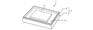
- FIG. 6 is a perspective view showing a configuration example of the surface-mount type crystal resonator 1.
- the crystal resonator 1 is formed by disposing a crystal chip 3 in a thin box-shaped hollow member 2.
- the hollow member 2 includes a hollow main body 4 having an opening 41 and a lid 5 that closes the opening 41 of the main body 4.
- the crystal chip 3 is placed in the main body 4 using a conductive adhesive or the like. After the horizontal mounting, the crystal unit 1 is formed by closing the opening 41 of the main body 4 with the lid 5.
- the main body 4 and the lid 5 are both made of ceramics.
- the main body 4 is mainly formed of ceramics, but the lid 5 is not limited to ceramics and may be formed of other materials such as metal.
- the inventor of the present application applies the above-described crystal resonator to a membrane filtration device used to obtain purified permeated water (permeate) by filtering raw water (raw solution) such as drainage and seawater, Considered wireless communication.
- a sensor for detecting the properties of raw water and permeate filled in the pressure-resistant container in the pressure-resistant container of the membrane filtration device formed by housing the membrane element in the pressure-resistant container and the sensor It is conceivable to provide a wireless communication device that wirelessly transmits this signal to the outside of the pressure vessel, and to apply a crystal resonator to the wireless communication device.
- the pressure resistance of the quartz crystal resonator becomes a problem because the raw water is filled in the pressure vessel at a high pressure of 10 MPa at the maximum. That is, since the crystal resonator has a space for disposing a crystal chip in the hollow member, the pressure resistance is particularly low, and a device for improving the pressure resistance of the crystal resonator is required.
- the present invention has been made in view of the above circumstances, and an object of the present invention is to provide a small and highly pressure-resistant electronic device including a crystal resonator and a membrane filtration apparatus including the electronic device. It is another object of the present invention to provide a low-cost and high pressure resistance electronic device including a crystal resonator and a membrane filtration apparatus including the electronic device.
- An electronic device includes a crystal resonator formed by disposing a crystal chip in a hollow member at least partially made of ceramics, and a circuit board that holds the crystal resonator, A configuration in which the crystal resonator and the circuit board are embedded with a resin can be used.
- the pressure resistance can be improved with a simple configuration in which at least a part of the hollow member of the crystal resonator is formed of ceramics, and the crystal resonator and the circuit board are embedded in the resin. it can.
- the crystal resonator formed by arranging the crystal chip in the hollow member has a particularly low pressure resistance because a space is formed inside, but according to the experimental results conducted by the inventor of the present application, It has been found that the pressure resistance is greatly improved by adopting such a configuration.
- the hollow member of the crystal unit is formed of ceramics, and the crystal unit and the circuit board are embedded in the resin so that the electronic device is accommodated in the case with high pressure resistance.
- an electronic device with high pressure resistance can be provided with a small size and low cost.
- a wireless communication module that is held on the circuit board and performs wireless communication based on an oscillation frequency of the crystal resonator is provided, and the wireless communication module is embedded in a resin.
- wireless communication can be performed by embedding not only the crystal resonator and the circuit board but also the wireless communication module that performs wireless communication based on the oscillation frequency of the crystal resonator with the resin.
- An electronic device with high pressure resistance can be provided in a small size and at low cost.
- the hollow member includes a hollow main body attached to the circuit board and having an opening, and a lid that closes the opening of the main body, and the lid is made of ceramics. Is preferred.
- the portion of the lid that is relatively susceptible to the pressure is formed of ceramics, and the outside of the lid is covered with the resin, so that the pressure resistance can be effectively improved.
- the resin is preferably molded so that the Young's modulus is 0.3 GPa or more and the thickness is 2 mm or more.
- the minimum thickness can be suppressed to 2 mm, thereby providing a smaller and higher pressure resistant electronic device. can do.
- the membrane filtration device includes a membrane element that generates a permeate by filtering a stock solution with a filtration membrane, and a pressure vessel that contains the membrane element and is filled with the stock solution, The structure by which the electronic device was provided in the said pressure vessel is mentioned.
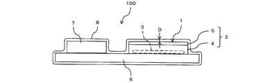
- FIG. 1 is a schematic side view showing an example of an electronic device 100 according to an embodiment of the present invention.
- the electronic device 100 is a wireless communication apparatus that includes the crystal resonator 1 as a timing device and performs wireless communication using the crystal resonator 1.
- the present invention is not limited to the wireless communication apparatus, and can be applied to various electronic devices including the crystal unit 1.
- the electronic device 100 shown in FIG. 1 includes a circuit board 6, and a surface-mounted crystal resonator 1 is held on the mounting surface of the circuit board 6.
- the circuit board 6 is made of, for example, a glass epoxy board.
- the oscillation frequency of the crystal unit 1 may be 8 MHz or 16 MHz, for example.
- a configuration in which a plurality of crystal resonators 1 having different oscillation frequencies are held on the circuit board 6 may be employed.
- the crystal resonator 1 is formed by disposing a crystal chip 3 in a thin box-shaped hollow member 2.
- the hollow member 2 includes a hollow main body 4 having an opening 41 and a lid 5 that closes the opening 41 of the main body 4, and the main body 4 is attached to the mounting surface of the circuit board 6. After the crystal chip 3 is mounted horizontally in the main body 4 using a conductive adhesive or the like, the opening 41 of the main body 4 is closed with a flat lid 5 to form the crystal resonator 1.
- the hollow member 2 is at least partly formed of ceramics.
- the main body 4 and the lid 5 are both ceramic packages formed of ceramics.
- a configuration in which only one of the main body 4 and the lid 5 is formed of ceramics by using another material such as metal for a part of the hollow member 2 may be adopted.
- a wireless communication module 7 that is electrically connected to the crystal resonator 1 and performs wireless communication based on the oscillation frequency of the crystal resonator 1 is mounted.
- the oscillation frequency of the crystal unit 1 is used as a clock frequency, and data is transmitted or received wirelessly at a transmission rate corresponding to the clock frequency.
- the frequency band of the radio wave transmitted and received by the wireless communication module 7 may be 13.56 MHz or 2.4 GHz, for example.
- the circuit board 6 includes a resistor, a capacitor, an inductor, an arithmetic element (CPU, MPU, etc.), a control microcomputer, a rectifier element, an antenna, a memory, and an operational amplifier.
- a signal conversion element analog / digital converter, digital / analog converter, etc.
- an imaging element CCD, CMOS, etc.
- the outer surface of the electronic device 100 is formed of the resin 8 by integrally embedding the circuit board 6 and various electric components mounted on the circuit board 6 with the resin 8. ing.
- the crystal resonator 1, the circuit board 6, and the wireless communication module 7 are all embedded in the resin 8.
- “embedding” means covering the object closely, and is highly waterproof, and there is no space between the object and there is a space between the object. Compared to the case, the pressure resistance against external pressure is high.
- Examples of the molding method of the resin 8 include injection molding, extrusion molding, insert molding, casting molding, vacuum casting molding, and the like, but are not limited to these molding methods.
- Examples of the resin 8 used in insert molding include polystyrene (PS), acrylonitrile-butadiene-styrene copolymer synthetic resin (ABS), polymethyl methacrylate (PMMA), polycarbonate (PC), vinyl chloride resin (PVC), and nylon.
- PA polyacetal
- PET polyethylene terephthalate
- PBT polybutylene terephthalate
- PPO polyphenylene oxide
- PSU polysulfone
- PPS polyphenylene sulfide
- PAS polyallylsulfone
- PAR polyarylate
- PPE polyphenylene ether
- PES polyethersulfone
- PEEK polyetheretherketone
- PI polyimide
- the hollow member 2 of the crystal unit 1 is formed of ceramics, and the pressure resistance is improved with a simple configuration in which the crystal unit 1 and the circuit board 6 are embedded with resin. Can do.
- the crystal resonator 1 formed by arranging the crystal chip 3 in the hollow member 2 has a particularly low pressure resistance because a space is formed inside, but according to the results of experiments conducted by the present inventor. It has been found that the pressure resistance is greatly improved by adopting the above configuration. The experimental results will be described below using Table 1.
- Example 1 A surface-mounted crystal resonator 1, a radio communication module 7 having a frequency band of 2.4 GHz, a capacitor, a resistor, a control microcomputer, a rectifying element, and the like are mounted on a circuit board 6 and embedded entirely in a resin 8. Thus, the electronic device 100 was formed.
- the oscillation frequency of the crystal unit 1 was 8 MHz.
- the hollow member 2 of the crystal unit 1 including the lid 5 is entirely formed of ceramics.
- the electronic device 100 formed as described above was charged for 100 hours under a water pressure of 10 MPa, and then the operation was confirmed and the external shape change of the crystal unit 1 alone was observed. As a result, as shown in Table 1, no change in the outer shape of the crystal unit 1 was confirmed, and normal radio communication could be performed.
- Example 1 The experiment was performed under the same conditions as in Example 1 except that the lid 5 of the hollow member 2 of the crystal resonator 1 was made of metal. That is, as in Example 1, the Young's modulus of the resin 8 is 0.45 MPa, and the thickness D from the upper surface of the crystal unit 1 is 7 mm. As a result of this experiment, as shown in Table 1, a recess was confirmed at the center of the lid 5, and the thickness of the hollow member 2 was reduced by about 0.2 mm. Further, as a result of the operation confirmation, it was not possible to perform wireless communication normally.
- Comparative Example 2 The experiment was performed under the same conditions as in Comparative Example 1 except that the thickness D of the resin 8 was 20 mm. That is, as in Comparative Example 1, the lid 5 of the hollow member 2 of the crystal unit 1 is made of metal, and the Young's modulus of the resin 8 is 0.45 MPa. As a result of this experiment, as shown in Table 1, a recess was confirmed at the center of the lid 5, and the thickness of the hollow member 2 was reduced by about 0.2 mm. Further, as a result of the operation confirmation, it was not possible to perform wireless communication normally. From the comparison between the comparative example 2 and the comparative example 1, it can be seen that if the thickness D of the resin 8 is large to some extent, the pressure resistance is not improved even if it is further increased.
- Comparative Example 3 The experiment was performed under the same conditions as in Comparative Example 1 except that the resin 8 was an epoxy resin with a Young's modulus of 5 GPa and the thickness D was 6 mm. That is, as in Comparative Example 1, the lid 5 of the hollow member 2 of the crystal resonator 1 is made of metal. As a result of this experiment, as shown in Table 1, a decrease in the thickness of the entire hollow member 2 was confirmed, and the thickness of the hollow member 2 was reduced by about 0.2 mm. Further, as a result of the operation confirmation, it was not possible to perform wireless communication normally.
- the resin 8 was an epoxy resin with a Young's modulus of 5 GPa and the thickness D was 6 mm. That is, as in Comparative Example 1, the lid 5 of the hollow member 2 of the crystal resonator 1 is made of metal.
- Table 1 As a result of this experiment, as shown in Table 1, a decrease in the thickness of the entire hollow member 2 was confirmed, and the thickness of the hollow member 2 was reduced by about 0.2 mm
- Comparative Example 4 An experiment was performed under the same conditions as in Comparative Example 3 except that the thickness D of the resin 8 was 25 mm. That is, as in Comparative Example 3, the lid 5 of the hollow member 2 of the crystal unit 1 is made of metal, and the Young's modulus of the resin 8 is 5 GPa. As a result of this experiment, as shown in Table 1, although not visually confirmed, the thickness of the hollow member 2 was reduced by about 0.2 mm. Further, as a result of the operation confirmation, it was not possible to perform wireless communication normally. From a comparison between Comparative Example 4 and Comparative Example 3, it can be seen that if the thickness D of the resin 8 is large to some extent, the pressure resistance is not improved even if it is increased further.
- the hollow member 2 of the crystal resonator 1 (in this example, the lid 5) is formed of ceramics, and the crystal resonator 1 and the circuit board 6 are embedded with the resin 8.
- the resin 8 may have a configuration in which two or more layers are laminated.
- the surface-mounted crystal resonator 1 As in the present embodiment, an opening 41 is formed on the surface of the main body 4 of the hollow member 2 having the largest area, and the opening 41 is covered by the lid 5.
- the lid 5 In the broken configuration, the lid 5 is easily affected by pressure. Therefore, the portion of the lid 5 that is relatively susceptible to the pressure is formed of ceramics, and the outer side of the lid 5 is covered with the resin 8, whereby the pressure resistance can be effectively improved.
- the area of the lid 5 of the hollow member 2 (the surface having the largest area in the main body 4 of the hollow member 2) is generally 90 mm 2 or less (for example, 12.8 mm ⁇ 7.0 mm), and such an area range. If so, even under a pressure environment of a maximum of 10 MPa, the pressure resistance can be satisfactorily exhibited by adopting the configuration as in the present embodiment.
- the crystal resonator 1 and the circuit board 6 not only the crystal resonator 1 and the circuit board 6 but also the wireless communication module 7 that performs wireless communication based on the oscillation frequency of the crystal resonator 1 is embedded in the resin 8 so as to be wireless.
- the electronic device 100 with high pressure resistance that can perform communication can be provided in a small size and at low cost.
- the resin 8 is preferably molded so that the Young's modulus is 0.3 GPa or more and the thickness D is 2 mm or more. As described above, since the minimum thickness D can be suppressed to 2 mm by using the resin 8 having a relatively high rigidity with a Young's modulus of 0.3 GPa or more, it is possible to provide a smaller and higher pressure resistant electronic device. Can do.
- the Young's modulus of the resin 8 is more preferably 2 GPa or more, and further preferably 3 GPa or more.
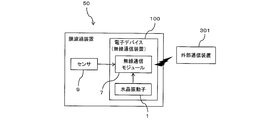
- FIG. 2 is a block diagram illustrating an example of a membrane filtration device 50 including the electronic device 100 of FIG.
- the membrane filtration apparatus 50 is provided with one or a plurality of sensors 9 in addition to the electronic device 100 including the crystal resonator 1 and the wireless communication module 7 as described above.
- the sensor 9 may be mounted on the circuit board 6 or may be provided separately from the circuit board 6.
- the sensor 9 detects the property of the liquid in the membrane filtration device 50, and examples thereof include a conductivity sensor, a flow rate sensor, and a pressure sensor. However, if the sensor 9 detects the property of the liquid, various sensors such as a known physical sensor, chemical sensor, and smart sensor (sensor with information processing function) can be employed depending on the characteristics. Examples of the properties of the liquid detected by the sensor 9 include a flow rate, pressure, conductivity, temperature, and contamination status (ion concentration, etc.).
- the wireless communication module 7 can perform wireless communication with the external communication device 301, and can transmit a signal from the sensor 9 to the external communication device 301 wirelessly. Therefore, by transmitting the data related to the properties of the liquid detected by the sensor 9 from the wireless communication module 7 to the external communication device 301, the properties of the liquid are monitored outside the membrane filtration device 50, and the membrane filtration is performed according to the monitoring result. Maintenance of the apparatus 50 can be performed.
- the membrane filtration apparatus 50 including the above-described electronic device 100 will be described. However, if the configuration is such that the electronic device 100 is provided in a pressure-resistant container that houses the membrane element, the following description will be given.
- the electronic device 100 can be applied to a membrane filtration apparatus having other various configurations.
- FIG. 3 is a schematic cross-sectional view showing an example of the membrane filtration device 50.
- FIG. 4 is a perspective view showing a part of the internal configuration of the membrane element 10 of FIG.
- the membrane filtration device 50 is configured by arranging a plurality of membrane elements 10 in a straight line in the pressure vessel 40.
- the pressure vessel 40 is a resin cylinder called a vessel, and is formed of, for example, FRP (Fiberglass Reinforced Plastics).
- FRP Fiberberglass Reinforced Plastics
- the pressure vessel 40 is formed in a cylindrical shape.
- a raw water inlet 48 into which raw water (raw solution) such as drainage and seawater flows is formed at one end of the pressure vessel 40, and the raw water flowing in from the raw water inlet 48 is filtered by the plurality of membrane elements 10. As a result, purified permeated water (permeated liquid) and concentrated water (concentrated liquid) that is raw water after filtration are obtained.
- a permeate outlet 46 through which permeate flows out and a concentrated water outlet 44 through which concentrated water flows out are formed.
- the membrane element 10 is spirally wound around the central tube 20 in a state where the filtration membrane 12, the supply-side channel material 18, and the permeation-side channel material 14 are laminated.
- RO Reverse Osmosis
- Filtration membranes 12 having the same rectangular shape are superposed on both sides of a rectangular permeation-side flow path material 14 made of a resin-made net-like member, and the three sides are bonded to each other so that an opening is formed on one side.
- a bag-like film member 16 having the above is formed. And the opening part of this membrane member 16 is attached to the outer peripheral surface of the center pipe
- the filtration membrane 12 is formed, for example, by sequentially laminating a porous support and a skin layer (dense layer) on a nonwoven fabric layer.
- the raw water passes through the membrane element 10 through the raw water flow path formed by the supply-side flow path material 18 that functions as a raw water spacer. To do. At that time, the raw water is filtered by the filtration membrane 12, and the permeated water filtered from the raw water penetrates into the permeated water flow path formed by the permeate side flow path material 14 functioning as a permeated water spacer.
- the permeated water that has permeated into the permeated water flow path flows to the central tube 20 side through the permeated water flow path, and the central tube is formed from a plurality of water passage holes (not shown) formed on the outer peripheral surface of the central tube 20. 20 is led.
- the permeated water flows out from the other end side of the membrane element 10 through the central tube 20, and the concentrated water flows out through the raw water flow path formed by the supply side flow path material 18.
- the central tubes 20 of the adjacent membrane elements 10 are connected by a tubular interconnector (connecting portion) 42. Therefore, the raw water flowing in from the raw water inlet 48 flows into the raw water flow path in order from the membrane element 10 on the raw water inlet 48 side, and the permeated water filtered from the raw water in each membrane element 10 is connected by the interconnector 42.
- the permeated water outlet 46 flows out through the single central pipe 20.
- the concentrated water that is filtered and concentrated by passing through the raw water flow path of each membrane element 10 flows out from the concentrated water outlet 44.
- end members 200 are provided at both ends of the membrane element 10. These end members 200 are attached so as to face both ends of the wound membrane member 16 in the axial direction. Thereby, each end member 200 functions as a telescope prevention member for preventing the wound membrane member 16 from becoming a telescope shape by being displaced in the axial direction.
- the end member 200 has a shape in which the outer peripheral surface thereof corresponds to the outer peripheral surface of the membrane element 10, and the outer peripheral surface of the end member 200 is opposed to the inner peripheral surface of the pressure vessel 40. Yes.
- the end member 200 is detachably provided at both ends of each membrane element 10, and the above-described electronic device 100 is provided on the end member 200.
- the sensor 9 may be provided on the end member 200 or may be provided on another member such as the central tube 20 or the membrane member 16.
- a sensor for detecting the property of the permeated water or the raw water in the pressure vessel 40 can be provided.
- the conductivity sensor for detecting the conductivity of the permeated water, the flow rate sensor for detecting the flow rate of the permeated water, the raw water Examples include a pressure sensor that detects pressure.
- An external unit 300 is provided at a position facing the end member 200 outside the pressure vessel 40.
- the external unit 300 is provided with the external communication device 301 described above, and can perform wireless communication with the wireless communication module 7 of the electronic device 100 provided in the end member 200.
- the external unit 300 may be formed integrally with the pressure vessel 40 or may be provided separately from the pressure vessel 40.
- the pressure resistant container 40 is filled with raw water at a high pressure of 10 Mpa at the maximum, so that the pressure resistance of the crystal unit 1 becomes a problem, and the arrangement space of the electronic device 100 is Although there is a problem that it is difficult to secure a large space in the pressure vessel 40, these problems can be solved by using the small electronic device 100 having a high pressure resistance as in this embodiment.
- FIG. 5 is a schematic sectional view showing another example of the membrane filtration device 50. Similar to the membrane filtration device 50 shown in FIG. 3, the membrane filtration device 50 is configured by arranging a plurality of membrane elements 10 in a pressure vessel 40 in a straight line. The specific configuration of the membrane element 10 is the same as the configuration described with reference to FIG.
- an internal unit 400 that is separate from the membrane element 10 is provided.
- the outer surface of the internal unit 400 has a shape corresponding to the outer peripheral surface of the membrane element 10, and the outer peripheral surface of the internal unit 400 is opposed to the inner peripheral surface of the pressure vessel 40.
- the internal unit 400 is attached to the interconnector 42, and the above-described electronic device 100 is provided in the internal unit 400.
- the interconnector 42 can be attached to and detached from the central tube 20 of each membrane element 10, thereby enabling the internal unit 400 to be attached and detached.
- the sensor 9 may be provided in the internal unit 400, or may be provided in another member such as the membrane element 10 or the interconnector 42.
- a sensor for detecting the property of the permeated water or the raw water in the pressure vessel 40 can be provided.
- the conductivity sensor for detecting the conductivity of the permeated water, the flow rate sensor for detecting the flow rate of the permeated water, the raw water Examples include a pressure sensor that detects pressure.
- An external unit 500 is provided at a position facing the internal unit 400 outside the pressure vessel 40.
- the external unit 500 includes the external communication device 301 described above, and can perform wireless communication with the wireless communication module 7 of the electronic device 100 provided in the internal unit 400.
- the external unit 500 may be formed integrally with the pressure vessel 40 or may be provided separately from the pressure vessel 40.
- the pressure vessel 40 is filled with raw water at a high pressure of 10 Mpa at the maximum.
- the pressure resistant container 40 is used as in this embodiment. Therefore, those problems can be solved.
Landscapes
- Engineering & Computer Science (AREA)
- Water Supply & Treatment (AREA)
- Chemical & Material Sciences (AREA)
- Chemical Kinetics & Catalysis (AREA)
- Organic Chemistry (AREA)
- Environmental & Geological Engineering (AREA)
- Life Sciences & Earth Sciences (AREA)
- Hydrology & Water Resources (AREA)
- Nanotechnology (AREA)
- Manufacturing & Machinery (AREA)
- Microelectronics & Electronic Packaging (AREA)
- Separation Using Semi-Permeable Membranes (AREA)
- Non-Metallic Protective Coatings For Printed Circuits (AREA)
- Oscillators With Electromechanical Resonators (AREA)
- Piezo-Electric Or Mechanical Vibrators, Or Delay Or Filter Circuits (AREA)
Abstract
水晶振動子を備えた小型で耐圧性の高い電子デバイス及びこれを備えた膜濾過装置を提供する。水晶振動子1の中空部材2の少なくとも一部をセラミックスで形成するとともに、水晶振動子1及び回路基板6を樹脂により包埋する。中空部材2内に水晶チップ3が配置されることにより形成された水晶振動子1は、内部に空間が形成されているため特に耐圧性が低いが、水晶振動子1の中空部材2の少なくとも一部をセラミックスで形成するとともに、水晶振動子1及び回路基板6を樹脂8により包埋するといった構成により、小型で耐圧性の高い電子デバイス100を提供することができる。
Description
本発明は、水晶振動子を備えた電子デバイス及びこれを備えた膜濾過装置に関するものである。
従来から、水晶振動子を用いて無線通信を行う電子デバイスが知られている(例えば、特許文献1)。この水晶振動子には、リード型や表面実装型のものがあり、それぞれ中空部材内に水晶チップが配置されることにより形成されている。
図6は、表面実装型の水晶振動子1の一構成例を示した斜視図である。この水晶振動子1は、薄い箱状の中空部材2内に水晶チップ3が配置されることにより形成されている。中空部材2には、開口部41を有する中空状の本体4と、この本体4の開口部41を塞ぐ蓋5が備えられ、本体4内に、導電性接着剤などを用いて水晶チップ3を水平にマウントした後、本体4の開口部41を蓋5で塞ぐことにより、水晶振動子1が形成される。
この例では、本体4及び蓋5がいずれもセラミックスにより形成されている。本体4は、セラミックスにより形成するのが主流であるが、蓋5は、セラミックスに限らず、金属などの他の材料で形成される場合がある。
本願発明者は、排水や海水などの原水(原液)を濾過して、浄化された透過水(透過液)を得るために用いられる膜濾過装置に、上記のような水晶振動子を適用し、無線通信を行うことを考えた。例えば、耐圧容器内に膜エレメントを収容することにより形成された膜濾過装置の耐圧容器内に、当該耐圧容器内に充填される原水や透過水の性状を検知するためのセンサと、当該センサからの信号を耐圧容器の外部に無線で送信する無線通信装置とを設け、当該無線通信装置に水晶振動子を適用することが考えられる。
しかしながら、上記のような膜濾過装置では、耐圧容器内に最大10MPaといった高い圧力で原水が充填されるため、水晶振動子の耐圧性が問題となる。すなわち、水晶振動子は、中空部材内に水晶チップを配置するための空間が形成されているため特に耐圧性が低く、水晶振動子の耐圧性を向上するための工夫が必要となる。
高圧環境下である耐圧容器内に水晶振動子を設けるという着想自体、一般的に考えられるものではないが、仮にそのような構成を採用する場合には、水晶振動子が実装された電子デバイス全体を耐圧性の高いケース内に収容する構成に想到するのが通常と考えられる。しかしながら、電子デバイス全体をケース内に収容することにより形成された部品は、比較的大型となり、その分大きな配置スペースを耐圧容器内に確保する必要がある。
上記のように電子デバイス全体をケース内に収容した部品を耐圧容器内に配置するために、膜エレメントを小型化したり、耐圧容器を大型化したりすることも考えられるが、膜エレメントや耐圧容器などの部材は、既にモジュール化され、システム全体としての造水コストを低減しているため、規格の変更によってシステム全体のコストを増大させることになり好ましくない。また、膜エレメントを小型化することに関しては、1本当たりの膜エレメントからの造水量が減少するため、生産性を考慮すると好ましくない。また、造水システムに多数用いられる上記電子デバイスをそれぞれケース内に収容すると、コストが高くなるといった問題もある。
以上のような課題は、膜濾過装置に限らず、水晶振動子を備えた電子デバイスを高圧環境下で使用する場合には、他の装置においても生じる課題である。
本発明は、上記実情に鑑みてなされたものであり、水晶振動子を備えた小型で耐圧性の高い電子デバイス及びこれを備えた膜濾過装置を提供することを目的とする。また、本発明は、水晶振動子を備えた低コストで耐圧性の高い電子デバイス及びこれを備えた膜濾過装置を提供することを目的とする。
本発明に係る電子デバイスとしては、少なくとも一部がセラミックスからなる中空部材内に水晶チップが配置されることにより形成された水晶振動子と、前記水晶振動子を保持する回路基板とを備え、前記水晶振動子及び前記回路基板が樹脂により包埋された構成が挙げられる。
このような構成によれば、水晶振動子の中空部材の少なくとも一部をセラミックスで形成するとともに、水晶振動子及び回路基板を樹脂により包埋するといった簡単な構成で、耐圧性を向上することができる。中空部材内に水晶チップが配置されることにより形成された水晶振動子は、内部に空間が形成されているため特に耐圧性が低いが、本願発明者が行った実験結果によれば、上記のような構成を採用することにより耐圧性が大幅に向上することが分かった。
このように、水晶振動子の中空部材の少なくとも一部をセラミックスで形成するとともに、水晶振動子及び回路基板を樹脂により包埋するといった構成により、耐圧性の高いケース内に電子デバイスを収容するような構成と比較して、小型かつ低コストで、耐圧性の高い電子デバイスを提供することができる。
本発明において、前記回路基板に保持され、前記水晶振動子の発振周波数に基づいて無線通信を行う無線通信モジュールを備え、前記無線通信モジュールが樹脂により包埋されていることが好ましい。
このような構成によれば、水晶振動子及び回路基板だけでなく、水晶振動子の発振周波数に基づいて無線通信を行う無線通信モジュールも樹脂で包埋することにより、無線通信を行うことができる耐圧性の高い電子デバイスを小型かつ低コストで提供することができる。
本発明において、前記中空部材には、前記回路基板に取り付けられ、開口部を有する中空状の本体と、当該本体の開口部を塞ぐ蓋とが備えられ、前記蓋がセラミックスにより形成されていることが好ましい。
このような構成によれば、圧力の影響を比較的受けやすい蓋の部分がセラミックスにより形成され、その蓋の外側が樹脂で覆われることにより、耐圧性を効果的に向上することができる。
本発明において、前記樹脂は、ヤング率が0.3GPa以上であり、厚みが2mm以上になるように成形されていることが好ましい。
このような構成によれば、ヤング率が0.3GPa以上の剛性が比較的高い樹脂を用いることにより、最低厚みを2mmにまで抑えることができるので、より小型で耐圧性の高い電子デバイスを提供することができる。
本発明に係る膜濾過装置としては、濾過膜で原液を濾過することにより透過液を生成する膜エレメントと、前記膜エレメントを収容し、その内部に原液が充填される耐圧容器とを備え、前記電子デバイスが前記耐圧容器内に設けられた構成が挙げられる。
図1は、本発明の一実施形態に係る電子デバイス100の一例を示す概略側面図である。この電子デバイス100は、水晶振動子1をタイミングデバイスとして備え、当該水晶振動子1を用いて無線通信を行う無線通信装置である。ただし、本発明は、無線通信装置に限らず、水晶振動子1を備えた各種電子デバイスに採用することができる。
図1に示した電子デバイス100には、回路基板6が備えられており、当該回路基板6の実装面上に表面実装型の水晶振動子1が保持されている。回路基板6は、例えばガラスエポキシ基板からなる。水晶振動子1の発振周波数は、例えば8MHz又は16MHzなどであってもよい。また、発振周波数の異なる複数の水晶振動子1が回路基板6に保持された構成であってもよい。
水晶振動子1は、図6を用いて既に説明した通り、薄い箱状の中空部材2内に水晶チップ3が配置されることにより形成されている。中空部材2には、開口部41を有する中空状の本体4と、この本体4の開口部41を塞ぐ蓋5が備えられ、本体4が回路基板6の実装面に取り付けられている。本体4内に、導電性接着剤などを用いて水晶チップ3を水平にマウントした後、本体4の開口部41を平板状の蓋5で塞ぐことにより、水晶振動子1が形成される。
中空部材2は、その少なくとも一部がセラミックスにより形成されており、この例では、本体4及び蓋5がいずれもセラミックスにより形成されたセラミックスパッケージである。ただし、中空部材2の一部に金属などの他の材料が用いられることにより、本体4又は蓋5のいずれか一方のみがセラミックスにより形成された構成であってもよい。
回路基板6には、水晶振動子1に対して電気的に接続され、水晶振動子1の発振周波数に基づいて無線通信を行う無線通信モジュール7が実装されている。具体的には、水晶振動子1の発振周波数をクロック周波数として、そのクロック周波数に応じた伝送速度でデータが無線で送信又は受信されるようになっている。この無線通信モジュール7により送受信される電波の周波数帯は、例えば13.56MHz又は2.4GHzなどであってもよい。
回路基板6には、上記水晶振動子1及び無線通信モジュール7の他にも、図示しない抵抗、コンデンサ、インダクタ、演算素子(CPU、MPUなど)、制御用マイコン、整流素子、アンテナ、メモリ、オペアンプ、信号変換素子(アナログデジタルコンバータ、デジタルアナログコンバータなど)、イメージング素子(CCD、CMOSなど)が実装され、互いに電気的に接続されている。
本実施形態では、回路基板6と、当該回路基板6に実装されている各種電気部品とが、樹脂8で一体的に包埋されることにより、電子デバイス100の外表面が樹脂8により形成されている。これにより、水晶振動子1、回路基板6及び無線通信モジュール7は、いずれも樹脂8により包埋された状態となっている。ここで、「包埋」とは、対象物を密着して覆うことを意味しており、防水性が高い上、対象物との間に空間がないため、対象物との間に空間がある場合と比べて外部からの圧力に対する耐圧性が高い。
樹脂8の成形方法としては、例えば射出成形、押出成形、インサート成形、注型成形、真空注型成形などを挙げることができるが、これらの成形方法に限られるものではない。インサート成形などで使用される樹脂8としては、ポリスチレン(PS)、アクリロニトリル-ブタジエン-スチレン共重合合成樹脂(ABS)、ポリメチルメタクリレート(PMMA)、ポリカーボネート(PC)、塩化ビニル樹脂(PVC)、ナイロン6(PA)、ポリアセタール(POM)、ポリエチレンテレフタレート(PET)、ポリブチレンテレフタレート(PBT)、ポリフェニレンオキサイド(PPO)、ポリサルホン(PSU)、ポリフェニレンサルファイド(PPS)、ポリアリルサルフォン(PAS)、ポリアリレート(PAR)、ポリフェニレンエーテル(PPE)、ポリエーテルサルホン(PES)ポリエーテルエーテルケトン(PEEK)、ポリイミド(PI)などが挙げられる。注型成形で使用される樹脂8としては、エポキシ樹脂やウレタン樹脂などが挙げられる。また、上記のような樹脂8にガラス繊維や炭素繊維、充填剤などの添加物を添加することにより、強度を向上させてもよい。
本実施形態では、水晶振動子1の中空部材2の少なくとも一部をセラミックスで形成するとともに、水晶振動子1及び回路基板6を樹脂により包埋するといった簡単な構成で、耐圧性を向上することができる。中空部材2内に水晶チップ3が配置されることにより形成された水晶振動子1は、内部に空間が形成されているため特に耐圧性が低いが、本願発明者が行った実験結果によれば、上記のような構成を採用することにより耐圧性が大幅に向上することが分かった。以下、その実験結果を表1を用いて説明する。
(実施例1)
回路基板6上に、表面実装型の水晶振動子1、周波数帯が2.4GHzの無線通信モジュール7、コンデンサ、抵抗、制御用マイコン、整流素子などを実装し、全体を樹脂8で包埋することにより電子デバイス100を形成した。水晶振動子1の発振周波数は、8MHzとした。水晶振動子1の中空部材2は、蓋5も含めて全体をセラミックスにより形成した。樹脂8としては、ヤング率が0.45MPaのウレタン樹脂を用い、水晶振動子1の上面(蓋5の上面)からの厚みDが7mmとなるように成形した。
回路基板6上に、表面実装型の水晶振動子1、周波数帯が2.4GHzの無線通信モジュール7、コンデンサ、抵抗、制御用マイコン、整流素子などを実装し、全体を樹脂8で包埋することにより電子デバイス100を形成した。水晶振動子1の発振周波数は、8MHzとした。水晶振動子1の中空部材2は、蓋5も含めて全体をセラミックスにより形成した。樹脂8としては、ヤング率が0.45MPaのウレタン樹脂を用い、水晶振動子1の上面(蓋5の上面)からの厚みDが7mmとなるように成形した。
上記のようにして形成された電子デバイス100を10MPaの水圧下に100時間投入した後、その動作確認、及び、水晶振動子1単体の外形変化の観察を行った。その結果、表1に示すように、水晶振動子1に外形変化は確認されず、正常に無線通信を行うことができた。
(比較例1)
水晶振動子1の中空部材2の蓋5を金属で形成した以外は、実施例1と同様の条件で実験を行った。すなわち、実施例1と同様、樹脂8のヤング率は0.45MPaであり、水晶振動子1の上面からの厚みDは7mmである。この実験の結果、表1に示すように、蓋5の中央部には凹みが確認され、中空部材2の厚みが0.2mm程度減少した。また、動作確認の結果、正常に無線通信を行うことはできなかった。
水晶振動子1の中空部材2の蓋5を金属で形成した以外は、実施例1と同様の条件で実験を行った。すなわち、実施例1と同様、樹脂8のヤング率は0.45MPaであり、水晶振動子1の上面からの厚みDは7mmである。この実験の結果、表1に示すように、蓋5の中央部には凹みが確認され、中空部材2の厚みが0.2mm程度減少した。また、動作確認の結果、正常に無線通信を行うことはできなかった。
(比較例2)
樹脂8の厚みDを20mmとした以外は、比較例1と同様の条件で実験を行った。すなわち、比較例1と同様、水晶振動子1の中空部材2の蓋5は金属製であり、樹脂8のヤング率は0.45MPaである。この実験の結果、表1に示すように、蓋5の中央部には凹みが確認され、中空部材2の厚みが0.2mm程度減少した。また、動作確認の結果、正常に無線通信を行うことはできなかった。この比較例2と比較例1との比較から、樹脂8の厚みDがある程度大きければ、それ以上大きくしても耐圧性は向上しないことが分かる。
樹脂8の厚みDを20mmとした以外は、比較例1と同様の条件で実験を行った。すなわち、比較例1と同様、水晶振動子1の中空部材2の蓋5は金属製であり、樹脂8のヤング率は0.45MPaである。この実験の結果、表1に示すように、蓋5の中央部には凹みが確認され、中空部材2の厚みが0.2mm程度減少した。また、動作確認の結果、正常に無線通信を行うことはできなかった。この比較例2と比較例1との比較から、樹脂8の厚みDがある程度大きければ、それ以上大きくしても耐圧性は向上しないことが分かる。
(比較例3)
樹脂8をヤング率5GPaのエポキシ樹脂とし、その厚みDを6mmとした以外は、比較例1と同様の条件で実験を行った。すなわち、比較例1と同様、水晶振動子1の中空部材2の蓋5は金属製である。この実験の結果、表1に示すように、中空部材2全体の厚みの減少が確認され、当該中空部材2の厚みが0.2mm程度減少した。また、動作確認の結果、正常に無線通信を行うことはできなかった。
樹脂8をヤング率5GPaのエポキシ樹脂とし、その厚みDを6mmとした以外は、比較例1と同様の条件で実験を行った。すなわち、比較例1と同様、水晶振動子1の中空部材2の蓋5は金属製である。この実験の結果、表1に示すように、中空部材2全体の厚みの減少が確認され、当該中空部材2の厚みが0.2mm程度減少した。また、動作確認の結果、正常に無線通信を行うことはできなかった。
(比較例4)
樹脂8の厚みDを25mmとした以外は、比較例3と同様の条件で実験を行った。すなわち、比較例3と同様、水晶振動子1の中空部材2の蓋5は金属製であり、樹脂8のヤング率は5GPaである。この実験の結果、表1に示すように、目視では確認できないものの、中空部材2の厚みが0.2mm程度減少した。また、動作確認の結果、正常に無線通信を行うことはできなかった。この比較例4と比較例3との比較からも、樹脂8の厚みDがある程度大きければ、それ以上大きくしても耐圧性は向上しないことが分かる。
樹脂8の厚みDを25mmとした以外は、比較例3と同様の条件で実験を行った。すなわち、比較例3と同様、水晶振動子1の中空部材2の蓋5は金属製であり、樹脂8のヤング率は5GPaである。この実験の結果、表1に示すように、目視では確認できないものの、中空部材2の厚みが0.2mm程度減少した。また、動作確認の結果、正常に無線通信を行うことはできなかった。この比較例4と比較例3との比較からも、樹脂8の厚みDがある程度大きければ、それ以上大きくしても耐圧性は向上しないことが分かる。
上記実施例1のように、水晶振動子1の中空部材2の少なくとも一部(この例では、蓋5)をセラミックスで形成するとともに、水晶振動子1及び回路基板6を樹脂8により包埋するといった構成により、耐圧性の高いケース内に電子デバイスを収容するような構成と比較して、小型かつ低コストで、耐圧性の高い電子デバイス100を提供することができる。樹脂8は、2層以上積層された構成であってもよい。
特に、中空部材2の本体4における最も面積の大きい面には、より大きな圧力が作用するため、この面をセラミックスで形成することが好ましい。本実施形態のような表面実装型の水晶振動子1に例示されるように、中空部材2の本体4における最も面積の大きい面に開口部41が形成され、その開口部41が蓋5により覆われた構成では、当該蓋5の部分が圧力の影響を受けやすい。したがって、圧力の影響を比較的受けやすい蓋5の部分がセラミックスにより形成され、その蓋5の外側が樹脂8で覆われることにより、耐圧性を効果的に向上することができる。中空部材2の蓋5(中空部材2の本体4における最も面積の大きい面)の面積は、一般的に90mm2以下(例えば、12.8mm×7.0mmなど)であり、このような面積範囲であれば、最大10MPaの圧力環境下においても、本実施形態のような構成を採用することにより耐圧性を良好に発揮することができる。
また、本実施形態のように、水晶振動子1及び回路基板6だけでなく、水晶振動子1の発振周波数に基づいて無線通信を行う無線通信モジュール7も樹脂8で包埋することにより、無線通信を行うことができる耐圧性の高い電子デバイス100を小型かつ低コストで提供することができる。
樹脂8は、ヤング率が0.3GPa以上であり、厚みDが2mm以上になるように成形されていることが好ましい。このように、ヤング率が0.3GPa以上の剛性が比較的高い樹脂8を用いることにより、最低厚みDを2mmにまで抑えることができるので、より小型で耐圧性の高い電子デバイスを提供することができる。なお、樹脂8のヤング率は、2GPa以上であればより好ましく、3GPa以上であればさらに好ましい。
図2は、図1の電子デバイス100を備えた膜濾過装置50の一例を示すブロック図である。膜濾過装置50には、上述のような水晶振動子1及び無線通信モジュール7を備えた電子デバイス100の他に、1つ又は複数のセンサ9が設けられている。センサ9は、回路基板6に実装されていてもよいし、回路基板6とは別個に設けられていてもよい。
センサ9は、膜濾過装置50内の液体の性状を検知するものであり、電導度センサ、流量センサ、圧力センサなどを例示することができる。ただし、液体の性状を検知するセンサ9であれば、その特性に応じて、公知の物理センサ、化学センサ、スマートセンサ(情報処理機能付きセンサ)などの各種センサを採用することができる。センサ9により検知される液体の性状としては、例えば流量、圧力、電導度、温度、汚染状況(イオン濃度など)を挙げることができる。
無線通信モジュール7は、外部通信装置301との間で無線通信を行うことができ、センサ9からの信号を外部通信装置301へ無線で送信することができる。したがって、センサ9により検知した液体の性状に関するデータを無線通信モジュール7から外部通信装置301へ送信することにより、膜濾過装置50の外部で液体の性状を監視し、その監視結果に応じて膜濾過装置50のメンテナンスを行うことができる。
以下では、上述の電子デバイス100を備えた膜濾過装置50の具体的構成について説明するが、膜エレメントを収容する耐圧容器内に電子デバイス100が設けられたような構成であれば、以下に説明するような構成に限られるものではなく、他の各種構成を有する膜濾過装置に電子デバイス100を適用することができる。
図3は、膜濾過装置50の一例を示した概略断面図である。また、図4は、図3の膜エレメント10の内部構成の一部を示した斜視図である。この膜濾過装置50は、膜エレメント10を耐圧容器40内に一直線上に複数配置することにより構成されている。
耐圧容器40は、ベッセルと呼ばれる樹脂製の筒体であり、例えばFRP(Fiberglass Reinforced Plastics)により形成される。この例では、耐圧容器40は、円筒状に形成されている。
耐圧容器40の一端部には、排水や海水などの原水(原液)が流入する原水流入口48が形成されており、当該原水流入口48から流入する原水が複数の膜エレメント10で濾過されることにより、浄化された透過水(透過液)と、濾過後の原水である濃縮水(濃縮液)とが得られる。耐圧容器40の他端部には、透過水が流出する透過水流出口46と、濃縮水が流出する濃縮水流出口44とが形成されている。
図4に示すように、膜エレメント10は、濾過膜12と供給側流路材18と透過側流路材14とが積層された状態で中心管20の周囲にスパイラル状に巻回されることにより形成されたRO(Reverse Osmosis:逆浸透)エレメントである。
樹脂製の網状部材からなる矩形形状の透過側流路材14の両面には、同一の矩形形状からなる濾過膜12が重ね合わせられ、その3辺が接着されることにより、1辺に開口部を有する袋状の膜部材16が形成される。そして、この膜部材16の開口部が中心管20の外周面に取り付けられ、樹脂製の網状部材からなる供給側流路材18とともに中心管20の周囲に巻回されることにより、上記膜エレメント10が形成される。上記濾過膜12は、例えば不織布層上に多孔性支持体及びスキン層(緻密層)が順次に積層されることにより形成される。
上記のようにして形成された膜エレメント10の一端側から原水を供給すると、原水スペーサとして機能する供給側流路材18により形成された原水流路を介して、膜エレメント10内を原水が通過する。その際、原水が濾過膜12により濾過され、原水から濾過された透過水が、透過水スペーサとして機能する透過側流路材14により形成された透過水流路内に浸透する。
その後、透過水流路内に浸透した透過水が、当該透過水流路を通って中心管20側に流れ、中心管20の外周面に形成された複数の通水孔(図示せず)から中心管20内に導かれる。これにより、膜エレメント10の他端側から、中心管20を介して透過水が流出するとともに、供給側流路材18により形成された原水流路を介して濃縮水が流出することとなる。
図3に示すように、耐圧容器40内に収容されている複数の膜エレメント10は、隣接する膜エレメント10の中心管20同士が管状のインターコネクタ(連結部)42で連結されている。したがって、原水流入口48から流入した原水は、当該原水流入口48側の膜エレメント10から順に原水流路内に流れ込み、各膜エレメント10で原水から濾過された透過水が、インターコネクタ42により接続された1本の中心管20を介して透過水流出口46から流出する。一方、各膜エレメント10の原水流路を通過することにより透過水が濾過されて濃縮された濃縮水は、濃縮水流出口44から流出する。
この図3の例では、膜エレメント10の両端部に端部部材200が設けられている。これらの端部部材200は、巻回された膜部材16の軸線方向の両端部に対向するように取り付けられている。これにより、各端部部材200は、巻回された膜部材16が軸線方向にずれることによってテレスコープ状になるのを防止するためのテレスコープ防止部材として機能する。
端部部材200は、その外周面が膜エレメント10の外周面に対応する形状を有しており、当該端部部材200の外周面は、耐圧容器40の内周面に近接して対向している。この例では、端部部材200が各膜エレメント10の両端部に、着脱可能に設けられており、当該端部部材200に上述の電子デバイス100が設けられている。
センサ9は、端部部材200に設けられていてもよいし、中心管20又は膜部材16などの他の部材に設けられていてもよい。センサ9としては、耐圧容器40内の透過水又は原水の性状を検知するセンサを設けることができ、透過水の電導度を検知する電導度センサ、透過水の流量を検知する流量センサ、原水の圧力を検知する圧力センサなどを例示することができる。
耐圧容器40の外部における端部部材200に対向する位置には、外部ユニット300が設けられている。この外部ユニット300には、上述の外部通信装置301が設けられており、端部部材200に設けられている電子デバイス100の無線通信モジュール7との間で無線通信を行うことができる。外部ユニット300は、耐圧容器40と一体的に形成されていてもよいし、耐圧容器40とは別個に設けられていてもよい。
このような構成を有する膜濾過装置50では、耐圧容器40内に最大10Mpaという高い圧力で原水が充填されるため、水晶振動子1の耐圧性が問題になるとともに、電子デバイス100の配置スペースとして耐圧容器40内に大きなスペースを確保することが難しいという問題があるが、本実施形態のように耐圧性の高い小型の電子デバイス100を用いることにより、それらの問題を解消することができる。
図5は、膜濾過装置50の他の例を示した概略断面図である。この膜濾過装置50は、図3に示した膜濾過装置50と同様、膜エレメント10を耐圧容器40内に一直線上に複数配置することにより構成されている。膜エレメント10の具体的構成は、図4を用いて説明した構成と同様である。
この図5の例では、膜エレメント10とは別体である内部ユニット400が設けられている。内部ユニット400は、その外周面が膜エレメント10の外周面に対応する形状を有しており、当該内部ユニット400の外周面は、耐圧容器40の内周面に近接して対向している。この例では、内部ユニット400が、インターコネクタ42に取り付けられており、当該内部ユニット400に上述の電子デバイス100が設けられている。インターコネクタ42は、各膜エレメント10の中心管20に対して着脱可能であり、これにより、内部ユニット400が着脱可能となっている。
センサ9は、内部ユニット400に設けられていてもよいし、膜エレメント10又はインターコネクタ42などの他の部材に設けられていてもよい。センサ9としては、耐圧容器40内の透過水又は原水の性状を検知するセンサを設けることができ、透過水の電導度を検知する電導度センサ、透過水の流量を検知する流量センサ、原水の圧力を検知する圧力センサなどを例示することができる。
耐圧容器40の外部における内部ユニット400に対向する位置には、外部ユニット500が設けられている。この外部ユニット500には、上述の外部通信装置301が設けられており、内部ユニット400に設けられている電子デバイス100の無線通信モジュール7との間で無線通信を行うことができる。外部ユニット500は、耐圧容器40と一体的に形成されていてもよいし、耐圧容器40とは別個に設けられていてもよい。
このような構成を有する膜濾過装置50においても、図3に示した膜濾過装置50と同様に、耐圧容器40内に最大10Mpaという高い圧力で原水が充填されるため、水晶振動子1の耐圧性が問題になるとともに、電子デバイス100の配置スペースとして耐圧容器40内に大きなスペースを確保することが難しいという問題があるが、本実施形態のように耐圧性の高い小型の電子デバイス100を用いることにより、それらの問題を解消することができる。
1 水晶振動子
2 中空部材
3 水晶チップ
4 本体
5 蓋
6 回路基板
7 無線通信モジュール
8 樹脂
9 センサ
10 膜エレメント
40 耐圧容器
50 膜濾過装置
100 電子デバイス
2 中空部材
3 水晶チップ
4 本体
5 蓋
6 回路基板
7 無線通信モジュール
8 樹脂
9 センサ
10 膜エレメント
40 耐圧容器
50 膜濾過装置
100 電子デバイス
Claims (5)
- 少なくとも一部がセラミックスからなる中空部材内に水晶チップが配置されることにより形成された水晶振動子と、
前記水晶振動子を保持する回路基板とを備え、
前記水晶振動子及び前記回路基板が樹脂により包埋されていることを特徴とする電子デバイス。 - 前記回路基板に保持され、前記水晶振動子の発振周波数に基づいて無線通信を行う無線通信モジュールを備え、
前記無線通信モジュールが樹脂により包埋されていることを特徴とする請求項1に記載の電子デバイス。 - 前記中空部材には、前記回路基板に取り付けられ、開口部を有する中空状の本体と、当該本体の開口部を塞ぐ蓋とが備えられ、
前記蓋がセラミックスにより形成されていることを特徴とする請求項1に記載の電子デバイス。 - 前記樹脂は、ヤング率が0.3GPa以上であり、厚みが2mm以上になるように成形されていることを特徴とする請求項1に記載の電子デバイス。
- 濾過膜で原液を濾過することにより透過液を生成する膜エレメントと、
前記膜エレメントを収容し、その内部に原液が充填される耐圧容器とを備え、
請求項1~4のいずれかに記載の電子デバイスが前記耐圧容器内に設けられたことを特徴とする膜濾過装置。
Applications Claiming Priority (2)
| Application Number | Priority Date | Filing Date | Title |
|---|---|---|---|
| JP2009197165A JP5225953B2 (ja) | 2009-08-27 | 2009-08-27 | 電子デバイス及びこれを備えた膜濾過装置 |
| JP2009-197165 | 2009-08-27 |
Publications (1)
| Publication Number | Publication Date |
|---|---|
| WO2011024795A1 true WO2011024795A1 (ja) | 2011-03-03 |
Family
ID=43627899
Family Applications (1)
| Application Number | Title | Priority Date | Filing Date |
|---|---|---|---|
| PCT/JP2010/064260 Ceased WO2011024795A1 (ja) | 2009-08-27 | 2010-08-24 | 電子デバイス及びこれを備えた膜濾過装置 |
Country Status (2)
| Country | Link |
|---|---|
| JP (1) | JP5225953B2 (ja) |
| WO (1) | WO2011024795A1 (ja) |
Families Citing this family (1)
| Publication number | Priority date | Publication date | Assignee | Title |
|---|---|---|---|---|
| CN112954910A (zh) * | 2021-01-28 | 2021-06-11 | 林小华 | 一种电路板膜渣过滤收集装置 |
Citations (4)
| Publication number | Priority date | Publication date | Assignee | Title |
|---|---|---|---|---|
| JP2007036535A (ja) * | 2005-07-26 | 2007-02-08 | Seiko Epson Corp | 圧電デバイスおよび圧電デバイスの製造方法 |
| JP2007082113A (ja) * | 2005-09-16 | 2007-03-29 | Nippon Dempa Kogyo Co Ltd | 無線モジュール素子及びその実装方法 |
| JP2007311416A (ja) * | 2006-05-16 | 2007-11-29 | Fujifilm Corp | 固体撮像装置 |
| WO2009078413A1 (ja) * | 2007-12-17 | 2009-06-25 | Nitto Denko Corporation | スパイラル型膜エレメント及びこれを備えたスパイラル型膜濾過装置 |
Family Cites Families (1)
| Publication number | Priority date | Publication date | Assignee | Title |
|---|---|---|---|---|
| JP2003281985A (ja) * | 2002-03-25 | 2003-10-03 | Nec Schott Components Corp | 中空パッケ−ジおよびその製造方法 |
-
2009
- 2009-08-27 JP JP2009197165A patent/JP5225953B2/ja not_active Expired - Fee Related
-
2010
- 2010-08-24 WO PCT/JP2010/064260 patent/WO2011024795A1/ja not_active Ceased
Patent Citations (4)
| Publication number | Priority date | Publication date | Assignee | Title |
|---|---|---|---|---|
| JP2007036535A (ja) * | 2005-07-26 | 2007-02-08 | Seiko Epson Corp | 圧電デバイスおよび圧電デバイスの製造方法 |
| JP2007082113A (ja) * | 2005-09-16 | 2007-03-29 | Nippon Dempa Kogyo Co Ltd | 無線モジュール素子及びその実装方法 |
| JP2007311416A (ja) * | 2006-05-16 | 2007-11-29 | Fujifilm Corp | 固体撮像装置 |
| WO2009078413A1 (ja) * | 2007-12-17 | 2009-06-25 | Nitto Denko Corporation | スパイラル型膜エレメント及びこれを備えたスパイラル型膜濾過装置 |
Also Published As
| Publication number | Publication date |
|---|---|
| JP5225953B2 (ja) | 2013-07-03 |
| JP2011049878A (ja) | 2011-03-10 |
Similar Documents
| Publication | Publication Date | Title |
|---|---|---|
| JP5473482B2 (ja) | 膜濾過装置 | |
| JP5379464B2 (ja) | スパイラル型膜エレメント及びこれを備えたスパイラル型膜濾過装置 | |
| US8568596B2 (en) | Membrane filtering device managing system and membrane filtering device for use therein, and membrane filtering device managing method | |
| JP5578783B2 (ja) | スパイラル型膜濾過装置及び取付部材、並びに、これを用いた膜濾過装置管理システム及び膜濾過装置管理方法 | |
| CN104528976A (zh) | 一体复合滤芯和具有其的净水系统 | |
| JP2000354742A (ja) | スパイラル型分離膜エレメント | |
| CN103402613B (zh) | 分离膜组件 | |
| JP5687115B2 (ja) | 分離膜モジュールおよび連結部材 | |
| WO2011024801A1 (ja) | 膜濾過装置 | |
| JP5225953B2 (ja) | 電子デバイス及びこれを備えた膜濾過装置 | |
| JP2012143662A (ja) | 膜濾過装置及び膜濾過装置の運転方法 | |
| CN103328077A (zh) | 反渗透处理装置 | |
| WO2012117667A1 (ja) | 連結部材および分離膜モジュール | |
| JP2011045842A (ja) | 膜エレメント及び膜濾過装置 | |
| JP2012176372A (ja) | 連結部材および分離膜モジュール | |
| US20140061111A1 (en) | Encapsulated water filter media assembly | |
| JP4228324B2 (ja) | 流体分離素子 | |
| JP2008221107A (ja) | 液体分離膜モジュール |
Legal Events
| Date | Code | Title | Description |
|---|---|---|---|
| 121 | Ep: the epo has been informed by wipo that ep was designated in this application |
Ref document number: 10811845 Country of ref document: EP Kind code of ref document: A1 |
|
| NENP | Non-entry into the national phase |
Ref country code: DE |
|
| 122 | Ep: pct application non-entry in european phase |
Ref document number: 10811845 Country of ref document: EP Kind code of ref document: A1 |