WO2011021279A1 - 物質の応力を算出する情報処理装置 - Google Patents
物質の応力を算出する情報処理装置 Download PDFInfo
- Publication number
- WO2011021279A1 WO2011021279A1 PCT/JP2009/064470 JP2009064470W WO2011021279A1 WO 2011021279 A1 WO2011021279 A1 WO 2011021279A1 JP 2009064470 W JP2009064470 W JP 2009064470W WO 2011021279 A1 WO2011021279 A1 WO 2011021279A1
- Authority
- WO
- WIPO (PCT)
- Prior art keywords
- atomic
- crystal
- substance
- atoms
- parallelepiped
- Prior art date
- Legal status (The legal status is an assumption and is not a legal conclusion. Google has not performed a legal analysis and makes no representation as to the accuracy of the status listed.)
- Ceased
Links
Images















Classifications
-
- G—PHYSICS
- G16—INFORMATION AND COMMUNICATION TECHNOLOGY [ICT] SPECIALLY ADAPTED FOR SPECIFIC APPLICATION FIELDS
- G16C—COMPUTATIONAL CHEMISTRY; CHEMOINFORMATICS; COMPUTATIONAL MATERIALS SCIENCE
- G16C10/00—Computational theoretical chemistry, i.e. ICT specially adapted for theoretical aspects of quantum chemistry, molecular mechanics, molecular dynamics or the like
Definitions
- the present invention relates to an information processing apparatus for calculating a stress of a substance.
- Calculation methods for simulating materials based on quantum theory include calculation methods using empirical parameters such as the tight binding method and calculation methods not using empirical parameters, such as first-principles calculations.
- Tight-binding method which is one of the calculation methods based on quantum theory using empirical parameters, is the following calculation method.
- the first term on the right-hand side shows the energy due to the interaction between electrons and electrons and ions.
- the second term represents the energy due to the interaction between ions and the correction of the first term.
- ⁇ n is an eigenvalue of a one-electron Hamiltonian. That is, the one-electron Schroedinger equation
- Equation 3 Is the eigenvalue of.
- a wave function which is an eigenfunction of a one-electron Schrödinger equation
- Equation 3 The one-electron Schrödinger equation is an equation obtained by approximating the Schroedinger equation by a technique called mean field approximation. Therefore, the one-electron Schrödinger equation does not mean an equation that handles a system of one electron.
- ⁇ i is the electron orbit in the atom
- n is the eigenvalue mode
- R (bold) is the translation vector
- ⁇ (bold) i is the position of the atom
- k (bold) is the wave number of the wave function.
- R (bold), ⁇ (bold) i and k (bold), which are shown in bold in the equation, are simply expressed in ordinary fonts such as R, ⁇ i and k in the description.
- the problem of solving the one-electron Schrödinger equation (differential equation) is replaced with the problem of obtaining the coefficient of the atomic orbit (eigenvalue problem).
- eigenvalue problem Specifically, from the left both sides of the Schrodinger equation, multiplied by ⁇ l0 exp (-ikR l0) ⁇ j * (r- ⁇ j -R l0), by integrating the entire space, the one-electron Schrödinger The equation is replaced by an eigenvalue problem. That is,
- H ij ( ⁇ i , ⁇ j ) and S ij ( ⁇ i , ⁇ j ) are defined as follows.
- H ij ( ⁇ i , ⁇ j ) and S ij ( ⁇ i , ⁇ j ), which are functions of distance, are artificially determined such that eigenvalues and the like reproduce experimental values.
- empirical parameters are used.
- the tight binding method is characterized in that the number of coefficients c i to be obtained is (total number of atoms) ⁇ (number of valence electrons per atom), so that the calculation load is light. For example, in order to perform simulation in consideration of the outermost electrons of silicon atoms of 100 atoms, a 400-dimensional eigenvalue problem has to be solved when only electrons of s orbits and p orbitals are handled.
- the first item is the kinetic energy of the electrons
- the second item is the Coulomb energy between electrons
- the third item is the exchange correlation term of electrons
- the fourth item is the interaction energy between electrons and ions
- the fifth item is the interaction between ions.
- v ext (r) is a potential created by ions.
- i (r) and n (r) are the wave function and electron density of one electron in a virtual system where there is no interaction between electrons.
- i (r) and n (r) can be calculated by solving the following equation (Kohn Sham equation) in a self-consistent manner.
- Equation 8 A form in which the wave function is expanded with a plane wave is illustrated in Equation 8.
- Non-patent Document 1 Currently, there is a theory that can be commonly applied to both methods as a method for obtaining an average value of stress in a crystal having a periodic structure (Non-patent Document 1). A specific method is as follows. (1) Solve the Schrödinger equation, find the energy of the crystal and the force acting on the atom, optimize the atomic structure, or calculate the molecular dynamics. (2) The average value of the stress is obtained using the atomic coordinates obtained in (1) and the wave function which is the solution of the Schroedinger equation. The average value of stress is expressed by the following equation (9).
- T ⁇ is stress
- r is atomic coordinates
- ⁇ is a wave function
- mi is the mass of atom i
- the element with a hat ( ⁇ ) attached to p is momentum operator
- V is potential.
- i is a label for identifying an atom
- ⁇ is an addition for atoms contained in the system.
- Txy means a stress in the y direction acting on a plane (YZ plane) perpendicular to the x axis.
- Non-patent Document 2 a calculation method for local stress has been developed.
- a local stress calculation method using first-principles calculation based on density functional theory is given.
- the one-electron wave function and the electron density are obtained by solving the Kohn Sham equation, which is a basic equation. Since the one-electron wave function and the electron density can be obtained as a function of three-dimensional coordinates, in the density functional theory, the energy of the entire system is given by the one-electron wave function and the electron density functional. Therefore, the stress that is the differential amount of energy can also be obtained as a function of the three-dimensional coordinates, and the local stress can be calculated.
- Equation 6 energy is given as a function of three-dimensional coordinates.
- Equation 1 energy cannot be displayed as a function of three-dimensional coordinates, as shown in Equation 1, so differentiation is possible as in the method without using empirical parameters.
- local stress cannot be obtained by operation.
- the local stress can be calculated by a quantum theory-based technique using empirical parameters typified by the tight binding method, a nanostructure containing a realistic number of atoms, for example, a substance containing thousands or more atoms It is expected to be able to calculate the local stress at.
- the purpose of the disclosed technique is to calculate the stress distribution in the material for the simulation result of atomic arrangement in the material for which the energy distribution with respect to the three-dimensional coordinates obtained by the calculation method using empirical parameters cannot be obtained. It is to provide a technique for calculating.
- the information processing apparatus includes means for storing an atomic structure including an atomic position in a substance, means for storing an atomic structure including an atomic position in a crystal including an atom, and atomic positions of divided portions obtained by dividing the substance into a plurality of parts. And the atomic position of the crystal including the atoms, and the atomic position of the divided portion and the atomic position of the crystal are determined so that the evaluation value of the relative distance between the corresponding atoms between the divided portion and the crystal is the smallest.
- dividing means for identifying the divided part of the substance, which corresponds to the unit cell of the crystal, and a parallelepiped that minimizes the evaluation value of the relative distance between the vertex of the divided part and the vertex of the parallelepiped
- the parallel hexahedron forming means, the average stress calculating means for calculating the average stress applied to the parallel hexahedron in the virtual crystal structure in which the parallel hexahedrons are repeatedly arranged, the dividing means, the parallel hexahedron forming means, and the average stress calculating means are repeated.
- a control means for specifying the stresses of the respective divided portions of the substance by function.
- the stress distribution in the material is calculated with respect to the simulation result of the atomic arrangement in the material for which the energy distribution with respect to the three-dimensional coordinates obtained by the calculation method using the empirical parameter cannot be obtained. be able to.
- This information processing device relates to a local stress calculation method in a material design support application.
- the information processing apparatus calculates local stress based on quantum theory using empirical parameters capable of high-speed calculation by assuming a virtual system having a periodic structure by dividing the target material into minute regions.
- the information processing apparatus performs a simulation for obtaining atomic coordinates of a substance, for example, optimization of atomic structure or molecular dynamics calculation, and then divides the substance into minute regions using the calculated atomic coordinates. Approximate the minute area of the divided material with a parallelepiped. Then, the information processing apparatus calculates an average value of stress in a minute region by assuming a virtual system having a periodic structure in which the parallelepiped is a unit cell. Finally, the information processing apparatus obtains the stress distribution by interpolating the stress in each minute region.
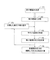
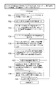
- FIG. 1 illustrates one aspect of an outline of processing performed by the information processing apparatus.
- the information processing apparatus first determines an atomic structure including atomic coordinates by simulation using empirical parameters (F1).
- FIG. 2 illustrates a simulation procedure when determining the atomic structure.
- an outline of a simulation for obtaining an atomic structure in a substance that is, atomic coordinates, will be described as a premise for calculating a stress distribution by the information processing apparatus.
- FIG. 2 is an example of a processing flowchart for obtaining an atomic structure in a substance.
- the CPU of the information processing apparatus executes a computer program that is developed on the memory so as to be executable, and executes the simulation illustrated in FIG.
- the processing when the CPU executes the computer program will be described simply as processing of the information processing apparatus.
- the information processing apparatus sets the initial value of the kind of atom and the position of the atom contained in the simulation target substance according to the user's specification (F11).
- the type of atom and the initial value of the atom position may be set in a parameter file on an external storage device such as a hard disk read by the information processing apparatus.
- the parameter may be set in a format such as (atom type, X, Y, Z).
- X, Y, and Z are values of three-dimensional coordinates that set the center of the atom.
- the crystal structure of an existing substance may be displayed on the display, and the user may change the crystal structure by manual operation.
- the manual operation refers to an operation of deforming the crystal structure displayed on the display with a pointing device such as a mouse.
- the crystal structure displayed on the display may be dragged with a mouse cursor.
- a menu that causes cutting, cracking, or the like may be provided in a part of the existing crystal structure so that the crystal structure can be edited on the display in accordance with the user's menu selection.
- a menu in which atoms of the same type as the atoms in the crystal or other types of atoms can be inserted in the crystal structure may be provided.
- the initial value of the position of the atom desired by the user is set by reading data from the parameter file or by modifying the existing crystal structure.
- the information processing apparatus uses the matrix elements obtained in F12, H ij ( ⁇ i , ⁇ j ), S ij ( ⁇ i , ⁇ j ), and solves the simultaneous equations of Equation 4 to obtain c i Ask. Then, the information processing apparatus, using c i obtained, obtains the wave function is a solution of Schrodinger equation in the same form as Equation 3.
- the information processing apparatus obtains the force acting between the atoms based on the wave function obtained in F3 (F14).
- the force acting between atoms for example, the binding force by the electrons of the outermost shell of atoms can be exemplified.
- the information processing apparatus obtains the sum of the forces acting on each atom according to the forces acting between the atoms.
- the information processing apparatus determines whether the sum of forces is less than a predetermined allowable value for each atom.
- the information processing apparatus confirms all the atoms to be simulated and determines whether or not the force acting on the atoms is less than a predetermined allowable value EPS (F15). Then, when the force acting on all the atoms to be simulated is less than the predetermined allowable value EPS, the information processing apparatus ends the simulation.
- the information processing apparatus moves each atom by a predetermined amount ⁇ in the direction of the force.
- the moving direction of the atoms is the direction of the force acting on each atom, while the predetermined amount ⁇ for moving the atoms may be a value common to the atoms to be simulated. Also, the predetermined amount ⁇ for moving the atom may be a value corresponding to the force acting on the atom. Then, the information processing apparatus returns the control to F2, and obtains the potential around the atom again.
- the information processing apparatus repeats the processes from F2 to F6 until the force acting on the atoms becomes less than the predetermined allowable value EPS. With this procedure, the information processing apparatus obtains a stable atomic structure with respect to the initial value of the atom position set in F1.
- a method for obtaining a stable position of an atom as shown in FIG. 2 is called atomic structure optimization, and the steepest descent method or the conjugate gradient method is generally used.
- the atomic structure obtained at this time is a structure with the lowest internal energy at absolute zero.
- the process for obtaining the atomic structure at a specific temperature and pressure is also executed by a computer system to which a technique called molecular dynamics calculation is applied.
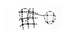
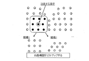
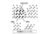
- FIG. 3 is a processing example in which a micro region is obtained from the atomic structure of a substance. In the example of FIG. 3, a combination of atoms included in a portion surrounded by a circle is extracted as a minute region.
- the information processing apparatus calculates the stress acting on the divided micro area.
- the information processing apparatus approximates a divided micro area to a parallelepiped and sets a virtual system in which the divided micro areas are periodically arranged.
- a common theory has been established for both the method using empirical parameters and the method not using it. Therefore, this information processing device sets the virtual system in which the divided micro-regions are arranged periodically, performs quantum calculation based on the established theory, and calculates the average value of stress in the virtual system. enable.
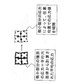
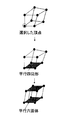
- FIG. 4 is an example of processing for creating a parallelepiped from a minute region.
- the information processing apparatus replaces the minute region extracted from the atomic structure by the processing of F2 with a parallelepiped having a parallelogram with a bottom surface and a predetermined translation vector.
- FIG. 4 shows a plan view of a parallelepiped viewed from one axial direction.
- the information processing device calculates the stress acting on the parallelepiped (F4).
- the information processing apparatus assumes a three-dimensional structure in which the parallelepiped obtained in F3 is repeated infinitely. Then, the information processing apparatus obtains an average value of stress acting on one parallel hexahedron in a regular parallel hexahedron repeating structure. Then, the information processing apparatus determines the average value of the obtained stress as the stress in the minute region. Then, the information processing apparatus repeats the processes of F3 and F4 as many times as the number of minute areas obtained in F2 (F5).
- the stress for each minute region in the substance is obtained.
- the stress for each micro region can be referred to as the stress at the boundary surface of the micro region (see FIG. 5).
- the information processing apparatus interpolates stresses other than the boundary surface of the micro area based on the stress for each micro area, and obtains a stress distribution (F6).
- FIG. 5 shows an example of processing for interpolating the stress at an arbitrary position from the stress on the boundary surface of the minute region.
- the information processing apparatus obtains the stress distribution of the substance obtained by the processing of F1. ⁇ Division of atomic structure into small regions>
- the details of the processing of F2 in FIG. 1 will be described.
- a method for dividing a material having a nanoscale structure that is, a material that has not completely formed a crystal structure into fine regions will be described below. If the division is simply performed in a grid pattern, there is a possibility that the atomic structure that affects the stress calculation is different between the real system and the virtual system in which minute regions are periodically arranged.
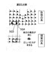
- Figure 6 shows an example of inappropriate division.
- the actual system illustrates the atomic structure of the actual material.
- the virtual system has an atomic structure determined by simulation as shown in FIG. As shown in FIG. 6, there may be a portion that does not necessarily match between the real system and the atomic structure of the virtual system determined by the simulation.
- micro regions SQ1 and SQ2 are both micro regions obtained by cutting the virtual atomic structure into a fixed mesh.
- the atomic structure of the virtual system obtained by the simulation is divided into minute regions, it is desirable to create the minute regions according to the atomic structure in the actual substance as much as possible. For example, even if the actual material contains crystal structure distortion, lattice defects, transitions, grain boundaries, impurity atoms, etc., and the atomic structure deviates from the positional relationship between atoms of the original material, It is desirable to create a minute region in accordance with the atomic structure of the substance. By creating a small region that matches the atomic structure in the actual material, even if the atomic structure of the virtual system does not match the actual system, the calculation result of the stress distribution in the virtual system is the stress of the actual system. This is because the possibility of similarity to the distribution increases.
- Fig. 7 shows an example of creating a micro area that is considered desirable.
- the example of FIG. 7 includes a portion of SQ3 that is close to the actual regular atomic structure and a portion of SQ4 that is adjacent to SQ3 and in which the distance between the atoms is compressed.
- this information processing apparatus instead of dividing into fixed areas as shown in FIG. 6, positions between atoms included in the basic lattice in the original atomic structure, such as SQ3 and SQ4 Prioritizing the relationship corresponding to the relationship, a minute region is created. Therefore, the crystal structure known for the atomic species of the substance is used as a reference model for the actual atomic structure of the substance.
- this information processing apparatus does not divide into fixed regions, but compares, for example, the relationship between the unit lattice or the basic lattice in the actual crystal lattice and the atomic structure of the virtual system, A unit cell in the lattice or a combination of atoms corresponding to the basic lattice is extracted and set as a minute region. Therefore, even if the atomic structure in the virtual system is distorted, the information processing apparatus is in a state in which the atomic structure corresponding to the unit cell in the actual crystal lattice or the basic lattice is distorted. Find the place where it is, and make it a minute area.
- the unit cell refers to a cell in which the side length is usually the shortest among the repeated structures of the crystal.
- a unit cell is called a unit cell.
- a repeating structure obtained by combining a plurality of unit lattices may be defined as a repeating unit.
- a crystal repetitive structure including a combination of a plurality of unit cells is also called a basic lattice or a basic cell.
- the term “unit cell” is used to mean both a unit cell and a basic cell.
- the information processing apparatus extracts an atomic structure corresponding to a unit cell or a basic lattice in an actual crystal lattice from the simulated atomic structure of a virtual system.
- the relationship between the micro region of interest and the atomic structure around the micro region is similar to the relationship between the unit lattice of the actual crystal lattice and the surrounding atomic structure. Therefore, even if microregions are individually extracted and replaced with parallelepipeds, and the average value of stress is obtained from a regular array of parallelepipeds, the relationship between the microregions and the atomic structure around the microregions is It can be close to this material.
- the information processing apparatus first identifies one or more crystal structures when the focused atom and neighboring atoms form a crystal from the atomic species of the focused atom and the atomic types of the atoms in the vicinity of the focused atom. . Then, the information processing apparatus determines the shape of the minute region on the basis of the basic lattice having the specified crystal structure, and divides the substance into the minute regions. The reason why the unit cell is used is that it is suitable for periodically arranging minute regions in the processing of F3 in FIG.
- FIG. 8 to FIG. 14 show specific procedures for dividing the virtual system into minute regions.
- FIG. 8 is a flowchart illustrating a processing procedure for dividing the virtual system into minute regions.
- FIG. 9 to FIG. 14 are examples of the process of dividing the atomic structure into minute regions by the information processing apparatus.
- the processing illustrated in FIGS. 8 to 14 is also processing performed by the CPU of the information processing apparatus executing a computer program that is executably expanded on the memory.
- FIG. 15 illustrates a format of a database of crystal structures included in the information processing apparatus.
- this information processing device prepares the lattice constant, unit vector, and atomic coordinate data corresponding to the crystal structure and atomic species in advance and stores them in the crystal structure database. Yes.
- a silicon atom is illustrated as an atomic species.
- a lattice constant a unit vector of the crystal structure, and atomic coordinates are defined.
- the lattice constant is the length of the lattice.
- lattice constant for lattices other than the cubic lattice, generally three lattice constants are defined.
- the first axial direction, the second axial direction, and the third axial direction refer to crystal lattice directions, respectively.
- a hexahedron when a hexahedron is assumed in the crystal of a substance, there may be a substance that cannot define a hexahedron so that atoms exist at all positions of eight vertices. However, for example, if a hexahedron having atoms at five vertices can be defined among the eight vertices of the hexahedron, the position of the vertex at which no atom exists can be specified from the atomic coordinates of the five vertices.
- the information processing apparatus estimates a vertex position where an atom does not exist from a vertex of a hexahedron where an atom exists for a substance where an atom does not exist at a part of the vertex of the hexahedron.
- the vertex of the hexahedron can be estimated based on the lattice constants a, b, and c.
- the vertex can be specified as a position obtained by adding or subtracting a / 2, b / 2, or c / 2 to the position (0, 0, 0) of the atom. Therefore, the vertex of the hexahedron of the crystal structure can be determined from the position of the atom by maintaining the functional relationship between the coordinates of the atom and the vertex coordinates of the hexahedron.
- the unit vector is a three-axis unit vector of the crystal lattice.
- the unit vector is a three-axis unit vector of the crystal lattice.
- FIG. 15 for example, three unit vectors (a1x, a1y, a1z), (a2x, a2y, a2z), and (a3x, a3y, a3z) are shown.
- atomic coordinates are coordinates indicating the position of atoms in the crystal.
- the origin of atomic coordinates is set at a predetermined position in the crystal, for example, the center of the crystal, one vertex of the crystal lattice, or the like.
- the reason why the atomic coordinates are included in the crystal structure database is that even if the crystal lattice can be created with the unit vector and the lattice constant, the atomic coordinates are not always at the vertex of the lattice.
- the information processing apparatus selects one atomic coordinate from atomic coordinate data obtained by simulation (F21).
- the information processing apparatus checks the selected atom and the atomic species of the selected nearby atom (F22).
- the neighborhood may be, for example, a selected atom and an atom placed at a position adjacent to the selected atom in the atomic structure.
- the information processing apparatus lists from the crystal structure database the crystal structures that can be taken when the selected atom and the atomic species of the selected nearby atoms form a crystal.
- the information processing apparatus takes out the lattice constant, unit vector, and atomic coordinates of each crystal structure from the crystal structure database (F23).
- the crystal structure of the silicon atom is a diamond structure or a ⁇ -tin structure.
- a diamond structure and a ⁇ -tin structure are respectively defined in the crystal structure database in the format of FIG. Therefore, this information processing apparatus extracts, for example, two lattice constants, unit vectors, and atomic coordinates for silicon atoms from a database of crystal structures.
- FIG. 9 illustrates crystal structures listed for the atom selected by F21 and the atomic species of the selected nearby atoms.
- the atom selected in F21 is the atom of interest.
- the information processing apparatus selects one crystal structure from several crystal structures listed (F24). Then, the information processing apparatus takes out atomic coordinates in a sphere centered on the atom selected in F21 and having a radius of twice the lattice constant from the atomic coordinate data of the substance obtained by simulation (F25).
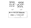
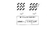
- the root mean square (RMS) of the difference between the atomic coordinates obtained from the simulation and the atomic coordinates in the atomic structure in the selected crystal structure database is calculated (F26).
- the minimum root mean square (RMS) of the difference in atomic coordinates of the atomic structure is selected.
- the root mean square (RMS) of the difference between the atomic coordinates obtained from the simulation and the atomic coordinates in the atomic structure in the selected crystal structure database corresponds to the evaluation value of the relative distance. For example, it is assumed that there is an atomic coordinate of T1-Tk in addition to the coordinate of the atom selected in F21 in a sphere having a radius that is twice the lattice constant.
- the information processing apparatus matches the position of the atom selected in F21 with the position of any atom in the crystal lattice. Then, the information processing apparatus extracts the positions of atoms (for example, from P1 to Pk) other than the position in the crystal where the atom selected in F21 is located. Then, the information processing apparatus calculates the root mean square (RMS) of the distance between atoms between the atomic coordinates T1 to Tk obtained from the simulation and the atomic positions P1 to Pk in the crystal. Calculate according to the following formula.
- RMS root mean square
- the crystal structure database holds atomic coordinates for each crystal structure of the atomic species. Therefore, if the crystal structure can be listed, the information processing apparatus can detect the crystal in the atomic species. The position of atoms in the structure can be specified.
- FIG. 10 shows a calculation example of the root mean square (RMS) of the distance between atoms.
- RMS root mean square
- the information processing apparatus repeats a series of procedures F22-F26, that is, selection of crystal structure, extraction of data from atomic coordinates obtained from simulation, and calculation of RMS for all crystal structures listed (F27). .
- this information processing apparatus compares the RMS calculated for each crystal structure, and determines the unit cell of the crystal structure having the smallest RMS. Then, this article processing apparatus determines the shape of the region to be divided with reference to the unit cell having the smallest RMS (F28). That is, the information processing apparatus obtains atomic coordinates obtained from simulation corresponding to atoms in a unit cell having a crystal structure with the smallest RMS. Then, a minute region formed by atomic coordinates obtained from simulation corresponding to an atom in a unit cell having a crystal structure with the smallest RMS is obtained.
- FIG. 11 illustrates a procedure for determining a minute area to be divided.
- the root mean square (RMS) of the difference in distance between atoms is minimized by associating the atomic positions P1-P4 in the crystal with the atomic coordinates T1-T4 in the substance obtained from the simulation.
- the information processing apparatus sets a region obtained by the atomic coordinates T1-T4 as a minute region.
- the position of the vertex where the atom exists is estimated from the vertex where the atom exists. For example, when there are no atoms at 3 vertices out of 8 vertices, a hexahedron with the smallest RMS may be created for 5 vertices with atoms. If there are atomic coordinates at positions other than the eight vertices of the unit cell in the crystal, first, the RMS of the coordinate difference value between the atom in the crystal structure and the atom in the simulated material is calculated. Find the smallest correspondence.
- the functional relationship between the coordinates specifying the position of the hexahedron obtained from the lattice constant is obtained with respect to the atomic coordinates in the crystal.
- the functional relationship of the coordinates may be applied to the simulated atomic coordinates of the substance corresponding to the atomic coordinates in the crystal to obtain a minute region of the substance.
- the minute region has a hexahedral shape.
- the predetermined limit value may be set in the memory as a parameter of the information processing apparatus such as N times the lattice constant using a predetermined integer N, for example.
- the information processing apparatus performs the operation of F22-F29 on the atomic coordinates obtained by the simulation (F2A), and divides the region.
- FIG. 12 to FIG. 14 show processing examples divided on the basis of other crystal lattices.
- FIG. 12-14 shows an example of processing when two atoms exist in the basic lattice of the crystal.
- FIG. 12 shows examples of atoms selected by F21, atomic species of selected nearby atoms, and crystal structures listed.
- the information processing apparatus searches the crystal structure database based on the atoms selected in F21 and the atomic species of the selected nearby atoms, and lists the crystal structures.
- the position of atoms in the crystal is associated with the atomic coordinates obtained from the simulation, and the case where the root mean square (RMS) of the difference in distance between atoms is minimized is obtained.
- the case where the root mean square (RMS) of the difference in distance between atoms is minimized is obtained.
- FIG. 14 based on the correspondence that minimizes the root mean square (RMS) of the difference in distance between the atoms in each crystal structure, it is obtained from the simulation corresponding to the atoms in the basic lattice of the crystal. Find the atomic coordinates.
- Br require lattice is used to characterize the translational symmetry of crystals.
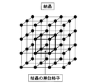
- FIG. 16A shows a crystal structure of a simple cubic lattice.
- FIG. 16A can be said to be an ideal crystal structure.
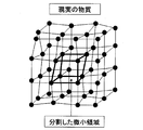
- FIG. 16B exemplifies an actual substance or a virtual atomic structure obtained by simulation with the same atomic species as FIG. 16A. As shown in FIG. 16B, the atomic structure of an actual substance or the atomic structure of a virtual system obtained by simulation often takes a distorted structure that deviates from the ideal crystal structure.
- the atomic structure of an actual substance or the virtual atomic structure obtained by simulation is divided into small regions whose dimensions and shapes are fixed, a micro region corresponding to the crystal structure peculiar to the atomic species is obtained. It is not possible.
- the difference in the distance between the atoms between the atoms in the crystal structure and the atoms in the real substance or in the virtual atomic structure obtained by simulation is determined.
- the root mean square (RMS) is minimum, the original crystal structure of the atomic species can be distorted.
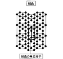
- FIG. 17A is an example of a crystal structure having a hexagonal close-packed structure.
- the coordinates of the atom are located at the vertex of the hexagonal column, the center of the end surface, and the end surface of the hexagonal column, and the atom located at the center of the end surface.
- the two rectangles are defined as end surfaces.
- a triangular prism with two triangles as end faces are also arranged at the center of the quadrangular prism.
- the triangular prism is combined with a triangular prism included in an adjacent hexagonal prism to form a quadrangular prism, and atoms are arranged at the center of the formed quadrangular prism.
- a hexahedron can be defined at the position indicated by the letters “crystal unit cell” by the arrows in FIG. 17A.
- FIG. 17B is an example of a virtual atomic structure obtained by simulation for estimating the atomic structure of an actual substance with the same atomic species as the crystal of FIG. 17A. If RMS has a minimum between a hexagonal close-packed structure crystal structure atom and a virtual atomic structure atom having a simple hexagonal Bravey lattice, the information processing apparatus As shown, the bottom surface is divided into a shape close to a rhomboid quadrangular prism. The size of the division may be about the volume of the unit cell in the crystal.
- ⁇ Deformation of micro area into parallelepiped> As described with reference to F3 and F4 in FIG. 1, in order to periodically arrange the divided minute regions, the regions need to be transformed into parallelepipeds. The reason is that in order to calculate the stress in a micro region, it is necessary to prepare a periodic structure created by the translation operation of the micro region, and the polyhedron that can fill the three-dimensional space by the translation operation is a parallelepiped. It is. In addition, the periodic structure is prepared for applying a calculation method based on a generally known quantum theory. This information processing apparatus performs deformation such that the root mean square (RMS) of the displacement from the original atomic arrangement is minimized in order to minimize the change in local stress due to deformation.
- RMS root mean square
- FIG. 18A is a flowchart illustrating a deformation process from a minute region to a parallelepiped.
- FIG. 18B illustrates a deformation process from a minute region to a parallelepiped using a figure.
- the processes of FIGS. 18A and 18B are also processes performed by the CPU of the information processing apparatus executing a computer program that is executably expanded on the memory.
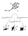
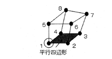
- the information processing apparatus selects one vertex from among the eight vertices of the micro area extracted by the processing of F2 in FIG. 1 (F31).
- the position of the selected vertex is illustrated in FIG. 18B.
- the information processing apparatus selects the remaining three vertices used for creating the parallelogram including the vertices selected in F31 (F32). Since a hexahedron is assumed as a micro-region deformed into a parallelepiped, the process of F32 is a process of selecting the other three vertices that form a quadrangle together with the vertices selected in F31.
- FIG. 19 illustrates the process of selecting three vertices.
- unit vectors (a1 ⁇ >, a2 ⁇ >, a3 ⁇ >) of the spatial grid used as a reference in determining the shape of the region in the processing of F2 in FIG. 1 are used.
- the vector a1 is displayed as "a1->”.
- the selected atom when the selected atom is the origin, there are the following three ways of selection. (1) three atoms corresponding to lattice points located at a1->, a2->, a1-> + a2->; (2) three atoms corresponding to lattice points located at a2->, a3->, a2-> + a3->; (3) Three atoms corresponding to lattice points located at a3->, a1->, a3-> + a1->; A parallelogram is created for the above three patterns.
- the information processing apparatus displaces the other three vertices so that the area surrounded by the selected vertex and the other three vertices becomes a parallelogram (F33).
- the parallelogram has an arbitrary side length, and there is no limitation on the angle of the plane formed by the parallelogram. The process of F33 will be described in more detail with reference to FIGS.
- the information processing apparatus creates a parallelepiped.
- This information processing apparatus processes according to the definition that “two planes are congruent and parallel with two parallel planes, and the remaining four planes are parallelograms”. Execute. That is, the information processing apparatus creates a parallelepiped candidate obtained by translating the parallelogram created in F33. Here, the remaining four vertices in the minute area other than the four vertices selected in the processing of F32 and moved to become a parallelogram in F33 are moved.
- the information processing apparatus creates parallel hexahedrons by displacing the remaining four vertices so that the apexes of the parallel hexahedron candidates overlap the vertices of the minute region (F34).
- F34 The process of F34 will be described in more detail with reference to FIG.
- the information processing apparatus changes three vertices other than the selected vertex, and repeats the process of F33 (F35). Further, the information processing apparatus changes the selected vertex and executes the operation of F32 to F35 performed on the eight vertices in the area (F36).
- the information processing apparatus calculates the RMS of the seven vertices moved, that is, the displacement of the atom, and uses the parallelepiped having the smallest RMS as a virtual unit cell (F37). In the above procedure, a large number of parallelepipeds are created, but the only parallelepiped can be obtained under the condition of “selecting a parallelepiped that minimizes the RMS of displacement of the moved atom”.
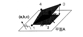
- FIG. 20 illustrates the process of F33 in FIG. 18A, that is, the parallelogram creation process.
- the atoms are labeled as shown in FIG.
- Formulas 5 and 6 are established on the condition that the lengths of opposite sides are equal.
- FIG. 23 illustrates two types of parallelograms obtained by solving Equations 5 and 6.
- the above operation changes the normal vector value and the four variables x2, x3, y2, and y3 to prepare various parallelograms.
- the procedure for changing x2, x3, y2, and y3 is illustrated below.
- the range of change of x2, x3, y2, and y3 is within a sphere having a radius set by the user from the original atomic position.
- the increment of change is the mesh width obtained by equally dividing the sphere.
- the range of change is polar coordinate display, where ⁇ is 0 ° ⁇ ⁇ 180 ° and ⁇ is 0 ° ⁇ ⁇ 360 °.
- the step size is a step size set by the user with respect to ⁇ and ⁇ in the polar coordinate display.
- a parallelogram is prepared when x2, x3, y2, y3, a, b, and c are changed in the above-mentioned range in the above range.
- FIG. 22 shows an example of a changed parallelogram.
- FIG. 20 is a flowchart illustrating parallelogram creation processing by the information processing apparatus.
- the information processing apparatus gives an initial value of the normal vector (a, b, c) of the plane A including the atom 1 (F321).
- ⁇ and ⁇ are increments when ⁇ and ⁇ are changed, respectively.
- it may be a normal vector of a plane including the center coordinates of atoms 1, 2 and 3.
- the information processing apparatus gives initial values of four variables (x2, x3, y2, y3) (F322).
- the initial values of the four variables (x2, x3, y2, y3) may be, for example, end points of meshes that are cut at equal intervals in a sphere having a radius set by the user.
- the information processing apparatus solves Expression 2 to Expression 6 to obtain (x4, x4, z2, z3, z4), and creates a parallelogram on the plane A.
- the information processing apparatus changes the four variables (x2, x3, y2, y3) by a predetermined step size (F324). Then, the information processing apparatus returns the control to F323. In this way, the information processing apparatus executes the process of F323 within the sphere having the radius set by the user from the original atomic position.
- the information processing apparatus changes the normal vector (a, b, c) of the plane (F325). Then, the information processing apparatus returns control to F322. In this way, the information processing apparatus displays polar coordinates, changes the normal vector in the range of ⁇ 0 ° ⁇ ⁇ 180 °, ⁇ 0 ° ⁇ ⁇ 360 °, and repeats the processing of F322 and F323. Execute.
- FIG. 24 is a flowchart illustrating the process of F34 in FIG. 18A, that is, the parallelepiped creation process.
- FIG. 25 illustrates a parallelogram before parallelepiped formation, that is, before movement.
- FIG. 26 illustrates a parallelogram before parallel hexahedron formation, that is, before and after movement.
- the information processing apparatus determines a translation vector (p, q, r) for translating the created parallelogram (F340).
- a translation vector p, q, r
- the information processing apparatus newly prepares a coordinate system so that the direction of the normal vector of the plane A including the parallelogram is the z-axis direction (F341).
- the information processing apparatus uses the x coordinate x1, x2, x3, x4 of the parallelogram before the movement and the parallelogram after the movement as the x component p of the translation vector of the movement.
- a change amount ⁇ 1 on the minimum value side and a change amount ⁇ 2 on the maximum value side are calculated between the x coordinates x5, x6, x7, and x8 of the shape.
- the calculation of the y component q of the translation vector is the same as that of the x component.
- the increment of change may be a user-specified value.
- the information processing apparatus translates the parallelogram according to the translation vector (p, q, r) to obtain a parallelepiped (F343). Then, the information processing apparatus displaces the atoms 5, 6, 7, and 8 so as to overlap the vertices of the parallelogram that has been translated. The above operation is performed for each translation vector, and a translation vector (p, q, r) that minimizes the RMS of the displacement is employed (F344). Then, the information processing apparatus creates a parallelepiped according to the adopted translation vector (p, q, r).
- the information processing apparatus is a method based on quantum theory using empirical parameters for virtual crystals in which parallel hexahedrons obtained by the processing of F3 in FIG. 1 are periodically arranged and periodically arranged. Then, the average value of stress is obtained. The average stress is determined according to Equation 9. Details of the stress average value calculation processing according to Equation 9 are as follows.
- the stress can be obtained as shown in Equation 10 by differentiating the total energy by the amount of strain ⁇ .
- Equation 1 When the tight binding method is used, the total energy can be expressed by Equation 1, and the stress is as follows.
- S ij of the number 5 shows the case of the unit matrix.
- R can be expressed as follows in the presence of distortion.
- this information processing apparatus assumes a structure in which a minute region of a substance is replaced with a parallelepiped and the parallelepiped is repeated infinitely in the X, Y, and Z directions.
- a parallelepiped is repeated infinitely in the X, Y, and Z directions.
- ⁇ > which means an average, can be simply transformed into an integral symbol within one parallelepiped.
- Equation 10 is an equation that averages the stress in the parallelepiped with the wave function ⁇ .
- the first term in the stress averaged by the wave function ⁇ in Equation 10, that is, the first term indicated by the product of the momentum operator, is an expression obtained by differentiating the kinetic energy of the atom once.
- This first term is a pressure term generated from the kinetic energy of the atom.
- the second term in the stress averaged by the wave function ⁇ is a term of pressure generated by potential, for example, Coulomb force.
- Equation 9 the average value of the stress of the parallelepiped can be obtained by Equation 9.
- Equation 9 or Equation 10 can be reduced to integration in the parallelepiped.
- the average stress in the parallelepiped obtained by the equation (9) is defined as the stress in the micro area of the substance.
- the local stress is obtained by linearly interpolating the stress obtained in each region.
- the stress value calculated in each minute region is the value of the barycentric coordinates of the eight atoms forming the parallelepiped.
- a stress function stress distribution in the entire space is obtained by performing linear interpolation.
- the center of gravity is (X1, Y1, Z1) in the minute region V1, and the stress Tyz1 in the X-axis direction is obtained. Further, it is assumed that the center of gravity of the minute region V2 adjacent to the minute region V1 is (X1 + D, Y1, Z1), and the stress Tyz2 in the X-axis direction is obtained.
- d is a distance from the center of gravity of the minute region V1.
- this information processing apparatus enables calculation of local stress and calculation of the distribution of calculated stress in a calculation method based on quantum theory using empirical parameters. Therefore, the range of physical quantities that can be obtained can be expanded.
- the information processing apparatus divides the atomic structure of the substance into micro regions based on the crystal structure of the atoms contained in the substance. Then, the information processing apparatus replaces the microregion obtained by the division with a parallelepiped, and creates a virtual crystal structure by repeating the parallelepiped. Since the virtual crystal structure may be considered as a uniform substance, the information processing apparatus obtains an average value of stress by integral calculation within one parallelepiped in the virtual crystal structure. The information processing apparatus uses the average value of the stress obtained in the virtual crystal structure as the stress in the minute region of the substance. By repeating the processing as described above, the information processing apparatus calculates the stress of each minute portion of the atomic structure of the substance. Therefore, the information processing apparatus can determine the stress distribution in the substance, that is, the local stress.
- the information processing apparatus divides the substance into minute parts based on the crystal structure of atoms contained in the substance, so the relationship between the minute part and the atomic structure around the minute part is A virtual crystal structure can be created in a state as similar to the original atomic structure as possible. Therefore, it can be considered that the average stress obtained from the virtual crystal structure is close to the stress acting on the minute portion in the substance.
- This information processing apparatus enables calculation of the average stress by the virtual crystal structure in a state where the physical properties inherent to the substance as described above are maintained as much as possible.
- this information processing device uses quantum theory using empirical parameters with relatively little computational load, it is important to understand the occurrence of defects and cracks in materials at the atomic level in the development of nanodevices.
- the local stress can be calculated in a practical time for a practical scale system composed of several thousand atoms or more.
- the information processing apparatus can calculate stress even for an atomic structure formed by processes other than the process of FIG. (3) Local stress calculation of only a necessary region is possible, and calculation cost can be reduced according to requirements.
- FIG. 28 illustrates the hardware configuration of the information processing apparatus according to the second embodiment.
- the information processing apparatus is a computer that can be connected to the network 30.
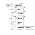
- the information processing apparatus includes a CPU 11, a memory 12, an external storage device such as a hard disk drive 13, a display 14, an operation unit 15, a communication unit 16, and a portable storage medium input / output device 17.
- the CPU 11 executes a computer program that is executable on the memory 12 and provides the functions of the information processing apparatus.
- the CPU 11 is not limited to one and may include a plurality of cores.
- the memory 12 stores a computer program executed by the CPU 11, data processed by the CPU 11, and the like.
- the memory 11 includes a non-volatile ROM (Read Only Memory) and a volatile DRAM (Dynamic Random Access Memory).
- the hard disk driven by the hard disk drive 13 stores a computer program developed in the memory 12 or data processed by the CPU 11.
- an SSD Solid State Drive
- the hard disk drive 13 or an external storage device such as an SSD is connected to the CPU 21 through the interface 13A.
- the interface 13A is an interface such as USB (Universal Serial Bus), IDE (Integrated Drive Electronics), SCSI (Small Computer System Interface), FC (Fibre Channel), and the like.
- USB Universal Serial Bus
- IDE Integrated Drive Electronics
- SCSI Small Computer System Interface
- FC Fibre Channel
- the display 14 is, for example, a liquid crystal display, an electroluminescence panel, or the like.
- the display 14 is connected to the CPU 21 through the interface 14A.
- the interface 14A is, for example, a graphics module such as VGA (Video Graphics Array) or an interface such as DVI (Digital Visual Interface).
- the operation unit 15 is an input device such as a keyboard, a mouse, a touch panel, and an electrostatic pad.
- the electrostatic pad is a device used to detect a user operation of tracing a flat pad with a finger or the like, and to control the position and movement state of the cursor on the display in accordance with the user operation. For example, the movement of the user's finger is detected by a change in the capacitance of the electrode under the flat pad.
- the operation unit 15 is connected to the CPU 11 through the interface 15A.
- the interface 15A is, for example, a USB interface.
- the communication unit 16 is also called NIC (Network Interface Card).
- the communication unit 16 is, for example, a LAN (Local Area Network) interface.
- the communication unit 16 is connected to the CPU 11 through the interface 16A.
- the interface 16A is an expansion slot connected to the internal bus of the CPU 11, for example.
- the portable storage device 17 is an input / output device such as a CD (Compact Disc), a DVD (Digital Versatile Disk), a Blu-ray disc, or a flash memory card.
- the portable storage device 17 is connected to the CPU 11 through the interface 17A.
- the interface 17A is an interface such as USB or SCSI, for example.
- the information processing apparatus may be a plurality of computers in which a plurality of computers cooperate with each other and execute processing in a shared manner.
- FIG. 29 illustrates a functional configuration of the information processing apparatus according to the second embodiment.
- This information processing apparatus has a crystal structure database 24 and a substance atomic structure file 25 on an external storage device such as a hard disk.
- the crystal structure database 24 corresponds to a means for storing an atomic structure including atomic positions in the crystal.
- the substance atomic structure file 25 corresponds to means for storing an atomic structure including an atomic position in the substance.
- At least one of the crystal structure database 24 and the substance atomic structure file 25 may be in a device other than the external storage device of the information processing device, for example, the memory 12. Further, at least one of the crystal structure database 24 and the substance atomic structure file 25 may be in a storage device on a network, for example, SAN (Storage Area Network). Further, at least one of the crystal structure database 24 and the substance atomic structure file 25 may be on another computer on the network, for example, a database server, accessible through the network.
- SAN Storage Area Network
- the format of the crystal structure database 24 is the same as that shown in FIG.
- the atomic structure file 25 of the substance is obtained by the atomic structure optimization process using the empirical parameters described in the first embodiment, for example, the steepest descent method or the conjugate gradient method.
- the atomic structure file 25 of the substance includes a large number of records including, for example, the atomic species (ATYPEi), the X coordinate (Xi), the Y coordinate (Yi), and the Z coordinate (Zi) of the atom.
- the CPU 11 executes a program that is executed in the memory 12 so as to be executable, and functions as the control means 21, the dividing means 22, and the divided partial average stress calculating means 23 of the substance.
- the dividing means 22 reads the position of the atom contained in the atomic structure of the substance from the atomic structure file 25 of the substance. Then, the dividing means 22 compares the atomic position in the divided portion obtained by dividing the substance into a plurality of atoms and the atomic position in the crystal containing the atoms. Then, the dividing unit 22 compares the atomic position of the divided part obtained by dividing the substance into a plurality of atoms and the atomic position of the crystal including the atoms of the substance, and the relative distance between corresponding atoms between the divided part and the crystal. The atomic position of the divided portion is associated with the atomic position of the crystal so that the evaluation value of is the smallest.
- the dividing unit 22 specifies a divided part of the substance corresponding to the unit cell of the crystal.
- the divided portion corresponds to, for example, a minute portion of the substance referred to in Example 1.
- the parallelepiped forming means 23 acquires the divided part of the substance divided by the dividing means 22.
- the divided portion is, for example, a hexahedron.
- the parallelepiped forming unit 23 determines a parallelepiped that minimizes the evaluation value of the relative distance between the vertex of the divided portion and the vertex of the parallelepiped.
- the processing procedure of the parallelepiped forming means 23 in this case is the same as the processing of FIGS. 18A to 24 shown in the first embodiment.
- the average stress calculation means 24 creates a virtual crystal structure in which the parallelepipeds created by the parallelepiped formation means 23 are repeated. Then, the average stress calculation unit 24 calculates the average stress of the virtual crystal structure according to the same calculation formula as the formula 10 shown in the first embodiment.
- the control means 21 processes the atomic structure file 25 of the substance using the dividing means 22, the parallelepiped forming means 23, and the average stress calculating means 24. That is, the atomic structure given by the atomic structure file 25 of the substance is divided into divided parts, the divided parts are changed to parallelepipeds, a virtual crystal structure is generated, and the average stress obtained from the virtual crystal structure is calculated for the divided parts. Let it be stress.
- the control unit 21 repeatedly executes the dividing unit 22, the parallelepiped forming unit 23, and the average stress calculating unit 24 to create a stress distribution generated in the atomic structure given by the atomic structure file 25 of the substance.
- the stress distribution can be expressed as (Xi, Yi, Zi, Txyi, Tyzi, Tzxi) by using the center of gravity (Xi, Yi, Zi) of the divided portion and can be stored in the memory 12, for example.
- the average stress obtained by the uniform stress calculation means 24 is a stress acting on the divided portion divided by the dividing means 22, that is, acts on the boundary surface between the divided portion and another divided portion.
- the stress at a position other than the boundary surface between the divided portion and the other divided portions is obtained by the control means 21 by linear interpolation according to the distance from the boundary surface.
- the control means 21 outputs the stress distribution in the substance given by the atomic structure file 25 of the substance.
- the output destination of the stress distribution is, for example, a file in the external storage device, the display 14A, a variable area of another application program in the memory 12, or the like.
- Computer-readable recording medium A program for causing a computer or other machine or device (hereinafter, a computer or the like) to realize any of the above functions can be recorded on a recording medium that can be read by the computer or the like.
- the function can be provided by causing a computer or the like to read and execute the program of the recording medium.
- a computer-readable recording medium is a recording medium that stores information such as data and programs by electrical, magnetic, optical, mechanical, or chemical action and can be read from a computer or the like.
- Examples of such a recording medium that can be removed from a computer or the like include, for example, a memory such as a flexible disk, a magneto-optical disk, a CD-ROM, a CD-R / W, a DVD, a Blu-ray disc, a DAT, an 8 mm tape, and a flash memory.
- a recording medium fixed to a computer or the like there are a hard disk, a ROM (read only memory), and the like.
Landscapes
- Engineering & Computer Science (AREA)
- Computing Systems (AREA)
- Theoretical Computer Science (AREA)
- Physics & Mathematics (AREA)
- Health & Medical Sciences (AREA)
- General Health & Medical Sciences (AREA)
- Spectroscopy & Molecular Physics (AREA)
- Life Sciences & Earth Sciences (AREA)
- Bioinformatics & Cheminformatics (AREA)
- Bioinformatics & Computational Biology (AREA)
- Management, Administration, Business Operations System, And Electronic Commerce (AREA)
Abstract
情報処理装置は、物質中の原子位置を含む原子構造を記憶する手段と、原子を含む結晶中の原子位置を含む原子構造を記憶する手段と、物質を複数に分割した分割部分の原子位置と原子を含む結晶の原子位置とを比較し、分割部分と結晶との間で対応する原子間の相対距離の評価値が最も小さくなるように、分割部分の原子位置と結晶の原子位置とを対応付け、結晶の単位格子に相当する、物質の分割部分を特定する分割手段と、分割部分の頂点と平行六面体の頂点との間で相対距離の評価値が最も小さくなるような平行六面体を決定する平行六面体形成手段と、平行六面体を繰り返した仮想結晶構造において平行六面体に加わる平均応力を算出する平均応力算出手段と、部分特定手段、平行六面体形成手段、平均応力算出手段を繰り返し機能させることによって物質のそれぞれの分割部分の応力を特定する制御手段と、を備える。
Description
本発明は、物質の応力を算出する情報処理装置に関するものである。
ナノデバイスの開発を行う際に、量子論に基づくシミュレーションを用いる傾向が年々高まっている。なぜなら、ナノデバイスの微細化が進む現在において、目的にあったデバイス開発には、古典力学ではなく量子力学(量子論)が適用されるナノスケールでの物理現象を理解することが有効と考えられるからである。ナノスケールでの物理現象の一例として、物質中の欠陥・亀裂の発生が挙げられる。ナノスケールの欠陥や亀裂の発生の理解には、量子論が適用される微細な領域の原子構造の安定性をより詳細に調べることが有効である。いずれにしても、ナノスケールの欠陥や亀裂の発生の理解、あるいは、微細な領域の原子構造の安定性調査のためには、局所応力の計算が有用である。
量子論に基づいて物質のシミュレーションを行う際の計算手法には、タイトバインディング法など経験的パラメータを用いる計算手法と、経験的パラメータを用いない計算手法、例えば第一原理計算が存在する。
経験的パラメータを用いた量子論に基づく計算手法の1つであるタイトバインディング(Tight-Binding)法とは以下のような計算手法である。
通常、タイトバインディング法では、全系のエネルギーを以下のように表す。

右辺の第一項は電子と電子、電子とイオンの相互作用によるエネルギーを示す。また、第二項はイオンとイオンの相互作用によるエネルギーと第一項の補正を表す。また、εnは一電子ハミルトニアンの固有値である。すなわち、一電子のシュレーディンガー方程式

の固有値である。タイトバインディング法では、例えば、一電子のシュレーディンガー方程式の固有関数である波動関数を数3のように、原子軌道の和で表す。一電子のシュレーディンガー方程式とは、シュレーディンガー方程式を平均場近似と呼ばれる手法で近似した式である。したがって、一電子のシュレーディンガー方程式は、電子1個の系を取り扱う式という意味ではない。

ここで、φiは原子内の電子軌道、nは固有値のモード、R(太字)は並進ベクトル、τ(太字)iは原子の位置、k(太字)は波動関数の波数である。また、数式上太字で示されている、R(太字)、τ(太字)i、k(太字)を、明細書文中では、単に、R、τi、kのように通常のフォントで表すことにする。
このように波動関数を原子軌道で展開することによって、一電子のシュレーディンガー方程式(微分方程式)を解く問題を、原子軌道の係数を求める問題(固有値問題)に置き換える。具体的には、シュレーディンガー方程式の両辺に左から、Σl0exp(-ikRl0)φj
*(r-τj-Rl0)を掛け、全空間で積分することによって、一電子のシュレーディンガー方程式が固有値問題に置き換えられる。すなわち、

ここで、Hij(τi,τj),Sij(τi,τj)を以下のように定義した。

タイトバインディング法では、距離の関数であるHij(τi,τj),Sij(τi,τj)を、固有値などが実験値を再現するように人為的に決定する。このとき、経験的パラメータを用いる。また、タイトバインディング法の特徴として、求める係数ciの個数が(全系の原子数)×(1原子当たりの価電子数)で済むため計算負荷が軽いという特徴を持つ。例えば、100原子のシリコン原子の最外殻の電子を考慮してシミュレーションを行うためには、s軌道とp軌道の電子のみ扱う場合には400次元の固有値問題を解けばよいことになる。
一方、経験的パラメータを用いない量子論に基づく計算手法の1つとして、密度汎関数理論に基づく第一原理計算がある。その手法は以下の通りである。
第一原理計算では、原子単位系での全系のエネルギーは

と表すことができる。第一項目は電子の運動エネルギー、第二項目は電子間のクーロンエネルギー、第三項目は電子の交換相関項、第四項目は電子とイオンの相互作用エネルギー、第五項目はイオン間の相互作用エネルギーである。また、vext(r)はイオンが作るポテンシャルである。ここで、上記の|i(r)とn(r)は電子間の相互作用がない仮想系における一電子の波動関数と電子密度である。|i(r)とn(r)は、下記数7の方程式(Kohn Sham方程式)を自己無撞着に解くことによって計算することができる。

Kohn Sham 方程式を解く際には、波動関数を平面波で展開する方法が広く使われている。波動関数を平面波で展開した形式を数8に例示する。

このように波動関数を平面波で展開することによって、Kohn Sham方程式(微分方程式)を解く問題を、平面波の係数を求める問題(固有値問題)に置き換える。固有値問題を解く際は、タイトバインディング法と異なり経験的パラメータを用いずに行列要素を求める。また、第一原理計算の特徴として、平面波の係数の個数が非常に多いという特徴を持つ。これは、イオンがいるサイトに局在した波動関数を広がった平面波の重ね合わせで表現しなければならないためである。例えば、2原子を有するシリコン原子のシミュレーションに、数百次元の固有値問題を解く必要がある。したがって、経験的パラメータを用いない場合には、取り扱うことができる原子数がタイトバインディング法などの経験的パラメータを用いた場合と比較して少なくなる。
現在、周期的構造を持った結晶中の応力の平均値を求める方法として、両手法に共通して適用できる理論が存在する(非特許文献1)。具体的な方法は、以下の通りである。
(1)シュレーディンガー方程式を解き、結晶のエネルギーと原子に働く力を求め、原子構造最適化、もしくは分子動力学計算を行う。
(2)(1)で求めた原子座標とシュレーディンガー方程式の解である波動関数を用いて、応力の平均値を求める。応力の平均値は、以下の数9の式で表される。
(1)シュレーディンガー方程式を解き、結晶のエネルギーと原子に働く力を求め、原子構造最適化、もしくは分子動力学計算を行う。
(2)(1)で求めた原子座標とシュレーディンガー方程式の解である波動関数を用いて、応力の平均値を求める。応力の平均値は、以下の数9の式で表される。

ここで、Tαβは応力、rは原子座標、Ψは波動関数、miは原子iの質量、pにハット(^)を付した要素は運動量の演算子、Vはポテンシャルである。iは、原子を識別するラベル、Σは、系に含まれる原子についての加算である。なお、αβは、x,y,zのいずれか2つを意味する。したがって、Tαβは、Txx,Txy(=Tyx),Txz(=Tzx),Tyy,Tyz(=Tzy)のいずれかである。例えば、Txyは、x軸に垂直な面(YZ平面)に働くy方向の応力を意味する。
また、経験的パラメータを用いない計算手法においては、局所応力の計算手法も開発されている(非特許文献2)。開発されている手法の一例として密度汎関数理論に基づく第一原理計算を用いた局所応力の計算手法を挙げる。まず、基礎方程式であるKohn Sham方程式を解いて一電子波動関数と電子密度を求める。一電子波動関数と電子密度は三次元座標の関数として求めることができるので、密度汎関数理論では、全系のエネルギーが一電子波動関数および電子密度の汎関数で与えられる。したがって、エネルギーの微分量である応力も三次元座標の関数として得ることができ、局所応力を計算することができる。
O. H. Nielsen and R. M. Martin, Phys. Rev. ,米国,B 32, 3780 (1985)
A. Filippetti and V. Fiorentini, Phys. Rev. ,米国,B 61, 8433 (2000)
すでに説明したように、量子論に基づいた物質のシミュレーションには、経験的パラメータを用いた手法と経験的パラメータを用いない手法がある。現在、応力の平均値の計算については、両者の手法を用いて実行することが可能である。一方、応力分布すなわち局所応力の計算については、経験的パラメータを用いない手法に対して手法開発が行われている。しかし、経験的パラメータを用いない手法は、取り扱うことができる原子数が数十原子~数百原子程度であるという欠点を持つ。したがって、精度は落ちるものの高速計算が可能である経験的パラメータを用いた量子論に基づく手法で、局所応力を計算する方法の開発が課題となる。
ところで、経験的パラメータを用いない計算手法の場合には、数6に示したように、エネルギーが三次元座標の関数として与えられるので、エネルギーを三次元座標で微分することによって応力も三次元座標の関数として得ることができる。しかし、経験的パラメータを用いた計算手法の場合は、数1に示したように、エネルギーを三次元座標の関数をして表示することができないので、経験的パラメータを用いない手法のように微分操作により局所応力を得ることはできないという課題がある。
タイトバインディング法に代表される経験的パラメータを用いた量子論に基づく手法で局所応力を算出することができれば、現実的な数の原子を含むナノ構造、例えば、数千個以上の原子を含む物質における局所応力の計算が可能になると期待される。
そこで、開示の技術の目的は、経験的パラメータを用いた計算手法で得られた、三次元座標に対するエネルギー分布が得られない物質内の原子配置のシミュレーション結果に対して、物質内の応力分布を算出する技術を提供することにある。
開示の技術の一側面は、情報処理装置として例示できる。本情報処理装置は、物質中の原子位置を含む原子構造を記憶する手段と、原子を含む結晶中の原子位置を含む原子構造を記憶する手段と、物質を複数に分割した分割部分の原子位置と原子を含む結晶の原子位置とを比較し、分割部分と結晶との間で対応する原子間の相対距離の評価値が最も小さくなるように、分割部分の原子位置と結晶の原子位置とを対応付け、結晶の単位格子に相当する、物質の分割部分を特定する分割手段と、分割部分の頂点と平行六面体の頂点との間で相対距離の評価値が最も小さくなるような平行六面体を決定する平行六面体形成手段と、平行六面体を繰り返し配置した仮想結晶構造において平行六面体に加わる平均応力を算出する平均応力算出手段と、分割手段、平行六面体形成手段、平均応力算出手段を繰り返し機能させることによって物質のそれぞれ分割部分の応力を特定する制御手段と、を備える。
開示の技術によれば、経験的パラメータを用いた計算手法で得られた、三次元座標に対するエネルギー分布が得られない物質内の原子配置のシミュレーション結果に対して、物質内の応力分布を算出することができる。
以下、図面を参照してを実施形態に係る情報処理装置について説明する。以下の実施形態の構成は例示であり、本情報処理装置は実施形態の構成には限定されない。
本情報処理装置は、材料設計支援アプリケーションにおける、局所応力の計算手法に関する。特に、本情報処理装置は、ターゲット物質を微小領域に分割し周期構造を持った仮想系を想定することにより高速演算が可能な経験的パラメータを用いた量子論に基づいて局所応力を計算する。
経験的パラメータを用いた手法では、全系のエネルギーを三次元座標で表される一電子波動関数の汎関数で得ることができないので、経験的パラメータを用いない量子論による手法と同じ手段では、エネルギーの微分量である応力を三次元座標の関数として得ることができない。
そこで、本実施形態の情報処理装置は、物質の原子座標を求めるシミュレーション、例えば、原子構造最適化、もしくは分子動力学計算を行った後、計算した原子座標を用いて物質を微小領域に分割し、分割された物質の微小領域を平行六面体で近似する。そして、本情報処理装置は、その平行六面体を単位格子とする周期的構造を持った仮想系を想定することによって、微小領域の応力の平均値を計算する。最後に、本情報処理装置は、各微小領域の応力を補間することによって、応力分布を求める。
<処理手順>
図1に、本情報処理装置による処理概要の一側面を例示する。本情報処理装置は、まず、経験的パラメータを用いたシミュレーションによって、原子の座標を含む原子構造を決定する(F1)。図2に、原子構造を決定する場合のシミュレーションの手順を例示する。ここでは、本情報処理装置による応力分布算出の前提として、物質内の原子構造、すなわち、原子座標を求めるシミュレーションの概要を説明する。図2は、物質内の原子構造を求める処理フローチャートの例である。情報処理装置のCPUは、メモリ上に実行可能に展開されたコンピュータプログラムを実行し、図2に例示したシミュレーションを実行する。以下、CPUがコンピュータプログラムを実行するときの処理を単に情報処理装置の処理として説明する。
図1に、本情報処理装置による処理概要の一側面を例示する。本情報処理装置は、まず、経験的パラメータを用いたシミュレーションによって、原子の座標を含む原子構造を決定する(F1)。図2に、原子構造を決定する場合のシミュレーションの手順を例示する。ここでは、本情報処理装置による応力分布算出の前提として、物質内の原子構造、すなわち、原子座標を求めるシミュレーションの概要を説明する。図2は、物質内の原子構造を求める処理フローチャートの例である。情報処理装置のCPUは、メモリ上に実行可能に展開されたコンピュータプログラムを実行し、図2に例示したシミュレーションを実行する。以下、CPUがコンピュータプログラムを実行するときの処理を単に情報処理装置の処理として説明する。
図2の処理では、まず、情報処理装置は、ユーザの指定にしたがって、シミュレーション対象の物質に含まれる原子の種類と、原子の位置の初期値を設定する(F11)。原子の種類と、原子の位置の初期値は、情報処理装置が読み出すハードディスク等の外部記憶装置上のパラメータファイルに設定しておいてもよい。パラメータは、例えば、(原子の種類、X,Y,Z)のような形式で設定するようにしてもよい。ここで、X,Y,Zは、原子の中心を設定する3次元座標の値である。
また、例えば、ディスプレイ上に、既存の物質の結晶構造を表示し、ユーザがその結晶構造をマニュアル操作で変形するようにしてもよい。ここで、マニュアル操作とは、ディスプレイに表示された結晶構造を、マウス等のポインティングデバイスで変形する操作をいう。例えば、マウスカーソルでディスプレイに表示された結晶構造をドラッグできるようにしてもよい。また、既存の結晶構造の一部に、切断、亀裂等を生じさせるメニューを設けて、ユーザのメニュー選択に応じて、結晶構造をディスプレイ上で編集できるようにしてもよい。また、結晶構造中に、その結晶中の原子と同種類の原子、または他の種類の原子を挿入できるメニューを設けてもよい。ユーザが、結晶中に、原子を挿入する位置と、挿入される原子の種類を選択できるようにすればよい。以上のようなF1の処理にしたがい、パラメータファイルからのデータの読み出し、あるいは、既存の結晶構造の変形によって、ユーザが所望する原子の位置の初期値が設定される。
次に、現在の原子の位置と当該原子の原子種を基に、数5の行列要素を経験的パラメータを用いて設定する(F 12)。例えば、τiにシリコン原子、τjに水素原子が配置している場合には、r=|τi-τj|だけ離れたシリコン原子と水素原子の電子的性質を再現するように経験的パラメータを用いて行列要素を求める。
次に、情報処理装置は、F12で求めた行列要素、Hij(τi,τj),Sij(τi,τj)を用い、数4の連立方程式を解くことで、ciを求める。そして、情報処理装置は、求めたciを用いて、数3と同様の形式でシュレーディンガー方程式の解である波動関数を求める。
次に、情報処理装置は、F3で得られた波動関数を基に、原子間に作用する力を求める(F14)。原子間に作用する力としては、例えば、原子の最外殻の電子による結合力を例示できる。
次に、情報処理装置は、原子間に作用する力にしたがって、各原子に作用する力の和を求める。そして、情報処理装置は、それぞれの原子について、力の和が所定の許容値未満か否かを判定する。情報処理装置は、シミュレーションの対象の原子のすべてを確認し、原子に作用する力が、所定の許容値EPS未満であるか、否かを判定する(F15)。そして、シミュレーションの対象のすべての原子に対して、作用する力が所定の許容値EPS未満である場合、情報処理装置は、シミュレーションを終了する。
一方、シミュレーションの対象のいずれかの原子に作用する力が、所定の許容値EPS以上である場合、情報処理装置は、それぞれの原子を力の方向に所定量Δ移動する。なお、原子の移動方向はそれぞれの原子に作用する力の方向とし、一方、原子を移動する所定量Δは、シミュレーション対象の原子に共通の値でもよい。また、原子を移動する所定量Δについても、原子に作用する力に応じた値としてもよい。そして、情報処理装置は、制御をF2に戻し、再度、原子の周囲のポテンシャルを求める。
そして、原子に作用する力が所定の許容値EPS未満となるまで、情報処理装置は、F2からF6の処理を繰り返す。このような手順で、情報処理装置は、F1で設定された原子の位置の初期値に対して、安定な原子構造を求める。図2のような原子の安定な位置を求める手法は原子構造最適化と呼ばれており、一般に、最急降下法や共役勾配法が用いられている。このとき得られる原子構造は、絶対零度における内部エネルギーが最低となる構造である。また、ある特定の温度・圧力下において原子構造を求める処理は、分子動力学計算と呼ばれる手法を適用したコンピュータシステムによっても実行されている。
次に、再び図1に戻って説明する。図2のような処理によって原子構造が決定された後、決定された原子構造中の原子座標を用いて局所応力を求めるために、F2以下の3段階の手続きを行う。まず、情報処理装置は、原子構造が決定された物質を微小領域に分割する(F2)。情報処理装置は、原子が結晶を組んだときの単位格子を基準にして、分割した微小領域の形状を決定する。“基準にして決定する“とは、例えば、原子が結晶を組んだときの既知の単位格子と、F1で得られた原子構造を比較し、既知の結晶の単位格子から最もずれ量が小さい原子の組み合わせを取り出す処理をいう。図3は、物質の原子構造から、微小領域を求めた処理例である。図3の例では、円で囲まれた部分に含まれる原子の組み合わせを微小領域として取り出している。
次に、情報処理装置は、分割した微小領域に働く応力を計算する。本情報処理装置は、分割した微小領域を平行六面体に近似し、分割した微小領域が周期的に並んでいる仮想系を設定する。周期的構造を持った結晶中の応力の平均値の計算手法については、経験的パラメータを用いる手法と用いない手法の両者に対して共通した理論が確立されている。そこで、本情報処理装置は、分割した微小領域が周期的に並んでいる仮想系を設定することで、確立された理論に基づいて量子計算を行い、仮想系における応力の平均値を求めることを可能にする。
そこで、微小領域に働く応力算出のため、本情報処理装置は、F2で求めた微小領域から平行六面体を作成する(F3)。図4は、微小領域から平行六面体を作成する処理例である。本情報処理装置は、F2の処理により原子構造から取り出した微小領域を、底面が平行四辺形で所定の並進ベクトルを有する平行六面体に置き換える。図4は、平行六面体の1つの軸方向から見た平面図を示している。
そして、情報処理装置は、平行六面体に働く応力を算出する(F4)。応力の計算では、情報処理装置は、F3で求めた平行六面体が無限に繰り返される3次元構造を仮定する。そして、情報処理装置は、規則的な平行六面体の繰り返し構造中で、1つの平行六面体に作用する応力の平均値を求める。そして、情報処理装置は、求めた応力の平均値を微小領域の応力として決定する。そして、情報処理装置は、F3とF4の処理をF2で求めた微小領域の数だけ繰り返す(F5)。
F3-F5の処理によって、物質中の微小領域ごとの応力が求められる。微小領域ごとの応力は、微小領域の境界面の応力ということができる(図5参照)。次に情報処理装置は、それぞれの微小領域ごとの応力を基に、微小領域の境界面以外の応力を補間し、応力分布を求める(F6)。図5に、微小領域の境界面の応力から、任意の位置の応力を補間する処理例を示す。以上の処理によって、情報処理装置は、F1の処理で得られた物質の応力分布を求める。
<原子構造の微小領域への分割>
ここでは、図1のF2の処理の詳細を説明する。ナノスケールの構造を持った物質、すなわち完全には結晶構造を形成していない物質を微小領域に分割する方法を以下に示す。分割を単に碁盤の目状に行うと、現実の系と微小領域を周期的に並べた仮想系との間で、応力計算に影響を与える原子構造が異なる可能性がある。
<原子構造の微小領域への分割>
ここでは、図1のF2の処理の詳細を説明する。ナノスケールの構造を持った物質、すなわち完全には結晶構造を形成していない物質を微小領域に分割する方法を以下に示す。分割を単に碁盤の目状に行うと、現実の系と微小領域を周期的に並べた仮想系との間で、応力計算に影響を与える原子構造が異なる可能性がある。
図6に不適切な分割の例を示す。図6で現実の系は、実際の物質の原子構造を例示している。また、図6で仮想系は、図2のようなシミュレーションで決定された原子構造である。図6のように、現実の系と、シミュレーションによって決定された仮想系の原子構造とでは、必ずしも一致しない箇所が存在し得る。
今、仮想系での微小領域の分割の仕方として、SQ1とSQ2で示される微小領域に分割した場合を考える。ここで、微小領域SQ1、SQ2は、ともに、仮想系の原子構造を固定のメッシュに切断することで求めた微小領域である。
微小領域SQ1とSQ2とに対して、図1で説明した平行六面体を形成し、応力の平均を求める手順をとった場合、SQ1に含まれる原子構造と、SQ1の周囲の原子構造との関係が、現実の系とは一致しない。また、微小領域SQ2についても、SQ2に含まれる原子構造と、SQ2の周囲の原子構造との関係が、現実の系とは一致しない。したがって、微量領域SQ1、SQ2について、それぞれ単純に平行六面体を形成し、平均応力を計算しても、現実の物質に生じる応力には整合しない可能性が高い。
そこで、シミュレーションで求めた仮想系の原子構造を微小領域に分割する場合に、極力、現実の物質中の原子構造に合わせて、微小領域を作成することが望ましいと考えられる。例えば、現実の物質が、結晶構造の歪み、格子欠陥、転移、粒界、不純物原子の混入等を含み、原子構造が本来の物質の原子間の位置関係からずれていたとしても、極力、現実の物質の原子構造に合わせて微小領域を作成することが望ましい。現実の物質中の原子構造に合わせた微小領域を作成することで、仮想系の原子構造が現実の系と一致していなくても、仮想系での応力分布の計算結果が現実の系の応力分布に類似する可能性が高まるからである。
図7に、望ましいと考えられる微小領域の作成例を示す。図7の例では、現実の規則的な原子構造に近いSQ3の部分と、SQ3に隣接して、原子間の距離が圧縮されたSQ4の部分を含む。このような原子構造に対して、本情報処理装置は、図6のように固定領域に分割する代わりに、SQ3、SQ4のように、本来の原子構造中の基本格子に含まれる原子間の位置関係に相当する関係を優先して、微小領域を作成する。そのため、物質の原子種について知られている結晶構造を現実の物質の原子構造の参照モデルとして利用する。
すなわち、本情報処理装置は、固定の領域に分割するのではなく、例えば、現実の結晶格子中の単位格子、あるいは、基本格子と、仮想系の原子構造との関係を比較し、現実の結晶格子中の単位格子、あるいは、基本格子に相当する原子の組み合わせを抽出し、微小領域とする。したがって、仮想系での原子構造が歪んだ状態であっても、本情報処理装置は、現実の結晶格子中の単位格子、あるいは、基本格子に相当する原子構造が歪んだ状態のものとなっている箇所を見いだし、微小領域とする。
ここで、単位格子とは、結晶が有する繰り返し構造のうち、通常、辺の長さが最も短くなる格子をいう。単位格子は、単位セルと呼ばれる。また、結晶固有の対象性をよりよく示すため、複数の単位格子を組み合わせた繰り返し構造を、繰り返しの単位に定義することがある。複数の単位格子を組み合わせたものを含めて、結晶の繰り返し構造は、基本格子、あるいは、基本セルとも呼ばれる。以下、本実施例中では、単位格子および基本格子の双方の意味で、単位格子という用語を使用する。
本情報処理装置は、図7のように、シミュレーションされた仮想系の原子構造中で、現実の結晶格子中の単位格子、あるいは、基本格子に相当する原子構造を抽出する。このような単位格子に相当する原子構造では、着目する微小領域と、微小領域の周囲の原子構造との関係は、現実の結晶格子の単位格子と周囲の原子構造との関係と類似する。したがって、微小領域を個々に抽出し、平行六面体に置き換え、規則的な平行六面体の並びから、応力の平均値を求めたとしても、微小領域と微小領域の周囲の原子構造との関係は、現実の物質に近いものとなり得る。
そこで、本情報処理装置は、まず注目した原子の原子種と、注目した原子近傍の原子の原子種とから、注目した原子および近傍の原子が結晶を形成したときの結晶構造を1以上特定する。そして、本情報処理装置は、特定した結晶構造の基本格子を基準にして微小領域の形状を決定し、物質を微小領域に分割する。単位格子を用いる理由は、図1のF3の処理において微小領域を周期的に並べるために適しているためである。
図8から図14に、仮想系を微小領域に分割する具体的な手順を示す。図8は、仮想系を微小領域に分割する処理手順を例示するフローチャートである。図9から図14は、本情報処理装置による原子構造の微小領域への分割処理の例である。図8-図14に示す処理も、本情報処理装置のCPUがメモリ上に実行可能に展開されたコンピュータプログラムを実行することによりなされる処理である。さらに、図15に、本情報処理装置が有する結晶構造のデータベースのフォーマットを例示する。
本情報処理装置は、物質の原子構造の微小領域への分割のため、予め結晶構造と原子種に対応する格子定数、単位ベクトル、原子座標のデータを用意し、結晶構造のデータベースに格納している。例えば、図15の例では、原子種としてシリコン原子が例示されている。そして、シリコン原子、すなわち、当該原子種がとり得る結晶構造の数=2が定義されている。
そして、当該原子種がとり得る結晶構造の数=2に対応して、2つの結晶構造が定義される。それぞれの結晶構造として、格子定数、結晶構造の単位ベクトル、および原子座標が定義される。ここで、格子定数は、格子の長さである。例えば、立方格子の場合、格子定数は1つである。一方、立方格子以外の格子では、一般には、格子定数は、3つ定義される。例えば、第1の軸方向の格子定数a、第2の軸方向の格子定数b、第3の軸方向の格子定数c等である。ここで、第1の軸方向、第2の軸方向、第3の軸方向とは、それぞれ、結晶格子の方向をいう。
なお、物質の結晶中に六面体を仮定した場合、8頂点のすべての位置に、原子が存在するように六面体を定義できない物質もあり得る。しかしながら、例えば、六面体の8頂点のうち、5頂点に原子が存在する六面体を定義できれば、5頂点の原子座標から、原子の存在しない頂点の位置は特定できる。そこで、本情報処理装置は、六面体の頂点の一部に原子が存在しない物質については、原子が存在する六面体の頂点から原子の存在しない頂点位置を推定する。
また、例えば、六面体の中心に原子が存在するような結晶構造の単位格子を定義したとしても、格子定数a、b、cを基に六面体の頂点を推定できる。例えば、原子の位置(0,0,0)に対して、a/2、b/2、c/2を加算あるいは減算した位置として、頂点を特定できる。したがって、原子の座標と、六面体の頂点座標との関数関係を維持することで、原子の位置から結晶構造の六面体の頂点を決定できる。
また、単位ベクトルとは、結晶格子の3軸の単位ベクトルとである。図15では、例えば、(a1x,a1y,a1z)、(a2x,a2y,a2z)、(a3x,a3y,a3z)の3つの単位ベクトルで示される。
また、原子座標とは、結晶中の原子の位置を示す座標である。なお、原子座標の原点は、結晶中の所定の位置、例えば、結晶の中心、結晶格子の1つの頂点等に設定される。結晶構造のデータベースに、原子座標が含まれるのは、単位ベクトルと格子定数で結晶格子を作成できたとしても、格子の頂点に原子座標があるとは限らないからである。
次に、図8を参照して、原子構造を微小領域に分割する処理を説明する。まず、本情報処理装置は、シミュレーションにより求めた原子座標のデータから原子座標を1つ選択する(F21)。
そして、本情報処理装置は、選択した原子と、選択した近傍の原子の原子種を調べる(F22)。ここで、近傍とは、例えば、選択した原子と、原子構造中で選択した原子に隣接する位置に置かれた原子とすればよい。そして、本情報処理装置は、選択した原子と選択した近傍の原子の原子種とが結晶を形成する際にとり得る結晶構造を結晶構造のデータベースからリストアップする。そして、本情報処理装置は、各結晶構造の格子定数、単位ベクトル、原子座標を結晶構造のデータベースから取り出す(F23)。
例えば、注目した原子とその近傍の原子の原子種がすべてシリコン原子であるならば、シリコン原子の結晶構造はダイヤモンド構造かβスズ構造である。また、シリコン原子の結晶構造として、ダイヤモンド構造とβスズ構造は、それぞれ、結晶構造のデータベースに図15のフォーマットで定義されている。そこで、本情報処理装置は、例えば、シリコン原子に対する2つの格子定数、単位ベクトル、原子座標を結晶構造のデータベースから取り出す。
図9に、F21で選択した原子および選択した近傍の原子の原子種に対して、リストアップされる結晶構造を例示する。なお、図9では、F21で選択した原子は、注目する原子とされている。
次に、本情報処理装置は、リストアップしたいくつかの結晶構造から、1つの結晶構造を選択する(F24)。そして、本情報処理装置は、F21で選択した原子を中心とし、格子定数の2倍を半径とする球内の原子座標をシミュレーションにより求めた物質の原子座標データから取り出す(F25)。
そして、シミュレーションから求めた原子座標と選択した結晶構造のデータベースにある原子構造中の原子座標の差の二乗平均平方根(RMS)を計算する(F26)。格子定数の2倍を半径とする球内の原子座標の数が、複数ある場合には、原子構造の原子座標の差の二乗平均平方根(RMS)は、最小値を選択する。シミュレーションから求めた原子座標と選択した結晶構造のデータベースにある原子構造中の原子座標の差の二乗平均平方根(RMS)が相対距離の評価値に相当する。例えば、格子定数の2倍を半径とする球内に、F21で選択した原子の座標以外に、T1-Tkの原子座標がある場合を仮定する。
まず、本情報処理装置は、F21で選択した原子の位置を結晶格子中のいずれかの原子の位置に一致させる。そして、本情報処理装置は、結晶中で、F21で選択した原子が位置する結晶中の位置以外の原子の位置(例えば、P1からPkまで)を抽出する。そして、本情報処理装置は、シミュレーションから求めた原子座標T1からTkまでの原子座標と、結晶中の原子の位置P1-Pkとの間で、原子間の距離の二乗平均平方根(RMS)を以下の式にしたがって計算する。
RMS=((1/N)×ΣDi×Di)1/2 ;ここで、Diは、対応する原子対iにおける原子間の距離であり、Σは、i=1からkまでの和であり、kは、RMS計算の対象となる原子の数である。
すでに説明したように、原子種によって、あるいは、結晶構造によっては、格子の格子点に原子が存在するとは限らない。しかしながら、図15に示したように、結晶構造のデータベースは、原子種の結晶構造ごとに、原子座標を保持するので、結晶構造がリストアップできれば、本情報処理装置は、当該原子種における当該結晶構造での原子の位置を特定することができる。
そして、ミュレーションから求めた物質中の原子座標T1からTkまでと、結晶中の原子座標P1からPkまでとの間で、原子間の距離の二乗平均平方根(RMS)が最小となる原子の位置の対応関係を求める。そして、本情報処理装置は、原子間の距離の二乗平均平方根(RMS)の最小値を保持する。
図10に、原子間の距離の二乗平均平方根(RMS)の算出例を示す。図10では、F21で選択した、注目する原子の位置が、結晶構造の中央の原子の位置に設定されている。そして、結晶中の中央の原子の周囲の原子との間で、8個の距離Ri(i=1~8)が算出されている。
本情報処理装置は、F22-F26の一連の手順、すなわち、結晶構造の選択、シミュレーションから求めた原子座標からのデータの取り出し、RMSの計算を、リストアップしたすべての結晶構造について繰り返す(F27)。
そして、本情報処理装置は、各結晶構造で計算したRMSを比較し、最もRMSが小さい結晶構造の単位格子を決定する。そして、本条法処理装置は、最もRMSが小さい結晶構造の単位格子を基準にして、分割する領域の形状を決定する(F28)。すなわち、情報処理装置は、最もRMSが小さい結晶構造の単位格子中の原子に相当する、シミュレーションから求めた原子座標を求める。そして、最もRMSが小さい結晶構造の単位格子中の原子に相当する、シミュレーションから求めた原子座標が形成する微小領域を求める。
図11に、分割する微小領域の決定手順を例示する。例えば、図11において、結晶中の原子の位置P1-P4と、シミュレーションから求めた物質中の原子座標T1-T4との対応付けで、原子間の距離の差の二乗平均平方根(RMS)が最小となる場合に、情報処理装置は、原子座標T1-T4によって得られる領域を微小領域とする。
なお、すでに述べたように、複数の頂点の一部に、原子が存在しない場合には、原子が存在する頂点から、原子が存在市内頂点の位置を推定する。例えば、8頂点中3頂点に原子が存在しない場合、原子が存在する5頂点についてRMSが最も小さくなる六面体を作成すればよい。また、結晶中の単位格子の8頂点以外の位置に原子座標がある場合には、まず、結晶構造中の原子と、シミュレーションされた物質中の原子との間で、座標の差分値のRMSが最も小さくなる対応関係を求める。そして、結晶中での原子座標に対して、格子定数から得られる六面体の位置を特定する座標間の関数関係を求めておく。そして、結晶中の原子座標に対応する物質のシミュレーションされた原子座標に対して、上記座標の関数関係を適用し、物質の微小領域を求めればよい。いずれにしても、本情報処理装置によれば、微小領域は、六面体の形状である。
なお、最小のRMSが所定の限界値より大きくなる場合には、注目した原子近傍での応力計算を行わない(F29)。ここで、所定の限界値は、例えば、所定の整数Nを用いて、格子定数のN倍のように、情報処理装置のパラメータとして、メモリに設定しておけばよい。本情報処理装置は、F22-F29の操作を、シミュレーションで得た原子座標に対して行い(F2A)、領域の分割を行う。
図12-図14に、他の結晶格子を基準にして分割した処理例を示す。図12-14では、結晶の基本格子内に2個の原子が存在する場合の処理例である。図12は、F21で選択した原子と、選択した近傍の原子の原子種と、リストアップされる結晶構造の例を示す。
図12のように、本情報処理装置は、F21で選択した原子と、選択した近傍の原子の原子種を基に、結晶構造のデータベースを検索し、結晶構造をリストアップする。
そして、図13のように、結晶中の原子の位置と、シミュレーションから求めた原子座標を対応付けて、原子間の距離の差の二乗平均平方根(RMS)が最小となる場合を求める。そして、図14のように、各結晶構造のうち、原子間の距離の差の二乗平均平方根(RMS)が最小となる対応関係を基に、結晶の基本格子中の原子に対応するシミュレーションから求めた原子座標を求める。
なお、結晶の並進対称性を特徴付けるものとして、ブラベー格子がある。ブラベー格子の種類は全部で14種類存在する。具体的には、14種類のブラベー格子は、単純三斜、単純単斜、底心単斜、単純斜方、体心斜方、面心斜方、底心斜方、単純六方、単純菱面体、単純正方、体心正方、単純立方、体心立方、面心立方である。
例えば、注目した原子種が単純立方のブラベー格子を有し、単純立方構造の結晶構造をとるときにRMSが最小になるのであれば、本情報処理装置は、微小領域が立方体に近い形状になるように分割する。図16Aに、単純立方格子の結晶構造を示す。図16Aは、理想の結晶構造ということができる。また、図16Bに、図16Aと同一の原子種で、現実の物質、あるいは、シミュレーションによって求めた仮想系の原子構造を例示する。図16Bのように、現実の物質の原子構造、あるいは、シミュレーションで求めた仮想系の原子構造は、理想の結晶構造からずれた歪んだ構造をとる場合が多い。したがって、現実の物質の原子構造、あるいは、シミュレーションで求めた仮想系の原子構造を、寸法、形状が固定された微小領域に分割しても、原子種特有の結晶構造に対応する微小領域を得ることはできない。一方、図8に示した手順にしたがって、結晶構造中の原子と、現実の物質の原子構造、あるいは、シミュレーションで求めた仮想系の原子構造中の原子との間で、原子間の距離の差の二乗平均平方根(RMS)が最小となる場合を求めることで、原子種本来の結晶構造が歪んだ状態を取得できる。
図17Aは、六方最密充填構造を持つ結晶構造の例である。図17のように、原子の座標は、六角柱の頂点、端面の中心、および、六角柱の端面で、端面の中心に位置する原子に位置する。さらに、端面の6角形の頂点のうちの矩形を形成する4頂点と6角形の中心を結ぶ線で形成される2つの矩形と、2つの三角形とを形成したときに、2つの矩形を端面とする四角柱、および2つの三角形を端面とする三角柱にが形成される。このうち、四角柱の中心部にも原子が配置される。また、三角柱は、隣接する六角柱に含まれる三角柱と組み合わせことで、四角柱を形成し、形成された四角柱の中心部にも原子が配置される。このような六方最密充填構造を持つ結晶構造においても、図17Aの矢印で「結晶の単位格子」の文字で示される位置に、六面体を定義できる。
また、図17Bは、図17Aの結晶と同一の原子種による現実の物質の原子構造推定のため、シミュレーションで求めた仮想系の原子構造の例である。単純六方のブラベー格子を有し、六方最密充填構造の結晶構造の原子と、仮想系の原子構造の原子との間で、RMSが最小になるのであれば、本情報処理装置は、微小領域として底面が菱形の四角柱に近い形状になるように分割する。分割のサイズは、結晶における単位格子の体積程度とすればよい。
<微小領域の平行六面体への変形>
図1のF3およびF4で説明したように、分割した微小領域を周期的に並べるためには、領域を平行六面体に変形する必要がある。その理由は、微小領域の応力を計算するためには微小領域の並進操作で作られる周期的構造を用意する必要があり、並進操作によって3次元空間を埋めることができる多面体は平行六面体であるためである。また、周期的構造は、一般的に知られている量子論に基づく計算手法を適用するために用意した。本情報処理装置は、変形による局所応力の変化を最小にするために、元の原子配置からの変位の二乗平均平方根(RMS)が最小になるような変形を行う。
図1のF3およびF4で説明したように、分割した微小領域を周期的に並べるためには、領域を平行六面体に変形する必要がある。その理由は、微小領域の応力を計算するためには微小領域の並進操作で作られる周期的構造を用意する必要があり、並進操作によって3次元空間を埋めることができる多面体は平行六面体であるためである。また、周期的構造は、一般的に知られている量子論に基づく計算手法を適用するために用意した。本情報処理装置は、変形による局所応力の変化を最小にするために、元の原子配置からの変位の二乗平均平方根(RMS)が最小になるような変形を行う。
図18Aは、微小領域から平行六面体への変形処理を例示するフローチャートである。また、図18Bに、図形を用いて微小領域から平行六面体への変形処理を例示する。図18A、図18Bの処理も、本情報処理装置のCPUがメモリ上に実行可能に展開されたコンピュータプログラムを実行することによりなされる処理である。
まず、情報処理装置は、図1のF2の処理で取り出した微小領域の8つの頂点のうち、1つの頂点を選択する(F31)。選択した頂点の位置を図18Bに例示する。
次に、本情報処理装置は、F31で選択した頂点を含む平行四辺形の作成に用いられる残り3頂点を選択する(F32)。平行六面体に変形される微小領域としては、六面体が仮定されているので、F32の処理は、F31で選択した頂点とともに四角形を形成する他の3頂点を選択する処理となる。
図19に、3頂点を選択する処理を例示する。7つの頂点から3つの頂点を選ぶときには、図1のF2の処理において領域の形を決定する上で基準にした空間格子の単位ベクトル(a1->、a2->、a3->)を用いる。なお、明細書文章中では、ベクトルa1を“a1->”のように表示する。
例えば、選択した原子を原点としたときは、下記の3通りの選び方がある。
(1)a1->、a2->、a1->+a2->に位置する格子点に相当する3つの原子;
(2)a2->、a3->、a2->+a3->に位置する格子点に相当する3つの原子;
(3)a3->、a1->、a3->+a1->に位置する格子点に相当する3つの原子;
以上の3パターンについて、平行四辺形を作成する。
(1)a1->、a2->、a1->+a2->に位置する格子点に相当する3つの原子;
(2)a2->、a3->、a2->+a3->に位置する格子点に相当する3つの原子;
(3)a3->、a1->、a3->+a1->に位置する格子点に相当する3つの原子;
以上の3パターンについて、平行四辺形を作成する。
そして、本情報処理装置は、選択した頂点とその他の3つの頂点に囲まれた領域が平行四辺形になるようにその他の3つの頂点を変位させる(F33)。F33の処理では、平行四辺形は任意の辺の長さを有し、平行四辺形がなす平面の角度にも制限はない。F33の処理は、図20-図23においてさらに詳細に説明する。
次に、本情報処理装置は、平行六面体を作成する。本情報処理装置は、平行六面体として、「6つの平面によって囲まれ、2つの相対する平面が平行四辺形で合同かつ平行であり、残りの4つの平面が平行四辺形」という定義にしたがった処理を実行する。すなわち、本情報処理装置は、F33で作成した平行四辺形を平行移動させた平行六面体の候補を作成する。ここでは、F32の処理で選択され、F33で平行四辺形となるように移動された4つの頂点以外の微小領域中の残りの4頂点を移動する。すなわち、本情報処理装置は、平行六面体の候補の頂点と、微小領域の頂点が重なるように、残りの4つの頂点を変位させ、平行六面体を作成する(F34)。F34の処理は、図24においてさらに詳細に説明する。
本情報処理装置は、選択した頂点以外の3頂点を変更し、F33の処理を繰り返す(F35)。さらに、本情報処理装置は、選択する頂点を変更し、領域にある8つの頂点に対して行うF32-F35の操作を実行する(F36)。
そして、本情報処理装置は、動かした7つの頂点、すなわち原子の変位のRMSを計算し、RMSが最も小さい平行六面体を仮想系の単位格子として用いる(F37)。上記の手順では、多くの平行六面体を作成するが、「動かした原子の変位のRMSが最小になる平行六面体を選ぶ」という条件により、唯一の平行六面体を得ることができる。
図20に、図18AのF33の処理、すなわち、平行四辺形作成処理を例示する。以下、F31あるいはF36の処理で選択した頂点とその他の3つの頂点に囲まれた領域が平行四辺形になるように、選択した頂点以外の3つの頂点を本情報処理装置が変位させるときの手順を説明する。ここで、図21のように原子にラベル付けを行う。
選択した原子(原子1)とその他の3つの原子(原子2,3,4)を頂点とする平行四辺形を作成するためには、4つの原子が同一平面上に存在するという条件が満たされる。そこで、原子1を含み法線ベクトル(a,b,c)を持つ任意の平面を考え、その平面上に原子2,3,4を変位させる。この平面を満たす方程式は、以下の通りである。
a(x-x1)+b(y-y1)+c(z-z1)=0(式1)
ここで、(x1、y1、z1)は原子1の座標である。
ここで、(x1、y1、z1)は原子1の座標である。
用意した平面を面Aとすると、原子2,3,4は面A上に変位することになるから、以下の式が成り立つ。
a(x2-x1)+b(y2-y1)+c(z2-z1)=0(式2)
a(x3-x1)+b(y3-y1)+c(z3-z1)=0(式3)
a(x4-x1)+b(y4-y1)+c(z4-z1)=0(式4)
ここで、(xi、yi、zi)は原子iの座標である。
a(x3-x1)+b(y3-y1)+c(z3-z1)=0(式3)
a(x4-x1)+b(y4-y1)+c(z4-z1)=0(式4)
ここで、(xi、yi、zi)は原子iの座標である。
原子1、2,3,4を頂点とする四角形は、平行四辺形でなければならないので、対辺の長さが等しいという条件から式5および式6が成立する。
(x2-x1)2+(y2-y1)2+(z2-z1)2
=(x3-x4)2+(y3-y4)2+(z3-z4)2 (式5)
(x4-x1)2+(y4-y1)2+(z4-z1)2
=(x3-x2)2+(y3-y2)2+(z3-z2)2 (式6)
式(2)-(6)より、任意の法線ベクトル(a,b,c)を与えたとき、未定数x2,x3,x4,y2,y3,y4,z2,z3,z4のうち4つの値を与えれば、平面A上に原子1、2、3、4の原子座標を頂点とする平行四辺形を作成できる。なお、原子1は変形させないので、座標(x1、y1、z1)はそのまま使うため既知である。
=(x3-x4)2+(y3-y4)2+(z3-z4)2 (式5)
(x4-x1)2+(y4-y1)2+(z4-z1)2
=(x3-x2)2+(y3-y2)2+(z3-z2)2 (式6)
式(2)-(6)より、任意の法線ベクトル(a,b,c)を与えたとき、未定数x2,x3,x4,y2,y3,y4,z2,z3,z4のうち4つの値を与えれば、平面A上に原子1、2、3、4の原子座標を頂点とする平行四辺形を作成できる。なお、原子1は変形させないので、座標(x1、y1、z1)はそのまま使うため既知である。
ただし、例えば4つの変数、x2,x3,y2,y3の値を与えたとき作成される平行四辺形は2種類存在する。つまり式5、式6を解くとの解が2つ存在するので、情報処理装置は、原子4の変位が小さいほうを採用する。図23に、式5、式6を解いたときに得られる2種類の平行四辺形を例示する。
上記の操作を法線ベクトルの値と4つの変数x2,x3,y2,y3を変化させて、様々な平行四辺形を用意する。x2,x3,y2,y3を変化させる手順を以下に例示する。まず、x2,x3,y2,y3の変化の範囲は、元の原子位置からユーザが設定した半径を持つ球内とする。変化の刻みは球を等間隔で刻んだメッシュ幅とする。また、法線ベクトル(a,b,c)を変化させる手段として、その変化の範囲は、極座標表示で、θは0°<θ<180°、φは0°<φ<360°とする。刻み幅は、極座標表示でのθ、φに対して、ユーザが設定した刻み幅とする。以上の範囲で以上の変化の刻みで、x2,x3,y2,y3、a,b,cを変化させたときの平行四辺形を用意する。図22に、変化させた平行四辺形の例を示す。
図20は、本情報処理装置による平行四辺形作成処理を例示するフローチャートである。本情報処理装置は、原子1を含む平面Aの法線ベクトル(a,b,c)の初期値を与える(F321)。初期値は、例えば、極座標で(θ,φ)=(Δθ,Δφ)としてもよい。ここで、Δθ,Δφは、それぞれ、θおよびφを変化させるときの刻みである。また、原子1、原子2および原子3の中心座標が含まれる平面の法線ベクトルとしてもよい。
次に、本情報処理装置は、4つの変数(x2,x3,y2,y3)の初期値を与える(F322)。4つの変数(x2,x3,y2,y3)の初期値は、例えば、ユーザが設定した半径を持つ球内で、等間隔で刻んだメッシュの端点とすればよい。
次に、本情報処理装置は、式2-式6を解き、(x4,x4,z2,z3,z4)を求め、平面A上で平行四辺形を作成する。このとき、(X4,Y4)の解は2つ存在する。そこで、上述のように、原子4からの変位の少なく方を選択する(F323)。
次に、本情報処理装置は、4つの変数(x2,x3,y2,y3)を所定の変化の刻み幅だけ変化させる(F324)。そして、本情報処理装置は、制御をF323に戻す。このようにして、情報処理装置は、元の原子位置から、ユーザが設定した半径を持つ球内で、F323の処理を実行する。
次に、本情報処理装置は、平面の法線ベクトル(a,b,c)を変化させる(F325)。そして、本情報処理装置は、制御をF322に戻す。このようにして、情報処理装置は、極座標表示で、θは0°<θ<180°、φは0°<φ<360°の範囲で法線ベクトルを変化させ、F322、F323の処理を繰り返し実行する。
図24は、図18AのF34の処理、すなわち、平行六面体作成処理を例示するフローチャートである。図25に、平行六面体形成前、すなわち、移動前の平行四辺形を例示する。図26に、平行六面体形成前、すなわち、移動前後の平行四辺形を例示する。
まず、本情報補処理装置は、作成した平行四辺形を平行移動させるときの並進ベクトル(p,q,r)を決定する(F340)。並進ベクトル作成のため、本情報処理装置は、平行四辺形を含む平面Aの法線ベクトルの方向がz軸方向になるように新たに座標系を用意する(F341)。
そして、並進ベクトル(p,q,r)を以下の式7、式8および式9の範囲内で設定する(F342)。今、平行四辺形の4頂点を(xi、yi,zi)(i=1から4)とする。また、微小領域の残りの4頂点を(xi、yi,zi)(i=5から8)とする。
MIN(x5,x6,x7,x8)-MIN(x1,x2,x3,x4) < MAX(x5,x6,x7,x8)-MAX(x1,x2,x3,x4)のとき、
MIN(x5,x6,x7,x8)-MIN(x1,x2,x3,x4)<p<MAX(x5,x6,x7,x8)-MAX(x1,x2,x3,x4);
MAX(x5,x6,x7,x8)-MAX(x1,x2,x3,x4) < MIN(x5,x6,x7,x8)-MIN(x1,x2,x3,x4)のとき、
MAX(x5,x6,x7,x8)-MAX(x1,x2,x3,x4)<p<MIN(x5,x6,x7,x8)-MIN(x1,x2,x3,x4);(式7)
図27に、式7で示される関係を例示する。本情報処理装置は、平行四辺形を平面Aから移動する際、移動の並進ベクトルのx成分pとして、移動前の平行四辺形のx座標x1,x2,x3,x4と、移動後の平行四辺形のx座標x5,x6,x7,x8との間で、座標の最小値側の変化量Δ1と、最大値側の変化量Δ2を算出する。
MIN(x5,x6,x7,x8)-MIN(x1,x2,x3,x4)<p<MAX(x5,x6,x7,x8)-MAX(x1,x2,x3,x4);
MAX(x5,x6,x7,x8)-MAX(x1,x2,x3,x4) < MIN(x5,x6,x7,x8)-MIN(x1,x2,x3,x4)のとき、
MAX(x5,x6,x7,x8)-MAX(x1,x2,x3,x4)<p<MIN(x5,x6,x7,x8)-MIN(x1,x2,x3,x4);(式7)
図27に、式7で示される関係を例示する。本情報処理装置は、平行四辺形を平面Aから移動する際、移動の並進ベクトルのx成分pとして、移動前の平行四辺形のx座標x1,x2,x3,x4と、移動後の平行四辺形のx座標x5,x6,x7,x8との間で、座標の最小値側の変化量Δ1と、最大値側の変化量Δ2を算出する。
Δ1=MIN(x5,x6,x7,x8)-MIN(x1,x2,x3,x4);
Δ2=MAX(x5,x6,x7,x8)-MAX(x1,x2,x3,x4);
そして、本情報処理装置は、Δ1とΔ2で設定される範囲で、pを変化させる。並進ベクトルのy成分qの算出も、x成分と同様である。変化の刻みは、ユーザ指定値とすればよい。
Δ2=MAX(x5,x6,x7,x8)-MAX(x1,x2,x3,x4);
そして、本情報処理装置は、Δ1とΔ2で設定される範囲で、pを変化させる。並進ベクトルのy成分qの算出も、x成分と同様である。変化の刻みは、ユーザ指定値とすればよい。
MIN(y5,y6,y7,y8)-MIN(y1,y2,y3,y4) < MAX(y5,y6,y7,y8)-MAX(y1,y2,y3,y4)のとき、
MIN(y5,y6,y7,y8)-MIN(y1,y2,y3,y4)<q<MAX(y5,y6,y7,y8)-MAX(y1,y2,y3,y4);
MAX(y5,y6,y7,y8)-MAX(y1,y2,y3,y4) < MIN(y5,y6,y7,y8)-MIN(y1,y2,y3,y4)のとき、
MAX(y5,y6,y7,y8)-MAX(y1,y2,y3,y4)<q<MIN(y5,y6,y7,y8)-MIN(y1,y2,y3,y4);(式8)
また、並進ベクトルのz成分は、微小領域の残りの4頂点の最小値と最大値の範囲で変化させる。変化の刻みは、ユーザ指定値とすればよい。
MIN(y5,y6,y7,y8)-MIN(y1,y2,y3,y4)<q<MAX(y5,y6,y7,y8)-MAX(y1,y2,y3,y4);
MAX(y5,y6,y7,y8)-MAX(y1,y2,y3,y4) < MIN(y5,y6,y7,y8)-MIN(y1,y2,y3,y4)のとき、
MAX(y5,y6,y7,y8)-MAX(y1,y2,y3,y4)<q<MIN(y5,y6,y7,y8)-MIN(y1,y2,y3,y4);(式8)
また、並進ベクトルのz成分は、微小領域の残りの4頂点の最小値と最大値の範囲で変化させる。変化の刻みは、ユーザ指定値とすればよい。
MIN(z5,z6,z7,z8) <r< MAX(z5,z6,z7,z8) (式9)
そして、本情報処理装置は、平行四辺形を並進ベクトル(p、q、r)にしたがって平行移動させ、平行六面体とする(F343)。そして、本情報処理装置は、平行移動させた平行四辺形の頂点と重なるように原子5,6,7,8を変位させる。以上の作業を各並進ベクトルに対して行い、変位量のRMSが最小になる並進ベクトル(p,q,r)を採用する(F344)。そして、本情報処理装置は、採用した並進ベクトル(p,q,r)にしたがって、平行六面体を作成する。
そして、本情報処理装置は、平行四辺形を並進ベクトル(p、q、r)にしたがって平行移動させ、平行六面体とする(F343)。そして、本情報処理装置は、平行移動させた平行四辺形の頂点と重なるように原子5,6,7,8を変位させる。以上の作業を各並進ベクトルに対して行い、変位量のRMSが最小になる並進ベクトル(p,q,r)を採用する(F344)。そして、本情報処理装置は、採用した並進ベクトル(p,q,r)にしたがって、平行六面体を作成する。
<応力分布の計算>
本情報処理装置は、図1のF3の処理で得られた平行六面体を周期的に配列し、周期的に並んでいる仮想的な結晶に対して、経験的パラメータを用いた量子論に基づく手法で、応力の平均値を求める。平均応力は、数9にしたがって求める。数9にしたがった応力の平均値算出処理の詳細は、以下のとおりである。
本情報処理装置は、図1のF3の処理で得られた平行六面体を周期的に配列し、周期的に並んでいる仮想的な結晶に対して、経験的パラメータを用いた量子論に基づく手法で、応力の平均値を求める。平均応力は、数9にしたがって求める。数9にしたがった応力の平均値算出処理の詳細は、以下のとおりである。
一般に、応力は全エネルギーを歪みの量εαβで微分することによって、数10のように求めることができる。
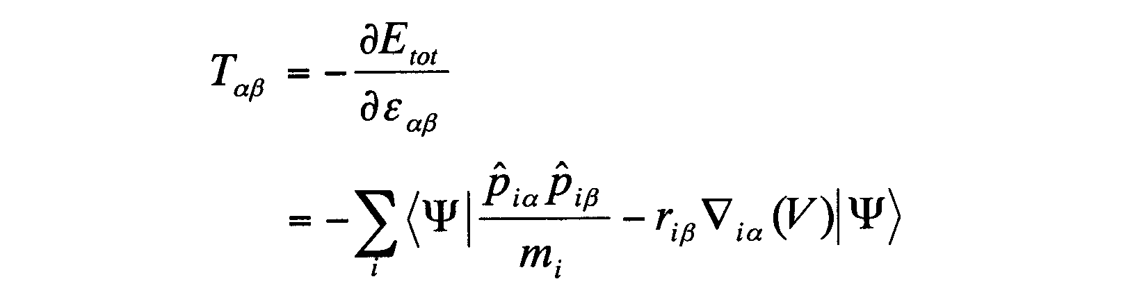
タイトバインディング法を用いる場合は、全エネルギーが数1で表すことができるので、応力は以下のようになる。

ここで、数5を用いると、

今、数5のSijが単位行列の場合を示した。
Rは歪みがある状況では、下記のように表すことができる。
Rは歪みがある状況では、下記のように表すことができる。

従って、

一方、

また、本情報処理装置は、物質の微小領域を平行六面体に置き換え、平行六面体をX、YおよびZ方向に無限に繰り返す構造を仮定する。平行六面体をX、YおよびZ方向に無限に繰り返す構造では、物質が均一であることが仮定できるので、平均を意味する<>は、単純に1個の平行六面体内での積分記号に変形できる。そこで、数10は、平行六面体内の応力を波動関数Ψで平均する式となっている。
数10で、波動関数Ψで平均される応力中の第1項、すなわち、運動量の演算子の積で示される第1項は、原子の運動エネルギーを1回微分した式である。この第1項は、原子の運動エネルギーから生じる圧力の項である。また、波動関数Ψで平均される応力中の第2項は、ポテンシャル、例えば、クーロン力等により生じる圧力の項である。
そして、平行六面体の周期構造を採用することで、並進ベクトルRを用いて周期構造を仮定した上での応力を求めることができる。また、波動関数Ψは、数3に示したように、原子軌道の和とすることができ、数3の係数は、数4、数5の形式で解くことができる。また、数5は、経験的パラメータを用いて、現実の物質の値と一致するように設定すればよい。したがって、数9によって、平行六面体の応力の平均値を求めることができる。
以上のように、微小領域を平行六面体に置き換え、無限に繰り返す構造を仮定することで、数9あるいは数10の応力の平均の式を、平行六面体内の積分に帰着できる。
以上のように、応力の平均値は、最終的には数14、数15の形で表すことができるので、HijやErepをRで微分し、固有値問題の解であるCi、Cjを用いることによって計算できる。
そして、数9の式で得られる平行六面体内の平均応力を物質の微小領域の応力とする。微小領域は、微小領域の中心座標、例えば、重心(Xi,Yi、Zi)と対応付けて、(Xi,Yi、Zi、Txxi,Txyi=Tyzi,Txzi=Tzxi,Tyyi,Tyzi=Tzyi,Tzzi)の形式で記憶装置のファイルに格納すればよい。したがって、図1に示したF3とF4とを微小領域の数だけ繰り返すことで、物質中の各微小領域中の応力を算出し、ファイルに格納できる。
図1のF6の処理において、各領域で求めた応力を線形補間することにより局所応力を求める。各微小領域で計算した応力の値は、平行六面体を形成する8原子の重心座標の値とする。そして、線形補間を行うことによって全空間における応力の関数(応力分布)を求める。
例えば、微小領域V1において、重心が(X1,Y1、Z1)であり、X軸方向の応力Tyz1が得られているとする。また、微小領域V1に隣接する微小領域V2の重心が(X1+D,Y1、Z1)であり、X軸方向の応力Tyz2が得られているとする。
この場合に、(X1,Y1、Z1)と(X1+D,Y1、Z1)との間のX軸方向の応力は、Txy(d)=((D-d)Txy1+dTxy2)/D;とすればよい。ここで、dは、微小領域V1の重心からの距離である。
以上述べたように、本情報処理装置は、経験的パラメータを用いた量子論に基づく計算手法において局所応力の計算および計算された応力の分布の計算を可能にする。したがって、求めることができる物理量の範囲を拡張することができる。
すなわち、本情報処理装置は、物質に含まれる原子の結晶構造を基準に、物質の原子構造を微小領域に分割する。そして、本情報処理装置は、分割によって得られた微小領域を平行六面体に置き換え、平行六面体の繰り返しによる仮想結晶構造を作成する。仮想結晶構造は、均一な物質と考えてよいので、本情報処理装置は、仮想結晶構造中の1つの平行六面体内の積分計算で、応力の平均値を求める。そして、本情報処理装置は、仮想結晶構造で得られた応力の平均値を物質の微小領域の応力とする。以上のような処理を繰り返すことで、本情報処理装置は、物質の原子構造のそれぞれの微小部分の応力を計算する。したがって、本情報処理装置は、物質中の応力分布、すなわち、局所応力を求めることができる。
以上のような手順において、本情報処理装置は、物質に含まれる原子の結晶構造を基準にして物質を微小部部分に分割するので、微小部分と微小部分の周囲の原子構造との関係を、極力本来の原子構造に類似させた状態で、仮想結晶構造を作成できる。したがって、仮想結晶構造から得られた平均応力は、物質中の微小部分に作用する応力に近いものと考えてよい。本情報処理装置は、以上のような物質本来の物理的性質を極力維持した状態で、仮想結晶構造による平均応力の計算を可能とする。
そして、本情報処理装置は、計算負荷が比較的少ない経験的パラメータを用いた量子論を用いるので、ナノデバイスの開発において、物質中の欠陥・亀裂の発生を原子レベルで理解するために重要な局所応力を、数千原子以上からなる実用的な規模の系について、実用的な時間で計算できるようになる。
さらに、以下の三点の特長を持つ。
(1)上記の計算は微小領域ごとに独立して行えるため、プロセッサの並列計算による高速化が容易である。(2)本発明による局所応力計算では、シミュレーションする物質を微小領域に分解するので、原子座標さえ与えられれば、計算負荷の重い経験的パラメータを用いない量子論に基づく計算手法を用いても、微小領域の応力を計算できるという特長を持つ。すなわち、応力計算の前提となる物質の原子構造あるいは原子の位置を求めるシミュレーションに制限はない。例えば、図2の処理以外の処理による原子構造に対しても、本情報処理装置は応力計算可能である。(3)必要な領域だけの局所応力計算が可能であり、要件に応じて計算コストを削減することができる。
(1)上記の計算は微小領域ごとに独立して行えるため、プロセッサの並列計算による高速化が容易である。(2)本発明による局所応力計算では、シミュレーションする物質を微小領域に分解するので、原子座標さえ与えられれば、計算負荷の重い経験的パラメータを用いない量子論に基づく計算手法を用いても、微小領域の応力を計算できるという特長を持つ。すなわち、応力計算の前提となる物質の原子構造あるいは原子の位置を求めるシミュレーションに制限はない。例えば、図2の処理以外の処理による原子構造に対しても、本情報処理装置は応力計算可能である。(3)必要な領域だけの局所応力計算が可能であり、要件に応じて計算コストを削減することができる。
図28および図29を参照して、実施例2に係る情報処理装置を説明する。図28は、実施例2に係る情報処理装置のハードウェア構成を例示する。本情報処理装置は、ネットワーク30に接続可能なコンピュータである。本情報処理装置は、CPU11、メモリ12、ハードディスクドライブ13等の外部記憶装置、ディスプレイ14、操作部15、通信部16、可搬型記憶媒体入出力装置17を有する。
CPU11は、メモリ12に実行可能に展開されたコンピュータプログラムを実行し、情報処理装置の機能を提供する。CPU11は、1個に限定されず、複数のコアを含むものでもよい。
メモリ12は、CPU11が実行するコンピュータプログラム、CPU11が処理するデータ等を記憶する。メモリ11は、不揮発性のROM(Read Only Memory)と、揮発性のDRAM(Dynamic Random Access Memory)とを含む。
ハードディスクドライブ13に駆動されるハードディスクには、メモリ12に展開されるコンピュータプログラム、あるいは、CPU11が処理するデータ等が格納される。ハードディスクドライブ13に代えて、フラッシュメモリ等、SSD(Solid State Drive)を用いてもよい。ハードディスクドライブ13、あるいは、SSD等の外部記憶装置は、インターフェース13Aを通じて、CPU21に接続される。
インターフェース13Aは、例えば、USB(Universal Serial Bus)、IDE(Integrated Drive Electronics)、SCSI(Small Computer System Interface)、FC(Fibre Channel)等のインターフェースである。
ディスプレイ14は、例えば、液晶ディスプレイ、エレクトロルミネッセンスパネル等である。ディスプレイ14は、インターフェース14Aを通じて、CPU21に接続される。インターフェース14Aは、例えば、VGA(Video Graphics Array)等のグラフィックスモジュール、DVI(Digital Visual Interface)等のインターフェースである。
操作部15は、キーボード、マウス、タッチパネル、静電パッド等の入力装置である。静電パッドは、平面パッドを指等でなぞるユーザ操作を検知し、ユーザ操作に応じてディスプレイ上のカーソルの位置と移動状態とを制御するために使用される装置である。例えば、平面パッド下の電極の静電容量の変化によって、ユーザの指の動きが検知される。操作部15は、インターフェース15Aを通じて、CPU11に接続される。インターフェース15Aは、例えば、USBのインターフェースである。
通信部16は、NIC(Network Interface Card)とも呼ばれる。通信部16は、例えば、LAN(Local Area Network)のインターフェースである。通信部16は、インターフェース16Aを通じて、CPU11に接続される。インターフェース16Aは、例えば、CPU11の内部バスに接続する拡張スロットである。
可搬型記憶装置17は、例えば、CD(Compact Disc)、DVD(Digital Versatile Disk)、ブルーレイディスク、フラッシュメモリカード等の入出力装置である。可搬型記憶装置17は、インターフェース17Aを通じて、CPU11に接続される。インターフェース17Aは、例えば、USB、SCSI等のインターフェースである。
なお、図28では、情報処理装置として、単独のコンピュータを例示した。しかし、情報処理装置は、複数のコンピュータが違いに連携し、処理を分担して実行する複数のコンピュータであってもよい。
図29に、実施例2に係る情報処理装置の機能構成を例示する。本情報処理装置は、ハードディスク等の外部記憶装置上に、結晶構造のデータベース24および物質の原子構造ファイル25を有する。結晶構造のデータベース24が結晶中の原子位置を含む原子構造を記憶する手段に相当する。物質の原子構造ファイル25が物質中の原子位置を含む原子構造を記憶する手段に相当する。
ただし、結晶構造のデータベース24および物質の原子構造ファイル25の少なくとも一方は、情報処理装置の外部記憶装置以外の装置、例えば、メモリ12にあってもよい。また、結晶構造のデータベース24および物質の原子構造ファイル25の少なくとも一方は、ネットワーク上の記憶装置、例えば、SAN(Storage Area Network)にあってもよい。また、結晶構造のデータベース24および物質の原子構造ファイル25の少なくとも一方は、ネットワークを通じて、アクセス可能なネットワーク上の他のコンピュータ、例えばデータベースサーバ上にあってもよい。
結晶構造のデータベース24のフォーマットは、実施例1の図15に示したものと同様である。また、物質の原子構造ファイル25は、実施例1で説明した経験的パラメータを用いた原子構造最適化処理、例えば、最急降下法や共役勾配法で求められる。ここで、物質の原子構造ファイル25は、例えば、原子種(ATYPEi)、原子のX座標(Xi)、Y座標(Yi)、Z座標(Zi)を含むレコードを多数含む。
そして、情報処理装置は、CPU11が、メモリ12に実行可能に展開されたプログラムを実行し、制御手段21、分割手段22および物質の分割部分平均応力算出手段23として機能する。
すなわち、分割手段22は、物質の原子構造ファイル25から物質の原子構造中に含まれる原子の位置を読み出す。そして、分割手段22は、物質を複数に分割した分割部分中の原子位置と原子を含む結晶中の原子位置とを比較する。そして、分割手段22は、物質を複数に分割した分割部分の原子位置と、当該物質の原子を含む結晶の原子位置とを比較し、分割部分と結晶との間で対応する原子間の相対距離の評価値が最も小さくなるように、分割部分の原子位置と結晶の原子位置とを対応付ける。このような分割部分の原子と、結晶構造中の原子との対応付けの手順は、実施例1において、図8において例示した処理と同様である。そして、分割手段22は、結晶の単位格子に相当する、物質の分割部分を特定する。ここで、分割部分は、例えば、実施例1でいう物質の微小部分に相当する。
平行六面体形成手段23は、分割手段22によって分割された物質の分割部分を取得する。分割部分は、例えば、六面体である。平行六面体形成手段23は、分割部分の頂点と平行六面体の頂点との間で相対距離の評価値が最も小さくなるような平行六面体を決定する。この場合の平行六面体形成手段23の処理手順は、実施例1に示した図18A-図24の処理と同様である。
平均応力算出手段24は、平行六面体形成手段23が作成した平行六面体を繰り返した仮想結晶構造を作成する。そして、平均応力算出手段24は、実施例1に示した式10と同様の計算式にしたがって、仮想結晶構造の平均応力を計算する。
制御手段21は、分割手段22、平行六面体形成手段23、および平均応力算出手段24を用いて、物質の原子構造ファイル25を処理する。すなわち、物質の原子構造ファイル25で付与される原子構造を分割部分に分割し、分割部分を平行六面体に変更し、仮想結晶構造を生成し、仮想結晶構造から得られる平均応力を当該分割部分の応力とする。制御手段21は、分割手段22、平行六面体形成手段23、および平均応力算出手段24を繰り返し実行することによって、物質の原子構造ファイル25で付与される原子構造で生じる応力分布を作成する。応力分布は、例えば、分割部分の重心(Xi,Yi,Zi)を用いて、(Xi,Yi,Zi,Txyi,Tyzi,Tzxi)のように表し、メモリ12に格納することができる。
なお、均応力算出手段24で得られる平均応力は、分割手段22で分割された分割部分に作用する応力、すなわち、分割部分と他の分割部分との境界面に作用するである。一方、分割部分と他の分割部分との境界面以外の位置の応力については、制御手段21は、境界面からの距離にしたがった線形補間によって求める。このようにして、制御手段21は、物質の原子構造ファイル25で付与される物質中の応力分布を出力する。図29では、省略されているが、応力分布の出力先は、例えば、外部記憶装置中のファイル、ディスプレイ14A、メモリ12中の他のアプリケーションプログラムの変数領域等である。
<コンピュータが読み取り可能な記録媒体>
コンピュータその他の機械、装置(以下、コンピュータ等)に上記いずれかの機能を実現させるプログラムをコンピュータ等が読み取り可能な記録媒体に記録することができる。そして、コンピュータ等に、この記録媒体のプログラムを読み込ませて実行させることにより、その機能を提供させることができる。
<コンピュータが読み取り可能な記録媒体>
コンピュータその他の機械、装置(以下、コンピュータ等)に上記いずれかの機能を実現させるプログラムをコンピュータ等が読み取り可能な記録媒体に記録することができる。そして、コンピュータ等に、この記録媒体のプログラムを読み込ませて実行させることにより、その機能を提供させることができる。
ここで、コンピュータ等が読み取り可能な記録媒体とは、データやプログラム等の情報を電気的、磁気的、光学的、機械的、または化学的作用によって蓄積し、コンピュータ等から読み取ることができる記録媒体をいう。このような記録媒体のうちコンピュータ等から取り外し可能なものとしては、例えばフレキシブルディスク、光磁気ディスク、CD-ROM、CD-R/W、DVD、ブルーレイディスク、DAT、8mmテープ、フラッシュメモリなどのメモリカード等がある。また、コンピュータ等に固定された記録媒体としてハードディスクやROM(リードオンリーメモリ)等がある。
本実施形態で説明した技術を用いることにより、新材料・デバイス開発において、物質中の欠陥・亀裂の発生を原子レベルで解明するができる。そのため、目的にあったデバイスの原子構造的な安定性を、実際に試作する前にシミュレーションを行うことによってある程度予測することができる。これは、開発時間と経費の削減、開発による環境負荷の低減につながる。本実施形態で説明した技術は、新材料・デバイス開発の技術分野、新材料・デバイス開発を支援する情報処理技術の分野に適用できる。
11 CPU
12 メモリ
21 制御手段
22 分割手段
23 平行六面体形成手段
24 物質の分割部分の平均応力算出手段
24 結晶構造のデータベース
25 物質の原子構造のファイル
12 メモリ
21 制御手段
22 分割手段
23 平行六面体形成手段
24 物質の分割部分の平均応力算出手段
24 結晶構造のデータベース
25 物質の原子構造のファイル
Claims (3)
- 物質中の原子位置を含む原子構造を記憶する手段と、
前記原子を含む結晶中の原子位置を含む原子構造を記憶する手段と、
前記物質を複数に分割した分割部分の原子位置と前記物質の原子を含む結晶の原子位置とを比較し、前記分割部分と前記結晶との間で対応する原子間の相対距離の評価値が最も小さくなるように、前記分割部分の原子位置と前記結晶の原子位置とを対応付け、前記結晶の単位格子に相当する、前記物質の分割部分を特定する分割手段と、
前記分割部分の頂点と平行六面体の頂点との間で相対距離の評価値が最も小さくなるような平行六面体を決定する平行六面体形成手段と、
前記平行六面体を繰り返した仮想結晶構造において前記平行六面体に加わる平均応力を算出する平均応力算出手段と、
前記分割手段、平行六面体形成手段、平均応力算出手段を繰り返し機能させることによって前記物質のそれぞれの分割部分の応力を特定する制御手段と、を備える情報処理装置。 - コンピュータが、物質中の原子位置を含む原子構造を記憶手段から読み出すステップと、
前記原子を含む結晶中の原子位置を含む原子構造を記憶手段から読み出すステップと、
前記物質を複数に分割した分割部分の原子位置と前記物質の原子を含む結晶の原子位置とを比較し、前記分割部分と前記結晶との間で対応する原子間の相対距離の評価値が最も小さくなるように、前記分割部分の原子位置と前記結晶の原子位置とを対応付け、前記結晶の単位格子に相当する、前記物質の分割部分を特定する分割ステップと、
前記分割部分の頂点と平行六面体の頂点との間で相対距離の評価値が最も小さくなるような平行六面体を決定する平行六面体形成ステップと、
前記平行六面体を繰り返した仮想結晶構造において前記平行六面体に加わる平均応力を算出する平均応力算出ステップと、
前記分割ステップ、平行六面体形成ステップ、および平均応力算出ステップを繰り返し実行することによって前記物質のそれぞれの分割部分の応力を特定する制御ステップと、を実行する情報処理方法。 - コンピュータに、物質中の原子位置を含む原子構造を記憶手段から読み出すステップと、
前記原子を含む結晶中の原子位置を含む原子構造を記憶手段から読み出すステップと、
前記物質を複数に分割した分割部分の原子位置と前記物質の原子を含む結晶の原子位置とを比較し、前記分割部分と前記結晶との間で対応する原子間の相対距離の評価値が最も小さくなるように、前記分割部分の原子位置と前記結晶の原子位置とを対応付け、前記結晶の単位格子に相当する、前記物質の分割部分を特定する分割ステップと、
前記分割部分の頂点と平行六面体の頂点との間で相対距離の評価値が最も小さくなるような平行六面体を決定する平行六面体形成ステップと、
前記平行六面体を繰り返した仮想結晶構造において前記平行六面体に加わる平均応力を算出する平均応力算出ステップと、
前記分割ステップ、平行六面体形成ステップ、および平均応力算出ステップを繰り返し実行することによって前記物質のそれぞれの分割部分の応力を特定する制御ステップと、を実行させることを特徴とするプログラム。
Priority Applications (3)
| Application Number | Priority Date | Filing Date | Title |
|---|---|---|---|
| PCT/JP2009/064470 WO2011021279A1 (ja) | 2009-08-18 | 2009-08-18 | 物質の応力を算出する情報処理装置 |
| JP2011527513A JP5338910B2 (ja) | 2009-08-18 | 2009-08-18 | 物質の応力を算出する情報処理装置 |
| US13/399,567 US20120150512A1 (en) | 2009-08-18 | 2012-02-17 | Information processing device for calculating stress of substance |
Applications Claiming Priority (1)
| Application Number | Priority Date | Filing Date | Title |
|---|---|---|---|
| PCT/JP2009/064470 WO2011021279A1 (ja) | 2009-08-18 | 2009-08-18 | 物質の応力を算出する情報処理装置 |
Related Child Applications (1)
| Application Number | Title | Priority Date | Filing Date |
|---|---|---|---|
| US13/399,567 Continuation US20120150512A1 (en) | 2009-08-18 | 2012-02-17 | Information processing device for calculating stress of substance |
Publications (1)
| Publication Number | Publication Date |
|---|---|
| WO2011021279A1 true WO2011021279A1 (ja) | 2011-02-24 |
Family
ID=43606744
Family Applications (1)
| Application Number | Title | Priority Date | Filing Date |
|---|---|---|---|
| PCT/JP2009/064470 Ceased WO2011021279A1 (ja) | 2009-08-18 | 2009-08-18 | 物質の応力を算出する情報処理装置 |
Country Status (3)
| Country | Link |
|---|---|
| US (1) | US20120150512A1 (ja) |
| JP (1) | JP5338910B2 (ja) |
| WO (1) | WO2011021279A1 (ja) |
Cited By (3)
| Publication number | Priority date | Publication date | Assignee | Title |
|---|---|---|---|---|
| JP2018152018A (ja) * | 2017-03-15 | 2018-09-27 | 日本電気株式会社 | 計算装置、計算方法、プログラム |
| US20220100931A1 (en) * | 2020-09-29 | 2022-03-31 | Robert Bosch Gmbh | Efficient scaling of neural-network interatomic potential prediction on cpu clusters |
| JPWO2022260178A1 (ja) * | 2021-06-11 | 2022-12-15 |
Families Citing this family (2)
| Publication number | Priority date | Publication date | Assignee | Title |
|---|---|---|---|---|
| US9858365B2 (en) * | 2013-10-24 | 2018-01-02 | Purdue Research Foundation | Physical modeling of electronic devices/systems |
| CN118974837A (zh) * | 2022-03-31 | 2024-11-15 | 松下知识产权经营株式会社 | 信息处理方法、信息处理系统以及程序 |
Citations (2)
| Publication number | Priority date | Publication date | Assignee | Title |
|---|---|---|---|---|
| JPH11120382A (ja) * | 1997-10-14 | 1999-04-30 | Internatl Business Mach Corp <Ibm> | メッシング方法及び装置 |
| JP2003347301A (ja) * | 2002-05-29 | 2003-12-05 | Fujitsu Ltd | 均質化法を用いた構造解析方法及び構造設計方法 |
Family Cites Families (3)
| Publication number | Priority date | Publication date | Assignee | Title |
|---|---|---|---|---|
| US6185472B1 (en) * | 1995-12-28 | 2001-02-06 | Kabushiki Kaisha Toshiba | Semiconductor device manufacturing method, manufacturing apparatus, simulation method and simulator |
| US6931812B1 (en) * | 2000-12-22 | 2005-08-23 | Stephen Leon Lipscomb | Web structure and method for making the same |
| EP1577822A1 (en) * | 2004-03-15 | 2005-09-21 | Avant-Garde Material Simulation SARL | Method for energy ranking of molecular crystals using DFT calculations and empirical van der Waals potentials |
-
2009
- 2009-08-18 JP JP2011527513A patent/JP5338910B2/ja not_active Expired - Fee Related
- 2009-08-18 WO PCT/JP2009/064470 patent/WO2011021279A1/ja not_active Ceased
-
2012
- 2012-02-17 US US13/399,567 patent/US20120150512A1/en not_active Abandoned
Patent Citations (2)
| Publication number | Priority date | Publication date | Assignee | Title |
|---|---|---|---|---|
| JPH11120382A (ja) * | 1997-10-14 | 1999-04-30 | Internatl Business Mach Corp <Ibm> | メッシング方法及び装置 |
| JP2003347301A (ja) * | 2002-05-29 | 2003-12-05 | Fujitsu Ltd | 均質化法を用いた構造解析方法及び構造設計方法 |
Cited By (6)
| Publication number | Priority date | Publication date | Assignee | Title |
|---|---|---|---|---|
| JP2018152018A (ja) * | 2017-03-15 | 2018-09-27 | 日本電気株式会社 | 計算装置、計算方法、プログラム |
| US10592815B2 (en) | 2017-03-15 | 2020-03-17 | Nec Corporation | Calculation apparatus, calculation method, and program |
| US20220100931A1 (en) * | 2020-09-29 | 2022-03-31 | Robert Bosch Gmbh | Efficient scaling of neural-network interatomic potential prediction on cpu clusters |
| US11815945B2 (en) * | 2020-09-29 | 2023-11-14 | Robert Bosch Gmbh | Efficient scaling of neural-network interatomic potential prediction on CPU clusters |
| JPWO2022260178A1 (ja) * | 2021-06-11 | 2022-12-15 | ||
| JP7403032B2 (ja) | 2021-06-11 | 2023-12-21 | 株式会社Preferred Networks | 訓練装置、推定装置、訓練方法、推定方法及びプログラム |
Also Published As
| Publication number | Publication date |
|---|---|
| US20120150512A1 (en) | 2012-06-14 |
| JP5338910B2 (ja) | 2013-11-13 |
| JPWO2011021279A1 (ja) | 2013-01-17 |
Similar Documents
| Publication | Publication Date | Title |
|---|---|---|
| Lim et al. | Granular element method for three‐dimensional discrete element calculations | |
| CN101147172B (zh) | 图像处理系统以及图像处理方法 | |
| Shimada et al. | Anisotropic triangular meshing of parametric surfaces via close packing of ellipsoidal bubbles | |
| Singh et al. | Orientation sampling for dictionary-based diffraction pattern indexing methods | |
| Donev et al. | A linear programming algorithm to test for jamming in hard-sphere packings | |
| JP5338910B2 (ja) | 物質の応力を算出する情報処理装置 | |
| EP3051446B1 (en) | Engraving a 2d image on a subdivision surface | |
| US20160188770A1 (en) | Simulating the machining of a workpiece | |
| Shimada et al. | Anisotropic triangulation of parametric surfaces via close packing of ellipsoids | |
| JPS61224078A (ja) | 有限要素を発生する方法 | |
| CN101493854A (zh) | 多目标最优化设计支持设备、方法和程序存储介质 | |
| Purwar et al. | On the effect of dual weights in computer aided design of rational motions | |
| Mollon | A numerical framework for discrete modelling of friction and wear using Voronoi polyhedrons | |
| JPWO2007086193A1 (ja) | 有限要素法による構造解析方法及びプログラム | |
| Benabbou et al. | Numerical modeling of nanostructured materials | |
| Burkhart et al. | Adaptive and feature‐preserving subdivision for high‐quality tetrahedral meshes | |
| Abu-Mualla et al. | A dataset generation framework for symmetry-induced mechanical metamaterials | |
| Lee et al. | Representing thermal vibrations and uncertainty in molecular surfaces | |
| US20160231706A1 (en) | System and method for generating occlusion-culled hologram at high speed using omnidirectional angular spectrum | |
| Yang et al. | An open source, geometry kernel based high-order element mesh generation tool | |
| JP2021110997A (ja) | シミュレーション方法、シミュレーション装置、及びプログラム | |
| Kraus et al. | Finite element formulations for 3D convex polyhedra in nonlinear continuum mechanics | |
| JP7525416B2 (ja) | 解析方法、解析装置、及びプログラム | |
| Bertin et al. | A spectral approach for discrete dislocation dynamics simulations of nanoindentation | |
| Azernikov et al. | A new volume warping method for surface reconstruction |
Legal Events
| Date | Code | Title | Description |
|---|---|---|---|
| 121 | Ep: the epo has been informed by wipo that ep was designated in this application |
Ref document number: 09848478 Country of ref document: EP Kind code of ref document: A1 |
|
| WWE | Wipo information: entry into national phase |
Ref document number: 2011527513 Country of ref document: JP |
|
| NENP | Non-entry into the national phase |
Ref country code: DE |
|
| 122 | Ep: pct application non-entry in european phase |
Ref document number: 09848478 Country of ref document: EP Kind code of ref document: A1 |