WO2011007693A1 - 融着接続構造およびその構造を有する光導波路素子、これを用いる光源装置、および接続方法 - Google Patents
融着接続構造およびその構造を有する光導波路素子、これを用いる光源装置、および接続方法 Download PDFInfo
- Publication number
- WO2011007693A1 WO2011007693A1 PCT/JP2010/061408 JP2010061408W WO2011007693A1 WO 2011007693 A1 WO2011007693 A1 WO 2011007693A1 JP 2010061408 W JP2010061408 W JP 2010061408W WO 2011007693 A1 WO2011007693 A1 WO 2011007693A1
- Authority
- WO
- WIPO (PCT)
- Prior art keywords
- optical waveguide
- fiber
- optical
- film
- light
- Prior art date
- Legal status (The legal status is an assumption and is not a legal conclusion. Google has not performed a legal analysis and makes no representation as to the accuracy of the status listed.)
- Ceased
Links
Images






Classifications
-
- G—PHYSICS
- G02—OPTICS
- G02B—OPTICAL ELEMENTS, SYSTEMS OR APPARATUS
- G02B6/00—Light guides; Structural details of arrangements comprising light guides and other optical elements, e.g. couplings
- G02B6/24—Coupling light guides
- G02B6/26—Optical coupling means
- G02B6/28—Optical coupling means having data bus means, i.e. plural waveguides interconnected and providing an inherently bidirectional system by mixing and splitting signals
- G02B6/293—Optical coupling means having data bus means, i.e. plural waveguides interconnected and providing an inherently bidirectional system by mixing and splitting signals with wavelength selective means
- G02B6/29346—Optical coupling means having data bus means, i.e. plural waveguides interconnected and providing an inherently bidirectional system by mixing and splitting signals with wavelength selective means operating by wave or beam interference
- G02B6/29361—Interference filters, e.g. multilayer coatings, thin film filters, dichroic splitters or mirrors based on multilayers, WDM filters
- G02B6/29368—Light guide comprising the filter, e.g. filter deposited on a fibre end
-
- G—PHYSICS
- G02—OPTICS
- G02B—OPTICAL ELEMENTS, SYSTEMS OR APPARATUS
- G02B6/00—Light guides; Structural details of arrangements comprising light guides and other optical elements, e.g. couplings
- G02B6/24—Coupling light guides
- G02B6/255—Splicing of light guides, e.g. by fusion or bonding
- G02B6/2551—Splicing of light guides, e.g. by fusion or bonding using thermal methods, e.g. fusion welding by arc discharge, laser beam, plasma torch
-
- H—ELECTRICITY
- H01—ELECTRIC ELEMENTS
- H01S—DEVICES USING THE PROCESS OF LIGHT AMPLIFICATION BY STIMULATED EMISSION OF RADIATION [LASER] TO AMPLIFY OR GENERATE LIGHT; DEVICES USING STIMULATED EMISSION OF ELECTROMAGNETIC RADIATION IN WAVE RANGES OTHER THAN OPTICAL
- H01S2301/00—Functional characteristics
- H01S2301/02—ASE (amplified spontaneous emission), noise; Reduction thereof
-
- H—ELECTRICITY
- H01—ELECTRIC ELEMENTS
- H01S—DEVICES USING THE PROCESS OF LIGHT AMPLIFICATION BY STIMULATED EMISSION OF RADIATION [LASER] TO AMPLIFY OR GENERATE LIGHT; DEVICES USING STIMULATED EMISSION OF ELECTROMAGNETIC RADIATION IN WAVE RANGES OTHER THAN OPTICAL
- H01S3/00—Lasers, i.e. devices using stimulated emission of electromagnetic radiation in the infrared, visible or ultraviolet wave range
- H01S3/05—Construction or shape of optical resonators; Accommodation of active medium therein; Shape of active medium
- H01S3/06—Construction or shape of active medium
- H01S3/063—Waveguide lasers, i.e. whereby the dimensions of the waveguide are of the order of the light wavelength
- H01S3/067—Fibre lasers
Definitions
- the present invention relates to an optical waveguide connection structure.
- an optical filter may be arranged by partially cutting the optical waveguide (Non-patent Document 1), It is necessary to align the coated optical waveguide and fix it to the substrate (Patent Document 1). Further, in order to suppress the return light of the reflected light generated at the filter insertion portion, a method has been proposed in which the filter is disposed obliquely with respect to the optical waveguide (Non-Patent Document 2). In the method of arranging the filter diagonally, the filter is fixed using an adhesive, which causes a problem in long-term stability. In particular, when light in the absorption wavelength band of the adhesive is handled, it is expected that the adhesive is significantly deteriorated by light.
- the light is once emitted into space, transmitted through the filter, and recombined with the optical waveguide.
- a method using a fiber Bragg grating (FBG), a method using a fiber coupler, and the like A method using a fiber Bragg grating (FBG), a method using a fiber coupler, and the like. Specifically, an example in which excitation light is guided or output by a fiber and combined with or separated from the laser light in a laser using a fiber-shaped amplification medium will be described with reference to FIGS.
- FBG fiber Bragg grating
- FIG. 1 shows an example in which a fiber laser device is configured by re-injecting pumping light output from a fiber from a semiconductor light source into a space through a lens to a rare earth-doped fiber that is an amplification medium.
- Excitation light from the semiconductor light source unit 101 is output from the output fiber unit 102 connected to the semiconductor light source unit 101, collimated by the collimator lens 103-a, transmitted through the excitation light transmission / laser light reflection mirror 104, and collimated.
- the light is collected by the lens 103-b and enters the rare earth-doped fiber 105.
- the incident excitation light is absorbed in the rare earth-doped fiber 105 and stimulated emission occurs, and the light generated thereby is disposed on the excitation light transmitting / laser light reflecting mirror 104 and on the opposite side of the rare earth-doped fiber 105 from the excitation light incident side.
- the laser beam partial transmission mirror 106 is repeatedly reflected and amplified, and a part thereof is emitted from the laser light partial transmission mirror 106 as laser light.
- the light emitted from the rare earth doped fiber 105 to the laser light partial transmission mirror 106 side is collimated by the collimating lens 103-c and enters the laser light partial transmission mirror 106.
- a wavelength selection film may be formed directly on the end face 105-a of the rare earth doped fiber 105 instead of using the mirror 104, but a lens is interposed between the output fiber 102 and the rare earth doped fiber 105. Inevitable.
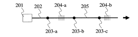
- FIG. 2 shows a method of forming a laser resonator in an optical waveguide by transmitting excitation light and reflecting laser light using FBG.
- the excitation light from the semiconductor light source unit 201 propagates through the output fiber unit 202 connected to the semiconductor light source unit 201 and is introduced into the FBG 204-a that is fusion-bonded (fusion-bonding point 203-a).
- the excitation light transmitted through the FBG 204-a is introduced into the rare earth doped fiber 205 that is fusion spliced (fusion splicing point 203-b).
- the introduced pumping light is absorbed in the rare earth-doped fiber 205 and stimulated emission occurs.
- the light generated thereby is fused and connected to the FBG 204-a and the rare earth-doped fiber 105 on the side opposite to the pumping light incident side.
- the reflection is repeatedly amplified with the FBG 204-b at the connection point 203-c), and a part thereof is transmitted through the FBG 204-b and emitted as laser light.
- excitation light or amplified light is not emitted from the fiber into the space during amplification, but there are four problems described below.
- the first point is that, generally, the reflection wavelength width of an FBG having a single-period refractive index change is narrow and 1 nm or less. Therefore, when giving a wide-band reflection characteristic to the FBG, the period of the refractive index change region is set. It is necessary to use a chirped FBG that has been chirped or a plurality of FBGs having different reflection wavelengths.
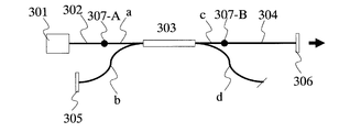
- FIG. 3 shows a method of configuring a laser resonator using a fiber coupler.
- Excitation light from the semiconductor light source unit 301 propagates through the output fiber unit 302 connected to the semiconductor light source unit 301, and is a fiber type WDM that is fusion spliced to the output fiber unit 302 (fusion splice point 307-A).
- the pump light is introduced into the input / output port a of the coupler 303 and output from the input / output port c.
- the pumping light output from the input / output port c is introduced into the rare earth doped fiber 304 that is fusion spliced to the input / output port c of the fiber type WDM coupler 303 (fusion splicing point 307-B).
- the introduced excitation light is absorbed in the rare earth doped fiber 304 and stimulated emission occurs, and the light generated thereby is installed on the end face of the input / output port b via the input / output ports c and b of the fiber type WDM coupler 303.
- Reflection is amplified repeatedly between the laser beam reflecting mirror 305 and the laser beam partial transmission mirror 306 provided on the opposite side of the rare earth-doped fiber 304 from the excitation light incident side, and a part of the reflection is amplified.
- the light passes through the mirror 306 and is emitted as laser light.
- the fiber type WDM coupler 303 When the fiber type WDM coupler 303 is configured using a fiber that is in a transverse single mode in the wavelength band used, the excitation light is transmitted between the input / output ports ac without loss, and the laser light is input / output port b ⁇ . It becomes possible to transmit between c without loss.
- the fiber type WDM coupler 303 when configured using a fiber that is multimode in the wavelength band used, the fiber propagation constant in the coupler varies from mode to mode, so all mode components are desired uniformly.
- the incident light passes through the fiber type WDM coupler 303, other than a specific mode component is coupled to another port, and loss occurs.
- lateral multimode excitation light not only couples the input / output ports from a to c, but also couples the input / output ports from a to d.
- the transverse multimode laser light not only couples the input / output port from c to b, but also partially couples the input / output port from c to a.
- the fiber type WDM when it is desired to introduce lateral multimode excitation light into the resonator, or when it is desired to construct a resonator capable of oscillation in the transverse multimode at the laser oscillation wavelength, the fiber type WDM is used. Couplers are unsuitable, and the laser characteristics are significantly degraded due to loss.
- An object of the present invention is to provide a connection structure that can suppress the influence of wavelength or mode of light propagating in an optical waveguide.
- one end face of the optical waveguide A is coated with an optical functional film, and one end face of the optical waveguide A coated with the optical functional film, and one piece of the optical waveguide B
- the present invention provides a fusion splicing structure that is fusion spliced with an end face facing each other.
- the optical waveguide A and the optical waveguide B are made of glass base materials having different glass transition temperatures, and the optical waveguide A is configured with a glass transition temperature of the glass base material constituting the optical waveguide B.
- the fusion splicing structure as described above, wherein the glass base material having a high glass transition temperature, or the optical waveguides of the optical waveguide A and the optical waveguide B are either step index type optical waveguides or graded index type optical waveguides
- the fusion splicing structure described above is provided.
- the optical functional film transmits or reflects light having a predetermined wavelength, light propagates from the optical waveguide A to the optical waveguide B, or from the optical waveguide B to the optical waveguide A.
- a non-reflective film for light propagating to the light a dispersion compensating film for compensating dispersion of light propagating through the optical waveguide A or light propagating through the optical waveguide B, light propagating through the optical waveguide A, or the optical waveguide B
- a fusion splicing structure which is a film having birefringent properties or a polarization separation film, a fluorescent film, a dielectric multilayer film, or a metal film that separates into different polarization components with respect to light propagating through the light It is.
- an optical waveguide device having the above-described fusion splicing structure is provided.
- the present invention provides a light source device in which at least one of the above-mentioned fusion splicing structure or optical waveguide element is disposed in an optical path, or wavelength selection in which the optical functional film reflects light of a predetermined wavelength.
- the present invention provides a laser device including the above-described optical waveguide element as a film and a laser resonator constituted by a fiber Bragg grating.
- the present invention is a method for connecting two optical waveguides, wherein one end surface of the optical waveguide A whose one end surface is coated with an optical functional film is opposed to one end surface of the optical waveguide B. And providing a connection method for fusion splicing.
- the optical functional film is a film that changes the transmittance, reflectance, light transmission spectrum, reflection spectrum, or polarization of light incident on the optical functional film. As such, light, electric field, magnetic field, heat and the like may be applied.
- membrane is not specifically limited, An organic material and an inorganic material may be sufficient, and a crystalline and amorphous state may be sufficient.
- the optical waveguide A, the film, and the optical waveguide B can be fixed without using an adhesive, a stable connection structure can be maintained over a long period of time.
- the light propagating through the optical waveguide is UV to visible light or in the case of a transverse multimode, it is possible to realize a light transmission characteristic or a reflection characteristic independent of the mode.
- An example of a structure of a fiber laser apparatus is shown.
- An example of the structure of the laser resonator using FBG is shown.
- 1 shows an example of the configuration of a laser resonator using a fiber coupler.
- the cross section of the form before comprising the fusion splicing structure of this invention is shown.
- the cross section of an example of the fusion splicing structure of this invention is shown.
- the outline of the section of the composition before connection in an example is shown.
- the outline of the section of the fusion splicing structure of Examples 1 and 2 is shown.
- 1 shows a measurement system for a fusion spliced structure.
- permeability spectrum of Example 1 is shown.
- 4 shows an outline of a cross section of a fiber laser of Example 3.
- the laser oscillation spectrum of Example 3 is shown.
- 4 shows an outline of a cross section of a fiber laser of Example 4.
- the laser oscillation spectrum of Example 4 is shown. 2 shows an outline
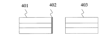
- FIG. 4 shows a form before the fusion splicing structure of the present invention is configured.
- the fiber 401 and the fiber 403 are fibers having different glass compositions, and the glass transition temperature of the fiber 403 is higher than the glass transition temperature of the fiber 401.
- An optical functional film 402 that transmits light having a desired wavelength ⁇ 1 and reflects light having a desired wavelength ⁇ 2 is provided in advance on the end face of the fiber 401 having a higher glass transition temperature.
- FIG. 5 shows a fusion spliced structure in which the connection surface between the fiber 401 and the fiber 403 is fusion-bonded by heating to a temperature at which only the fiber 403 is softened.
- the fusion splicing structure shown in FIG. 5 constitutes an optical waveguide element composed of the fibers 401 and 403 and the optical functional film 402.
- quartz glass having a glass transition temperature of 1000 ° C. or higher is desirable, but not limited thereto.
- halide glass vanadium glass, bismuth glass, and chalcogenite glass are preferable, but not limited thereto, and a plastic material is also used. be able to.
- the glass transition temperature of the fiber 401 and the fiber 403 may be the same, or the same kind of material may be used. In this case, it is necessary to reduce the heat applied to the optical functional film 402 applied to the end face of the fiber 401 as much as possible. Therefore, when performing fusion splicing, the fiber 401 provided with the optical functional film 402 is not heated, and only the fiber 403 is heated to the glass transition temperature or higher, and immediately after that, the optical functional film of the fiber 401 is heated. What is necessary is just to carry out the fusion
- the optical functional film 402 is a light transmittance control film that transmits a part of light having a desired wavelength and reflects the rest, and a wavelength selection film in which an arbitrary wavelength dependency is given to the transmittance or the reflectance.
- Non-reflective coating film that suppresses Fresnel reflection, dispersion compensation film that controls dispersion of light generated by reflection, film that absorbs light guided in the optical waveguide and emits fluorescence, dielectric multilayer film, or metal You may be comprised by the film
- the optical functional film 402 may have a plurality of functions described above.
- the fiber 401 and the fiber 403 may be each independently a step index optical waveguide, a graded index optical waveguide, a GRIN lens, or a polarization maintaining optical waveguide. Further, the fiber 401 and the fiber 403 may be independently a multimode fiber or a single mode fiber. Further, the core of the optical waveguide of the fiber 401 or the fiber 403 is not limited to one, and may be a multi-core optical waveguide including a plurality of cores.
- the optical functional film is directly formed in the fusion splicing structure without passing through a space, so that reflection / transmission characteristics (or wavelength separation characteristics), such as a fiber coupler, are obtained. Is independent of the propagation mode. Moreover, since no adhesive is used for connection, there is little possibility of adhesive deterioration, and a stable connection structure can be maintained over a long period of time.
- the fusion structure of the present invention can also be used for a light source device such as an ASE light source, a laser device, or a wavelength tunable light source.
- a light source device such as an ASE light source, a laser device, or a wavelength tunable light source.
- the fusion structure according to the present invention is disposed in an optical path between an excitation light source and an optical amplification fiber (such as a rare earth-doped fiber) excited by the pump light source, and emitted from the rare earth-doped fiber. It can be used to reflect the light that travels toward the excitation light source in the ASE light.
- an optical amplification fiber such as a rare earth-doped fiber
- a laser device When used in a laser device, for example, it can be used by constructing a laser resonator using two fusion structures according to the present invention, and the fusion structure according to the present invention and a normal reflection structure (for example, FBG, fiber) And a laser resonator using a loop mirror or the like.
- a wavelength tunable light source can be configured by disposing an etalon in the above-mentioned resonator to limit the oscillation wavelength or disposing a dispersion compensation element (prism, grating) or the like.
- a polarization controller or the like may be further disposed in the laser resonator.
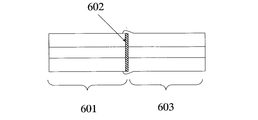
- Fig. 6 shows the outline of the configuration before connection.
- a quartz fiber 601 cleaved at right angles (NA 0.22, core diameter 4.0 ⁇ m, cladding diameter 125 ⁇ m, glass transition temperature> 1000 ° C.), and dielectric multilayer film 602 coated on the end face of the quartz fiber 601 ( And a fluoride fiber 603 (composition: ZBLAN, NA 0.22, core diameter 4.0 ⁇ m, cladding diameter 125 ⁇ m, glass transition temperature 280 ° C.).
- the quartz fiber 601 and the fluoride fiber 603 are both multimode fibers in the wavelength range of 400 to 550 nm.
- the quartz fiber 601 having the end face coated with the dielectric multilayer film 602 was heated to about 350 ° C. and then pressed against the fluoride fiber 603 to be fusion spliced to obtain a fusion spliced structure.
- FIG. 7 shows a schematic view of the fusion spliced shape of the obtained fusion spliced structure.
- the quartz fiber 601 was not deformed, and only the fluoride fiber 603 heated to the glass transition temperature or higher was deformed.
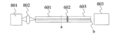
- FIG. 8 shows a measurement system for measuring the wavelength transmittance of the obtained fusion spliced structure.
- the measurement system shown in FIG. 8 includes a halogen lamp 801, a condenser lens 802, and an optical spectrum analyzer 803 (ANDO AQ6315-A).
- Light emitted from the halogen lamp 801 is obtained by the condenser lens 802.
- Light which is introduced by being condensed on the core portion of the end surface on the quartz fiber 601 side of the fusion spliced structure is introduced into the optical spectrum analyzer 803.
- the measurement is performed by measuring the spectrum of light emitted from the end surface b on the fluoride fiber 603 side of the obtained fusion spliced structure, and then cleaving the quartz fiber 601 part of the obtained fusion spliced structure.
- the spectrum of the light emitted from the end face a obtained by removing the fluoride fiber 603 side was measured.
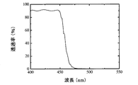
- FIG. 9 shows a transmittance spectrum obtained by calculating the ratio of the measured spectral intensities of the end face a and the end face b.
- the transmissivity of the fusion splicing part is 90% at a wavelength of 400 to 455 nm, and ⁇ 1% at a wavelength of 470 to 550 nm, indicating that it has a wavelength selection function.
- Both the quartz fiber 601 and the fluoride fiber 603 used are the same as in Example 1 except that both are single mode fibers at a wavelength of 400 to 550 nm. That is, as shown in FIG. 6, a quartz fiber 601 (NA 0.13, core diameter 2.2 ⁇ m, cladding diameter 125 ⁇ m, glass transition temperature> 1000 ° C.) cleaved at right angles, and dielectric multilayer coated on the end face of the quartz fiber 601 A film 602 (wavelength 400 to 455 nm transmission, wavelength 470 to 550 nm reflection), and a fluoride fiber 603 (composition: ZBLAN, NA 0.13, core diameter 2.2 ⁇ m, cladding diameter 125 ⁇ m, glass transition temperature 280 ° C.) .
- the fusion spliced structure was obtained by fusion splicing, and the wavelength transmittance of the obtained spliced connection structure was measured.
- the transmittance of the fusion spliced portion was a transmittance> 93% at a wavelength of 400 to 455 nm, and a transmittance ⁇ 1% at a wavelength of 470 to 550 nm.
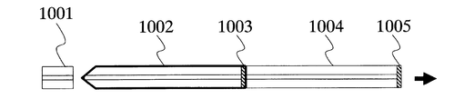
- FIG. 10 shows an example in which the present invention is applied to a fiber laser.
- the fiber laser shown in FIG. 10 includes a GaN laser diode 1001 (wavelength 448 nm) and a quartz fiber 1002 (NA 0.22 having a lens processed at one end).
- the quartz fiber 1002 and the Pr 3+ doped fluoride fiber 1004 are both multimode fibers in the wavelength range of 400 to 550 nm.
- Light emitted from the GaN laser diode 1001 is introduced from one end of the quartz fiber 1002 that has been processed into a lens by being coupled to the core by a lens shape.
- the quartz fiber 1002 and the Pr 3+ doped fluoride fiber 1004 are fusion-bonded in the same manner as in Example 1, and the emitted light (excitation light) of the GaN laser diode 1001 introduced into the quartz fiber 1002 is a dielectric multilayer. It passes through the membrane 1003 without loss and excites Pr 3+ ions in the Pr 3+ doped fluoride fiber 1004.
- the light emission obtained by the Pr 3+ doped fluoride fiber 1004 oscillates by reciprocating the resonator constituted by the dielectric multilayer films 1003 and 1005.
- the optical spectrum of the laser beam output from the dielectric multilayer film 1005 was measured with an optical spectrum analyzer (not shown).
- FIG. 11 shows an optical spectrum of the laser beam output when excitation light 250 mW is introduced into the quartz fiber 1002.
- broadband laser oscillation could be confirmed in the wavelength range of 519.6 to 521.9 nm.
- a laser resonator can be configured without a space.
- both ends of a fiber as a laser medium are directly coated with a reflection film.
- a laser resonator is configured using FBG or the like, the laser output is lowered because a fusion point that causes a loss is arranged inside the resonator.
- the connection mismatching portion is arranged outside the resonator, the loss of the laser resonator is small, and as a result, a high-power laser configuration is obtained.
- the quartz fiber 1002 having a lens processed at one end is used, and the laser having the simplest configuration is obtained. Since the lens processing portion of the quartz fiber 1002 is spherical, it is difficult to form a resonator mirror at the tip of the lens processing portion. Therefore, the arrangement of the resonator mirrors in the laser shown in this embodiment is most ideal. Further, instead of directly forming the dielectric multilayer film 1005 on the end face of the fluoride fiber 1004, after forming the dielectric multilayer film 1005 on the end face of another quartz fiber, the film-formed face is formed on the end face of the fluoride fiber 1004. It may be fusion-bonded to the emission side end face.
- FIG. 12 shows a fiber laser composed of FBG which is a reflection structure different from the fusion structure according to the present invention.
- the fiber laser shown in FIG. 12 has a GaN laser diode 1201 (wavelength 448 nm), a quartz fiber 1202 with a lens processed at one end (NA 0.22, core diameter 4.0 ⁇ m, cladding diameter 125 ⁇ m), and a quartz fiber 1202 lens processed.
- Dielectric multilayer 1203 (wavelength 400 to 455 nm transmitted, wavelength 470 to 550 nm reflected), Pr 3+ doped fluoride fiber 1204 (Pr 3+ doped concentration: 3000 ppm, NA 0.22, core diameter 4) 0.0 ⁇ m, clad diameter 125 ⁇ m, glass transition temperature 280 ° C.), FBG 1205 (fiber parameters are the same as quartz fiber 1202, FBG reflectivity is 85%, reflection center wavelength is 516.2 nm, 3 dB bandwidth is 0.2 nm) Composed. Note that the quartz fiber 1202, the Pr 3+ doped fluoride fiber 1204, and the FBG 1205 are multimode fibers in the wavelength range of 400 to 550 nm.
- the light emitted from the GaN laser diode 1201 is introduced from one end of the quartz fiber 1202 that has been processed into a lens by being coupled to the core by a lens shape.
- the quartz fiber 1202 and the Pr 3+ doped fluoride fiber 1204 are fused and connected in the same manner as in the first embodiment, and the emitted light (excitation light) of the GaN laser diode 1201 introduced into the quartz fiber 1202 is a dielectric multilayer. It passes through the membrane 1203 without loss and excites Pr 3+ ions in the Pr 3+ doped fluoride fiber 1204.
- the Pr 3+ doped fluoride fiber 1204 and the FBG 1205 are fusion-spliced, and the light emitted from the Pr 3+ doped fluoride fiber 1204 reciprocates through the resonator formed by the dielectric multilayer film 1203 and the FBG 1205. Cause laser oscillation.
- the optical spectrum of the laser beam output from the FBG 1205 was measured with an optical spectrum analyzer (not shown).
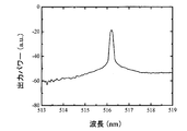
- FIG. 13 shows the optical spectrum of the laser beam output when the excitation light 250 mW is introduced into the quartz fiber 1202. As shown in FIG. 13, laser oscillation could be confirmed at the center wavelength of 516.2 nm. As described above, by using the connection structure according to the present invention, a laser resonator can be configured without a space.
- FIG. 14 A fiber laser when connected using an adhesive is shown in FIG. 14 includes a GaN laser diode 1401 (wavelength 448 nm), a quartz fiber 1402 (NA 0.22, core diameter 4.0 ⁇ m, clad diameter 125 ⁇ m) having a lens processed at one end, and a Pr 3+ doped fluoride fiber.
- Both the quartz fiber 1402 and the Pr 3+ doped fluoride fiber 1404 are multimode fibers in the wavelength range of 400 to 550 nm.
- the end face on which the lens is not processed is fixed in the ferrule 1406 and polished at a right angle, and then a dielectric multilayer film 1403 (wavelength 400 to 455 nm transmission, wavelength 470 to 550 nm reflection) is formed.
- a dielectric multilayer film 1403 wavelength 400 to 455 nm transmission, wavelength 470 to 550 nm reflection
- one surface of the fluoride fiber 1404 is coated with a dielectric multilayer film 1405 (transmittance of 15% at a wavelength of 521 ⁇ 10 nm).
- the present invention can be used in a field using an optical waveguide, such as an ASE light source, a laser device, or a light source device such as a wavelength variable light source, optical communication, a laser display, or an inspection device.
- an optical waveguide such as an ASE light source, a laser device, or a light source device such as a wavelength variable light source, optical communication, a laser display, or an inspection device.
Landscapes
- Physics & Mathematics (AREA)
- General Physics & Mathematics (AREA)
- Optics & Photonics (AREA)
- Engineering & Computer Science (AREA)
- Plasma & Fusion (AREA)
- Lasers (AREA)
- Optical Couplings Of Light Guides (AREA)
- Semiconductor Lasers (AREA)
- Mechanical Coupling Of Light Guides (AREA)
Abstract
【課題】本発明の目的は、光導波路中を伝搬する光の、波長またはモードの影響を抑制できる接続構造を提供することである。 【解決手段】接着剤を使用せず、膜がコーティングされた光導波路の端面と他の光導波路の端面とを融着接続できることを見出した発明で、2つの光導波路の接続において、光導波路Aの片端面に光機能性膜がコーティングされ、かつ、該光機能性膜がコーティングされている光導波路Aの片端面と、光導波路Bの片端面とを対向させて融着接続されている融着接続構造、またはこれを用いた光導波路素子。
Description
本発明は、光導波路の接続構造に関するものである。
複数波長の光が伝搬している光導波路において、特定波長の光のみを反射または透過させる場合には、光導波路を一部切断して光フィルタを配置したり(非特許文献1)、端面にコーティングされた光導波路をアライメントして基板に固定したり(特許文献1)する必要があった。また、フィルタ挿入部で生じた反射光の戻り光を抑制する場合には、光導波路に対して斜めにフィルタを配置させる方法が提案されてきた(非特許文献2)。フィルタを斜めに配置する方法では、接着剤を用いてフィルタを固定するため、長期安定性に問題があった。特に、接着剤の吸収波長帯の光を扱う場合には、光による接着剤の著しい劣化が生ずることが予想される。
また、光導波路を伝搬している光のうち、特定波長の光のみを反射、透過、または分離させる他の方法として、光を一度空間に出射させてフィルタを透過させ、光導波路に再結合させる方法、ファイバブラッググレーティング(FBG)を用いる方法、ファイバ型カプラを用いる方法などがある。具体的には、ファイバ形状の増幅媒体を用いるレーザにおいて励起光をファイバにより導波または出力しレーザ光との合波または分離する例を、図1~図3を用いて説明する。
図1では、半導体光源よりファイバから空間に出力された励起光を、レンズを介して増幅媒質である希土類添加ファイバへ再入射させてファイバレーザ装置を構成する例を示している。半導体光源部101からの励起光は、半導体光源部101に接続されている出力ファイバ部102より出力され、コリメートレンズ103-aでコリメートされ、励起光透過/レーザ光反射ミラー104を透過し、コリメートレンズ103-bで集光され希土類添加ファイバ105に入射される。入射した励起光が希土類添加ファイバ105中で吸収され誘導放出が起こり、これにより発生する光は、励起光透過/レーザ光反射ミラー104と、希土類添加ファイバ105の励起光入射側と反対側に設置されるレーザ光部分透過ミラー106との間で反射を繰り返し増幅され、その一部がレーザ光部分透過ミラー106からレーザ光として放出される。希土類添加ファイバ105よりレーザ光部分透過ミラー106側に放出する光は、コリメートレンズ103-cでコリメートされレーザ光部分透過ミラー106に入射する。このように、ファイバから空間に出力された励起光をミラーに通過させ、増幅媒質である希土類添加ファイバへ再入射させる場合、構成する部品の数が多く光学系が複雑になってしまう。構成部品を減らすために、ミラー104を用いる代わりに、希土類添加ファイバ105の端面105-aに直接波長選択膜を形成しても良いが、出力ファイバ102および希土類添加ファイバ105の間にレンズを介してしまうことは避けられない。
図2では、FBGを用いて、励起光を透過し、レーザ光を反射させることにより、光導波路中でレーザ共振器を構成する方法を示している。半導体光源部201からの励起光は、半導体光源部201に接続されている出力ファイバ部202を伝搬し、融着接続(融着接続点203-a)されているFBG204-aに導入される。FBG204-aを透過した励起光は、融着接続(融着接続点203-b)されている希土類添加ファイバ205に導入される。導入された励起光が希土類添加ファイバ205中で吸収され誘導放出が起こり、これにより発生する光は、FBG204-aと、希土類添加ファイバ105の励起光入射側と反対側に融着接続(融着接続点203-c)されているFBG204-bとの間で反射を繰り返し増幅され、その一部がFBG204-bを透過してレーザ光として放出される。
FBGを用いる場合、上記図1の例と異なり、増幅の過程で、励起光または増幅光がファイバから空間に放出されないが、下記に記載する4つの問題点がある。
第1点は、一般に単一周期の屈折率変化を有するFBGの反射波長幅は狭く、1nm以下であることから、FBGに広帯域な反射特性を付与する場合には、屈折率変化領域の周期をチャ-プさせたチャ-プドFBG、または異なる反射波長をもつ複数本のFBGを繋げて、用いる必要がある。
第2点は、FBGは、ファイバの渦中にゲルマニウムなどの添加物が添加されているため、FBG中を伝搬させる所望の光の波長が短いほど、添加物による吸収損失の影響が大きくなる。現在、UV~可視光領域専用のファイバとして、ファイバのコア部に純粋石英を用いた純粋石英コアファイバが市販されているが、このコア中には添加物が存在しない為、純粋石英コアファイバを用いてグレーティングを作製することは不可能である。したがって、FBGを特にUV光に対して使用することは困難である。
第3点は、マルチモードファイバを用いてFBGを作製する場合、モード毎にファイバ中の伝搬定数が異なるため、全ての伝搬モードに対して一様な反射率をもつFBGを構成することは困難である。
第4点は、増幅媒質である希土類添加ファイバのコア径を変える場合に、コア径度に希土類添加ファイバに接続するFBGを作製する必要があるため、手間がかかる。
図3では、ファイバカプラを用いてレーザ共振器を構成する方法を示している。半導体光源部301からの励起光は、半導体光源部301に接続されている出力ファイバ部302を伝搬し、出力ファイバ部302に融着接続(融着接続点307-A)されているファイバ型WDMカプラ303の励起光の入出力ポートaに導入され、入出力ポートcから出力される。入出力ポートcから出力された励起光は、ファイバ型WDMカプラ303の入出力ポートcに融着接続(融着接続点307-B)されている希土類添加ファイバ304に導入される。導入された励起光が希土類添加ファイバ304中で吸収され誘導放出が起こり、これにより発生する光は、ファイバ型WDMカプラ303の入出力ポートc、bを介して入出力ポートbの端面に設置されているレーザ光反射ミラー305と、希土類添加ファイバ304の励起光入射側と反対側に設置されているレーザ光部分透過ミラー306との間で反射を繰り返し増幅され、その一部がレーザ光部分透過ミラー306を透過してレーザ光として放出される。
ファイバ型WDMカプラ303が使用する波長帯で横シングルモードとなるファイバを用いて構成されている場合、励起光は入出力ポートa-c間を損失無く透過し、レーザ光は入出力ポートb-c間を損失無く透過することが可能となる。
しかし、ファイバ型WDMカプラ303が使用する波長帯でマルチモードとなるファイバを用いて構成されている場合、カプラ内でファイバの伝搬定数はモード毎に異なるため、全てのモード成分を一様に所望のポートへ結合させることが不可能となり、入射した光がファイバ型WDMカプラ303を通過する際に、特定のモード成分以外は他ポートに結合され損失が発生する。例えば、横マルチモードの励起光は入出力ポートをaからcに結合するだけでなく、一部は入出力ポートをaからdにも結合する。また、横マルチモードのレーザ光は入出力ポートをcからbに結合するだけでなく、一部は入出力ポートをcからaにも結合する。
したがって上記図3の例では、横マルチモードの励起光を共振器中に導入したい場合や、レーザ発振波長において、横マルチモードで発振が可能な共振器を構成したい場合などには、ファイバ型WDMカプラは不向きであり、損失のためにレーザの特性を著しく劣化させてしまう。
光通信技術の最新資料集V、80ページ、平成13年、オプトロニクス社
光ファイバとファイバ型デバイス、川上他著、222ページ、1996年、培風館
以上のように、光導波路を伝搬している光のうち、特定波長の光のみを反射、透過、または分離させる場合、特定波長の光損失を抑制するため、光導波路を伝搬する光を空間に放出せず光導波路中で特定波長の光のみを反射、透過、または分離させる方法が提案されている。例えば、フィルタを光導波路端面に接着剤を用いて接続する方法、増幅媒体をFBGまたはファイバ型WDMカプラに接続する方法がある。従来の方法では、接着剤を使用するため長期安定性に問題や、または、UV~可視光領域またはマルチモード光での使用が困難である為、使用できる光の波長やモードに制限が生じる問題がある。
本発明では、光導波路中を伝搬する光の、波長またはモードの影響を抑制できる接続構造を提供することを目的としている。
本発明者らは、鋭意検討を重ねた結果、接着剤を使用せず、膜がコーティングされた光導波路の端面と他の光導波路の端面とを融着接続できることを見出し、本発明に到ったものである。
すなわち、2つの光導波路の接続において、光導波路Aの片端面に光機能性膜がコーティングされ、かつ、該光機能性膜がコーティングされている光導波路Aの片端面と、光導波路Bの片端面とを対向させて融着接続されている融着接続構造を提供するものである。
さらには、該光導波路Aと該光導波路Bが、ガラス転移温度が異なるガラス母材により構成されており、かつ、光導波路Bを構成するガラス母材のガラス転移温度よりも光導波路Aを構成するガラス母材のガラス転移温度が高い前記記載の融着接続構造、または、該光導波路Aと該光導波路Bの光導波路が共に、ステップインデックス型光導波路またはグレーデットインデックス型光導波路のいずれか一方である上記記載の融着接続構造を提供するものである。
また本発明は、該光機能性膜が、所定の波長の光を透過または反射する波長選択膜、該光導波路Aから該光導波路Bに伝搬する光、または該光導波路Bから該光導波路Aに伝搬する光に対して無反射膜、該光導波路Aを伝搬する光または該光導波路Bを伝搬する光の分散を補償する分散補償膜、該光導波路Aを伝搬する光または該光導波路Bを伝搬する光に対して、複屈折の性質を有する膜または異なる偏波成分に分離する偏波分離膜、蛍光膜、誘電体多層膜、または金属膜である、融着接続構造を提供するものである。または、上記の融着接続構造を有する光導波路素子を提供するものである。
さらに本発明は、上記の融着接続構造または光導波路素子が、少なくとも1つ以上、光路中に配置されている光源装置、または、該光機能性膜が所定の波長の光を反射する波長選択膜である上記の光導波路素子と、ファイバブラッググレーティングにより構成されるレーザ共振器を含むレーザ装置、を提供するものである。
また本発明は、2つの光導波路の接続方法であって、片端面に光機能性膜がコーティングされている光導波路Aのコーティングされている片端面と、光導波路Bの片端面とを対向させて融着接続する、接続方法を提供するものである。
ここで、光機能性膜とは、該光機能性膜に入射する光に対し、その透過率、反射率、光の透過スペクトル、反射スペクトル、または偏光等に変化を与える膜であり、外部刺激として、光、電場、磁場、熱等が加えられてもよい。また、膜を構成する材料は、特に限定されず、有機材料、無機材料でもよく、また、結晶、アモルファスの状態であってもよい。
本発明により、接着剤を用いることなく、光導波路Aと膜、および光導波路Bを固定することができるため、長期にわたって安定な接続構造が維持できる。また、光導波路を伝搬する光がUV~可視光である場合や横マルチモードである場合にも、モードに依存しない光透過特性または反射特性を実現することができる。
本発明における実施形態の例を、図4、図5を用いて示す。図4は本発明の融着接続構造を構成する前の形態を示しており、ファイバ401およびファイバ403はガラス組成の異なるファイバであり、ファイバ403のガラス転移温度はファイバ401のガラス転移温度よりも低い。ガラス転移温度が高い方のファイバ401の端面には、所望の波長λ1の光を透過して所望の波長λ2の光を反射する光機能性膜402が予め施されている。さらに、ファイバ401とファイバ403の接続面を、ファイバ403のみが軟化する温度に過熱して融着接続した融着接続構造を図5に示す。図5に示す融着接続構造は、ファイバ401とファイバ403、および光機能性膜402による光導波路素子を構成している。
ガラス転移温度が高い方の光導波路を構成する母材としては、ガラス転移温度が1000℃以上である、石英系ガラスが望ましいが、この限りではない。
また、ガラス転移温度が低い方の光導波路を構成する母材としては、ハロゲン化物ガラス、バナジウム系ガラス、ビスマス系ガラス、カルコゲナイトガラスが望ましいが、この限りではなく、プラスチック製の材料も用いることができる。
また、ファイバ401とファイバ403のガラス転移温度は同一でも良く、さらには同種の材料であっても良い。この場合にはファイバ401の端面に施されている光機能性膜402に加わる熱を可能な限り少なくする必要がある。そのため、融着接続を行う場合には、光機能性膜402が施されているファイバ401は加熱せず、ファイバ403のみをガラス転移温度以上に加熱し、その直後にファイバ401の光機能性膜402が施されている面とファイバ403を押し当てることにより、融着接続すればよい。押し当てた直後、ファイバ403の端面は急激に冷却されるため、光機能性膜402への熱の影響を抑制することができる。
ここで、光機能性膜402は、所望の波長の光の一部を透過し、残りを反射する光透過率制御膜、透過率または反射率に任意の波長依存性が付与された波長選択膜、フレネル反射を抑制する無反射コーティング膜、反射により生じた光の分散を制御する分散補償膜、光導波路中を導波されている光を吸収し蛍光を発する膜、誘電体多層膜、または金属膜などにより構成されていても良い。また、光機能性膜402は、上記の複数の機能を兼ね備えても良い。
ファイバ401とファイバ403は、それぞれ独立して、ステップインデックス型光導波路、グレーデットインデックス型光導波路、またはGRINレンズであっても良く、偏波保持型の光導波路であっても良い。また、ファイバ401とファイバ403は、それぞれ独立して、マルチモードファイバまたはシングルモードファイバであってもよい。また、ファイバ401またはファイバ403の光導波路のコアは1つに限定されず、複数のコアを含むマルチコア光導波路であってもよい。
本発明の融着接続構造は、融着接続構造中に光機能性膜が空間を経由することなく直接形成されているので、ファイバカプラなどのように、反射/透過特性(または波長分離特性)が伝搬モードに依存しない。また、接続に接着剤を使用していないため、接着剤劣化の可能性が少なく、長期にわたって安定な接続構造が維持できる。
また、本発明の融着構造は、ASE光源、レーザ装置、または波長可変光源などの光源装置に利用することもできる。ASE光源に利用する場合には、例えば、本発明による融着構造を励起光源とこれにより励起される光増幅ファイバ(希土類添加ファイバなど)の中間にある光路中に配置し、希土類添加ファイバから発せられたASE光の内、励起光源側に進行する光を反射させるために利用できる。レーザ装置に利用する場合には、例えば、本発明による融着構造を2つ用いてレーザ共振器を構成することにより利用できるし、本発明の融着構造と通常の反射構造(例えばFBG、ファイバループミラー等)とを用いてレーザ共振器を構成することにより利用できる。さらには、上述の共振器中にエタロンを配置して発振波長を制限したり、または分散補償素子(プリズム、グレーティング)などを配置したりして、波長可変光源を構成できる。またレーザ発振をより安定化させるために、レーザ共振器中に偏波コントローラ等をさらに配置してもよい。
以下、実施例により本発明を詳細に説明する。
図6は接続前の構成の概略を示す。本例では、直角にクリーブされた石英ファイバ601(NA0.22、コア径4.0μm、クラッド径125μm、ガラス転移温度>1000℃)、石英ファイバ601の端面にコーティングされた誘電体多層膜602(波長400~455nm透過、波長470~550nm反射)、フッ化物ファイバ603(組成:ZBLAN、NA0.22、コア径4.0μm、クラッド径125μm、ガラス転移温度280℃)で構成されている。尚、石英ファイバ601とフッ化物ファイバ603は、いずれも波長範囲400~550nmにおいてマルチモードファイバである。端面に誘電体多層膜602がコーティングされた石英ファイバ601を約350℃に加熱したのち、フッ化物ファイバ603に押し付けて融着接続し、融着接続構造物を得た。得られた融着接続構造物の融着接続形状の概略図を図7に示す。図7において、石英ファイバ601に変形は見られず、ガラス転移温度以上に加熱されたフッ化物ファイバ603のみに変形が見られた。
得られた融着接続構造物の波長透過率を測定する測定系を図8に示す。図8に示す測定系は、ハロゲンランプ801、集光レンズ802、光スペクトラムアナライザ803(ANDO製AQ6315-A)により構成されており、ハロゲンランプ801から放出される光は、集光レンズ802により得られた融着接続構造物の石英ファイバ601側の端面のコア部に集光されることにより導入され、反対側の端面から放出される光が光スペクトラムアナライザ803に導入される。
測定は、得られた融着接続構造物のフッ化物ファイバ603側の端面bより出射される光のスペクトルを測定し、つぎに得られた融着接続構造物の石英ファイバ601部をクリーブしてフッ化物ファイバ603側を取り除いて得られた端面aより出射される光のスペクトルを測定した。測定された端面aと端面bのスペクトル強度の比を計算することにより得られる、透過率のスペクトルを図9に示す。この結果、融着接続部の透過率が波長400~455nmにおいて透過率>90%、波長470~550nmでは透過率<1%を得ており、波長選択機能を有していることが分かる。
用いる石英ファイバ601とフッ化物ファイバ603が共に、波長400-550nmにおいてシングルモードファイバである以外は実施例1と同様である。すなわち、図6に示すとおり、直角にクリーブされた石英ファイバ601(NA0.13、コア径2.2μm、クラッド径125μm、ガラス転移温度>1000℃)、石英ファイバ601端面にコーティングされた誘電体多層膜602(波長400~455nm透過、波長470~550nm反射)、フッ化物ファイバ603(組成:ZBLAN、NA0.13、コア径2.2μm、クラッド径125μm、ガラス転移温度280℃)で構成されている。
実施例1と同様に、融着接続して融着接続構造物を得、得られた融着接続構造物ついて波長透過率を測定した。その結果、融着接続部の透過率は波長400~455nmにおいて透過率>93%、波長470~550nmにおいては透過率<1%であった。このように、シングルモードファイバ同士の接続においても、本発明が適用できることが実証できた。
図10は本発明をファイバレーザに応用した場合の例を示しており、図10に示されるファイバレーザは、GaNレーザダイオード1001(波長448nm)、片端がレンズ加工された石英ファイバ1002(NA0.22、コア径4.0μm、クラッド径125μm)、石英ファイバ1002のレンズ加工されてない端面にコーティングされた誘電体多層膜1003(波長400~455nm透過、波長470~550nm反射)、Pr3+添加フッ化物ファイバ1004(Pr3+添加濃度:3000ppm、NA0.22、コア径4.0μm、クラッド径125μm、ガラス転移温度280℃)、Pr3+添加フッ化物ファイバ1004の片面にコーティングされた誘電体多層膜1005(波長521±10nmにおける透過率15%)により構成される。尚、石英ファイバ1002とPr3+添加フッ化物ファイバ1004は共に、波長範囲400~550nmにおいてマルチモードファイバである。
GaNレーザダイオード1001の出射光は石英ファイバ1002のレンズ加工された片端より、レンズ形状によりコアに結合されることにより導入される。石英ファイバ1002とPr3+添加フッ化物ファイバ1004は、実施例1と同様に融着接続されており、石英ファイバ1002に導入されたGaNレーザダイオード1001の出射光(励起光)は、誘電体多層膜1003を損失無く透過し、Pr3+添加フッ化物ファイバ1004中のPr3+イオンを励起する。Pr3+添加フッ化物ファイバ1004で得られた発光は、誘電体多層膜1003と1005によって構成された共振器を往復することによりレーザ発振する。誘電体多層膜1005により出力されたレーザ光の光スペクトルを光スペクトラムアナライザ(図中省略)により測定した。
励起光250mWを石英ファイバ1002中に導入したときに出力されたレーザ光の光スペクトルを図11に示す。図11に示すとおり、波長範囲519.6~521.9nmにおいて、広帯域なレーザ発振を確認することができた。以上のように、本発明による接続構造を用いることにより、空間を介することなくレーザ共振器を構成することができた。
本実施例では、レーザ媒質であるファイバの両端に直接反射膜がコーティングされた構造となっている。FBGなどを用いてレーザ共振器を構成する場合、損失を生じる融着点が共振器の内部に配置されるため、レーザ出力を低下させてしまう。これに対し、本実施例では、接続不整合部は共振器の外部に配置されるため、レーザ共振器の損失が少なく、結果として高出力なレーザの構成が得られている。
また、本実施例では、励起光を効率よくファイバに結合させるために、片端がレンズ加工された石英ファイバ1002を用いており、最も簡単な構成のレーザが得られている。石英ファイバ1002のレンズ加工部は球面であるため、共振器ミラーをレンズ加工部先端に形成することは困難である。ゆえに、本実施例が示すレーザにおける共振器ミラーの配置が最も理想的である。また、誘電体多層膜1005をフッ化物ファイバ1004の端面に直接成膜する代わりに、別の石英ファイバの端面に誘電体多層膜1005を成膜した後、該成膜面をフッ化物ファイバ1004の出射側端面に融着接続してもよい。
図12に本発明による融着構造と別の反射構造であるFBGにより構成されたファイバレーザを示している。図12に示されるファイバレーザは、GaNレーザダイオード1201(波長448nm)、片端がレンズ加工された石英ファイバ1202(NA0.22、コア径4.0μm、クラッド径125μm)、石英ファイバ1202のレンズ加工されてない端面にコーティングされた誘電体多層膜1203(波長400~455nm透過、波長470~550nm反射)、Pr3+添加フッ化物ファイバ1204(Pr3+添加濃度:3000ppm、NA0.22、コア径4.0μm、クラッド径125μm、ガラス転移温度280℃)、FBG1205(ファイバパラメータは石英ファイバ1202と同じ、FBG反射率は85%、反射の中心波長は516.2nm、3dB帯域幅は0.2nm)により構成される。尚、石英ファイバ1202とPr3+添加フッ化物ファイバ1204、およびFBG1205は、波長範囲400~550nmにおいてマルチモードファイバである。
GaNレーザダイオード1201の出射光は石英ファイバ1202のレンズ加工された片端より、レンズ形状によりコアに結合されることにより導入される。石英ファイバ1202とPr3+添加フッ化物ファイバ1204は、実施例1と同様に融着接続されており、石英ファイバ1202に導入されたGaNレーザダイオード1201の出射光(励起光)は、誘電体多層膜1203を損失無く透過し、Pr3+添加フッ化物ファイバ1204中のPr3+イオンを励起する。Pr3+添加フッ化物ファイバ1204とFBG1205は融着接続されており、Pr3+添加フッ化物ファイバ1204で得られた発光は、誘電体多層膜1203とFBG1205によって構成された共振器を往復することによりレーザ発振する。FBG1205より出力されたレーザ光の光スペクトルを光スペクトラムアナライザ(図中省略)により測定した。
励起光250mWを石英ファイバ1202中に導入したときに出力されたレーザ光の光スペクトルを図13に示す。図13に示すとおり、中心波長516.2nmにおいて、レーザ発振を確認することができた。以上のように、本発明による接続構造を用いることにより、空間を介することなくレーザ共振器を構成することができた。
[比較例1]
接着剤を用いて接続したときのファイバレーザを図14に示す。図14に示されるファイバレーザは、GaNレーザダイオード1401(波長448nm)、片端がレンズ加工された石英ファイバ1402(NA0.22、コア径4.0μm、クラッド径125μm)、Pr3+添加フッ化物ファイバ1404(Pr3+添加濃度:3000ppm、NA0.22、コア径4.0μm、クラッド径125μm、ガラス転移温度280℃)、Pr3+添加フッ化物ファイバ1404の片面に形成される誘電体多層膜1405(波長521±10nmにおける透過率15%)、フェルール1406、誘電体多層膜1403(波長400~455nm透過、波長470~550nm反射)により構成される。尚、石英ファイバ1402とPr3+添加フッ化物ファイバ1404は共に、波長範囲400~550nmにおいてマルチモードファイバである。
接着剤を用いて接続したときのファイバレーザを図14に示す。図14に示されるファイバレーザは、GaNレーザダイオード1401(波長448nm)、片端がレンズ加工された石英ファイバ1402(NA0.22、コア径4.0μm、クラッド径125μm)、Pr3+添加フッ化物ファイバ1404(Pr3+添加濃度:3000ppm、NA0.22、コア径4.0μm、クラッド径125μm、ガラス転移温度280℃)、Pr3+添加フッ化物ファイバ1404の片面に形成される誘電体多層膜1405(波長521±10nmにおける透過率15%)、フェルール1406、誘電体多層膜1403(波長400~455nm透過、波長470~550nm反射)により構成される。尚、石英ファイバ1402とPr3+添加フッ化物ファイバ1404は共に、波長範囲400~550nmにおいてマルチモードファイバである。
石英ファイバ1402の端面のうち、レンズ加工されていない側の端面はフェルール1406内に固定されて直角に研磨され、その後、誘電体多層膜1403(波長400~455nm透過、波長470~550nm反射)がコーティングされており、また、フッ化物ファイバ1404の片面には誘電体多層膜1405(波長521±10nmにおける透過率15%)がコーティングされている。また、エポキシ系接着剤1407(Epoxy Technology社製353ND)を用いて、石英ファイバ1402に施されている誘電体多層膜1403面と、誘電体多層膜1405が施されていない側のPr3+添加フッ化物ファイバ1404の端面とを、調芯して接着している。
GaNレーザダイオード1401より励起光として500mWの出射光をファイバ1402へ導入したところ、エポキシ系接着剤1407の色が淡黄色から茶褐色への変色した後、接続部が破断した。
本発明は、ASE光源、レーザ装置、または波長可変光源などの光源装置、光通信、レーザディスプレイ、検査装置など、光導波路を用いる分野において利用可能である。
101、201、301:半導体光源部
102、202、302:出力ファイバ部
103-a、103-b、103-c:コリメートレンズ
104:励起光透過/レーザ光反射ミラー
105、205、304:希土類添加ファイバ
106、306:レーザ光部分透過ミラー
204-a、204-b、1205:FBG
303:ファイバ型WDMカプラ
305:レーザ光反射ミラー
401、403:ファイバ
402:光機能性膜
601、1002、1202、1402:石英ファイバ
602、1003、1005、1203、1403、1405:誘電体多層膜
603:フッ化物ファイバ
801:ハロゲンランプ
802:集光レンズ
803:光スペクトラムアナライザ
1001、1201、1401:GaNレーザダイオード
1004、1204、1404:Pr3+添加フッ化物ファイバ
1406:フェルール
1407:エポキシ系接着剤
102、202、302:出力ファイバ部
103-a、103-b、103-c:コリメートレンズ
104:励起光透過/レーザ光反射ミラー
105、205、304:希土類添加ファイバ
106、306:レーザ光部分透過ミラー
204-a、204-b、1205:FBG
303:ファイバ型WDMカプラ
305:レーザ光反射ミラー
401、403:ファイバ
402:光機能性膜
601、1002、1202、1402:石英ファイバ
602、1003、1005、1203、1403、1405:誘電体多層膜
603:フッ化物ファイバ
801:ハロゲンランプ
802:集光レンズ
803:光スペクトラムアナライザ
1001、1201、1401:GaNレーザダイオード
1004、1204、1404:Pr3+添加フッ化物ファイバ
1406:フェルール
1407:エポキシ系接着剤
Claims (8)
- 2つの光導波路の接続において、光導波路Aの片端面に光機能性膜がコーティングされ、かつ、該光機能性膜がコーティングされている光導波路Aの片端面と、光導波路Bの片端面とを対向させて融着接続されている融着接続構造。
- 該光導波路Aと該光導波路Bが、ガラス転移温度が異なるガラス母材により構成されており、かつ、光導波路Bを構成するガラス母材のガラス転移温度よりも光導波路Aを構成するガラス母材のガラス転移温度が高い、請求項1に記載の融着接続構造。
- 該光導波路Aと該光導波路Bの光導波路が共に、ステップインデックス型光導波路またはグレーデットインデックス型光導波路のいずれか一方である、請求項1または2に記載の融着接続構造。
- 該光機能性膜が、
所定の波長の光を透過または反射する波長選択膜、
該光導波路Aから該光導波路Bに伝搬する光、または該光導波路Bから該光導波路Aに伝搬する光に対して無反射膜、
該光導波路Aを伝搬する光または該光導波路Bを伝搬する光の分散を補償する分散補償膜、
該光導波路Aを伝搬する光または該光導波路Bを伝搬する光に対して、複屈折の性質を有する膜または異なる偏波成分に分離する偏波分離膜、
蛍光膜、
誘電体多層膜、
または金属膜である、請求項1~3のいずれか1項に記載の融着接続構造。 - 請求項1~4のいずれか1項に記載の融着接続構造を有する光導波路素子。
- 請求項1~4のいずれか1項に記載の融着接続構造または請求項5に記載の光導波路素子が、少なくとも1つ以上、光路中に配置されている、光源装置。
- 該光機能性膜が所定の波長の光を反射する波長選択膜である、請求項4に記載の融着接続構造または請求項5に記載の光導波路素子と、ファイバブラッググレーティングにより、構成されるレーザ共振器を含むレーザ装置。
- 2つの光導波路の接続方法であって、片端面に光機能性膜がコーティングされている光導波路Aのコーティングされている片端面と、光導波路Bの片端面とを対向させて融着接続する、接続方法。
Applications Claiming Priority (4)
| Application Number | Priority Date | Filing Date | Title |
|---|---|---|---|
| JP2009-164625 | 2009-07-13 | ||
| JP2009164625 | 2009-07-13 | ||
| JP2010-126388 | 2010-06-02 | ||
| JP2010126388A JP2011039493A (ja) | 2009-07-13 | 2010-06-02 | 融着接続構造およびその構造を有する光導波路素子、これを用いる光源装置、および接続方法 |
Publications (1)
| Publication Number | Publication Date |
|---|---|
| WO2011007693A1 true WO2011007693A1 (ja) | 2011-01-20 |
Family
ID=43449303
Family Applications (1)
| Application Number | Title | Priority Date | Filing Date |
|---|---|---|---|
| PCT/JP2010/061408 Ceased WO2011007693A1 (ja) | 2009-07-13 | 2010-07-05 | 融着接続構造およびその構造を有する光導波路素子、これを用いる光源装置、および接続方法 |
Country Status (2)
| Country | Link |
|---|---|
| JP (1) | JP2011039493A (ja) |
| WO (1) | WO2011007693A1 (ja) |
Families Citing this family (2)
| Publication number | Priority date | Publication date | Assignee | Title |
|---|---|---|---|---|
| JP6923158B2 (ja) | 2017-07-27 | 2021-08-18 | 三菱重工業株式会社 | レーザービーム照射装置及びレーザービーム照射システム |
| JPWO2020066190A1 (ja) * | 2018-09-28 | 2021-08-30 | 三星ダイヤモンド工業株式会社 | 光ファイバーの融着方法、光ファイバー、及び、融着装置 |
Citations (2)
| Publication number | Priority date | Publication date | Assignee | Title |
|---|---|---|---|---|
| JPH10177112A (ja) * | 1996-12-17 | 1998-06-30 | Tokai Rubber Ind Ltd | フィルター付き光ファイバーおよびその製法 |
| JPH11121836A (ja) * | 1997-10-13 | 1999-04-30 | Kdd | レーザ装置 |
-
2010
- 2010-06-02 JP JP2010126388A patent/JP2011039493A/ja active Pending
- 2010-07-05 WO PCT/JP2010/061408 patent/WO2011007693A1/ja not_active Ceased
Patent Citations (2)
| Publication number | Priority date | Publication date | Assignee | Title |
|---|---|---|---|---|
| JPH10177112A (ja) * | 1996-12-17 | 1998-06-30 | Tokai Rubber Ind Ltd | フィルター付き光ファイバーおよびその製法 |
| JPH11121836A (ja) * | 1997-10-13 | 1999-04-30 | Kdd | レーザ装置 |
Also Published As
| Publication number | Publication date |
|---|---|
| JP2011039493A (ja) | 2011-02-24 |
Similar Documents
| Publication | Publication Date | Title |
|---|---|---|
| US6751241B2 (en) | Multimode fiber laser gratings | |
| US7120340B2 (en) | Single polarization optical fiber laser and amplifier | |
| US8611003B2 (en) | Double clad fiber laser device | |
| EP1124295A2 (en) | Raman fiber laser | |
| WO2012173271A1 (ja) | 光結合構造および光ファイバ増幅器 | |
| KR101111432B1 (ko) | 파이버 레이저 | |
| WO2020244130A1 (zh) | 一种基于多模干涉效应的宽可调谐的单频光纤激光器 | |
| JP2004250251A (ja) | 蛍光性ガラス、光増幅用導波路および光増幅モジュール | |
| US8781274B2 (en) | Optical amplifier and resonator | |
| CN108306166B (zh) | 一种基于特种光纤花生结的可调谐光纤激光器 | |
| JP2012209510A (ja) | 光ファイバレーザ光源 | |
| JPH0371115A (ja) | 光増幅用光回路 | |
| WO2011007693A1 (ja) | 融着接続構造およびその構造を有する光導波路素子、これを用いる光源装置、および接続方法 | |
| WO2006132285A1 (ja) | 光源 | |
| JP2007273600A (ja) | 光ファイバレーザ | |
| JP2004507782A (ja) | クラッド・モード結合を使用した光ファイバ・バス、変調器、検出器およびエミッタ | |
| JP2010177469A (ja) | 光ファイバレーザおよび光ファイバ増幅器 | |
| JP2009059953A (ja) | 光ファイバレーザ | |
| RU2730879C1 (ru) | Устройство для перестройки длины волны генерации волоконного лазера | |
| Paschotta | Optical fiber technology: physical principles and applications of different types of optical fibers | |
| WO2007116563A1 (ja) | 光源 | |
| Su et al. | Multimode fiber Bragg grating based fiber lasers and optical sensors | |
| JP2004250252A (ja) | 蛍光性ガラス、光増幅用導波路および光増幅モジュール | |
| Sakata et al. | Extensible Multimode-Interference Structures for Tunable Tm/Ho-Codoped Fiber Lasers | |
| JPH0677570A (ja) | 光ファイバ増幅器 |
Legal Events
| Date | Code | Title | Description |
|---|---|---|---|
| 121 | Ep: the epo has been informed by wipo that ep was designated in this application |
Ref document number: 10799752 Country of ref document: EP Kind code of ref document: A1 |
|
| NENP | Non-entry into the national phase |
Ref country code: DE |
|
| 122 | Ep: pct application non-entry in european phase |
Ref document number: 10799752 Country of ref document: EP Kind code of ref document: A1 |