WO2011002174A2 - 초전도 자석 운전전류의 켄치 검출을 위한 신호처리방법 - Google Patents
초전도 자석 운전전류의 켄치 검출을 위한 신호처리방법 Download PDFInfo
- Publication number
- WO2011002174A2 WO2011002174A2 PCT/KR2010/004082 KR2010004082W WO2011002174A2 WO 2011002174 A2 WO2011002174 A2 WO 2011002174A2 KR 2010004082 W KR2010004082 W KR 2010004082W WO 2011002174 A2 WO2011002174 A2 WO 2011002174A2
- Authority
- WO
- WIPO (PCT)
- Prior art keywords
- voltage
- quench
- current
- waveform
- superconducting
- Prior art date
- Legal status (The legal status is an assumption and is not a legal conclusion. Google has not performed a legal analysis and makes no representation as to the accuracy of the status listed.)
- Ceased
Links
Images



Classifications
-
- H—ELECTRICITY
- H02—GENERATION; CONVERSION OR DISTRIBUTION OF ELECTRIC POWER
- H02H—EMERGENCY PROTECTIVE CIRCUIT ARRANGEMENTS
- H02H7/00—Emergency protective circuit arrangements specially adapted for specific types of electric machines or apparatus or for sectionalised protection of cable or line systems, and effecting automatic switching in the event of an undesired change from normal working conditions
- H02H7/001—Emergency protective circuit arrangements specially adapted for specific types of electric machines or apparatus or for sectionalised protection of cable or line systems, and effecting automatic switching in the event of an undesired change from normal working conditions for superconducting apparatus, e.g. coils, lines, machines
-
- G—PHYSICS
- G01—MEASURING; TESTING
- G01R—MEASURING ELECTRIC VARIABLES; MEASURING MAGNETIC VARIABLES
- G01R19/00—Arrangements for measuring currents or voltages or for indicating presence or sign thereof
- G01R19/25—Arrangements for measuring currents or voltages or for indicating presence or sign thereof using digital measurement techniques
- G01R19/255—Arrangements for measuring currents or voltages or for indicating presence or sign thereof using digital measurement techniques using analogue/digital converters of the type with counting of pulses during a period of time proportional to voltage or current, delivered by a pulse generator with fixed frequency
-
- G—PHYSICS
- G01—MEASURING; TESTING
- G01R—MEASURING ELECTRIC VARIABLES; MEASURING MAGNETIC VARIABLES
- G01R19/00—Arrangements for measuring currents or voltages or for indicating presence or sign thereof
- G01R19/25—Arrangements for measuring currents or voltages or for indicating presence or sign thereof using digital measurement techniques
-
- Y—GENERAL TAGGING OF NEW TECHNOLOGICAL DEVELOPMENTS; GENERAL TAGGING OF CROSS-SECTIONAL TECHNOLOGIES SPANNING OVER SEVERAL SECTIONS OF THE IPC; TECHNICAL SUBJECTS COVERED BY FORMER USPC CROSS-REFERENCE ART COLLECTIONS [XRACs] AND DIGESTS
- Y02—TECHNOLOGIES OR APPLICATIONS FOR MITIGATION OR ADAPTATION AGAINST CLIMATE CHANGE
- Y02E—REDUCTION OF GREENHOUSE GAS [GHG] EMISSIONS, RELATED TO ENERGY GENERATION, TRANSMISSION OR DISTRIBUTION
- Y02E40/00—Technologies for an efficient electrical power generation, transmission or distribution
- Y02E40/60—Superconducting electric elements or equipment; Power systems integrating superconducting elements or equipment
Definitions
- the present invention relates to a signal processing method for quench detection of a superconducting magnet operating current, and more particularly to a signal processing method for an effective processing method of a coil current measured for quench detection of a superconducting tokamak device.
- KSTAR Kerrea Superconducting Tokamak Advanced Research
- TF superconducting coil TF superconducting coil
- PF poroidal coil
- CS superconducting coil a center coil
- the superconducting coils developed so far can produce a magnetic field of 13 Tesla, which is 260,000 times the Earth's magnetic field, which is needed to create and trap the plasma required for fusion reactions. Therefore, the core technology of the superconducting coil is to manufacture the superconducting coil by forming coils by winding each wire known as a cable-in conduit-conductor (CICC).
- CICC cable-in conduit-conductor
- In-line twisted pair conductor is a magnet made of conductors of 360 or 486 strands surrounded by rectangular metal tubes for 35kA class high current operation. A supercritical helium of about 5 atm is forced to circulate in the stranded conductors for cooling to K.
- a superconducting coil (SC magnet) is used to trap high-temperature plasma without touching the vacuum vessel wall, and has a main device, a tokamak device.
- the tokamak device is responsible for the generation, confinement, and control of plasma using a TF (Toroidal Field) and PF (Poloidal Field) coil.
- TF superconducting coils 101 composed of TF (Toroidal Field) and PF (Poloidal Field) coils
- CS superconducting coils 103 composed of Central Solenoid (CS) coils
- PF superconducting coils 102 composed of PF (Poroidal Field) coils
- the TF superconducting coil 101 (coil) is operated with a DC current of about 35KA, and the CS superconducting coil 103 and the PF superconducting coil 102 are pulse-driven to form a torus (donut) shape due to mutual magnetic field change. It is generated inside the vacuum vessel of the plasma to generate a plasma serves to confine the plasma along with the plasma current and the TF magnetic field.
- phase conduction region expands the region.
- the initial point of quench has the highest temperature rise since it is exposed to Joule heat generation for the longest time.
- Local temperature rise can have a serious effect on the magnet, and even if the temperature rise is limited to a certain range, the overvoltage of thousands to tens of thousands of volts in the phase conduction region can cause arcing between the windings.
- the superconducting coil of the tokamak device requires a quench detection system, and requires an active quench method in consideration of the shape and operating conditions of the superconducting coil.
- a device for detecting the quench generated by the elements described above is required for the stable operation of the superconducting tokamak device, and a system capable of monitoring whether or not the quench is generated in real time due to the characteristics of the tokamak device which is operated for 24 hours is required. Required.
- the present applicant has filed the Republic of Korea Patent Application No. 2007-00085134 "Quench detection device and real-time quench monitoring system of the superconducting Tokamak device". This is to detect the energy dissipated through the voltage tap sensor.
- the quench detection method determines the quench by using the signal of the voltage tap sensor installed in the superconducting coil during operation.When the quench is detected, the stored energy is not a magnet but an external device. We have achieved technology development that will allow us to take appropriate steps to ensure rapid consumption.
- the conventional quench detector uses a voltage tap sensor attached to the coil, so the relationship between the sensor signal and the coil current is unknown. Therefore, in order to improve the stability of the quench detector, mutual analysis of the coil current and the voltage signal must be performed. It is essential.
- DCCT DC current transformer
- the present applicant has developed a quench detection of a superconducting tokamak device for detecting whether a quench occurs in a superconducting magnet by measuring a coil current installed in a normal bus bar, but using the current measured in the superconducting coil. It is necessary to develop a signal processing to more accurately detect the quench.
- the present invention for solving the above problems is to measure the coil current in order to detect the quench of the superconducting coil, and to effectively process the measured current to achieve a reliable quench generation determination.
- the quench detection device for detecting the quench of the superconducting coil is installed in the normal bus bar for supplying a current to the superconducting coil and measuring means for measuring the current of the superconducting coil, and the measuring means Processing means for interpreting the measured value measured from the through a mathematical algorithm and outputting the measured value and processing means for outputting the measured value by interpreting the measured value measured from the measuring means through a mathematical algorithm and the measurement detected by the processing means
- a signal processing method for detecting a quench of a superconducting tokamak device by receiving a value comprising: removing a voltage offset included in a measured value of a secondary voltage detected by the measuring means, using an integral method, the voltage of the secondary voltage Eliminates noise and eliminates microvoltage drift on voltage waveforms of secondary voltages It is characterized in that comprises the steps:
- the secondary voltage output measured from the measuring means is connected through channels 2 to 5, and the average between the channels is It is characterized by being calculated by.
- the voltage offset is calculated by dividing the ripple period of the long period, measuring the secondary voltage waveform over time of an integer multiple of this period, and performing an average average.
- the secondary voltage waveform in which the minute voltage drift remains is converted into the primary current waveform and removed.
- the measuring means is characterized by using a Rogowski coil.
- the measuring means It is characterized by calculating the measured value by integrating the voltage over time.
- the measuring means is installed on the normal bus bar, characterized in that for detecting the current by forming a core-less transformer as magnetically coupled thereto.
- the processing means the terminal connected to the measuring means, the amplifier receiving the voltage provided from the terminal, the digitizer for digitizing the voltage value provided from the amplifier and the voltage value provided through the digitizer mathematically It is characterized by consisting of a computer that analyzes through modeling to detect the generation of quench.
- the offset may be removed from a result of iteratively averaged for each sample.
- the present invention configured and operated as described above has the advantage of accurately determining whether the quench is generated by measuring the current of the superconducting magnet through the Rogowski coil and removing the error value.
- FIG. 1 is a schematic flowchart of a signal processing method for detecting a quench of a superconducting magnet operating current according to the present invention
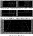
- FIG. 2 is a view showing the frequency distribution of the secondary voltage waveform, the average waveform between channels and the secondary voltage waveform measured in channels 2 to 5 according to the present invention
- 3 is a diagram showing a result of repeating averaging at every 5000 samples by removing the offset from the secondary waveform
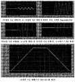
- FIG. 5 is a diagram showing a time waveform and a frequency distribution in which an integral method is used
- Fig. 6 is a view showing the calculation result of the secondary current without the fraction treatment
- FIG. 7 is a view showing the results of calculation of the primary current (100 A / s, 5 kS / s) using the additive average method of fractional treatment;
- FIG. 8 is a diagram showing the results of calculation of the primary current (20 A / s, 5 kS / s) using the additive average method of fractional treatment;
- Figure 9 is a schematic diagram showing a coil current measuring device for detecting the quench of the superconducting tokamak device according to the present invention.
- measuring means 200 processing means
- terminal 220 amplifier
- FIG. 1 is a schematic flowchart of a signal processing method for detecting a quench of a superconducting magnet operating current according to the present invention
- FIG. 2 is a secondary voltage waveform and an average channel-to-channel waveform measured in channels 2 to 5 according to the present invention
- 3 is a diagram illustrating a frequency distribution of a differential voltage waveform
- FIG. 3 is a diagram illustrating a result of removing an offset from a secondary waveform and repeating averaging every 5000 samples
- FIG. 4 is a diagram illustrating offset proper and offset improper results of a channel average.
- 5 shows a time waveform and a frequency distribution in which the integrating method is used.
- FIG. 6 is a diagram showing a result of calculating the secondary current without using the fraction treatment
- FIG. 7 is a diagram showing a result of calculating the primary current (100 A / s, 5 kS / s) using the additive average method of the fraction treatment
- 8 is a view showing the results of the calculation of the primary current (20 A / s, 5 kS / s) using the additive average method of the fraction treatment
- FIG. 9 is a coil current measuring apparatus for detecting the quench of the superconducting tokamak device according to the present invention. It is a schematic diagram showing.
- a quench detection device for detecting a quench of a superconducting coil provided in a superconducting tokamak device of a superconducting tokamak device, the quench detecting device provided in a normal bus bar 410 for supplying a current to the superconducting coil 400, Measuring means for detecting 100
- the processing means 200 for interpreting the measured value measured from the measuring means through a mathematical algorithm and outputting the final value, and receiving the measured value detected by the processing means to check whether the quench is generated.
- a central processing unit 300 for controlling the superconducting region of the tokamak device.
- Measuring means 100 is to be installed in the normal bus bar 410 for supplying a current to the superconducting coil to measure whether the superconducting coil and the bus line quench generation, to measure the current of the superconducting coil, the main of the present invention As a technical point, the measuring means is to use a Rogowski coil which can be installed in a normal bus bar.
- the normal busbar through which the current to be measured flows is magnetically coupled to the Rogowski coil to form a core-less transformer. Therefore, normal busbars are called primary conductors, and the current to be measured is the primary current. In addition, the induced voltage generated in the Rogowski coil is a secondary voltage.
- the winding axis is the permeability ⁇ (H / m)
- the cross section radius of the winding axis is r (m)
- the main radius is R (m)
- the number of turns of the conductor is N, the primary current.
- the electromotive force e s (V) generated in the Rogowski coil by I (A) is represented by Equation 1 below.
- K R is the mutual induction coefficient of the Rogowski coil.
- the primary current is expressed by Equation 2 below by integrating Equation 1 above.
- the primary current is a sinusoidal alternating current
- the primary current is simply calculated by measuring the secondary voltage as shown in Equation 1 using an AC voltmeter and converting the effective voltage into the effective current.
- the primary current is not a sinusoidal alternating current, it is necessary to perform time integration as in Equation 2 using an integrator.
- Rogowski coil's magnetic inductance L having a circular cross section is represented by Equation 3 below.
- the wound wire portion of the Rogowski coil is modeled as shown in Fig. 4, and the permittivity of the wound wire portion is ⁇ (F / m), the inner radius is ⁇ (m), the outer radius is b (m), and the length is (m) If the number of floors is n, the interlayer capacity Cs (F) of the Rogowski coil is expressed as in Equation 4 below.
- the Rogowski coil is not a pure voltage source, but has an RLC circuit inside itself. Especially in the high frequency range, gain (voltage at the end of coaxial cable) EMF generated in the coil Attention should be paid to the frequency characteristics such as), phase, resonant frequency, etc.
- the processing means 200 receives a value (secondary voltage) measured by the Rogowski coil, which is the measuring means, and outputs a value through software for mathematical modeling as mentioned above.
- the processing means is a PXI system is applied, the value of the signal processing using a scanner method.
- the measuring means it is preferable to receive and interpret the value measured by the measuring means using a personal computer which executes the numerical integration described above.
- a personal computer which executes the numerical integration described above.
- it is composed of a terminal 210, an amplifier 220, a digitizer 230 and a computer (240; PC) in order to electrically connect the measuring means 100 and the processing means, these are sequentially connected and measured Configure the means to receive the measured values measured.
- the terminal 210 is an electrical terminal block before the signal cable of the Rogowski coil flows into the processing means 200
- the amplification unit 220 is an analog signal of the measuring means 100 before digital conversion for performing numerical integration. By amplifying the signal to improve the signal to noise ratio (SNR).
- SNR signal to noise ratio
- the digitizer 230 converts the analog signal amplified by the amplifier 220 into digital, which is finally analyzed / processed by the computer.
- the waveform of the primary current is defined by the output voltage, the output current, their slew rates, and the latency.
- the Rogowski coil's voltage measurement and primary current energization are automatically coordinated by the LabVIEW program.
- the central processing means 300 is connected to the processing means 200 and is provided to monitor and control whether or not a quench occurs in real time.
- the central processing means is a computer network of the processing means and a network via Ethernet. It can be monitored and controlled at a long distance by connecting to a LAN and is also responsible for controlling the MPS (magnet power supply) that supplies current to the superconducting coil.
- MPS magnet power supply
- Whether the quench is detected is transmitted to the processing means in real time, and the central processing means (central server) confirms through monitoring by the administrator and controls the MPS to quickly process the quench generation.
- the central processing unit may be a general PC, and although not shown in the drawing, various functions such as a display unit, an interface for connecting to a network, and a setting unit for safety control according to quench generation are added.
- the signal processing method for detecting the quench of the superconducting magnet operating current will be described in order to determine whether the quench is generated by measuring the current flowing in the superconducting coil using the Rogowski coil as the measuring means.
- Figure 2 shows the frequency distribution of the secondary voltage waveforms measured in channels 2 to 5, the waveforms averaged between the channels, and the secondary voltage waveforms using FFT with the primary current power off. It was.
- the secondary voltage waveforms are both offset and noise.
- the second voltage outputs of the same Rogowski coil are connected to channels 2 through 5, and the polarities of the channels 2 and 5 are reversed.
- the average between the channels used herein considers the inverse of this polarity, and is represented by Equation 5 below.
- the voltage offsets are -1.76, -4.76, 23.2, -15.8 ⁇ v, respectively, and are scattered in each channel.
- any amplitude of noise is about ⁇ 37 ⁇ v.
- the frequency of the main noise is widely distributed in the high frequency region in addition to 60 Hz.
- the voltage offset is 10.5 ⁇ v
- the noise amplitude is less than ⁇ 6 ⁇ v.
- the peak heights seen in the frequency and distribution fell below 1/10, resulting in a flat distribution.
- the sampling rate of the original waveform is 5 kS / s
- the sampling rate of the repeated averaged result is 1 S / s.
- the amplitude of the ripple is from ⁇ 300 nV to ⁇ 400 nV, and the period is about 22 s.
- the amplitude of the ripple is ⁇ 100 nV, the period is unclear.
- the amplitude of the ripple is reduced from 1/3 to 1/4 by the average between the channels, and most of the ripples shown in FIG. 3 are also common to the amplification unit and the digitizer of each channel.
- the ripple period of each channel is about 22 s and is quite long, so the measurement or calculation of the voltage offset must take this long period into account. If you ignore this period and measure and calculate the voltage offset, you will get an error for the true voltage offset.
- the mutual induction coefficient K R of the Rogowski coil used here is 0.534483 ⁇ H, which is an optimum value calculated based on the primary current measurement result.
- the current waveform converted from the secondary voltage of the Rogowski coil is shown in FIG. Since primary current does not flow, primary current value is 0A. Each voltage offset is shown below the figure.
- the error of the current after 150 s is about 1 A, but with an inadequate offset (-1.905112 ⁇ V, average between 5 s).
- the error of the current is about 40 A.
- the ratio of the measurement time of the former and the latter offset is 8.8 times, but the difference in the offset is only -150 ⁇ V. However, this slight offset difference caused about 40A of current error.
- the current waveform at 150 s is about 3 A for current waveforms with an appropriate offset (10.49883 ⁇ V, 44 s average), and the current error is roughly 3 A for improper offsets (10.45214 ⁇ V, 5 s average). 15A.
- the difference in offset here is -46.7 nV.
- the tendency is the same as that of the channel 2, but the error of the current at the appropriate offset increases in the average between the channels. This is because measurements of channels with large drift, such as channels 4-5, are also included in the average value. In other words, the drift is very uneven between channels, and the error may be rather large due to the average between the channels.
- the rate of change of the primary current is 100 A / s, and when the charge and discharge from 0 A to 100 A are repeated 10 times, the numerically calculated secondary voltage waveform, the measured secondary voltage waveform, and the measured value are 100 samples.
- the secondary voltage waveform repeated every time and the measured value were repeatedly averaged every 100 samples after integration, and the secondary voltage waveform which was not loaded was shown in FIG.
- the sampling rate of the secondary voltage waveform is 5 kS / s, and the sampling rate of the waveform obtained by repeatedly averaging this for every 100 samples is 50 S / s.
- the measurement of the secondary voltage was started 60 seconds before the primary current was energized, and the voltage offset and noise in a state where no current was flowing were also measured.
- the measured value shown in FIG. 5 is subtracted from the average value of a store at time 0-44 s (2 * 22 s) as an offset.
- the crest value is considerably low, 53.5 ⁇ V.
- Frequency components are densely distributed from low frequency to high frequency, but the main component is in the low frequency region.
- noise of crest values 500-1300 ⁇ V covers the whole. From 60 to 140 s, the waveform has a pulsed amplitude, but this is not a true secondary voltage, but a noise from a current source. Comparing the calculated voltage with the measured voltage, it can be seen that it is quite low, about 1/24.
- the secondary voltage waveform averaged every 100 samples after the measurement shows that there is a pulse of about 60 ⁇ V crest value, and that the actual secondary voltage is also measured, and at the same time, it is entirely covered by noise of about 20 ⁇ V crest value. . Since the waveform has S / N of about 3, the S / N is improved by 72 times with only a simple repetition average. However, if you try to average more samples to reduce noise more, it is not practical because the number of samples after averaging is too small or you need to measure at high speed.
- the present invention it is very effective to convert the secondary voltage waveform into a waveform having a high S / N, and perform inverse conversion after performing noise processing.
- the time integration is used to convert the secondary voltage waveform into a waveform having a high S / N, and iteratively averages to perform time differentiation.
- This process is referred to as an integral method in the present invention, and the current waveform can be calculated by multiplying the mutual induction coefficient K R of the Rogowski coil without time differential, but the reason for not doing so is to add a secondary voltage waveform. This is because it is necessary to process.
- the voltage waveform obtained by time-integrating the measured secondary voltage waveform and repeating averaged every 100 samples and then time-differentiated is shown below in FIG. 3.
- the trapezium rule (primary) was used for the numerical integration method to avoid the reduction of the number of elements of the integration result.
- the voltage waveform using only the repetition average is compared with the voltage waveform using the integrating method.
- high frequency noise is reduced and S / N is about 35. Since the S / N of the measured value was about 1/24, the S / N is improved by about 840 times by the integrating method.
- the waveform close to the theoretically expected secondary voltage (pulse) was extracted by the integration method.
- Equation 6 represents a DC component, and the direction represents a fundamental wave and an nth order high frequency wave. Noise with a sufficiently short wavelength compared to the total length of the waveform is displayed at high frequency only and has no direct current component.
- Equation 9 the negative integral of sin wt is expressed by Equation 9 below, and the amplitude of the sin wave is reduced to 1 / w by the integral.
- the amplitude of the cos wave is also reduced to 1 / w by integration.
- the true secondary voltage is proportional to the time derivative of the primary current, it is converted into a waveform similar to the primary current (for example, square wave) by integration.
- S / N is greatly improved.
- the integration performed here does not convert the secondary voltage into the primary current in preparation for the noise processing.
- the final step of the signal processing method for the quench detection of the superconducting magnet operating current according to the present invention is the step of eliminating the micro voltage drift, and applying the fractional processing (quantization) to the minute and long period voltage drift remaining in the secondary voltage waveform. How to remove it.
- the drift is reduced by using the average between the channels of the equation (1).
- the secondary voltage waveform in which the minute voltage drift remains is converted into a primary current waveform. If the rate of change of the primary current is 100 A / s and the charge and discharge are repeated 10 times from 0 A to 100 A, the measured secondary voltage waveform is used.
- Equation 5 This is used in Equation 5 to average between the channels, subtract the offset, and remove the noise.
- the secondary voltage waveform thus obtained and the primary current waveform calculated by integrating the voltage waveform and multiplying the mutual induction coefficient K R of the Rogowski coil are shown in FIG. 6.
- the current measured using the shunt resistor appears in white, and the current measured using the Rogowski coil appears in red.
- the current value (red) measured using the Rogowski coil shows a transition between -0.6 A and 1.4 A during the period of no current (0 to 60 s). There is a drift, and there is a drift that transitions from -3.5 A to 0 A in the period (60 to 141 s) in which the pulse current flowed. The period of drift is either 22 to 24 s.
- the error of the measurement using the Rogowski coil to the measurement using the shunt (white) is -2.50A at the top and -2.62A at the end of the measurement (time 141s). to be.
- the drift of the primary current reaches 1 A after 150 s. Since the drift shown in the primary current waveform of FIG. 6 varies about 1.4 A between about 10 s, the peak value of the drift remaining in the secondary voltage is estimated to be about 71 nV maximum. And we can see that this residual drift is constantly changing at cycles 22-24s.
- a method for eliminating minute and long periods of voltage drift using a simple numerical operation is devised and the secondary voltage of the measurement time of about 140s is measured through the signal processing method according to the present invention for a secondary voltage waveform having a measurement time of about 140s.
- the error of the current was reduced to less than 1/5 compared with the result shown in FIG. 6 for the voltage waveform.
- drift zero was achieved in the direct current portion of the primary current waveform.
- the bottom of the char is cut off (finalized). For example, if the waveform is 10 ⁇ 1 ⁇ V and the drift is an irregular waveform of ⁇ 1 ⁇ V, a complete DC waveform can be obtained by cutting out the variation less than ⁇ 2 ⁇ V from the measured value.
- the measured value is V (V)
- the width of the measured value V called V (V)
- Equation 10 The fractional processing of V is defined as in Equation 10 below.
- the measured value V is fractionated in multiples of 2 ⁇ V, such as ⁇ ..., 8 ⁇ V, 10 ⁇ V, 12 ⁇ V, ... ⁇ .
- this makes it impossible to fully express numbers other than constant multiples such as 9 ⁇ V, 11 ⁇ V, and 13 ⁇ V, and a quantization error of size 2 ⁇ V becomes a problem.
- the secondary voltage waveform in which a small voltage drift remains is converted into a primary current waveform.
- the measurement is the same as in Fig. 6, and the rate of change of the primary current is 100 A / s.
- the measured secondary voltage waveform is averaged between channels using Equation 1, and the offset is removed and the noise is removed as described above.
- the measurement value is processed using the above Equation 7.
- the secondary voltage waveform obtained in this way and the voltage waveform are integrated and the Rogowski coil mutual induction coefficient
- the primary current waveform calculated by multiplying is shown in FIG. 7.
- the drift is zero in the period when no current flows (0 to 60 s), and the drift is -0.7A in the period where the pulse current flows (60 to 141 s). Trending between 0A.
- the error of the measured value using the Rogowski coil to the measured value using the shunt is -0.31A at the top and at the end of the measurement (time 141 s). Comparing the error of the primary current of FIG. 6 and FIG. 7, it can be seen that the error in FIG. 7 is 1/5 at 1/5 and the accuracy of calculating the primary current at the measured secondary voltage is improved.
- FIG. 8 the result shown in FIG. 8 is shown in FIG. 8 using the measured value of the change rate of 20A / s of electric current.
- the measured voltage waveform is covered with a high frequency noise of 1.3 mV with a crest value and S / N was only 0.8% (1.124), but the second voltage waveform with a crest value of 10 ⁇ V can be extracted cleanly. Can be.
- the error of the measurement using the Rogowski coil to the measurement using the shunt is -0.56A at the top and at the end of the measurement (time 140s). -0.23A. Comparing the result at 100 A / s shown in FIG. 7 with the result at 20 A / s in FIG. 8, the signal processing method of the present invention uses the signal processing method of the present invention. Quasi-DC current waveforms can be measured at practical levels.
- the present invention configured as described above has the advantage of measuring the current of the superconducting magnet through the Rogowski coil, which is a measuring means, and accurately determining whether the quench is generated by removing the error value as described above.
Landscapes
- Physics & Mathematics (AREA)
- General Physics & Mathematics (AREA)
- Measuring Instrument Details And Bridges, And Automatic Balancing Devices (AREA)
- Investigating Or Analyzing Materials By The Use Of Magnetic Means (AREA)
- Measuring Magnetic Variables (AREA)
- Measurement Of Current Or Voltage (AREA)
Abstract
본 발명은 초전도 자석 운전전류의 켄치 검출을 위한 신호처리방법에 관한 것으로, 초전도 코일의 켄치를 검출하기 위한 켄치 검출 장치에서 상기 초전도 코일에 전류를 공급하는 노말 버스바에 설치되어 초전도 코일의 전류를 측정하는 측정수단과, 상기 측정수단으로부터 측정된 측정값을 수학적 알고리즘을 통해 해석하여 측정값을 출력하는 처리수단 및 상기 처리수단에서 검출된 측정값을 전달받아 초전도 토카막 장치의 켄치 검출을 위한 신호처리방법에 있어서, 상기 측정수단에 의해 검출된 2차전압의 측정치에 포함된 전압 오프셋을 제거하는 단계, 적분법을 사용하여 상기 2차전압의 전압 노이즈를 제거하는 단계 및 2차전압의 전압파형에 대한 미소전압 드리프트를 제거하는 단계를 포함하여 구성되는 것을 특징으로 한다.
Description
본 발명은 초전도 자석 운전전류의 켄치 검출을 위한 신호처리방법에 관한 것으로, 초전도 토카막 장치의 켄치 검출을 위해 측정된 코일전류의 효과적인 처리방법을 위한 신호처리방법에 관한 것이다.
최근 세계적으로 에너지 개발에 관심이 부각되면서 향후 대체 에너지를 개발하기 위해 현재 국내에서 개발 중인 핵융합 실험장치인 초전도 토카막 장치(KSTAR : Korea Superconducting Tokamak Advanced Research)는 플라즈마 상태의 중수소를 강한 자기장으로 가두기 위한 토로이달(TF) 코일(TF 초전도 코일)과, 플라즈마를 발생시키고 그 위치와 모양을 제어하기 위한 포로이달(PF) 코일(PF 초전도 코일)들로 구성 및 중심 코일(CS 초전도 코일)로 구성된다.
현재까지 개발된 초전도 코일은 지구자장의 26만 배에 달하는 13테슬라의 자장을 얻을 수 있으며, 이러한 자장은 핵융합 반응에서 요구되는 플라즈마를 만들고 가두기 위해 필요한 것이다. 따라서 초전도 코일의 핵심 기술은 '관내연선도체'(CICC : Cable-in Conduit-Conductor)라고 알려진 각각의 전선을 감아 코일을 형성하여 초전도 코일을 제조함에 있다.
관내연선도체(CICC)는 35kA급의 대전류 운전을 위해서 360 또는 486가닥의 선재를 사각형의 금속관으로 둘러싸인 방식의 도체를 사용하여 자석을 제작하는 것으로, 초전도 코일의 운전 시 침입 또는 발생하는 열을 4.5K로 냉각하기 위해 약 5기압의 초임계 헬륨을 관내연선도체로 강제 순환시킨다.
도 1은 국내에서 제작되는 초전도 코일을 일예로 나타낸 도면이다. 도시된 바와 같이 초전도 코일(SC Magnet)은 고온의 플라즈마를 진공용기 벽에 닿지 않고 가두기 위한 것으로, 그 주요장치인 토카막장치를 보유하고 있다. 상기 토카막장치는 TF(Toroidal Field) 및 PF(Poloidal Field) 코일을 사용하여 플라즈마의 생성, 구속 및 제어를 담당한다.
TF(Toroidal Field) 및 PF(Poloidal Field)코일로 구성된 TF 초전도 코일(101)과 CS(Central Solenoid)코일로 구성된 CS 초전도 코일(103)과, PF(Poroidal Field)코일로 구성된 PF 초전도 코일(102) 및 각 초전도 코일을 연결하는 연결구조물로 이루어진다.
상기 TF 초전도 코일(101 ; 코일)은 약 35KA의 직류전류로 운전되며, 상기 CS 초전도 코일(103)과 PF 초전도 코일(102)은 펄스운전을 하여 상호 자장변화에 의한 기전력을 토러스(도우넛) 형상의 진공용기 내부에 발생시켜 플라즈마를 생성하고 플라즈마 전류 및 TF 자장과 함께 플라즈마를 구속시키는 역할을 수행한다.
이러한 초전도 코일은 운전 도중 AC 손실(자기장 변화에 따른 전압의 유도로 발생된 전류에 의해 발생되는 손실 ; 페러데이 법칙, 오옴의 법칙), 선재와 선재사이의 마찰 혹은 선재와 지지물 사이의 마찰 그리고 접촉저항에 의한 주울(Joule)열 발생 등의 연속적인 교란에너지가 존재한다. 이러한 현상으로 인해 초전도성을 잃고 상전도로 변화는 현상을 켄치(Quench)라 하며, 켄치는 선재의 온도상승을 만들게 되며 자석의 어떤 부분의 초전도성을 파괴시킨다.
만약 초전도성을 읽게 된 영역의 최소전파영역(Minimum propagation zone ; MPZ)보다 크게 되면 상전도 영역에서의 열 발생, 냉매로의 열전달, 그리고 비열과 열전도도에 의한 열 흡수 등의 복잡한 전기적, 열적현상에 의해 상전도 영역은 그 영역을 확장하게 된다.
이러한 과정 동안 켄치 초기 발생점은 가장 긴 시간동안 주울열 발생에 노출되어 있기 때문에 가장 높은 온도상승을 일으킨다. 국부적인 온도상승은 자석에 심각한 영향을 가져다 줄 수 있으며, 온도상승이 어느 정도 범위에 제한되어진다고 할지라도 상전도 영역에서 나타나는 수천 내지 수만 볼트의 과전압은 권선 사이 아크의 원인이 되기도 한다.
이러한 문제점을 해소하기 위한 토카막 장치의 초전도 코일은 켄치 검출 시스템이 필요한데, 초전도 코일의 형태 및 운전 조건 등을 고려하여 능동형 켄치 방식(Active Quench Protection)이 요구된다.
따라서 초전도 토카막 장치의 안정적인 운전을 위해 앞서 설명한 바와 같은 요소들에 의해 발생되는 켄치를 검출하는 장치가 요구되며, 또한, 24시간 가동되는 토카막 장치의 특성상 실시간으로 켄치 발생여부를 감시할 수 있는 시스템이 요구된다.
이에 따라 본 출원인은 대한민국 특허출원 제2007-00085134호 "초전도 토카막 장치의 켄치 검출장치 및 실시간 켄치 감시시스템"을 출원한 바와 있다. 이것은 전압탭 센서를 통해 발산된 에너지를 검출하는 것으로, 켄치 검출 방식은 운전 도중에 초전도 코일에 설치된 전압탭 센서의 신호를 이용하여 켄치를 판단하며, 켄치가 검출되면 저장된 에너지가 자석이 아니 외부의 장치에서 빠르게 소비될 수 있도록 적절한 조치를 취해줄 수 있는 기술개발을 달성하였다.
하지만, 종래 켄치 검출장치는 코일에 부착된 전압탭 센서를 이용하기 때문에 센서 신호와 코일 전류와의 관계를 알 수 없기 때문에 코일 전류와 전압 신호의 상호 분석이 켄치 검출 장치의 안정성을 향상하기 위해서는 반드시 필수적이다.
초전도 코일의 전류를 측정하는 장치로 가장 단순한 형태의 션트 저항은 직접 노말 버스바에 결합하는 형태이므로 설치가 어렵고, Joule 발열 문제로 장치의 대형화를 초래하며, DC current transformer(DCCT)도 직접 노말 버스바에 결합하는 형태로 높은 전류를 측정하기 위해서는 매우 높은 비용이 요구되는 문제점이 있다.
이러한 문제점을 해결하기 위하여 본 출원인은 노말 버스바에 설치되어 코일전류를 측정함으로써 초전도 자석의 켄치 발생여부를 검출하기 위한 초전도 토카막 장치의 켄치 검출을 개발한 바 있으나, 초전도 코일에서 측정된 전류를 이용하여 보다 정확하게 켄치 검출여부를 확인하기 위한 신호처리개발이 필요한 실정이다.
상기와 같은 문제점을 해결하기 위한 본 발명은 초전도 코일의 켄치를 검출하기 위해 코일전류를 측정하고, 측정된 전류를 효과적으로 처리하여 신뢰성 높은 켄치 발생여부 판단을 달성하기 위한 것에 그 목적이 있다.
상기와 같은 목적을 달성하기 위한 본 발명은 초전도 코일의 켄치를 검출하기 위한 켄치 검출 장치에서 상기 초전도 코일에 전류를 공급하는 노말 버스바에 설치되어 초전도 코일의 전류를 측정하는 측정수단과, 상기 측정수단으로부터 측정된 측정값을 수학적 알고리즘을 통해 해석하여 측정값을 출력하는 처리수단 및 상기 측정수단으로부터 측정된 측정값을 수학적 알고리즘을 통해 해석하여 측정값을 출력하는 처리수단 및 상기 처리수단에서 검출된 측정값을 전달받아 초전도 토카막 장치의 켄치 검출을 위한 신호처리방법에 있어서, 상기 측정수단에 의해 검출된 2차전압의 측정치에 포함된 전압 오프셋을 제거하는 단계, 적분법을 사용하여 상기 2차전압의 전압 노이즈를 제거하는 단계 및 2차전압의 전압파형에 대한 미소전압 드리프트를 제거하는 단계를 포함하여 구성되는 것을 특징으로 한다.
또한, 상기 전압 오프셋 제거단계에서는, 채널 2 내지 채널 5를 통해 상기 측정수단으로부터 측정되는 2차전압 출력을 접속시키고, 상기 채널간 평균은,  에 의해서 산출되는 것을 특징으로 한다.
또한, 상기 전압 오프셋 제거단계에서는, 장주기의 리플 주기를 나누고, 이 주기의 정수배의 시간에 걸쳐 2차전압 파형을 측정하여 상가 평균하는 것에 의해 전압 오프셋을 산출하는 것을 특징으로 한다.
또한, 상기 미소 전압 드리프트 단계는, 수학식

또한, 상기 측정수단은, Rogowski코일을 사용하는 것을 특징으로 한다.
또한, 상기 측정수단은, 수학식  를 통해 전압을 시간 적분하여 측정값을 산출하는 것을 특징으로 한다.
또한, 상기 측정수단은, 상기 노말 버스바에 설치되어 이와 자기적으로 결합함에 따라 core-less 트랜스를 형성하는 것에 의해 전류를 검출하는 것을 특징으로 한다.
또한, 상기 처리수단은, 상기 측정수단과 연결되는 터미널, 상기 터미널에서 제공되는 전압을 전달받는 증폭부, 상기 증폭부에서 제공되는 전압값을 수치화하는 디지타이저 및 상기 디지타이저를 통해 제공되는 전압값을 수학적 모델링을 통해 해석하여 켄치 발생여부를 검출하는 컴퓨터로 구성되는 것을 특징으로 한다.
또한, 상기 전압 오프셋 제거단계에서는, 샘플마다 반복 평균한 결과에서 오프셋을 제거하는 것을 특징으로 한다.
상기와 같이 구성되고 작용되는 본 발명은 Rogowski코일을 통해 초전도 자석의 전류를 측정하고 오차값을 제거하여 켄치 발생여부를 정확하게 판단할 수 있는 이점이 있다.
도 1은 본 발명에 따른 초전도 자석 운전전류의 켄치 검출을 위한 신호처리방법의 개락적인 순서도,
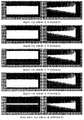
도 2는 본 발명에 따른 채널 2 내지 채널 5에서 측정된 2차전압 파형과 채널간 평균 파형 및 2차전압 파형의 주파수 분포를 나타낸 도면,
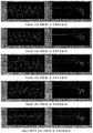
도 3은 2차 파형에서 오프셋을 제거하고 5000샘플마다에 반복 평균한 결과를 나타낸 도면,
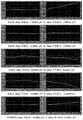
도 4는 채널 평균의 오프셋 적절 및 오프셋 부적절 결과를 나타낸 도면,
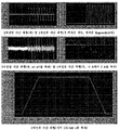
도 5는 가 적분법이 사용된 시간 파형 및 주파수 분포를 나타낸 도면,
도 6은 끝수 처리를 사용하지 않은 2차전류의 산출 결과를 나타낸 도면,
도 7은 끝수 처리의 상가평균법을 사용한 1차전류의 산출(100 A/s, 5 kS/s) 결과를 나타낸 도면,
도 8은 끝수 처리의 상가평균법을 사용한 1차전류의 산출(20 A/s, 5 kS/s) 결과를 나타낸 도면,
도 9는 본 발명에 따른 초전도 토카막 장치의 켄치 검출을 위한 코일전류 측정장치를 나타낸 개략도.
<도면의 주요부분에 대한 부호의 설명>
100 : 측정수단 200 : 처리수단
210 : 터미널 220 : 증폭부
230 : 디지타이저 240 : 컴퓨터
300 : 중앙처리수단 400 : 초전도 코일
410 : 노말 버스바
이하, 첨부된 도면을 참조하여 본 발명에 따른 초전도 자석 운전전류의 켄치 검출을 위한 신호처리방법의 바람직한 실시예를 상세히 설명하면 다음과 같다.
도 1은 본 발명에 따른 초전도 자석 운전전류의 켄치 검출을 위한 신호처리방법의 개락적인 순서도, 도 2는 본 발명에 따른 채널 2 내지 채널 5에서 측정된 2차전압 파형과 채널간 평균 파형 및 2차전압 파형의 주파수 분포를 나타낸 도면, 도 3은 2차 파형에서 오프셋을 제거하고 5000샘플마다에 반복 평균한 결과를 나타낸 도면, 도 4는 채널 평균의 오프셋 적절 및 오프셋 부적절 결과를 나타낸 도면, 도 5는 가 적분법이 사용된 시간 파형 및 주파수 분포를 나타낸 도면이다.
도 6은 끝수 처리를 사용하지 않은 2차전류의 산출 결과를 나타낸 도면, 도 7은 끝수 처리의 상가평균법을 사용한 1차전류의 산출(100 A/s, 5 kS/s) 결과를 나타낸 도면, 도 8은 끝수 처리의 상가평균법을 사용한 1차전류의 산출(20 A/s, 5 kS/s) 결과를 나타낸 도면, 도 9는 본 발명에 따른 초전도 토카막 장치의 켄치 검출을 위한 코일전류 측정장치를 나타낸 개략도이다.
우선, 본 발명에 따른 초전도 자석 운전전류의 켄치 검출을 위한 장치에 대하여 개략적으로 언급한다.
초전도 토카막 장치의 초전도 토카막 장치에 구비되는 초전도 코일의 켄치를 검출하기 위한 켄치 검출 장치에 있어서, 상기 초전도 코일(400)에 전류를 공급하는 노말 버스바(410)에 설치되어 초전도 코일에 흐르는 전류를 검출하기 위한 측정수단(100) 상기 측정수단으로부터 측정된 측정값을 수학적 알고리즘을 통해 해석하여 최종값을 출력하는 처리수단(200) 및 상기 처리수단에서 검출된 측정값을 전달받아 켄치발생 여부를 확인하여 토카막 장치의 초전도 영역을 제어하는 중앙처리수단(300)을 포함한다.
측정수단(100)은 초전도 코일 및 버스라인의 켄치 발생여부를 측정하기 위해 초전도 코일로 전류를 공급하기 위한 노말 버스바(410)에 설치되어 초전도 코일의 전류를 측정하기 위한 것으로, 본 발명의 주요 기술적 요지로 상기 측정수단으로는 노말 버스바에 설치할 수 있는 Rogowski(로고스키)코일을 사용하는 것으로 한다.
측정대상의 전류가 흐르는 노말 버스바는 상기 Rogowski 코일과 자기적으로 결합하여 core-less트랜스를 형성한다. 따라서 노말 버스바는 1차 도체라고 불리고, 측정대상의 전류는 1차전류로 한다. 또한, 상기 Rogowski코일에서 발생하는 유도전압은 2차전압으로 한다.
원형단면을 가진 Rogowski코일에 대해, 감은 축은 투자율을 μ(H/m), 감은 축의 단면반경을 r(m), 주반경을 R(m), 도선의 감은 수를 N이라고 한다면, 1차전류 I(A)에 의해 Rogowski코일에 발생한 기전력 es(V)는 아래 수학식 1로 표시된다.
수학식 1 
여기에서 KR 상기 Rogowski 코일의 상호 유도계수이다. 1차전류는 상기 수학식 1을 시간 적분하여 아래 수학식 2로 표시된다.
수학식 2 
만약 1차전류가 정현파 교류전류라면, 상기 수학식 1과 같은 2차전압을 교류 전압계를 사용하여 측정하고, 실효전압을 실효전류로 환산하는 것에 의해, 1차전류는 간단히 산출된다. 이것에 대해 1차전류가 정현파 교류전류가 아니라면, 적분기를 사용하여 상기 수학식 2와 같은 시간 적분을 할 필요가 있다.
상기 Rogowski코일의 전기특성의 등가회로는 도 3과 같이 표시된다. 여기서 감은 선의 저항은 rc (Ω), 자기 인덕턴스를 L(H), 감은 선의 분포용량과 동축케이블의 정전용량을 합성한 것을 C(F), 동축케이블 끝머리에서의 ringing을 방지하기 위한 damping 저항을 Rd (Ω)로 표시한다.
원형단면을 가진 Rogowski코일의 자기 인덕턴스 L은 아래 수학식 3으로 표시된다.
수학식 3 
상기 Rogowski코일의 감은 선 부분을 도 4에 나타낸 바와 같이 모델화하여 감은 선부분의 유전율을 ε(F/m), 내반경을 α(m), 외반경을 b(m), 길이를  (m), 층수를 n으로 한다면, Rogowski코일의 층간용량 Cs(F)는 아래 수학식 4와 같이 표시된다.
수학식 4 
위와 같이, Rogowski코일은 순수한 전압원이 아니라, 그 자체의 내부에 RLC회로를 갖는다. 특히 고주파 영역에서는 gain(동축케이블 끝머리에서의 전압  /코일에 발생하는 기전력
  ), 위상, 공진주파수 등의 주파수 특성에 주의가 필요하다.
처리수단(200)은 상기 측정수단인 Rogowski코일에서 측정된 값(2차전압)을 입력받아 앞서 언급한 바와 같이 수학적 모델링을 위한 소프트웨어를 통해 값을 출력한다. 더불어 상기 처리수단은 PXI 시스템을 적용한 것으로, 스캐너 방식을 이용하여 값을 해당 신호를 처리한다.
또한, 바람직하게는 앞서 설명한 수치적분을 실행하는 퍼스널 컴퓨터를 사용하여 상기 측정수단에서 측정된 값을 제공받아 해석한다. 이때 상기 측정수단(100)과 처리수단을 연결하기 전기적으로 상호 연결하기 위하여 터미널(210), 증폭부(220), 디지타이저(230) 및 컴퓨터(240 ; PC)로 구성되고 이들이 순차적으로 연결되어 측정수단에서 측정된 측정값을 전달받도록 구성한다. 상기 터미널(210)은 Rogowski코일의 신호케이블이 처리수단(200)에 유입되기 전의 전기적인 단자대이며, 상기 증폭부(220)는 수치적분을 수행하기 위한 디지털 변환 전에 측정수단(100)의 아날로그 신호를 증폭하여 SNR(Signal to Noise Ratio)를 향상시키기 위한 것이다.
또한, 상기 디지타이저(230)는 증폭부(220)에 의해 증폭된 아날로그 신호를 디지털로 변화시키고, 이 디지털 신호는 상기 컴퓨터에 의해 최종적으로 분석/처리하게 된다.
1차전류의 파형은 출력전압, 출력전류, 그것들의 변화율(slew rates), 대기시간에 의해 정의된다. Rogowski코일의 전압 측정과 1차전류 통전은 LabVIEW 프로그램에 의해 자동적으로 연동하게 된다.
중앙처리수단(300)은 상기 처리수단(200)과 연결되어 켄치 발생 여부를 실시간으로 모니터링 및 제어하기 위하여 구비되는 것으로, 상기 중앙처리수단은 상기 처리수단의 컴퓨터(240)와 이더넷을 통한 네트워크망(LAN)으로 연결되어 원거리에서 모니터링과 제어를 할 수 있으며, 초전도 코일로 전류를 공급하는 MPS(magnet Power Supply)의 제어도 담당한다.
상기 처리수단에 검출된 켄치 발생여부를 실시간으로 전송하며, 중앙처리수단(중앙서버)에서는 관리자에 의한 모니터링을 통해 확인하고 MPS를 제어하여 켄치 발생 시 신속히 처리한다.
상기 중앙처리수단은 일반적인 PC가 되며, 도면에 나타내진 않았지만, 디스플레이부, 네트워크와 연결되기 위한 인터페이스, 켄치 발생에 따른 안전 제어를 위한 설정부 등 다양한 기능을 부가되어 있다.
앞서 설명한 바와 같이 Rogowski코일을 측정수단으로 이용하여 초전도 코일에 흐르는 전류를 측정하여 켄치 발생여부를 확인하기 위하여 본 발명에 따른 초전도 자석 운전전류의 켄치 검출을 위한 신호처리방법을 설명한다.
우선, 측정수단이 가진 오프셋 및 노이즈 레벨에 대해 서술한다. 1차전류의 전원의 출력이 off의 상태에서 채널 2부터 채널 5에서 측정된 2차전압 파형 및 그것들은 채널간에서 평균한 파형, 그리고 FFT를 사용한 2차전압 파형의 주파수 분포를 도 2에 나타내었다.
2차전압 파형은 모두 오프셋 및 노이즈이다. 채널 2부터 채널 5에는 동일한 Rogowski코일의 2차전압 출력이 접속되어 있고, 채널 2 및 채널 5의 ±극성은 반전되어 있다. 여기에서 사용한 채널간의 평균은 이 극성의 반적을 고려하였고, 아래 수학식 5와 같이 나타내었다.
수학식 5 
수학식 5의 계산결과에서는, Rogowski코일의 2차전압은 변화하지 않으나, 각 채널의 증폭부 및 디지타이저가 공통으로 갖는 오프셋과 노이즈는 캔슬된다.
도 2에 도시된 바와 같이 채널 2부터 채널 5의 2차전압 파형을 비교해보면, 전압 오프셋은 각각 -1.76, -4.76, 23.2, -15.8 μv이고, 채널마다에 흩어져있다. 이것에 대해 노이즈의 진폭은 어느 것이나 모두 약 ±37μv이다. 또한 주된 노이즈의 주파수는 60 Hz 이외에도, 그것보다 고주파수 영역에 넓게 분포되어 있다. 한편, 상기 수학식 5와 같이 채널간에서 평균한 파형을 보면, 전압 오프셋은 10.5 μv이고, 노이즈의 진폭은 ±6 μv미만이다. 또한 주파수, 분포에서 볼 수 있는 피크의 파고가 1/10이하로 저하하여, 분포가 평탄하게 되었다.
수학식 5에 표시된 채널간의 평균에 의해 노이즈의 진폭이 약1/6으로 저하한 것에서 도 3에 나타낸 노이즈의 대부분은 각 채널의 평균에 의해 전압 오프셋은 캔슬되어 있지 않다는 것에서 전압 오프셋은 채널마다 흩어져 있다는 것을 알 수 있다.
상기 측정수단이 갖는 장주기 노이즈(이른바 리플)의 주기에 대해 서술한다. 도 3에 도시된 바와 같이 2차전압 파형에서 오프셋을 제거하고, 5000샘플마다에 반복 평균한 결과를 도 4에 나타내었다.
원래의 파형의 샘플링 속도는 5 kS/s이기에, 반복 평균한 결과의 샘플링 속도는 1 S/s이다.
도 4에 표시된 채널 2부터 채널 5의 2차전압 파형을 비교해 보면, 리플의 진폭은 ±300 nV에서 ±400 nV까지이고, 주기는 약 22 s이다. 한편, 수학식 1과 같이 채널간에 평균한 파형을 보면, 리플의 진폭은 ±100 nV이고, 주기는 불명료하다.
채널간의 평균에 의해 리플의 진폭이 1/3에서 1/4 저하 한 것으로, 도 3에 표시된 리플의 대부분도 역시 각 채널의 증폭부 및 디지타이저에 공통의 리플이라는 것을 알 수 있다. 각 채널의 리플의 주기는 약 22s이고 상당히 길기에 전압 오프셋의 측정이나 산출은 이 장주기를 고려하지 않으면 안 된다. 만일 이 주기를 무시하고 전압 오프셋을 측정하여 산출했다면 진정한 전압 오프셋에 대해 오차를 만들어낸다.
전압 오프셋의 제거가 적절한 경우와 부적절한 경우에 대해 Rogowski코일의 2차전압에서 환산된 전류 파형을 비교해 본다. 전류 파형을 산출하면 도 2에서 표시된 2차전압 파형에서 오프셋을 빼고 시간 적분하여 Rogowski코일의 상호 유도계수 KR을 곱하면 된다. 여기에서 적절한 오프셋으로서 2차전압 파형을 시각 0 ~ 44 s(2*22s)에 걸쳐 상가 평균한 값을 사용하고, 부적절한 오프셋으로서 2차전압 파형을 시각 0 ~ 5s(0.227*22s)에 걸쳐 상가 평균한 값을 사용한다.
또 여기에서 사용하는 Rogowski코일의 상호 유도계수 KR 은 0.534483 μH이고, 1차전류의 측정결과에 근거하여 산출된 최적치이다. Rogowski코일의 2차전압으로부터 환산된 전류 파형을 도 4에 나타낸다. 1차전류는 흐르고 있지 않기에 1차전류치는 0A이다. 도면 아래 각각 전압 오프셋을 표시했다.
도 4의 채널 2를 보면, 적절한 오프셋(-11.755181 μV, 44 s간 평균)의 전류 파형에서는 150 s후의 전류의 오차가 1 A정도이지만, 부적한 오프셋(-1.905112 μV, 5 s간 평균)에서는 전류의 오차가 약 40 A나 된다. 전자와 후자의 오프셋의 측정시간의 비는 8.8배나 되지만, 오프셋의 차는 -150 μV밖에 없다. 그러나 이 극소한 오프셋의 차에 의해 전류의 오차가 약 40A나 발생됐다.
채널간의 평균을 보면, 적절한 오프셋(10.49883 μV, 44 s간 평균)의 전류 파형에서는 150 s후의 전류의 오차가 3 A정도이고, 부적절한 오프셋(10.45214 μV, 5 s간 평균)에서는 전류의 오차가 약 15A이다. 여기서 오프셋의 차는 -46.7 nV이다. 경향으로서는 채널 2의 결과와 같으나, 채널간의 평균에서는 적절한 오프셋에서의 전류의 오차가 늘어나 있다. 이것은 채널 4 ~ 5와 같은 드리프트가 큰 채널의 측정치도 평균치에 포함되어 있기 때문이다. 즉, 드리프트는 채널간의 불균일성이 심하여, 채널간의 평균에 의해 오히려 오차가 커질 경우도 있다.
상술한 바에서 알 수 있듯이, Rogowski코일의 2차전압에서 1차전류를 정확하게 환산하기 위해서는 측정된 2차전압 파형에서 극히 정확한 오프셋을 뺄 필요가 없다. 이를 위해서는 장주기의 리플의 주기를 할 수 있는 한 정확하게 나누어, 이 주기의 정수배의 시간에 걸쳐 2차전압 파형을 측정하여 상가 평균하는 것에 의해 전압 오프셋을 산출할 필요가 있다.
다음으로 가 적분법을 행하여 측정된 2차전압 파형의 노이즈를 효과적으로 제거단계(S300)에 대해 서술한다. 1차전류의 변화 속도를 100A/s라고 하고, 0 A에서 100A까지의 충전 및 방전을 10회 반복했을 경우에 대해, 수치 계산된 2차전압 파형, 측정된 2차전압 파형, 측정치를 100샘플마다 반복한 2차전압 파형, 측정치를 적분해 100샘플마다에 반복평균하고 나서 미부한 2차전압 파형을 도 5에 나타내었다. 2차전압 파형의 샘플링 속도는 5 kS/s이고, 이것을 100샘플마다에 반복 평균한 파형의 샘플링 속도는 50 S/s이다.
또한, 1차전류를 통전하는 60s전에는 2차전압의 측정을 개시하여 전류가 흐르고 있지 않는 상태에서의 전압 오프셋 및 노이즈도 측정했다. 도 5에 표시된 측정치는 오프셋으로서 시각 0 ~ 44 s (2*22 s)의 상가 평균치를 차감되어져 있다.
먼저 도 5의 수치 계산된 2차전압 파형을 보면, 파고치가 53.5 μV로 상당히 낮다. 주파수성분은 저주파에서 고주파까지 조밀하게 분포하고 있으나, 주요한 성분은 저주파 영역에 있다는 것이다. 측정된 2차전압 파형을 보면, 파고치 500-1300 μV의 노이즈가 전체를 덮고 있다. 60 ~ 140 s에서 파형에 펄스형의 진폭이 있으나, 이것은 진정한 2차전압이 아니라, 전류원이 발생한 노이즈이다. 수치 계산된 전압과 측정된 전압을 비교해 보면, 1/24정도로 상당히 낮다는 것을 알 수 있다.
측정 후 100샘플마다 평균된 2차전압 파형을 보면, 파고치 약 60 μV의 펄스가 있고, 실제 2차전압도 측정되어 있다는 것을 알 수 있으며, 동시에 파고치 약 20 μV의 노이즈에 의해 전체가 덮여 있다. 이 파형은 S/N은 3정도이기에, 단순한 반복평균만으로는 S/N이 72배 개선되게 된다. 단, 노이즈를 좀 더 줄이기 위해 보다 많은 샘플을 평균하려고 한다면 평균 후의 샘플 수가 너무 적어지거나 고속으로 측정할 필요가 생겨 실용적이지 못하다.
디지털 low-pass 필터를 사용한 수단도 있으나, 수치 계산의 결과와 같이 펄스 파형의주파수 성분은 저주파에서 고주파까지 조밀하게 분포되어 있기에, 강도가 강한 필터를 걸면 2차전압의 파형이 일그러져 버릴 수 있다. 노이즈 처리를 곤란하게 하는 원인은 S/N의 낮음이다. Rogowski코일은 본질적으로 S/N을 높이는 것이 어려운 수단이고, 감도(1차 2차간의 상호 인덕턴스)를 높이기 위해 단순하게 센서를 거대화하면, 노이즈도 늘어나기 때문에 S/N은 개선되지 않고, 더욱이 코스트가 늘어나 제작이 어려워지거나 전기적 특성이 나빠지게 된다.
이러한 문제점 때문에 본 발명에서는 2차전압 파형을 S/N이 높은 파형으로 변환하고, 노이즈 처리를 하고 나서 역변환하면 매우 효과적이다.
따라서, 본 발명에서는 시간적분을 이용하여 2차전압 파형을 S/N이 높은 파형으로 변환하고, 반복 평균을 행하여 시간미분을 실시하였다. 이러한 과정을 본 발명에서는 가 적분법이라 칭하며, 여기에서 시간미분하지 않고 Rogowski코일의 상호 유도계수 KR 을 곱하면 전류 파형을 산출할 수 있으나, 그와 같이 하지 않는 이유는 2차전압 파형을 추가로 가공할 필요가 있기 때문이다. 측정된 2차전압 파형을 시간 적분하여 100샘플마다에 반복평균하고 나서 시간 미분한 전압 파형은 도 3 아래 표시되었다.
적분 결과의 요소수의 감소를 피하게 위해 수치적분의 방법에는 trapezium rule(1차)를 사용했다.
반복 평균만을 사용한 전압 파형과 가 적분법을 사용한 전압 파형을 비교해 보며나 가 적분법을 사용한 전압 파형에서는 고주파 노이즈가 격감하고, S/N은 약 35이다. 측정치의 S/N은 약 1/24였기에 가적분법에 의해 S/N이 약 840배나 개선되게 된다. 또 수치 계산된 전압 파형과 비교해 보면 이론적으로 예상된 2차전압(펄스)에 가까운 파형이 가 적분법에 의해 추출되었다는 것을 알 수 있다.
즉 가 적분법을 사용하여 고주파 노이즈의 제거와 펄스파형의 추출을 양립시키는 것이 가능하다는 것을 알 수 있다.
가 적분법의 원리는 다음과 같다. 기본 각 주파수를  (rad/s)라고 한다면 측정된 2차전압은 Fourier 급수전개를 사용하여 아래 수학식 6 내지 8과 같이 근사된다.
수학식 6 
수학식 7 
수학식 8 
상기 수학식 6의 초항은 직류성분을, 차향은 기본파 및 n차 고주파를 나타낸다. 파형의 전체길이와 비교하여 충분히 짧은 파장을 가진 노이즈는 고주파만으로 표시되고, 직류성분을 갖지 않는다. 여기에서, sin wt의 부정적분은 아래 수학식 9에서 나타내고, sin파의 진폭은 적분에 의해 1/w로 감소한다는 것을 알 수 있다.
수학식 9 
마찬가지로, cos파의 진폭도 적분에 의해 1/w로 감소한다. 즉 고주파만으로 나타나지는 노이즈의 진폭은 적분에 의해 격감한다는 것을 알 수 있다. 이것에 대해 진정한 2차전압은 1차전류의 시간미분에 비례하기에 적분에 의해 1차전류에 상사한 파형(예를 들면 square wave)으로 변환된다. 결과로서 측정된 2차전압을 적분하는 것에 의해, S/N이 대폭으로 개선된다. 단, 여기에서 행해진 적분은 노이즈 처리의 준비로 2차전압을 1차전류로 환산한 것은 아니다.
본 발명에 따른 초전도 자석 운전전류의 켄치 검출을 위한 신호처리방법의 마지막 단계는 미소 전압 드리프트의 제거 단계로써, 끝수 처리(양자화)를 응용하여 2차전압 파형에 잔류하는 미소하고 주기가 긴 전압 드리프트를 제거하는 방법을 설명한다.
이것은 2차전압 파형의 파고치에 대해 전압 드리프트가 충분히 작은 경우에만 유효하다. 만일 전압 드리프트가 큰 경우에는 사전에 어떠한 방법을 사용하여, 드리프트를 충분히 작게 해 둘 필요가 없다. 본 발명에서는 수학식 1의 채널간의 평균을 이용하여 드리프트를 삭감했다.
좀 더 확실하게 드리프트를 삭감하기 위해서는 Rogowski코일의 2차전압의 극성을 전기회로로 주기적으로 반전시키는 방법을 사용하여 증폭부 및 디지타이저에서 발생하는 전압 드리프트를 상쇄할 필요가 있다.
미소 전압 드리프트가 잔류하고 있는 2차전압 파형을 1차전류 파형으로 환산하여 본다. 1차전류의 변화속도를 100 A/s로 하고, 0 A에서 100 A까지의 충전 및 방전을 10회 반복한 경우네 측정된 2차전압 파형을 사용한다.
이것을 수학식 5에 사용하여 채널간에서 평균하고, 오프셋을 빼고, 노이즈를 제거한다. 이렇게 얻어진 2차전압 파형 및 이 전압 파형을 적분하고 Rogowski코일의 상호 유도계수 KR 을 곱해 산출된 1차전류 파형을 도 6에 나타낸다. 여기서 전류 파형에서는 션트저항을 사용하여 측정된 전류치가 백색으로 나타나고, Rogowski코일을 사용하여 측정된 전류치가 적색으로 나타난다.
2차전압 파형을 보면, 전압 드리프트는 거의 없는 듯이 보이나, Rogowski코일을 사용하여 측정된 전류치(적색)를 보면 전류가 흐르지 않는 기간(0 ~ 60 s)에는 -0.6 A에서 1.4 A사이에서 추이하는 드리프트가 있고, 펄스 전류가 흘렀던 기간(60 ~ 141s)에는 -3.5A에서 0A사이에 추이하는 드리프트가 있다. 드리프트의 주기는 어느 쪽이나 22 ~ 24s이다. 또한 1차전류 파형의 시각 135 ~ 141s를 확대한 도면을 보면 션트를 사용한 측정치(백색)에 대한 Rogowski코일을 사용한 측정치의 오차는 정상부에서 -2.50A, 측정 종료 시(시간 141s)에서 -2.62A이다.
서술한 측정결과에 근거하면 2차전압에 3.4 nV의 오프셋이 있으면 1차전류의 드리프트는 150s후에 1A에 달한다. 도 6의 1차전류 파형에 보여지는 드리프트는 약 10s간에 약 1.4A 변화하고 있기에 2차전압에 잔류하는 드리프트의 파고치는 최대 71nV정도라고 추정된다. 그리고 이 잔류 드리프트는 주기 22 ~ 24s에서 끊임없이 계속 변화하고 있다는 것을 알 수 있다.
Rogowski코일을 사용한 전류의 측정 수법에서, 일반적으로는 이와 같은 미소하고 주기가 긴 전압 드리프트를 완전하게 제거하는 것은 극히 곤란하다. 특히, 측정시간이 100s를 넘는 장시간의 준직류전류 파형을 실용적인 레벨에서 측정할 수 없다.
본 발명에서는 단순한 수치연산을 이용하여 미소하고 주기가 긴 전압 드리프트를 제거하는 방법을 고안하고 측정시간 약 140s의 2차전압 파형에 대해 본 발명에 따른 신호처리방법을 통해 측정시간 약 140s의 2차전압 파형에 대해 도 6에 도시된 결과와 비교하여 전류의 오차를 1/5이하로 감소시켰다. 특히, 1차전류 파형의 직류부분에서 드리프트 제로를 달성했다.
실험결과를 통해 아래에서 좀 더 상세히 설명한다.
평균처리나 필터 등을 사용해도 완전하게는 제거할 수없는 미소하고 주기가 긴 또는 불규칙한 전압 드리프트를 측정치에서 수치적으로 제거하기 위해서는, 숯의 아래 자리를 잘라 버리면(끝수 처리함)된다. 예를 들면, 파형이 10 ±1μV이고 이 중에 드리프트가 ±1 μV의 불규칙한 파형이라고 한다면, ±2μV 미만의 변하를 측정치에서 잘라내는 것에 의해 완전한 직류파형을 얻을 수 있다. 여기에서 측정치를 V(V), 끝수 처리의 폭을  V(V)라고 하고 측정치 V의 폭
  V의 끝수 처리를 아래 수학식 10과 같이 정의한다.
수학식 10 

그래서 측정치의 복수 폭의 끝수 처리를 수행하고, 그것들의 상가평균치를 끝수 처리의 결과라고 한다. 1이상의 임의의 수를  라고 하고, 측정치 V의 복수 폭
  의 끝수 처리의 상가평균을 아래 수학식 11과 같이 정의한다.
수학식 11 
다음으로 실제 수학식 11을 사용하여 미소한 전압 드리프트가 잔류하고 있는 2차전압 파형을 1차전류 파형으로 환산해 본다. 측정치는 도 6고 같은 것이고, 1차전류의 변화속도는 100A/s이다. 측정된 2차전압 파형을 수학식 1을 사용하여 채널간에서 평균하고, 앞서 설명한 바와 같이 오프셋을 제거하고 노이즈를 제거한다. 그리고 마지막으로 상기 수학식 7을 이용하여 측정치를 끝수 처리한다. 여기에서는  =2.5μV, {
 }={1.0, 1.1, 1.2, ...,1.9}로 했다. 이렇게 해서 얻어진 2차전압 파형 및 이 전압 파형을 적분하고 Rogowski코일의 상호 유도계수
  를 곱하여 산출된 1차전류 파형을 도 7에 나타내었다.
도 6과 도 7은 2차전압 파형을 비교해 보면, 도 7의 전압 파형에서는 고주파의 노이즈 및 미소한 드리프트이 대부분이 제거되어 있다. 또 ±4 μV의 확대 그림을 보면, 크기가 4μV만으로 측정치를 끝수 처리한 경우에는 수치가 폭 4μV의 정수배가 되기 때문에 이와 같은 작은 데이터점과 정수배 이외의 수는 존재할 수 없다. 한편, 여기에서 사용한 수법에는 복수의 폭에 대한 끝수 처리의 결과(제로를 포함)를 평균하고 있기에, 확대 그림과 같은 4μV미만의 데이터 점 및 폭의 정수배 이외의 값이 존재 가능하다. 이것은 양자화 오차를 줄일 수 있는 중요한 성질이다.
도 7의 Rogowski코일을 사용하여 측정된 전류치(적색)를 보면, 전류가 흐르고 있지 않은 기간(0 ~ 60s)에서는 드리프트가 제로이고, 펄스전류가 흐른 기간(60 ~ 141s)에서는 드리프트가 -0.7A에서 0A 사이에서 추이하고 있다. 또, 1차전류 파형의 시각 135 ~ 141s를 확대한 도면(맨 아래)을 보면, 션트를 사용한 측정치(백색)에 대한 Rogowski코일을 사용한 측정치의 오차는 정상부에서 -0.31A, 측정 종료 시(시각 141s)에서 -0.28A이다. 도 6과 도 7의 1차전류의 오차를 비교하면, 도 7에서의 오차는 1/5에서 1/9이고, 측정된 2차전압에서 1차전류를 산출하는 정확도가 향상되었음을 알 수 있다.
마지막으로 전류의 변화속도 20A/s의 측정치를 사용하여 도 7과 같은 처리를 결과를 도 8에 나타낸다. 측정된 전압 파형은 도 5에 나타낸 바와 같이 파고치 1.3mV의 고주파 노이즈가 덮고 있고, S/N은 0.8%(1.124)밖에 없었으나 파고치 10μV의 2차전압 파형을 깨끗하게 추출할 수 있다는 것을 알 수 있다.
또한, 1차전류 파형의 시각 126 ~ 140s를 확대한 아래 도면을 보면, 션트를 사용한 측정치(백색)에 대한 Rogowski코일을 사용한 측정치의 오차는 정상부에서 -0.56A, 측정 종료 시(시각 140s)에서 -0.23A이다. 도 7에서 나타낸 100A/s에서의 결과와 도 8의 20A/s에서의 결과를 비교하면, 전류의 오차의 크기가 같은 정도라는 것에서 본 발명의 신호처리방법을 사용하면 측정시간 100s를 넘는 장시간의 준직류전류 파형을 실용적인 레벨에서 측정할 수 있다.
이와 같이 구성되는 본 발명은 측정수단인 Rogowski코일을 통해 초전도 자석의 전류를 측정하고, 상술한 바와 같이 오차값을 제거하여 켄치 발생여부를 정확하게 판단할 수 있는 이점이 있다.
이상, 본 발명의 원리를 예시하기 위한 바람직한 실시예와 관련하여 설명하고 도시하였지만, 본 발명은 그와 같이 도시되고 설명된 그대로의 구성 및 작용으로 한정되는 것이 아니다.
오히려, 첨부된 청구범위의 사상 및 범주를 일탈함이 없이 본 발명에 대한 다수의 변경 및 수정 가능함을 당업자들은 잘 이해할 수 있을 것이다. 따라서 그러한 모든 적절한 변경 및 수정과 균등물들도 본 발명의 범위에 속하는 것으로 간주되어야 할 것이다.
Claims (9)
- 초전도 코일의 켄치를 검출하기 위한 켄치 검출 장치에서 상기 초전도 코일에 전류를 공급하는 노말 버스바에 설치되어 초전도 코일의 전류를 측정하는 측정수단과, 상기 측정수단으로부터 측정된 측정값을 수학적 알고리즘을 통해 해석하여 측정값을 출력하는 처리수단 및 상기 측정수단으로부터 측정된 측정값을 수학적 알고리즘을 통해 해석하여 측정값을 출력하는 처리수단 및 상기 처리수단에서 검출된 측정값을 전달받아 초전도 토카막 장치의 켄치 검출을 위한 신호처리방법에 있어서,상기 측정수단에 의해 검출된 2차전압의 측정치에 포함된 전압 오프셋을 제거하는 단계;적분법을 사용하여 상기 2차전압의 전압 노이즈를 제거하는 단계; 및2차전압의 전압파형에 대한 미소전압 드리프트를 제거하는 단계를 포함하여 구성되는 것을 특징으로 하는 초전도 자석 운전전류의 켄치 검출을 위한 신호처리방법.
- 제 1항에 있어서, 상기 전압 오프셋 제거단계에서는,채널 2 내지 채널 5를 통해 상기 측정수단으로부터 측정되는 2차전압출력을 접속시키고, 상기 채널간 평균은,에 의해서 산출되는 것을 특징으로 하는 초전도 자석 운전전류의 켄치 검출을 위한 신호처리방법.

- 제 1항에 있어서, 상기 전압 오프셋 제거단계에서는,장주기의 리플 주기를 나누고, 이 주기의 정수배의 시간에 걸쳐 2차전압 파형을 측정하여 상가 평균하는 것에 의해 전압 오프셋을 산출하는 것을 특징으로 하는 초전도 자석 운전전류의 켄치 검출을 위한 신호처리방법.
- 제 1항에 있어서, 상기 미소 전압 드리프트 제거단계는,수학식에 의해 미소한 전압 드리프트가 잔류하고 있는 2차전압 파형을 1차전류 파형으로 환산하여 제거하는 것을 특징으로 하는 초전도 자석 운전전류의 켄치 검출을 위한 신호처리방법.

- 제 1항에 있어서, 상기 측정수단은,Rogowski코일을 사용하는 것을 특징으로 하는 초전도 자석 운전전류의 켄치 검출을 위한 신호처리방법.
- 상기 측정수단은,수학식를 통해 전압을 시간 적분하여 측정값을 산출하는 것을 특징으로 하는 초전도 자석 운전전류의 켄치 검출을 위한 신호처리방법.

- 제 1항에 있어서, 상기 측정수단은,상기 노말 버스바에 설치되어 이와 자기적으로 결합함에 따라 core-less 트랜스를 형성하는 것에 의해 전류를 검출하는 것을 특징으로 하는 초전도 자석 운전전류의 켄치 검출을 위한 신호처리방법.
- 제 1항에 있어서, 상기 처리수단은,상기 측정수단과 전기적으로 연결되는 터미널;상기 터미널에서 제공되는 아날로고 신호를 증폭시키는 증폭부;상기 증폭부에서 제공되는 아날로고 신호를 디지털 신호로 변환시키는 디지타이저; 및상기 디지타이저를 통해 제공되는 전압값을 수학적 모델링을 통해 해석하여 켄치 발생여부를 검출하는 컴퓨터;로 구성되는 것을 특징으로 하는 초전도 자석 운전전류의 켄치 검출을 위한 신호처리방법.
- 제 2항에 있어서, 상기 전압 오프셋 제거단계에서는,샘플마다 반복 평균한 결과에서 오프셋을 제거하는 것을 특징으로 하는 초전도 자석 운전전류의 켄치 검출을 위한 신호처리방법.
Applications Claiming Priority (2)
| Application Number | Priority Date | Filing Date | Title |
|---|---|---|---|
| KR10-2009-0058637 | 2009-06-29 | ||
| KR1020090058637A KR101194718B1 (ko) | 2009-06-29 | 2009-06-29 | 초전도 자석 운전전류의 켄치 검출을 위한 신호처리방법 |
Publications (2)
| Publication Number | Publication Date |
|---|---|
| WO2011002174A2 true WO2011002174A2 (ko) | 2011-01-06 |
| WO2011002174A3 WO2011002174A3 (ko) | 2011-03-31 |
Family
ID=43411563
Family Applications (1)
| Application Number | Title | Priority Date | Filing Date |
|---|---|---|---|
| PCT/KR2010/004082 Ceased WO2011002174A2 (ko) | 2009-06-29 | 2010-06-23 | 초전도 자석 운전전류의 켄치 검출을 위한 신호처리방법 |
Country Status (2)
| Country | Link |
|---|---|
| KR (1) | KR101194718B1 (ko) |
| WO (1) | WO2011002174A2 (ko) |
Cited By (2)
| Publication number | Priority date | Publication date | Assignee | Title |
|---|---|---|---|---|
| CN111812562A (zh) * | 2020-06-01 | 2020-10-23 | 国网辽宁省电力有限公司电力科学研究院 | 一种用于高温超导环形磁体的失超检测方法及装置 |
| WO2024081826A3 (en) * | 2022-10-14 | 2024-05-23 | Massachusetts Institute Of Technology | Twisted-pair plasma current rogowski coil |
Families Citing this family (3)
| Publication number | Priority date | Publication date | Assignee | Title |
|---|---|---|---|---|
| CN103226165B (zh) * | 2013-04-08 | 2015-04-08 | 无锡凌湖科技有限公司 | Tmr自校零数字电流传感器及其自校零方法 |
| KR102202703B1 (ko) * | 2019-12-10 | 2021-01-13 | 한국기초과학지원연구원 | ??치 검출 장치, 이를 포함하는 회전 시스템, 및 회전 시스템의 동작 방법 |
| KR102866355B1 (ko) | 2024-07-15 | 2025-10-01 | 한국기초과학지원연구원 | 고온초전도 자석에서의 자기장 공간균일도 개선장치 및 개선방법 |
Family Cites Families (4)
| Publication number | Priority date | Publication date | Assignee | Title |
|---|---|---|---|---|
| JPH06112042A (ja) * | 1992-09-29 | 1994-04-22 | Toshiba Corp | 超電導コイルのクエンチ検出装置 |
| JPH0984252A (ja) * | 1995-09-12 | 1997-03-28 | Mitsubishi Electric Corp | 超電導コイルクエンチ検出装置 |
| JP2004172485A (ja) | 2002-11-21 | 2004-06-17 | Nagoya Industrial Science Research Inst | 超伝導コイルのクエンチ検出方法、及び装置 |
| KR100929657B1 (ko) * | 2007-08-23 | 2009-12-03 | 한국기초과학지원연구원 | 초전도 토카막 장치의 켄치 검출장치 및 실시간 켄치 감시시스템 |
-
2009
- 2009-06-29 KR KR1020090058637A patent/KR101194718B1/ko not_active Expired - Fee Related
-
2010
- 2010-06-23 WO PCT/KR2010/004082 patent/WO2011002174A2/ko not_active Ceased
Cited By (3)
| Publication number | Priority date | Publication date | Assignee | Title |
|---|---|---|---|---|
| CN111812562A (zh) * | 2020-06-01 | 2020-10-23 | 国网辽宁省电力有限公司电力科学研究院 | 一种用于高温超导环形磁体的失超检测方法及装置 |
| CN111812562B (zh) * | 2020-06-01 | 2024-01-30 | 国网辽宁省电力有限公司电力科学研究院 | 一种用于高温超导环形磁体的失超检测方法及装置 |
| WO2024081826A3 (en) * | 2022-10-14 | 2024-05-23 | Massachusetts Institute Of Technology | Twisted-pair plasma current rogowski coil |
Also Published As
| Publication number | Publication date |
|---|---|
| KR20110001218A (ko) | 2011-01-06 |
| WO2011002174A3 (ko) | 2011-03-31 |
| KR101194718B1 (ko) | 2012-10-25 |
Similar Documents
| Publication | Publication Date | Title |
|---|---|---|
| WO2011002174A2 (ko) | 초전도 자석 운전전류의 켄치 검출을 위한 신호처리방법 | |
| CN108802499B (zh) | 一种测量超导磁体交流损耗的装置及方法 | |
| CN100594577C (zh) | 分析半导体等离子体生成系统中的功率通量的系统和方法 | |
| CN103176051B (zh) | 用于测量电气设备的接地电阻的地线/接地夹 | |
| Petrone et al. | Measurement and analysis of the dynamic effects in an HTS dipole magnet | |
| WO2020159026A1 (ko) | 누전 차단기 및 그 누설 전류 검출 방법 | |
| Castellon et al. | Review of space charge measurements in high voltage DC extruded cables by the thermal step method | |
| WO2011062350A1 (ko) | 자화손실의 측정을 이용한 초전도 선재의 임계 전류 밀도의 추정방법 | |
| Fritsch et al. | High-frequency current transformer with variable air gap for power cable monitoring | |
| Li et al. | An accurate online calibration system based on combined clamp-shape coil for high voltage electronic current transformers | |
| Magnusson et al. | Calorimetric apparatus for alternating current loss measurements on high-temperature superconductors | |
| EP1491903A1 (en) | Fiberoptic Faraday effect sensor | |
| KR101194717B1 (ko) | 초전도 토카막 장치의 켄치 검출을 위한 코일전류 측정장치 | |
| CN108020709A (zh) | 一种三芯电力电缆带电状态检测装置 | |
| CN105067790A (zh) | 一种超导线材铜超比在线测试设备及其测试方法 | |
| JPH05133993A (ja) | 非接触電界磁界センサ | |
| US9347973B2 (en) | Stress control assembly and methods of making the same | |
| Pasini et al. | Study of the accuracy requirements of the instrumentation for efficiency measurements in power conversion systems | |
| NO308928B1 (no) | Anordning for pÕvisning av feil pÕ elektriske luftledningsnett for energifordeling | |
| Djokić | Calibrations of resistance welding equipment with high pulsed currents | |
| Bessette et al. | Sensitivity analysis of $ T_ {cs} $ measurement on ITER TF conductors | |
| KR100929657B1 (ko) | 초전도 토카막 장치의 켄치 검출장치 및 실시간 켄치 감시시스템 | |
| Qian et al. | A multichannel array-driven scanner with low thermal EMF | |
| KR20120033198A (ko) | 초전도체 진단 장치 및 그 방법 | |
| SU915016A1 (ru) | УСТРОЙСТВО ДЛЯ ИЗМЕРЕНИЯ КРИТИЧЕСКИХ токов СИЛЬНОТОЧНЫХ СВЕРХПРОВОДНИКОВ 1 |
Legal Events
| Date | Code | Title | Description |
|---|---|---|---|
| 121 | Ep: the epo has been informed by wipo that ep was designated in this application |
Ref document number: 10794309 Country of ref document: EP Kind code of ref document: A2 |
|
| NENP | Non-entry into the national phase |
Ref country code: DE |
|
| 122 | Ep: pct application non-entry in european phase |
Ref document number: 10794309 Country of ref document: EP Kind code of ref document: A2 |