WO2010116661A1 - Novel fused polycyclic compound and organic light-emitting device including the same - Google Patents
Novel fused polycyclic compound and organic light-emitting device including the same Download PDFInfo
- Publication number
- WO2010116661A1 WO2010116661A1 PCT/JP2010/002241 JP2010002241W WO2010116661A1 WO 2010116661 A1 WO2010116661 A1 WO 2010116661A1 JP 2010002241 W JP2010002241 W JP 2010002241W WO 2010116661 A1 WO2010116661 A1 WO 2010116661A1
- Authority
- WO
- WIPO (PCT)
- Prior art keywords
- organic light
- emitting device
- layer
- group
- fused polycyclic
- Prior art date
- Legal status (The legal status is an assumption and is not a legal conclusion. Google has not performed a legal analysis and makes no representation as to the accuracy of the status listed.)
- Ceased
Links
- 0 *c1c(*)c(-c(cccc2)c2-c2cc3c4cc(-c5ccccc5-c5c6*)c5c3cc6I)c2c4c1 Chemical compound *c1c(*)c(-c(cccc2)c2-c2cc3c4cc(-c5ccccc5-c5c6*)c5c3cc6I)c2c4c1 0.000 description 1
Images


Classifications
-
- H—ELECTRICITY
- H10—SEMICONDUCTOR DEVICES; ELECTRIC SOLID-STATE DEVICES NOT OTHERWISE PROVIDED FOR
- H10K—ORGANIC ELECTRIC SOLID-STATE DEVICES
- H10K85/00—Organic materials used in the body or electrodes of devices covered by this subclass
- H10K85/60—Organic compounds having low molecular weight
- H10K85/615—Polycyclic condensed aromatic hydrocarbons, e.g. anthracene
- H10K85/622—Polycyclic condensed aromatic hydrocarbons, e.g. anthracene containing four rings, e.g. pyrene
-
- C—CHEMISTRY; METALLURGY
- C07—ORGANIC CHEMISTRY
- C07C—ACYCLIC OR CARBOCYCLIC COMPOUNDS
- C07C13/00—Cyclic hydrocarbons containing rings other than, or in addition to, six-membered aromatic rings
- C07C13/28—Polycyclic hydrocarbons or acyclic hydrocarbon derivatives thereof
- C07C13/32—Polycyclic hydrocarbons or acyclic hydrocarbon derivatives thereof with condensed rings
- C07C13/62—Polycyclic hydrocarbons or acyclic hydrocarbon derivatives thereof with condensed rings with more than three condensed rings
-
- H—ELECTRICITY
- H10—SEMICONDUCTOR DEVICES; ELECTRIC SOLID-STATE DEVICES NOT OTHERWISE PROVIDED FOR
- H10K—ORGANIC ELECTRIC SOLID-STATE DEVICES
- H10K50/00—Organic light-emitting devices
- H10K50/10—OLEDs or polymer light-emitting diodes [PLED]
- H10K50/11—OLEDs or polymer light-emitting diodes [PLED] characterised by the electroluminescent [EL] layers
-
- H—ELECTRICITY
- H10—SEMICONDUCTOR DEVICES; ELECTRIC SOLID-STATE DEVICES NOT OTHERWISE PROVIDED FOR
- H10K—ORGANIC ELECTRIC SOLID-STATE DEVICES
- H10K85/00—Organic materials used in the body or electrodes of devices covered by this subclass
- H10K85/60—Organic compounds having low molecular weight
- H10K85/615—Polycyclic condensed aromatic hydrocarbons, e.g. anthracene
- H10K85/625—Polycyclic condensed aromatic hydrocarbons, e.g. anthracene containing at least one aromatic ring having 7 or more carbon atoms, e.g. azulene
-
- C—CHEMISTRY; METALLURGY
- C07—ORGANIC CHEMISTRY
- C07C—ACYCLIC OR CARBOCYCLIC COMPOUNDS
- C07C2603/00—Systems containing at least three condensed rings
- C07C2603/02—Ortho- or ortho- and peri-condensed systems
- C07C2603/04—Ortho- or ortho- and peri-condensed systems containing three rings
- C07C2603/22—Ortho- or ortho- and peri-condensed systems containing three rings containing only six-membered rings
- C07C2603/24—Anthracenes; Hydrogenated anthracenes
-
- C—CHEMISTRY; METALLURGY
- C07—ORGANIC CHEMISTRY
- C07C—ACYCLIC OR CARBOCYCLIC COMPOUNDS
- C07C2603/00—Systems containing at least three condensed rings
- C07C2603/02—Ortho- or ortho- and peri-condensed systems
- C07C2603/54—Ortho- or ortho- and peri-condensed systems containing more than five condensed rings
Definitions
- the present invention relates to a novel fused polycyclic compound and an organic light-emitting device including the novel fused polycyclic compound.
- An organic light-emitting device is constituted by an anode, a cathode, and a thin- film containing a fluorescent organic compound interposed between the anode and the cathode.
- a fluorescent organic compound interposed between the anode and the cathode.
- excitons of the fluorescent compound are generated and the organic light-emitting device emits light as the excitons return to their ground state.
- Recent advancement of organic light-emitting devices has been remarkable.
- the organic light-emitting devices feature that they can achieve a high luminance with low application voltage, a wider variation of emission wavelengths, and high-speed response, and enable thickness and weight reduction of light-emitting appliances.
- the organic light-emitting devices suggest possibilities that they can be used in a wide variety of usages.
- NPL 1 J. Org. Chem., 64, 1650-1656 (1999) Summary of Invention
- the present invention provides a novel fused poly cyclic compound and an organic light-emitting device that contains the novel fused polycyclic compound and exhibits highly pure emission hue, highly efficient and highly luminous optical output, and high durability.
- An aspect of the present invention provides a fused polycyclic compound represented by general formula [I]:
- R 1 to R 4 is a group selected from a substituted or unsubstituted aryl group and a substituted or unsubstituted heterocyclic group, and Ri to R 4 may be the same as or different from each other.
- a novel fused polycyclic compound that exhibits highly pure emission hue and high stability and, in particular, that is represented by general formula [1] can be provided.
- the novel fused polycyclic compound can be used as a material for an organic light-emitting device.
- an organic light-emitting device that exhibits highly pure emission hue, highly efficient and highly luminous optical output, and high durability can be provided.
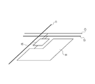
- Fig. IA is a schematic diagram showing an organic light-emitting device and a unit configured to supply electrical signals.
- FIG. IB is a schematic diagram showing a pixel circuit connected to a pixel, and signal and electrical current supply lines connected to the pixel circuit.
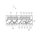
- FIG. 2 is a diagram showing a pixel circuit.
- FIG. 3 is a schematic cross-sectional view showing an organic light-emitting device and a thin film transistor underneath.
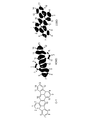
- Fig. 4 shows a structural formula of Compound C-I, electron clouds of the highest occupied molecular orbital (HOMO), and electron clouds of the lowest unoccupied molecular orbital (LUMO). Description of Embodiments
- a novel fused polycyclic compound of the present invention is a fused poly cyclic compound represented by general formula [1] below: [0018] [Chem.2]
- R 1 to R 4 is a group selected from a substituted or unsubstituted aryl group and a substituted or unsubstituted heterocyclic group, and R 1 to R 4 may be the same as or different from each other.
- the fused polycyclic compound represented by general formula [1] used in the present invention is a compound in which at least one substituted or unsubstituted aryl or heterocyclic group substitutes a particular position in a diindenochrysene backbone.
- Unsubstituted diindenochrysene has a fluorescent peak wavelength at 434 nm in a diluted solution, which is a fluorescent characteristic suitable for blue fluorescent materials, in particular, for light-emitting materials for organic light-emitting devices.
- fused polycyclic compounds have planar structures, they are sparingly soluble in organic solvents and extremely difficult to synthesize or purify. Usually, such problems are avoided by introducing various types of substituents. The effects of the position and the type of the introduced substituents on the fluorescent characteristic and thermal stability of the diindenochrysene backbone are discussed in detail below.
- Example Compound 1-1 represented by general formula [1]
- C-I diindenochrysene
- C-2 and C- 3 in toluene diluted solutions were measured.
- C-I is represented by general formula [2] with R 1 to R 15 each representing a hydrogen atom.
- C-2 is represented by general formula [2] with R 7 and R 13 each representing a 2-methyl-l-naphtyl group and all other Rs each representing a hydrogen atom.
- C-3 is represented by general formula [2] with R 6 and R 9 each representing a phenyl group, R i 2 and R 15 each representing a 3,5-di-tert-butylphenyl group, and all other Rs each representing a hydrogen atom.
- R 6 and R 9 each representing a phenyl group
- R i 2 and R 15 each representing a 3,5-di-tert-butylphenyl group
- all other Rs each representing a hydrogen atom.
- Example Compound 1-1 and C-2 both have two aryl substituents but differ in fluorescent peak wavelength by as much as 9 nm from each other.
- the molecular orbital of diindenochrysene C-I was calculated at the B3LYP/6-31G* level using a density functional theory.
- the molecular orbital calculation shows that the electron clouds of the HOMO are distributed less on the carbon atoms bonded to R 1 to R 5 and R 11 and are mainly distributed on other carbon atoms in general formula [2].
- the electron clouds of the LUMO are delocalized over the entire molecule and do not show significant polarization on the carbon atoms bonded to R 1 to R 16 in general formula [2].
- the degree of perturbation relative to the HOMO differs depending on the positions of introducing the substituents and this difference leads to the difference in fluorescent characteristics.
- the compound C-2 having aryl groups at R 7 and R 13 in general formula [2] contributes more to the resonance stabilization for the HOMO level than Example Compound 1-1 having aryl groups at R 1 and R 3 in general formula [1] and thus shows a larger increase in wavelength of the fluorescence than Example Compound 1-1.
- all of the four aryl groups occupy positions that easily perturb by the HOMO; hence, the effect of resonance stabilization worked strongly, resulting in the largest increase in wavelength.
- the positions where the substituents are to be introduced to suppress the increase in the wavelength of the fluorescence may be R 1 to R 5 and R 11 in general formula [2] above.
- Example Compound 1-1, C-I, C-2, and C-3 were fabricated and fluorescent spectra thereof were measured.
- C-I showed the largest shift in peak wavelength relative to that of the fluorescent spectrum in a diluted solution.
- the fluorescent spectrum observed was broad, extending across the green to yellow regions. This shows that in the unsubstituted compound, C-I, in a solid state, molecules are strongly associated with each other by the pi electron interactions on the fused rings, thereby achieving stabilization and the increase in wavelength of fluorescence.
- Example Compound 1-1 and C-2 both having two aryl groups shows that the effect is higher when aryl groups are introduced to R 1 and R 3 in general formula [1] than when aryl groups are introduced to R 7 and R 13 in general formula [2].
- Table 2 shows the peak wavelengths of the fluorescent spectra and CIE chromaticity of the spin-coated films and the difference in peak wavelength from that observed in toluene diluted solutions.
- Example Compound 1-1 and C- 3 have fluorescence within the blue region even when they are formed into thin films alone. Moreover, Example Compound 1-1 can realize highly pure blue fluorescence when it is dispersed.
- NPL 1 describes a synthetic example of a diindenochrysene derivative, C-4
- C-4 when C-4 is heated in a sealed tube, C-4, which had initially been a yellow solid, gradually turns brown after 180 degrees (Celsius) and melts and decomposes at 332 degrees (Celsius).
- a methyl group bonded to diindenochrysene has a benzyl hydrogen.
- a radical and an anion pair generated by dissociation of the benzyl hydrogen take a resonance structure with the fused rings of the diindenochrysene, thereby achieving significant stabilization.
- the sp 3 carbon bonded to the benzyl hydrogen is bonded to three aryl groups, the atoms are closely packed three-dimensionally and the structure is unstable.
- C-4 is highly unstable and thus easily causes pyrolysis. Such instability can lead to not only thermal instability but possibly also instability against oxygen, light, and bases. Thus, it is not preferable to use C-4 as the fluorescent material.
- Example Compound 1-1 was analyzed with a thermogravimetric/dif- ferential thermal analyzer (TG-DTA) in a nitrogen atmosphere but decomposition was not observed even at 380 degrees (Celsius).
- Example Compound 1-1 also has a benzyl hydrogen in a substituent, 2,4,6-triisopropylphenyl group.
- the carbon atom directly bonded to diindenochrysene is the sp 2 carbon in the aryl group and does not have a benzyl hydrogen.
- Example Compound 1-1 is more thermally stable than C-4.
- an aryl group and a heterocyclic group including sp 2 carbon may be the sub- stituents to be introduced to diindenochrysene.
- Diindenochrysene derivatives useful as the blue fluorescent materials are fused polycyclic compounds represented by general formula [2] where at least one of R 1 to R 5 and R 11 is a group each independently selected from a substituted or unsubstituted aryl group and a substituted or unsubstituted heterocyclic group.
- R 1 to R 5 and R 11 is a group each independently selected from a substituted or unsubstituted aryl group and a substituted or unsubstituted heterocyclic group.
- R 16 and R 10 are respectively sterically hindered by R 16 and R 10 when the substituents are introduced through coupling reactions and the like, resulting in a decrease in yield and thus are not favored. This is notable even in cases where R 16 and R 10 are hydrogen atoms.
- the diindenochrysene derivative can be a fused polycyclic compound represented by general formula [1], where at least one of R 1 to R 4 is be a group selected from a substituted or unsubstituted aryl group and a substituted or unsubstituted heterocyclic group, and R 1 to R 4 may be the same as or different from each other.
- R 2 and R 4 are moderately sterically hindered by R 6 and R 12 , respectively.
- the diindenochrysene derivative can also be a fused polycyclic compound represented by general formula [1], where R 2 and R 4 are each a hydrogen atom, at least one of R 1 and R 3 is a group selected from a substituted or unsubstituted aryl group and a substituted or unsubstituted heterocyclic group, and R 1 and R 3 may be the same as or different from each other.
- the compound represented by general formula [1] used in the present invention is a fused polycyclic compound contained in an organic compound layer of an organic light-emitting device.
- This light-emitting device at least includes a pair of electrode and the organic compound layer interposed between the pair of electrode.
- the pair of electrodes are an anode and a cathode. At least one of the anode and the cathode is transparent or semi-transparent (transmittance of about 50%) for the emission color.
- the organic compound layer is the emission layer.
- the “emission layer” refers to the very layer that emits light.
- the organic light- emitting device of the present invention may include other functional layers in addition to the emission layer. In such a case, the functional layers and the emission layer are laminated. The layer structure of the organic light-emitting device is described below.
- the organic compound layer functioning as the emission layer contains a fused poly cyclic compound represented by general formula [I].
- the emission layer may use the fused polycyclic compound represented by general formula [1] alone or as a guest material.
- the "guest material” refers to a material that defines the substantial emission color of the organic light-emitting device and is the material that can itself emit light.
- a "host material” refers to a material having a higher composition ratio than the guest material.
- the guest material has a low composition ratio in the organic light-emitting layer and the host material has a high composition ratio in the organic light-emitting layer.
- composition ratio is indicated in terms of percent by weight with respect to all components constituting the organic compound layer as the denominator.
- the fused polycyclic compound represented by general formula [1] is used as the guest
- the fused polycyclic compound content is preferably 0.1 wt% or more and 30 wt% or less with respect to the total weight of the emission layer. More preferably, the content is 0.1 wt% or more and 15 wt% or less to suppress concentration quenching. This numerical range also applies when the organic compound layer is composed of a host material and a guest material only.
- the guest material may be contained in the organic compound layer homogeneously over the entire organic compound layer or by having a concentration gradient. Alternatively, some regions of the organic compound layer may contain the guest material while other regions do not.
- the host material it not particularly limited.
- a fused polycyclic derivative can be used.
- the emission yield of the host material itself must be high and the chemical stability of the host itself must be high.
- the host material may be a chemically stable fused polycyclic derivative that exhibits high fluorescent quantum yield, e.g., fluorene derivatives, pyrene derivatives, fluoranthene derivatives, and benzofluoranthene derivatives.
- the compounds constituting the organic light-emitting device must be chemically stable.
- the fused polycyclic compound represented by general formula [1] is characterized in that because of the electron- withdrawing effect of the five-membered ring structures, the reactivity for the electrophilic reaction with singlet oxygen molecules or the like is low and the compound is thus chemically stable. Moreover, since there are two five-membered ring structures, the compound shows higher chemical stability than those having a backbone with one five-membered ring, such as fluoranthene and ben- zofluoranthene.
- the fused polycyclic compound represented by general formula [1] has electron in- jectability because of the electron-withdrawing property of the five-membered ring structures and can decrease the driving voltage when used as the material for the organic light-emitting device. Moreover, since there are two five-membered ring structures, the compound shows a higher effect of decreasing the driving voltage than those having a backbone with one five-membered ring, such as fluoranthene and ben- zofluoranthene.
- the organic light-emitting device of the present invention When the organic light-emitting device of the present invention is applied to a display, the organic light-emitting device can be used as a blue light-emitting pixel within the display region of the display.
- the fused polycyclic compound represented by general formula [1] has an emission peak at 430 to 440 nm in a diluted solution, which is the optimum position for the peak.
- the emission peaks of the blue light-emitting materials of the blue light-emitting devices be in the range of 430 to 480 nm.
- the organic light-emitting device of the present invention not only contains a blue light-emitting material having an emission peak in a range desirable for providing a blue light-emitting device.
- the organic light-emitting device of the present invention contains a blue light-emitting material having an emission peak in a range of 430 to 440 nm, which is narrower than the range of 430 to 480 nm.
- the organic compound for the organic light-emitting device may be a material having a molecular weight of 1000 or less. This is because sublimation purification can be used as the purification technique. Sublimation purification is highly effective for increasing the purity of the material.
- the organic compound contained in the organic compound layer of the organic light- emitting device of the present invention can be a fused polycyclic compound represented by general formula [1] above having a molecular weight of 1000 or less.
- the fused polycyclic compound represented by general formula [1] contained in the organic compound layer of the organic light-emitting device of the present invention is favored for its thermal stability.
- the organic compound layer of the organic light-emitting device undergoes steps such as sublimation purification and vapor deposition.
- the organic compound is subject to a temperature of 300 degrees
- Examples of the substituents (R 1 to R 4 ) of the fused polycyclic compound represented by general formula [1] are as follows.
- Examples of the substituted or unsubstituted aryl groups include, but are not limited to, a phenyl group, a naphthyl group, an indenyl group, a biphenyl group, a terphenyl group, and a fluorenyl group.
- Examples of the substituted or unsubstituted heterocyclic groups include, but are not limited to, a pyridyl group, an oxazolyl group, an oxadiazolyl group, a thiazolyl group, a thiadiazolyl group, a carbazolyl group, an acridinyl group, and a phenanthrolyl group.
- Examples of the substituent that may be included in the above-described substituents include, but are not limited to, alkyl groups such as a methyl group, an ethyl group, and a propyl group; aralkyl groups such as a benzyl group; aryl groups such as a phenyl group and a biphenyl group; heterocyclic groups such as a pyridyl group and a pyrrolyl group; amino groups such as a dimethylamino group, a diethylamino group, a dibenzylamino group, a diphenylamino group, and a ditolylamino group; alkoxy groups such as a methoxy group, an ethoxy group, a propoxy group, and a phenoxy group; a cyano group; and halogen atoms such as fluorine, chlorine, bromine, and
- fused polycyclic compound represented by general formula [1] used in the present invention include, but are not limited to, follows: [0072] [Chem.4]
- a first example of a multilayer organic light-emitting device is a structure in which an anode, an emission layer, and a cathode are sequentially layered on a substrate. This type of organic light-emitting device is useful when the emission layer itself has all of the hole transport property, the electron transport property, and the light-emitting property or when compounds having respective properties are mixed and used in the emission layer.
- a second example a multilayer organic light-emitting device is a structure in which an anode, a hole transport layer, an electron transport layer, and a cathode are sequentially layered on a substrate.
- the emission layer containing the guest material is either the hole transport layer or the electron transport layer.
- a third example of a multilayer organic light-emitting device is a structure in which an anode, a hole transport layer, an emission layer, an electron transport layer, and a cathode are sequentially layered on a substrate.
- the carrier transport function and the light-emitting function are separated.
- Compounds respectively having a hole transport property, an electron transport property, and a light-emitting property may be adequately combined and used in the device. This significantly increases the flexibility of choices of materials.
- Carriers or excitons can be effectively confined in the center emission layer to enhance the emission efficiency.
- a fourth example a multilayer organic light-emitting device is a structure in which an anode, a hole injection layer, a hole transport layer, an emission layer, an electron transport layer, and a cathode are sequentially layered on a substrate.
- This structure improves the adhesiveness between the anode and the hole transport layer and improves the hole injectability, which is effective for decreasing the voltage.
- a fifth example of a multilayer organic light-emitting device is a structure in which an anode, a hole transport layer, an emission layer, a hole/exciton-blocking layer, an electron transport layer, and a cathode are sequentially layered on a substrate.
- a layer hole/exciton-blocking layer that prevents holes or excitons from reaching the cathode is interposed between the emission layer and the electron transport layer. Since a compound having a significantly high ionization potential is used in the hole/exciton-blocking layer, the emission efficiency can be effectively enhanced.
- the first to fifth examples of the multilayer devices are merely exemplary basic device structures and do not limit the structure of the organic light-emitting device of this invention.
- various other layer structures can be employed such as providing an insulating layer at the interface between an electrode and an organic layer, providing an adhesive layer or an optical interference layer, designing the hole transport layer to be made up of two layers with different ionization potentials.
- the organic compound layer of the organic light-emitting device of the present invention may contain a low-molecular- weight or polymer hole or electron transport compound in addition to the fused polycyclic compound represented by general formula [1] if needed.
- Hole injection/transport materials used in the hole injection layer and the hole transport layer may have a high hole mobility so that holes can be easily injected from the anode and the injected holes can be transferred to the emission layer.
- Examples of the low-molecular- weight and polymer materials having hole injection/ transport functions include, but are not limited to, triarylamine derivatives, phenylenediamine derivatives, triazole derivatives, oxadiazole derivatives, imidazole derivatives, pyrazoline derivatives, pyrazolone derivatives, oxazole derivatives, fluorenone derivatives, hydrazone derivatives, stilbene derivatives, phthalocyanine derivatives, porphyrin derivatives, poly(vinyl carbazole), polysilylene, polythiophene, and other electrically conductive polymers.
- the hole injection/transport material used in the electron injection layer and/or electron transport layer can be adequately selected from those that allow easy injection of electrons from the cathode and transport the injected electrons to the emission layer.
- a material is selected by considering the balance with the carrier mobility of the hole transport material and the like.
- Examples of the material having the electron injection/ transport function include, but are not limited to, oxadiazole derivatives, oxazole derivatives, thiazole derivatives, thiadiazole derivatives, pyrazine derivatives, triazole derivatives, triazine derivatives, perylene derivatives, quinoline derivatives, quinoxaline derivatives, fluorenone derivatives, anthrone derivatives, phenanthroline derivatives, and organometal complexes.
- the organic compound layer containing the fused polycyclic compound represented by general formula [1] of the present invention and layers composed of other organic compounds in the organic light-emitting device of the present invention are formed by the following methods: vacuum vapor deposition, ionization deposition, sputtering, plasma-enhanced deposition, and various existing coating techniques (e.g., spin- coating, dipping, casting, a Langmuir-Blodgett technique, and ink-jet) that involve dissolving the compounds in adequate solvents.
- various existing coating techniques e.g., spin- coating, dipping, casting, a Langmuir-Blodgett technique, and ink-jet
- the binder resin may be selected from a wide range of binder resins.
- the binder resin include, but are not limited to, polyvinyl carbazole resin, polycarbonate resin, polyester resin, polyarylate resin, polystyrene resin, ABS resin, polybutadiene resin, polyurethane resin, acryl resin, methacryl resin, butyral resin, polyvinyl acetal resin, polyamide resin, polyimide resin, polyethylene resin, polyether sulfone resin, diallyl phthalate resin, phenol resin, epoxy resin, silicone resin, polysulfone resin, and urea resin.
- binder resins can be used alone as a homopolymer or in combination as a copolymer. If needed, additives such as a plasticizer, an antioxidant, and a UV absorber may be used in combination.
- the anode material may be a material having a work function as high as possible.
- Examples of such a material include, but are not limited to, single metals such as gold, platinum, silver, copper, nickel, palladium, cobalt, selenium, vanadium, and tungsten, and their alloys; and metal oxides such as tin oxide, zinc oxide, indium oxide, indium tin oxide (ITO), and zinc indium oxide.
- Electrically conductive polymers such as polyaniline, polypyrrole, polythiophene, polyphenylene sulfide, and the like can also be used. These electrode substances may be used alone or in combination.
- the anode may have a single-layer structure or a multilayer structure.
- the cathode material may be a material having a small work function.
- Examples of such a material include single metals such as lithium, sodium, potassium, cesium, calcium, magnesium, aluminum, indium, ruthenium, titanium, manganese, yttrium, silver, lead, tin, and chromium; and alloys such as lithium-indium, sodium- potassium, magnesium- silver, aluminum-lithium, aluminum-magnesium, and magnesium-indium.
- Metal oxides such as indium tin oxide (ITO) can also be used. These electrode substances may be used alone or in combination.
- the cathode may have a single-layer structure or a multilayer structure.
- the substrate used in the organic light-emitting device of the present invention is not particularly limited.
- an opaque substrate such as a metal substrate or a ceramic substrate, or a transparent substrate such as a glass substrate, a quartz substrate, and a plastic sheet may be used.
- a color filter film, a fluorescence color conversion filter film, a dielectric reflective film, or the like may be formed on the substrate to control the color of emission.
- a protective layer or a sealing layer may be provided to the fabricated device in order to prevent the device from contacting oxygen, moisture, and the like.
- Examples of the protective layer include inorganic material films such as diamond thin films and metal oxide and metal nitride films; polymeric films of fluorocarbon resin, polyethylene, silicone resin, and polystyrene resin; and films of photocurable resin.
- the device may be covered with glass, a gas-impermeable film, a metal, or the like and packaged with an adequate sealing resin.
- a bottom- emission structure (light is output from the substrate side) or a top-emission structure (light is output from the side opposite the substrate) is applicable.
- the organic light-emitting device of the present invention can be applied to products that require energy saving and high luminance. Examples of the application include light sources of display apparatuses such as PC monitors and televisions, lighting apparatuses, and printers, and backlights for liquid crystal display apparatuses.
- the organic light-emitting device of the present invention may be used as a pixel in a finder, which is a display section, of an image-capturing apparatus including a lens, a photo detector, and the like, i.e., a digital still camera or a digital video camera.
- the organic light-emitting device of the present invention can replace the laser light source unit of widely used laser beam printers.
- Organic light-emitting devices that can be addressed independently may be arranged on an array, and an image (latent image) is formed by conducting exposure of the photosensitive drum. In such a case, the volume of the apparatus can be significantly reduced.
- a color filter film, a fluorescence color conversion filter film, a dielectric reflective film, or the like may be formed on the substrate to control the color of emission.
- a thin film transistor may be formed on the substrate and the device can be made to connect to the TFT. It is also possible to form a matrix on a substrate to form a device and use the device for lighting.
- This display apparatus includes the organic light-emitting device of the present invention and a unit configured to supply electrical signals to the organic light-emitting device.
- the display apparatus of the present invention is described in detail below by taking an active matrix system as an example with reference to the drawings.
- Fig. IA is a schematic diagram illustrating an example of configuration of a display apparatus according to one embodiment.
- the display apparatus includes the organic light-emitting device of the present invention and a unit configured to supply electrical signals to the organic light-emitting device of the present invention.
- Fig. IB is a schematic diagram illustrating a pixel circuit connected to a pixel, and signal and electrical current supply lines connected to the pixel circuit.
- the unit configured to supply electrical signals to the organic light-emitting device of the present invention includes a scan signal driver 11, a data signal driver 12, and an electrical current supply source 13 in Fig. IA and a pixel circuit 15 in Fig. IB.
- a display apparatus 1 shown in Fig. IA includes the scan signal driver 11, the data signal driver 12, and the electrical current supply source 13 which are respectively connected to gate selection lines G, data signal lines I, and electrical current supply lines C.
- Pixel circuits 15 are arranged at intersections of the gate selection lines G and the data signal lines I, as shown in Fig. IB.
- One pixel 14 constituted by the organic light-emitting device of the present invention is provided for each corresponding pixel circuit 15.
- the pixel 14 is an organic light-emitting device.
- the organic light-emitting device is illustrated as the emission point.
- Upper electrodes of the organic light-emitting devices may be formed as a common upper electrode for all of the organic light-emitting devices. Of course, the upper electrodes of the respective organic light-emitting devices may be formed separately.
- the scan signal driver 11 sequentially selects gate selection lines Gl, G2, G3, .. and Gn, in synchronization with which image signals are applied to the pixel circuits 15 via one of data signal lines II, 12, 13, .. and In from the data signal driver 12.
- Fig. 2 is a circuit diagram showing a circuit configuring one pixel in the display apparatus 1 shown in Fig. IA.
- a second thin film transistor (TFT) 23 controls the electrical current for causing an organic light- emitting device 24 to emit light.
- TFT thin film transistor
- a selection signal is applied to a gate selection line Gi
- the first TFT 21 is turned ON
- an image signal Ii is supplied to a capacitor 22, and a gate voltage of the second TFT 23 is thereby determined.
- An electrical current is supplied to the organic light-emitting device 24 from an electrical current supply line Ci according to the gate voltage of the second TFT 23.
- the gate potential of the second TFT 23 is retained in the capacitor 22 until the first TFT 21 is scanned and selected next. Accordingly, the electric current keeps flowing in the organic light-emitting device 24 until the next time scanning is performed. As a result, the organic light-emitting device 24 keeps emitting light during one frame period.
- the organic light-emitting device of the present invention can be used in a voltage- write display apparatus in which the voltage between the electrodes of the organic light-emitting device 24 is controlled by a thin film transistor.
- FIG. 3 is a schematic view showing one example of a cross-sectional structure of a
- TFT substrate used in the display apparatus shown in Fig. IA The detailed structure is described below by taking a method for making the TFT substrate as an example.
- a moisture-proof film 32 for protecting components (TFT or organic layer) formed thereon is formed on a substrate 31 composed of glass or the like by coating. Silicon oxide or a complex of silicon oxide and silicon nitride is used to form the moisture-proof film 32. Next, a metal film of Cr or the like is formed by sputtering and patterned into a particular circuit shape to form a gate electrode 33.
- a film of silicon oxide or the like is formed by plasma-enhanced CVD or catalytic chemical vapor deposition (cat-CVD) and patterned to form a gate insulating film 34.
- a silicon film is formed by plasma-enhanced CVD or the like (annealing at a temperature of 290 degrees (Celsius) or more if necessary) and patterned according to a circuit shape to form a semiconductor layer 35.
- a drain electrode 36 and a source electrode 37 are formed on the semiconductor layer 35 to form a TFT element 38. As a result, a circuit as shown in Fig. 2 is formed. Next, an insulating film 39 is formed on the TFT element 38. A contact hole (through hole) 310 is formed to connect a metal anode 311 for the organic light-emitting device to the source electrode 37.
- a multilayer or single-layer organic layer 312 and a cathode 313 are sequentially layered on the anode 311. As a result, the display apparatus 3 is obtained.
- a first protective layer 314 and a second protective layer 315 may be provided to prevent deterioration of the organic light-emitting device.
- the switching element of the display apparatus described above is not particularly limited, and the display apparatus can be applied even with a single crystal silicon substrate, a MIM device, an a-Si device, or the like.
- An organic light-emitting display panel can be obtained by sequentially layering a single-layer or multilayer organic emission layer and a cathode layer on the ITO electrode. When the display panel using the organic compound of the present invention is driven, high-quality images can be displayed stably over a long time.
- a bottom- emission structure (light is output from the substrate side) or a top-emission structure (light is output from the side opposite the substrate) is applicable.
- Example Compound 1-1 which is one example of the fused poly cyclic compound represented by general formula [1] of the present invention, can be produced by the method described below, for example.
- intermediate mixture 3 [0127] In a nitrogen atmosphere, intermediate mixture 2 (0.900 g, 1.42 mmol) was dissolved in dichloromethane (5 ml), 0.100 g of iron powder was added thereto, and the resulting mixture was ice-cooled to 0 degrees (Celsius). Subsequently, 7.3 ml of a 2 vol% dichloromethane solution of bromine was added thereto dropwise, and the resulting reaction solution was returned to room temperature and stirred for 2 hours. Chloroform and a saturated aqueous sodium thiosulfate solution were added thereto and the resulting mixture was stirred until the color of bromine was vanished.
- intermediate 4 (0.255 g, 0.312 mmol) was dissolved in pyridine (5 ml) and the resulting solution was ice-cooled to 0 degrees (Celsius).
- Example Compound 1-1 was obtained as a yellow solid.
- Matrix-assisted laser desorption/ionization time-of- flight mass spectroscopy confirmed M + of this compound at 780.5.
- the fluorescent spectrum of a toluene solution containing Example Compound 1-1 at a concentration of 1 x 10 ⁇ 5 mol/1 was measured with F-4500 produced by Hitachi Ltd., at an excitation wavelength of 370 nm.
- the fluorescent peak wavelength is shown in Table 1 above.
- Example Compound 1-1 at a concentration of 0.1 wt% was also prepared.
- the solution was dropped onto a glass plate and spin- coating was conducted first for 10 seconds at 500 rpm and then for 40 seconds at 1000 rpm to form a film.
- C-I can be synthesized as in sections (4), (5), and (6) in Production Example 1 except that 6,12-dibromochrysene was used instead of intermediate mixture 3 in (4) of Production Example 1.
- An organic light-emitting device was produced by the following method.
- An ITO film 120 nm in thickness and serving as the anode was sputter-deposited on a glass substrate and this glass substrate was used as a transparent conductive supporting substrate.
- the substrate was sequentially ultrasonically washed with acetone and isopropyl alcohol (IPA) and washed with pure water, followed by drying.
- the substrate was further washed with UV/ozone so that it can be used as the transparent conductive supporting substrate.
- Compound A represented by the structural formula below was used as the hole transport material and a chloroform solution of compound A at a concentration of 0.1 wt% was prepared.
- the solution was dropped onto the ITO electrode and spin-coating was conducted first for 10 seconds at 500 rpm and then for 40 seconds at 1000 rpm to form a film.
- 2,9-bis[2-(9,9'-dimethylfluorenyl)]-l,10-phenanthroline was vacuum vapor-deposited to form a film having a thickness of 30 nm.
- the degree of vacuum during the deposition was 1.0 X IO 4 Pa and the deposition rate was 0.1 nm/sec or more and 0.2 nm/ sec or less.
- lithium fluoride LiF
- an aluminum film serving as an electron injection electrode and having a thickness of 100 nm was formed thereon by vacuum vapor deposition to produce an organic light-emitting device.
- the degree of vacuum during the deposition was 1.0 X IO 4 Pa and the deposition rates were 0.01 nm/sec for lithium fluoride and 0.5 nm/sec or more and 1.0 nm/sec or less for aluminum.
- the obtained organic light-emitting device was covered with a protective glass plate in a dry air atmosphere to prevent device deterioration by moisture adsorption and sealed with an acryl resin adhesive.
Landscapes
- Chemical & Material Sciences (AREA)
- Organic Chemistry (AREA)
- Physics & Mathematics (AREA)
- Spectroscopy & Molecular Physics (AREA)
- Engineering & Computer Science (AREA)
- Materials Engineering (AREA)
- Optics & Photonics (AREA)
- Electroluminescent Light Sources (AREA)
- Organic Low-Molecular-Weight Compounds And Preparation Thereof (AREA)
Priority Applications (4)
| Application Number | Priority Date | Filing Date | Title |
|---|---|---|---|
| CN2010800153454A CN102365253A (zh) | 2009-04-08 | 2010-03-29 | 新型稠合多环化合物和包括其的有机发光器件 |
| EP10761368.9A EP2417085A4 (en) | 2009-04-08 | 2010-03-29 | NEW CONDENSED POLYCYCLIC COMPOUND AND ORGANIC LIGHT-EMITTING DEVICE USING THIS LINK |
| US13/259,983 US20120013700A1 (en) | 2009-04-08 | 2010-03-29 | Novel fused polycyclic compound and organic light-emitting device including the same |
| KR1020117025828A KR101340156B1 (ko) | 2009-04-08 | 2010-03-29 | 신규 축합 다환 화합물 및 이를 포함하는 유기 발광 소자 |
Applications Claiming Priority (2)
| Application Number | Priority Date | Filing Date | Title |
|---|---|---|---|
| JP2009-094100 | 2009-04-08 | ||
| JP2009094100A JP5495606B2 (ja) | 2009-04-08 | 2009-04-08 | 新規縮合多環化合物およびそれを有する有機発光素子 |
Publications (1)
| Publication Number | Publication Date |
|---|---|
| WO2010116661A1 true WO2010116661A1 (en) | 2010-10-14 |
Family
ID=42935961
Family Applications (1)
| Application Number | Title | Priority Date | Filing Date |
|---|---|---|---|
| PCT/JP2010/002241 Ceased WO2010116661A1 (en) | 2009-04-08 | 2010-03-29 | Novel fused polycyclic compound and organic light-emitting device including the same |
Country Status (6)
| Country | Link |
|---|---|
| US (1) | US20120013700A1 (enExample) |
| EP (1) | EP2417085A4 (enExample) |
| JP (1) | JP5495606B2 (enExample) |
| KR (1) | KR101340156B1 (enExample) |
| CN (1) | CN102365253A (enExample) |
| WO (1) | WO2010116661A1 (enExample) |
Cited By (1)
| Publication number | Priority date | Publication date | Assignee | Title |
|---|---|---|---|---|
| WO2014054552A1 (en) * | 2012-10-02 | 2014-04-10 | Canon Kabushiki Kaisha | Novel organic compound and organic light-emitting device and display apparatus having the same |
Families Citing this family (2)
| Publication number | Priority date | Publication date | Assignee | Title |
|---|---|---|---|---|
| US9379350B2 (en) * | 2012-05-22 | 2016-06-28 | Electronics And Telecommunications Research Institute | Dual mode display apparatus and method of manufacturing the same |
| CN110078681B (zh) * | 2019-05-20 | 2020-10-13 | 武汉华星光电半导体显示技术有限公司 | 有机发光材料及其制备方法、有机发光器件 |
Citations (3)
| Publication number | Priority date | Publication date | Assignee | Title |
|---|---|---|---|---|
| WO2008120808A1 (en) | 2007-04-02 | 2008-10-09 | Canon Kabushiki Kaisha | Condensed ring aromatic compound for organic light-emitting device and organic light-emitting device having the same |
| WO2008120806A1 (en) | 2007-04-02 | 2008-10-09 | Canon Kabushiki Kaisha | Novel condensed ring aromatic compound and organic light-emitting device having the same |
| WO2009123344A1 (en) * | 2008-04-01 | 2009-10-08 | Canon Kabushiki Kaisha | Organic light-emitting device |
Family Cites Families (7)
| Publication number | Priority date | Publication date | Assignee | Title |
|---|---|---|---|---|
| US6627333B2 (en) * | 2001-08-15 | 2003-09-30 | Eastman Kodak Company | White organic light-emitting devices with improved efficiency |
| KR100714513B1 (ko) * | 2001-09-07 | 2007-05-07 | 마츠시타 덴끼 산교 가부시키가이샤 | El 표시 장치, 전자 표시 기기 및 el 표시 장치의 구동 회로 |
| JP3902981B2 (ja) * | 2002-06-04 | 2007-04-11 | キヤノン株式会社 | 有機発光素子及び表示装置 |
| US6830833B2 (en) * | 2002-12-03 | 2004-12-14 | Canon Kabushiki Kaisha | Organic light-emitting device based on fused conjugated compounds |
| JP2005302667A (ja) * | 2004-04-15 | 2005-10-27 | Idemitsu Kosan Co Ltd | 有機エレクトロルミネッセンス素子 |
| WO2008012806A1 (en) | 2006-07-25 | 2008-01-31 | A.R.I. Flow Control Accessories Ltd | Liquid purge valve |
| TWI412528B (zh) * | 2007-06-08 | 2013-10-21 | Solvay | 發光材料 |
-
2009
- 2009-04-08 JP JP2009094100A patent/JP5495606B2/ja not_active Expired - Fee Related
-
2010
- 2010-03-29 WO PCT/JP2010/002241 patent/WO2010116661A1/en not_active Ceased
- 2010-03-29 EP EP10761368.9A patent/EP2417085A4/en not_active Withdrawn
- 2010-03-29 CN CN2010800153454A patent/CN102365253A/zh active Pending
- 2010-03-29 KR KR1020117025828A patent/KR101340156B1/ko not_active Expired - Fee Related
- 2010-03-29 US US13/259,983 patent/US20120013700A1/en not_active Abandoned
Patent Citations (3)
| Publication number | Priority date | Publication date | Assignee | Title |
|---|---|---|---|---|
| WO2008120808A1 (en) | 2007-04-02 | 2008-10-09 | Canon Kabushiki Kaisha | Condensed ring aromatic compound for organic light-emitting device and organic light-emitting device having the same |
| WO2008120806A1 (en) | 2007-04-02 | 2008-10-09 | Canon Kabushiki Kaisha | Novel condensed ring aromatic compound and organic light-emitting device having the same |
| WO2009123344A1 (en) * | 2008-04-01 | 2009-10-08 | Canon Kabushiki Kaisha | Organic light-emitting device |
Non-Patent Citations (1)
| Title |
|---|
| See also references of EP2417085A4 |
Cited By (6)
| Publication number | Priority date | Publication date | Assignee | Title |
|---|---|---|---|---|
| WO2014054552A1 (en) * | 2012-10-02 | 2014-04-10 | Canon Kabushiki Kaisha | Novel organic compound and organic light-emitting device and display apparatus having the same |
| JP2014073966A (ja) * | 2012-10-02 | 2014-04-24 | Canon Inc | 新規有機化合物、それを有する有機発光素子及び表示装置 |
| CN104703952A (zh) * | 2012-10-02 | 2015-06-10 | 佳能株式会社 | 新型有机化合物和具有该有机化合物的有机发光器件和显示装置 |
| CN104703952B (zh) * | 2012-10-02 | 2016-10-05 | 佳能株式会社 | 新型有机化合物和具有该有机化合物的有机发光器件和显示装置 |
| US9812646B2 (en) | 2012-10-02 | 2017-11-07 | Canon Kabushiki Kaisha | Organic compound and organic light-emitting device and display apparatus having the same |
| KR101802618B1 (ko) * | 2012-10-02 | 2017-11-28 | 캐논 가부시끼가이샤 | 신규 유기 화합물 및 그를 갖는 유기 발광 소자 및 표시 장치 |
Also Published As
| Publication number | Publication date |
|---|---|
| EP2417085A1 (en) | 2012-02-15 |
| JP2010241755A (ja) | 2010-10-28 |
| KR101340156B1 (ko) | 2013-12-10 |
| US20120013700A1 (en) | 2012-01-19 |
| KR20120003925A (ko) | 2012-01-11 |
| CN102365253A (zh) | 2012-02-29 |
| EP2417085A4 (en) | 2015-03-18 |
| JP5495606B2 (ja) | 2014-05-21 |
Similar Documents
| Publication | Publication Date | Title |
|---|---|---|
| EP2243761B1 (en) | Phenanthrene derivatives, light-emitting device and image display apparatus using the same | |
| WO2010082621A1 (ja) | 有機電界発光素子 | |
| CN104703952B (zh) | 新型有机化合物和具有该有机化合物的有机发光器件和显示装置 | |
| EP2379472B1 (en) | Novel organic compound | |
| WO2012002221A1 (ja) | 発光素子用材料及び発光素子 | |
| EP2635561A1 (en) | Xanthone compound and organic light-emitting device including the same | |
| EP2338185A1 (en) | Organic light-emitting device | |
| KR20130098413A (ko) | 퀴놀리노[3,2,1-kl]페녹사진 화합물과 이를 사용한 유기 발광 소자 및 조명 장치 | |
| KR101388809B1 (ko) | 신규 유기 화합물 및 유기 발광 소자 | |
| JP5760217B2 (ja) | 有機金属錯体及びこれを用いた有機発光素子 | |
| JP5783879B2 (ja) | 新規有機化合物および有機発光素子 | |
| WO2010116661A1 (en) | Novel fused polycyclic compound and organic light-emitting device including the same | |
| KR101523153B1 (ko) | 페난트렌 화합물 및 이를 사용한 유기 발광 디바이스 | |
| JP5836771B2 (ja) | 新規有機化合物およびそれを有する有機発光素子 | |
| JP2013049651A (ja) | 縮合多環化合物及びそれを有する有機発光素子 | |
| JP5534705B2 (ja) | 新規縮合多環化合物および有機発光素子 |
Legal Events
| Date | Code | Title | Description |
|---|---|---|---|
| WWE | Wipo information: entry into national phase |
Ref document number: 201080015345.4 Country of ref document: CN |
|
| 121 | Ep: the epo has been informed by wipo that ep was designated in this application |
Ref document number: 10761368 Country of ref document: EP Kind code of ref document: A1 |
|
| REEP | Request for entry into the european phase |
Ref document number: 2010761368 Country of ref document: EP |
|
| WWE | Wipo information: entry into national phase |
Ref document number: 2010761368 Country of ref document: EP |
|
| WWE | Wipo information: entry into national phase |
Ref document number: 13259983 Country of ref document: US |
|
| NENP | Non-entry into the national phase |
Ref country code: DE |
|
| ENP | Entry into the national phase |
Ref document number: 20117025828 Country of ref document: KR Kind code of ref document: A |