US6830833B2 - Organic light-emitting device based on fused conjugated compounds - Google Patents
Organic light-emitting device based on fused conjugated compounds Download PDFInfo
- Publication number
- US6830833B2 US6830833B2 US10/308,099 US30809902A US6830833B2 US 6830833 B2 US6830833 B2 US 6830833B2 US 30809902 A US30809902 A US 30809902A US 6830833 B2 US6830833 B2 US 6830833B2
- Authority
- US
- United States
- Prior art keywords
- fused
- organic light
- emitting device
- compound
- aromatic ring
- Prior art date
- Legal status (The legal status is an assumption and is not a legal conclusion. Google has not performed a legal analysis and makes no representation as to the accuracy of the status listed.)
- Expired - Fee Related, expires
Links
- 0 [1*]C1=C([9*])C2=C(C([6*])=C1[5*])C1=C([7*])C([8*])=C([2*])C([10*])=C1C1=C2C2=C(C([14*])=C([13*])C([3*])=C2[11*])C2=C([15*])C([16*])=C([4*])C([12*])=C21 Chemical compound [1*]C1=C([9*])C2=C(C([6*])=C1[5*])C1=C([7*])C([8*])=C([2*])C([10*])=C1C1=C2C2=C(C([14*])=C([13*])C([3*])=C2[11*])C2=C([15*])C([16*])=C([4*])C([12*])=C21 0.000 description 7
- YXYNZFVHBIGOQP-UBJMFZBRSA-N C/C=C/C1=CC=CC=C1.C=CC1=CC=C(C)C=C1.C=CC1=CC=C(N(C)C2=CC=C3C4=CC=CC=C4C(C)(C)C3=C2)C=C1.C=CC1=CC=C(N(C)C2=CC=CC3=C2C=CC=C3)C=C1.C=CC1=CC=C(N(C)C2=CC=CC=C2)C=C1.C=C[Si](C)(C)C.C=C[Si](C)(C1=CC=CC=C1)C1=CC=CC=C1.CC1=CC=C(C(=O)/C=C/C2=CC=CC=C2)C=C1.CN(C1=CC=CC=C1)C1=CC=C2C3=CC=CC=C3C(C)(C)C2=C1.CN(C1=CC=CC=C1)C1=CC=CC2=C1C=CC=C2.CN(C1=CC=CC=C1)C1=CC=CC=C1.C[SiH](C)C Chemical compound C/C=C/C1=CC=CC=C1.C=CC1=CC=C(C)C=C1.C=CC1=CC=C(N(C)C2=CC=C3C4=CC=CC=C4C(C)(C)C3=C2)C=C1.C=CC1=CC=C(N(C)C2=CC=CC3=C2C=CC=C3)C=C1.C=CC1=CC=C(N(C)C2=CC=CC=C2)C=C1.C=C[Si](C)(C)C.C=C[Si](C)(C1=CC=CC=C1)C1=CC=CC=C1.CC1=CC=C(C(=O)/C=C/C2=CC=CC=C2)C=C1.CN(C1=CC=CC=C1)C1=CC=C2C3=CC=CC=C3C(C)(C)C2=C1.CN(C1=CC=CC=C1)C1=CC=CC2=C1C=CC=C2.CN(C1=CC=CC=C1)C1=CC=CC=C1.C[SiH](C)C YXYNZFVHBIGOQP-UBJMFZBRSA-N 0.000 description 5
- DTOQKESKMCVFDO-UHFFFAOYSA-N CC1=C2C=CC3=C4C(=CC=C3)/C=C\C(=C24)C=C1.CC1=C2C=CC=CC2=CC2=C1C=CC=C2.CC1=C2C=CC=CC2=CC=C1.CC1=C2C=CC=NC2=CC=C1.CC1=CC(C(F)(F)F)=CC(C(F)(F)F)=C1.CC1=CC2=C(C=CC=C2)C2=C1C=CC=C2.CC1=CC=C(C2=CC=CC=C2)C=C1.CC1=CC=C2COCC2=C1.CC1=CC=CC=C1.CC1=CC=CC=N1.CC1=CC=CS1.CC1=CC=NC=C1.CC1=NN=C(C2=CC=CC=C2)N1C1=CC=CC=C1.CC1=NN=C(C2=CC=CC=C2)O1.CN(C1=CC=C2C3=CC=CC=C3C(C)(C)C2=C1)C1=CC2=C(C=C1)C1=C(C=CC=C1)C2(C)C.CN1C2=C(C=CC=C2)C2=C/C=C/C=C\21.COC1=CC=C(C)C=C1 Chemical compound CC1=C2C=CC3=C4C(=CC=C3)/C=C\C(=C24)C=C1.CC1=C2C=CC=CC2=CC2=C1C=CC=C2.CC1=C2C=CC=CC2=CC=C1.CC1=C2C=CC=NC2=CC=C1.CC1=CC(C(F)(F)F)=CC(C(F)(F)F)=C1.CC1=CC2=C(C=CC=C2)C2=C1C=CC=C2.CC1=CC=C(C2=CC=CC=C2)C=C1.CC1=CC=C2COCC2=C1.CC1=CC=CC=C1.CC1=CC=CC=N1.CC1=CC=CS1.CC1=CC=NC=C1.CC1=NN=C(C2=CC=CC=C2)N1C1=CC=CC=C1.CC1=NN=C(C2=CC=CC=C2)O1.CN(C1=CC=C2C3=CC=CC=C3C(C)(C)C2=C1)C1=CC2=C(C=C1)C1=C(C=CC=C1)C2(C)C.CN1C2=C(C=CC=C2)C2=C/C=C/C=C\21.COC1=CC=C(C)C=C1 DTOQKESKMCVFDO-UHFFFAOYSA-N 0.000 description 5
- DXUVXWNGRMRMOR-UHFFFAOYSA-N C.C=CC1=CC=C(N(C)C2=CC=CC3=C2C=CC=C3)C=C1 Chemical compound C.C=CC1=CC=C(N(C)C2=CC=CC3=C2C=CC=C3)C=C1 DXUVXWNGRMRMOR-UHFFFAOYSA-N 0.000 description 2
- VXNZUUAINFGPBY-UHFFFAOYSA-N C=CCC Chemical compound C=CCC VXNZUUAINFGPBY-UHFFFAOYSA-N 0.000 description 2
- UHVKXYXZLWLAEX-UHFFFAOYSA-N BrC1=CC2=C(C=C1)C1=CC=CC=C1C1=C2C2=CC=CC=C2C2=C1C=C(Br)C=C2.C.C.C.C.C.C.C1=CC=C2C(=C1)C1=C(C=CC=C1)C1=C2C2=C(C=CC=C2)C2=CC=CC=C21.C=CC1=CC=C(N(C2=CC3=C(C=C2)C2=CC=CC=C2C2=C3C3=CC=CC=C3C3=C2C=C(N(C2=CC=C(C=C)C=C2)C2=C4C=CC=CC4=CC=C2)C=C3)C2=CC=CC3=C2C=CC=C3)C=C1.C=CC1=CC=C(NC2=C3C=CC=CC3=CC=C2)C=C1.O=C1C2=CC=CC=C2C2=C1/C=C\C=C/2.O=S(=O)(O)C(F)(F)F.OC1(C2(O)C3=CC=CC=C3C3=C2/C=C\C=C/3)C2=CC=CC=C2C2=C1C=CC=C2 Chemical compound BrC1=CC2=C(C=C1)C1=CC=CC=C1C1=C2C2=CC=CC=C2C2=C1C=C(Br)C=C2.C.C.C.C.C.C.C1=CC=C2C(=C1)C1=C(C=CC=C1)C1=C2C2=C(C=CC=C2)C2=CC=CC=C21.C=CC1=CC=C(N(C2=CC3=C(C=C2)C2=CC=CC=C2C2=C3C3=CC=CC=C3C3=C2C=C(N(C2=CC=C(C=C)C=C2)C2=C4C=CC=CC4=CC=C2)C=C3)C2=CC=CC3=C2C=CC=C3)C=C1.C=CC1=CC=C(NC2=C3C=CC=CC3=CC=C2)C=C1.O=C1C2=CC=CC=C2C2=C1/C=C\C=C/2.O=S(=O)(O)C(F)(F)F.OC1(C2(O)C3=CC=CC=C3C3=C2/C=C\C=C/3)C2=CC=CC=C2C2=C1C=CC=C2 UHVKXYXZLWLAEX-UHFFFAOYSA-N 0.000 description 1
- GWMLKHVIVPTAFN-UHFFFAOYSA-N BrC1=CC2=C(C=C1)C1=CC=CC=C1C1=C2C2=CC=CC=C2C2=C1C=C(Br)C=C2.C.C.C=C[Si](C)(C)C1=CC2=C(C=C1)C1=CC=CC=C1C1=C2C2=CC=CC=C2C2=C1C=C([Si](C)(C)C=C)C=C2 Chemical compound BrC1=CC2=C(C=C1)C1=CC=CC=C1C1=C2C2=CC=CC=C2C2=C1C=C(Br)C=C2.C.C.C=C[Si](C)(C)C1=CC2=C(C=C1)C1=CC=CC=C1C1=C2C2=CC=CC=C2C2=C1C=C([Si](C)(C)C=C)C=C2 GWMLKHVIVPTAFN-UHFFFAOYSA-N 0.000 description 1
- NQXGRLZHLZQZEH-RCUQKECRSA-N C.C=C[Ar].C=C[Ar].[2HH].[Ar]C1CC([Ar])C1 Chemical compound C.C=C[Ar].C=C[Ar].[2HH].[Ar]C1CC([Ar])C1 NQXGRLZHLZQZEH-RCUQKECRSA-N 0.000 description 1
- HAPLKVUJRQHNAV-UHFFFAOYSA-N C1=CC=C(C2=CC=C3C(=C2)[C@]2(C4=C3C=CC(C3=CC=CC=C3)=C4)C3=C(C=CC(C4=CC=CC=C4)=C3)C3=C2/C=C(C2=CC=CC=C2)\C=C/3)C=C1 Chemical compound C1=CC=C(C2=CC=C3C(=C2)[C@]2(C4=C3C=CC(C3=CC=CC=C3)=C4)C3=C(C=CC(C4=CC=CC=C4)=C3)C3=C2/C=C(C2=CC=CC=C2)\C=C/3)C=C1 HAPLKVUJRQHNAV-UHFFFAOYSA-N 0.000 description 1
- ZNBIPPFCWSKMHR-AICLDEIISA-N [2H]/C(C)=C(\C)F Chemical compound [2H]/C(C)=C(\C)F ZNBIPPFCWSKMHR-AICLDEIISA-N 0.000 description 1
- XELCHILJXZZIAI-QYKNYGDISA-N [2H]F(C)(C)F Chemical compound [2H]F(C)(C)F XELCHILJXZZIAI-QYKNYGDISA-N 0.000 description 1
Images


Classifications
-
- H—ELECTRICITY
- H05—ELECTRIC TECHNIQUES NOT OTHERWISE PROVIDED FOR
- H05B—ELECTRIC HEATING; ELECTRIC LIGHT SOURCES NOT OTHERWISE PROVIDED FOR; CIRCUIT ARRANGEMENTS FOR ELECTRIC LIGHT SOURCES, IN GENERAL
- H05B33/00—Electroluminescent light sources
- H05B33/12—Light sources with substantially two-dimensional [2D] radiating surfaces
- H05B33/14—Light sources with substantially two-dimensional [2D] radiating surfaces characterised by the chemical or physical composition or the arrangement of the electroluminescent material, or by the simultaneous addition of the electroluminescent material in or onto the light source
-
- C—CHEMISTRY; METALLURGY
- C07—ORGANIC CHEMISTRY
- C07C—ACYCLIC OR CARBOCYCLIC COMPOUNDS
- C07C211/00—Compounds containing amino groups bound to a carbon skeleton
- C07C211/43—Compounds containing amino groups bound to a carbon skeleton having amino groups bound to carbon atoms of six-membered aromatic rings of the carbon skeleton
- C07C211/57—Compounds containing amino groups bound to a carbon skeleton having amino groups bound to carbon atoms of six-membered aromatic rings of the carbon skeleton having amino groups bound to carbon atoms of six-membered aromatic rings being part of condensed ring systems of the carbon skeleton
- C07C211/61—Compounds containing amino groups bound to a carbon skeleton having amino groups bound to carbon atoms of six-membered aromatic rings of the carbon skeleton having amino groups bound to carbon atoms of six-membered aromatic rings being part of condensed ring systems of the carbon skeleton with at least one of the condensed ring systems formed by three or more rings
-
- C—CHEMISTRY; METALLURGY
- C07—ORGANIC CHEMISTRY
- C07F—ACYCLIC, CARBOCYCLIC OR HETEROCYCLIC COMPOUNDS CONTAINING ELEMENTS OTHER THAN CARBON, HYDROGEN, HALOGEN, OXYGEN, NITROGEN, SULFUR, SELENIUM OR TELLURIUM
- C07F7/00—Compounds containing elements of Groups 4 or 14 of the Periodic Table
- C07F7/02—Silicon compounds
- C07F7/08—Compounds having one or more C—Si linkages
- C07F7/0803—Compounds with Si-C or Si-Si linkages
- C07F7/0805—Compounds with Si-C or Si-Si linkages comprising only Si, C or H atoms
-
- C—CHEMISTRY; METALLURGY
- C09—DYES; PAINTS; POLISHES; NATURAL RESINS; ADHESIVES; COMPOSITIONS NOT OTHERWISE PROVIDED FOR; APPLICATIONS OF MATERIALS NOT OTHERWISE PROVIDED FOR
- C09K—MATERIALS FOR MISCELLANEOUS APPLICATIONS, NOT PROVIDED FOR ELSEWHERE
- C09K11/00—Luminescent materials, e.g. electroluminescent or chemiluminescent
- C09K11/06—Luminescent materials, e.g. electroluminescent or chemiluminescent containing organic luminescent materials
-
- H—ELECTRICITY
- H10—SEMICONDUCTOR DEVICES; ELECTRIC SOLID-STATE DEVICES NOT OTHERWISE PROVIDED FOR
- H10K—ORGANIC ELECTRIC SOLID-STATE DEVICES
- H10K85/00—Organic materials used in the body or electrodes of devices covered by this subclass
- H10K85/40—Organosilicon compounds, e.g. TIPS pentacene
-
- H—ELECTRICITY
- H10—SEMICONDUCTOR DEVICES; ELECTRIC SOLID-STATE DEVICES NOT OTHERWISE PROVIDED FOR
- H10K—ORGANIC ELECTRIC SOLID-STATE DEVICES
- H10K85/00—Organic materials used in the body or electrodes of devices covered by this subclass
- H10K85/60—Organic compounds having low molecular weight
- H10K85/615—Polycyclic condensed aromatic hydrocarbons, e.g. anthracene
- H10K85/624—Polycyclic condensed aromatic hydrocarbons, e.g. anthracene containing six or more rings
-
- H—ELECTRICITY
- H10—SEMICONDUCTOR DEVICES; ELECTRIC SOLID-STATE DEVICES NOT OTHERWISE PROVIDED FOR
- H10K—ORGANIC ELECTRIC SOLID-STATE DEVICES
- H10K85/00—Organic materials used in the body or electrodes of devices covered by this subclass
- H10K85/60—Organic compounds having low molecular weight
- H10K85/631—Amine compounds having at least two aryl rest on at least one amine-nitrogen atom, e.g. triphenylamine
- H10K85/633—Amine compounds having at least two aryl rest on at least one amine-nitrogen atom, e.g. triphenylamine comprising polycyclic condensed aromatic hydrocarbons as substituents on the nitrogen atom
-
- C—CHEMISTRY; METALLURGY
- C07—ORGANIC CHEMISTRY
- C07C—ACYCLIC OR CARBOCYCLIC COMPOUNDS
- C07C2603/00—Systems containing at least three condensed rings
- C07C2603/02—Ortho- or ortho- and peri-condensed systems
- C07C2603/54—Ortho- or ortho- and peri-condensed systems containing more than five condensed rings
-
- C—CHEMISTRY; METALLURGY
- C09—DYES; PAINTS; POLISHES; NATURAL RESINS; ADHESIVES; COMPOSITIONS NOT OTHERWISE PROVIDED FOR; APPLICATIONS OF MATERIALS NOT OTHERWISE PROVIDED FOR
- C09K—MATERIALS FOR MISCELLANEOUS APPLICATIONS, NOT PROVIDED FOR ELSEWHERE
- C09K2211/00—Chemical nature of organic luminescent or tenebrescent compounds
- C09K2211/10—Non-macromolecular compounds
- C09K2211/1003—Carbocyclic compounds
- C09K2211/1011—Condensed systems
-
- C—CHEMISTRY; METALLURGY
- C09—DYES; PAINTS; POLISHES; NATURAL RESINS; ADHESIVES; COMPOSITIONS NOT OTHERWISE PROVIDED FOR; APPLICATIONS OF MATERIALS NOT OTHERWISE PROVIDED FOR
- C09K—MATERIALS FOR MISCELLANEOUS APPLICATIONS, NOT PROVIDED FOR ELSEWHERE
- C09K2211/00—Chemical nature of organic luminescent or tenebrescent compounds
- C09K2211/10—Non-macromolecular compounds
- C09K2211/1003—Carbocyclic compounds
- C09K2211/1014—Carbocyclic compounds bridged by heteroatoms, e.g. N, P, Si or B
-
- H—ELECTRICITY
- H10—SEMICONDUCTOR DEVICES; ELECTRIC SOLID-STATE DEVICES NOT OTHERWISE PROVIDED FOR
- H10K—ORGANIC ELECTRIC SOLID-STATE DEVICES
- H10K50/00—Organic light-emitting devices
- H10K50/10—OLEDs or polymer light-emitting diodes [PLED]
- H10K50/11—OLEDs or polymer light-emitting diodes [PLED] characterised by the electroluminescent [EL] layers
-
- H—ELECTRICITY
- H10—SEMICONDUCTOR DEVICES; ELECTRIC SOLID-STATE DEVICES NOT OTHERWISE PROVIDED FOR
- H10K—ORGANIC ELECTRIC SOLID-STATE DEVICES
- H10K50/00—Organic light-emitting devices
- H10K50/10—OLEDs or polymer light-emitting diodes [PLED]
- H10K50/14—Carrier transporting layers
-
- H—ELECTRICITY
- H10—SEMICONDUCTOR DEVICES; ELECTRIC SOLID-STATE DEVICES NOT OTHERWISE PROVIDED FOR
- H10K—ORGANIC ELECTRIC SOLID-STATE DEVICES
- H10K85/00—Organic materials used in the body or electrodes of devices covered by this subclass
- H10K85/10—Organic polymers or oligomers
- H10K85/141—Organic polymers or oligomers comprising aliphatic or olefinic chains, e.g. poly N-vinylcarbazol, PVC or PTFE
-
- Y—GENERAL TAGGING OF NEW TECHNOLOGICAL DEVELOPMENTS; GENERAL TAGGING OF CROSS-SECTIONAL TECHNOLOGIES SPANNING OVER SEVERAL SECTIONS OF THE IPC; TECHNICAL SUBJECTS COVERED BY FORMER USPC CROSS-REFERENCE ART COLLECTIONS [XRACs] AND DIGESTS
- Y10—TECHNICAL SUBJECTS COVERED BY FORMER USPC
- Y10S—TECHNICAL SUBJECTS COVERED BY FORMER USPC CROSS-REFERENCE ART COLLECTIONS [XRACs] AND DIGESTS
- Y10S428/00—Stock material or miscellaneous articles
- Y10S428/917—Electroluminescent
Definitions
- the present invention relates to an organic light emitting device (OLED) in which a fused compound or its derivatives are used as the emissive layer and/orone or more of the charge transport layers, or as a host material in an OLED.
- OLED organic light emitting device
- Electroluminescence materials are materials which are capable of radiating light on application of an electric field. The physical model for describing this effect is based on the radiative recombination of electrons and electron gaps (holes). In light-emitting diodes, the charge carriers are injected via the cathode or anode into the electroluminescence material. Electroluminescence devices comprise a luminescence material as a light-emitting layer.
- OLEDs organic light emitting devices
- a simple OLED is fabricated by sandwiching an emissive layer between an anode and a cathode.
- holes and electrons are respectively injected from the anode and cathode into the emissive layer, typically facilitated by hole transport and electron transport layers adjacent to the respective electrodes.
- the holes and electrons radiatively combine in the emissive layer and emit light.
- Improved performance can be obtained if blocking layers are provided to block against the injection of either holes or electrons from the adjoining layer and their subsequent escape from the device.
- a double-layered structure is fabricated from a combined hole-injecting and transporting layer together with a combined electron-transporting and light-emitting layer.
- a triple-layered structure is compose of a hole-injecting and transporting layer, a light-emitting layer, and an electron-injecting and transporting layer.
- these layers from a host material doped with another material designed to achieve the desired effect of the layer (for example, to achieve a hole transport effect, an electron transport effect, or an emissive effect).
- Some of these layers can be combined, such as devices which obtain electroluminescence through doping of an electron transport layer with flourescent dye materials.
- the desired material used for OLED should ideally combine the following properties: 1) Suitable conjugation to meet band gap requirements for optimal charge injection and color requirements; 2) Easy processability for thin film formation with good morphology; 3) High thermal stability; 4) Long-term stability during device operation and in storage.
- Conjugated polymer semi-conductors have attracted attention for optoelectronic applications that traditionally have been the domains of inorganic semi-conductors.
- the structural flexibility, the very low cost for processing, and the flexible thin film features of conjugated polymers make organic semi-conductive polymer devices competitive with the inorganic semi-conductors.
- Most conjugated polymers are highly luminescent, and they have attracted great attention in light-emitting device applications.
- fused aromatic compounds can basically meet the above requirements, but they have low solubility and are difficult to prepare and purify.
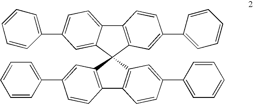
- One way to solve the solubility problem is the use of a spiro configuration.
- Spiro compounds are compounds in which two ring systems are linked via a single tetravalent atom.
- the tetravalent atom is referred to as the spiro atom.
- the basic structure of the spiro atom compound can be generally illustrated by 1, below.
- Spiro compounds are known to be luminescent and their use in light emitting devices has been suggested.
- U.S. Pat. No. 5,621,131 suggests polymers of a monomer having a spiro structure as an electroluminescent material.
- U.S. Pat. No. 5,026,894 relates to a spiro compound with a defined physical structure for use in forming semiconducting polymers with perpendicularly arranged cores.
- the compounds with perpendicularly arranged cores could then be used in memory, logic and amplification computing systems.
- Conjugated polymers comprising at least one unit based on a heterospiro framework have been alleged to have good properties including good electroluminescence, photoluminescence and high color purity.
- Spiro compounds have thus been recommended for use in electronic displays as indicated above.
- Those prior art compounds have the characteristics of high luminescence, good solubility and excellent color purity due to the prevention of intermolecular aggregation.
- Such compounds can be actually regarded as the combination of two chromophores being crossed-over each other.
- the non-conjugated spiro atom can also break up the long conjugation and lead to an inferior charge injection property.
- the good solubility can lead to deterioration over time due to changes in morphology during normal operating conditions or during conditions of elevated temperatures.
- This invention relates to electroluminescence materials suitable for use in light-emitting devices and flat-panel displays, and methods of using the same material. Particularly, this invention is aimed to improve the charge injection property of spiro-atom linked luminescent materials.
- This invention relates to electroluminescence materials suitable for use in light-emitting devices and flat-panel displays, and methods of using the same material. Particularly, this invention is aimed to improve the charge injection property of spiro-atom linked luminescent materials.
- the above compound 3 does not have a spiro atom as defined above, but rather a vinyl-linking two ring system in a non-planar geometry.
- This type of compound is a fused compound and can be regarded as a quasi-spiro compound. It has excellent hole transport properties as well as good emissive characteristics. However, its good solubility has a drawback if it is used for a hole transport layer followed with a solution thin film deposition method, such as ink-jet printing and spin-coating technique as the following solution process may damage the hole transport layer.
- this shortcoming can be overcome by cross-linking the fused compounds before or after they have been applied to the desired substrate.
- the present invention is an organic light emitting device, an organic solid state laser, and a method for producing such devices, comprising a transparent electrode; a cathode; and an active layer containing a luminescent polymer according to the present invention.
- the present invention is a photovoltaic cell, and a method for producing such a cell, comprising an active layer containing a luminescent polymer according to the present invention.
- the present invention is an electrochromic display, and a method for producing such a display, comprising an active layer containing a luminescent polymer according to the present invention.
- FIG. 1 is a representation of the three dimensional configuration of the fused conjugated compounds of the invention.
- FIG. 2 shows the electroluminescence spectrum and the photoluminescence spectrum of a compound in accordance with the present invention.
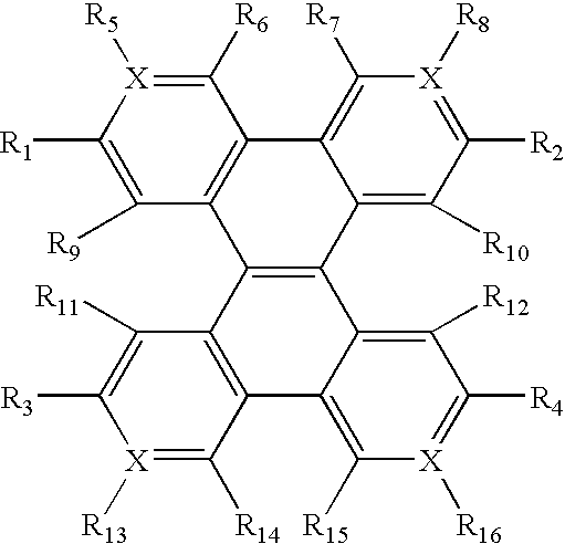
- This invention is related to electroluminescent devices wherein one of the layers is composed of a fused compound with the general formula illustrated in 4.
- the device has an advantage of good charge transport and high efficiency, as well as long-life time.
- the ring system of C1-C2-E-D, or C1-C2-G-F is a ring of 5-8 member ring containing C, O, S, N, P, Se, and a cross-linkable functional group. Due to the bond twist nature, the two-ring system is non-planar.
- FIG. 1 shows the geometry of the compound 4. Therefore, the vinyl double bond can combine a two ring system chromophore in a spiro-type configuration so as to make the two ring systems non-planar to enhance solubility (good for preparation and purification and solution processing) of the compound, and to electronically enhance charge transport ability by linking two conjugated ring systems with a conjugated double bond.
- Selecting ring constituent atoms from C, O, S, N, P, Se can adjust electron affinity to balance the charge injection and transport ability of the material. For instance, the electron negativity increases in the order CR ⁇ N ⁇ NR + ⁇ O + . Therefore, quinoline has a better electron affinity than naphthalene.
- the attachment of a cross-linkable group to the fused compound of the present invention provides a post-treatment to render the thin film insoluble. This can be beneficial to chemically fix the morphology of the formed thin film, to facilitate layer-by-layer sequential solution processing of thin films one layer on top of previous layer, and to increase thermal stability of the device.
- R 1 -R 16 is independently selected from H, D, alkyl, alkoxyl, silyl, aromatic ring, fused aromatic ring, heteroaromatic ring, fused heteroaromatic ring, diarylamino group, carbazole, and at least one of them being a crosslinkable group consisting of a vinyl double bond or an azide group.
- the compounds according to the invention have a conjugated spiro-type linkage linking two chromophores or two polymers together, and the spiro-type linkage renders the two chromophores or two polymers crossed over each other, so as to effectively prevent the intermolecular pi-conjugation system from forming an aggregate.
- the conjugated spiro system also allows electronic interaction between the two crossed systems.
- the compound expressed according to formula (5) can be used directly as a charge transport layer, as an emissive layer, or can be used as a host material in OLEDs. Assembly of such OLED's is well known to those of ordinary skill in the art.
- Fabrication of a suitable hole transport layer of the compound (5) can be accomplished through use of thermal deposition in a vacuum, or by a solution thin film deposition techniques, such as spin coating of a solution, or ink-jet printing.
- a hole-transport layer coated ITO glass substrate can be heated to a suitable temperature between 80 to 240° C. in order to induce a cross-linking reaction.
- the double bond in the compound 5 will meet with another double bond of another compound 5 molecule and via 2+2 cyclization, lead to the formation of an insoluble network which will not be damaged or altered by further processing.
- Crosslinking reaction of the chromophore under heating condition (temperature range from 150-350 C, preferably between 180-250 C).
- Fused conjugated compounds of the present invention can be synthesized in accordance with the following example:
- the compound 8 (2.098 g, 6.388 mmol) was dissolved in dichloromethane (25 ml), and catalytic iodine (16.2 mg, 0.0688 mmol) was added into the solution.
- Bromine (2.09 g, 13.09 mmol) was added into the solution within 30 min. at 0° C.
- the mixture was stirred for 18 hours, and potassium hydroxide (10 ml, 20% solution) was added into the mixture to terminate the reaction.
- the mixture was poured into methanol (300 ml) to give a white precipitate.
- the solid was filtered and washed by water (2 ⁇ 80 ml), methanol (2 ⁇ 30 ml) and dried under vacuum.
- GC/MS revealed to be the product 9 (2.733 g, 88% yield).
- the compound 9 (0.606 g, 1.357) was dissolved in anhydrous tetrahydrofuran (10 ml) and degassed. After cooling to ⁇ 70° C. (dry ice+acetone as cold bath), t BuLi (3.19 ml in 1.7 M solution in heptane, 5.43 mmol). The red solution was stirred at ⁇ 70° C. for 1.5 hours, and dimethyl vinylsilane chloride (0.327 g, 2.714 mmol) was added. The mixture was stirred and warmed to room temperature. After 14 hours stirring at room temperature, it was poured into water (300 ml). The product 12 was purified by standard silicon flash column to give yellow powder. (60% yield) The compound was characterized by FT-IR and GC/MS.
- Compound 12(15 mg) was dissolved in chloroform (0.8 ml) and the solution was spin-coated on a glass substrate to form a 30 nm thin film.
- the glass substrate was heated under vacuum to 180° C. for 4 hours to cross-link 12.
- the hole transport material 11 (8 mg) was dissolved in chloroform (1 ml) and filtered through a 0.5 ⁇ m Teflon membrane filter. The solution was spin-coated on a clean indium tin oxide glass substrate (ITO glass) to form a thin film 10 nm thick. The coated ITO glass was heated to 180° C. under vacuum for 4 hours. On top of the cross-linked 11, emissive compound 12 (15 mg in 0.8 ml chloroform) was spin-coated on top of the cross-linked 11 to form a thin film 30 nm thick of compound 12. The coated ITO substrate was then put into a vacuum deposition bell jar to deposit cathode metal layer, LiF (0.8 nm) followed with aluminum (150 nm).
- FIG. 2 shows the electroluminescence spectrum (EL) and photoluminescence spectrum (PL) of the compound 12.
Landscapes
- Chemical & Material Sciences (AREA)
- Organic Chemistry (AREA)
- Engineering & Computer Science (AREA)
- Materials Engineering (AREA)
- Physics & Mathematics (AREA)
- Spectroscopy & Molecular Physics (AREA)
- Electroluminescent Light Sources (AREA)
- Organic Low-Molecular-Weight Compounds And Preparation Thereof (AREA)
Abstract

Description


Claims (12)


Priority Applications (3)
| Application Number | Priority Date | Filing Date | Title |
|---|---|---|---|
| US10/308,099 US6830833B2 (en) | 2002-12-03 | 2002-12-03 | Organic light-emitting device based on fused conjugated compounds |
| JP2003403748A JP3880574B2 (en) | 2002-12-03 | 2003-12-02 | Organic light-emitting devices based on condensed conjugated compounds |
| CNA200310118744A CN1505179A (en) | 2002-12-03 | 2003-12-02 | Organic light-emitting device based on spiro-type conjugated compounds |
Applications Claiming Priority (1)
| Application Number | Priority Date | Filing Date | Title |
|---|---|---|---|
| US10/308,099 US6830833B2 (en) | 2002-12-03 | 2002-12-03 | Organic light-emitting device based on fused conjugated compounds |
Publications (2)
| Publication Number | Publication Date |
|---|---|
| US20040106004A1 US20040106004A1 (en) | 2004-06-03 |
| US6830833B2 true US6830833B2 (en) | 2004-12-14 |
Family
ID=32392692
Family Applications (1)
| Application Number | Title | Priority Date | Filing Date |
|---|---|---|---|
| US10/308,099 Expired - Fee Related US6830833B2 (en) | 2002-12-03 | 2002-12-03 | Organic light-emitting device based on fused conjugated compounds |
Country Status (3)
| Country | Link |
|---|---|
| US (1) | US6830833B2 (en) |
| JP (1) | JP3880574B2 (en) |
| CN (1) | CN1505179A (en) |
Cited By (3)
| Publication number | Priority date | Publication date | Assignee | Title |
|---|---|---|---|---|
| US20030039803A1 (en) * | 2000-02-09 | 2003-02-27 | Burroughes Jeremey Henley | Optoelectronic devices |
| US8592056B2 (en) | 2007-05-17 | 2013-11-26 | Semiconductor Energy Laboratory Co., Ltd. | Triazole derivative, and light-emitting element, light-emitting device, and electronic device with the use of triazole derivative |
| US10249824B2 (en) | 2012-05-03 | 2019-04-02 | Samsung Display Co., Ltd. | Condensed-cyclic compound and organic light-emitting diode comprising the same |
Families Citing this family (32)
| Publication number | Priority date | Publication date | Assignee | Title |
|---|---|---|---|---|
| US7271406B2 (en) * | 2003-04-15 | 2007-09-18 | 3M Innovative Properties Company | Electron transport agents for organic electronic devices |
| KR101807644B1 (en) * | 2008-02-27 | 2017-12-11 | 도레이 카부시키가이샤 | Luminescent element material and luminescent element |
| KR20090111915A (en) * | 2008-04-23 | 2009-10-28 | (주)그라쎌 | Novel organic light emitting compound and organic light emitting device employing the same as light emitting material |
| JP5687628B2 (en) * | 2008-11-19 | 2015-03-18 | イー・アイ・デュポン・ドウ・ヌムール・アンド・カンパニーE.I.Du Pont De Nemours And Company | Chrysene compounds for blue or green luminescence applications |
| US8531100B2 (en) * | 2008-12-22 | 2013-09-10 | E I Du Pont De Nemours And Company | Deuterated compounds for luminescent applications |
| US8759818B2 (en) * | 2009-02-27 | 2014-06-24 | E I Du Pont De Nemours And Company | Deuterated compounds for electronic applications |
| WO2010114583A1 (en) | 2009-04-03 | 2010-10-07 | E. I. Du Pont De Nemours And Company | Electroactive materials |
| JP5495606B2 (en) * | 2009-04-08 | 2014-05-21 | キヤノン株式会社 | Novel condensed polycyclic compound and organic light emitting device having the same |
| JP5685832B2 (en) * | 2009-05-29 | 2015-03-18 | Jnc株式会社 | Dibenzo [g, p] chrysene compound, light emitting layer material containing the compound, and organic electroluminescence device using the same |
| JP5567675B2 (en) * | 2009-08-13 | 2014-08-06 | イー・アイ・デュポン・ドウ・ヌムール・アンド・カンパニー | Chrysene derivative material |
| KR101117722B1 (en) * | 2009-08-28 | 2012-03-07 | 삼성모바일디스플레이주식회사 | Organic light emitting device |
| TW201114771A (en) | 2009-10-29 | 2011-05-01 | Du Pont | Deuterated compounds for electronic applications |
| US8617720B2 (en) | 2009-12-21 | 2013-12-31 | E I Du Pont De Nemours And Company | Electroactive composition and electronic device made with the composition |
| EP2588527B1 (en) | 2010-07-02 | 2017-10-25 | Nissan Chemical Industries, Ltd. | Hole transport compositions and related devices and methods (i) |
| JP5727038B2 (en) | 2010-12-20 | 2015-06-03 | イー・アイ・デュポン・ドウ・ヌムール・アンド・カンパニーE.I.Du Pont De Nemours And Company | Compositions for electronic technology applications |
| US9985215B2 (en) | 2012-03-09 | 2018-05-29 | Kyulux, Inc. | Light-emitting material, and organic light-emitting element |
| US8546617B1 (en) | 2012-03-23 | 2013-10-01 | Empire Technology Development Llc | Dioxaborinanes and uses thereof |
| US9290598B2 (en) | 2012-03-29 | 2016-03-22 | Empire Technology Development Llc | Dioxaborinane co-polymers and uses thereof |
| EP2850668B1 (en) | 2012-05-15 | 2019-11-20 | Nissan Chemical Corporation | Hole transport materials including oled applications |
| US9095141B2 (en) | 2012-07-31 | 2015-08-04 | Empire Technology Development Llc | Antifouling compositions including dioxaborinanes and uses thereof |
| JP6221029B2 (en) * | 2013-02-13 | 2017-11-01 | 黒金化成株式会社 | Novel compound, polymer using the same, curing agent and cross-linking agent |
| US10233269B2 (en) | 2013-03-29 | 2019-03-19 | Tokyo Ohka Kogyo Co., Ltd. | Compound containing structural unit derived from vinyl ether compound |
| TWI593668B (en) | 2013-03-29 | 2017-08-01 | Tokyo Ohka Kogyo Co Ltd | Compositions holding vinyl-containing compounds |
| KR101840528B1 (en) * | 2013-03-29 | 2018-03-20 | 도오꾜오까고오교 가부시끼가이샤 | Vinyl-group-containing fluorene compound |
| KR20170005413A (en) * | 2014-05-08 | 2017-01-13 | 미쯔비시 가스 케미칼 컴파니, 인코포레이티드 | Resist material, resist composition, and resist pattern formation method |
| SG11201609095VA (en) * | 2014-05-08 | 2016-12-29 | Mitsubishi Gas Chemical Co | Material for forming film for lithography, composition for forming film for lithography, film for lithography, pattern forming method and purification method |
| KR102273051B1 (en) | 2014-10-21 | 2021-07-06 | 삼성디스플레이 주식회사 | Compound for hole transporting and organic light emitting device utilizing same |
| EP3348559B1 (en) * | 2015-09-08 | 2019-11-20 | Shin-Etsu Chemical Co., Ltd. | Novel vinyl silane compound |
| JP6357673B2 (en) * | 2017-03-13 | 2018-07-18 | 黒金化成株式会社 | Novel compound, polymer using the same, curing agent and cross-linking agent |
| WO2019031605A1 (en) * | 2017-08-10 | 2019-02-14 | 東ソー株式会社 | Fused ring compound |
| EP3850024A4 (en) * | 2018-09-11 | 2022-07-06 | Greene, Tweed Technologies, Inc. | CROSSLINKING COMPOSITIONS FOR FORMING CROSSLINKED ORGANIC POLYMERS, ORGANIC POLYMERIC COMPOSITIONS, METHODS FOR FORMING THEREOF, AND MOLDED ARTICLES PRODUCED THEREOF |
| KR20220038211A (en) | 2020-09-18 | 2022-03-28 | 삼성디스플레이 주식회사 | Heterocyclic compound, hole transport composition comprising the same, light emitting device comprising the same and method for manufacturing the same, and electonic apparatus |
Citations (18)
| Publication number | Priority date | Publication date | Assignee | Title |
|---|---|---|---|---|
| US5026894A (en) | 1990-03-12 | 1991-06-25 | University Of South Carolina | Compound for use in the synthesis of semiconducting polymers with perpendicularly arranged cores and method of synthesizing said compound |
| JPH05202355A (en) | 1992-01-29 | 1993-08-10 | Sumitomo Chem Co Ltd | Organic electroluminescent device |
| US5621131A (en) | 1994-10-14 | 1997-04-15 | Hoechst Aktiengesellschaft | Conjugated polymers having spiro centers and their use as electroluminescence materials |
| US5763636A (en) | 1995-10-12 | 1998-06-09 | Hoechst Aktiengesellschaft | Polymers containing spiro atoms and methods of using the same as electroluminescence materials |
| US5840217A (en) * | 1994-04-07 | 1998-11-24 | Hoechst Aktiengesellschaft | Spiro compounds and their use as electroluminescence materials |
| US5859211A (en) | 1996-04-17 | 1999-01-12 | Hoechst Aktiengesellschaft | Conjugated polymers containing heterospiro atoms and their use as electroluminescence materials |
| US5942340A (en) | 1997-10-02 | 1999-08-24 | Xerox Corporation | Indolocarbazole electroluminescent devices |
| US5981773A (en) * | 1997-01-14 | 1999-11-09 | Ciba Specialty Chemicals Corporation | Preparation of perylene-3,4-dicarboxylic anhydrides |
| US6004685A (en) | 1997-12-23 | 1999-12-21 | Hewlett-Packard Company & The Board Of Regents Of The University Of Texas System | LED doped with periflanthene for efficient red emission |
| US6132641A (en) | 1995-12-01 | 2000-10-17 | Vantico, Inc. | Composition and support material comprising poly(9,9'-spiro-bisfluorenes) |
| US6169163B1 (en) * | 1995-07-28 | 2001-01-02 | The Dow Chemical Company | Fluorene-containing polymers and compounds useful in the preparation thereof |
| US6329082B1 (en) | 1994-11-25 | 2001-12-11 | Hoechst Aktiengesellschaft | Hetero-spiro compounds and their use as electroluminescence materials |
| US6361884B1 (en) | 1996-02-22 | 2002-03-26 | Covian Organic Semiconductor Gmbh | Partially conjugated polymers with spiro centers and their use as electro-luminescent materials |
| US6376694B1 (en) | 1998-07-09 | 2002-04-23 | Chisso Corporation | Silole derivatives and organic electroluminescent element containing the same |
| US6416887B1 (en) * | 1998-11-11 | 2002-07-09 | Kabushiki Kaisha Toyota Chuo Kenkyusho | Organic electroluminescent element |
| JP2002237384A (en) * | 2001-02-07 | 2002-08-23 | Toyota Central Res & Dev Lab Inc | Organic electroluminescent device |
| EP1363980A1 (en) * | 2001-02-26 | 2003-11-26 | Isis Innovation Limited | Luminescent polymers |
| US6664396B1 (en) * | 2002-06-27 | 2003-12-16 | Eastman Kodak Company | One step synthesis for quinacridone compounds |
-
2002
- 2002-12-03 US US10/308,099 patent/US6830833B2/en not_active Expired - Fee Related
-
2003
- 2003-12-02 JP JP2003403748A patent/JP3880574B2/en not_active Expired - Fee Related
- 2003-12-02 CN CNA200310118744A patent/CN1505179A/en active Pending
Patent Citations (18)
| Publication number | Priority date | Publication date | Assignee | Title |
|---|---|---|---|---|
| US5026894A (en) | 1990-03-12 | 1991-06-25 | University Of South Carolina | Compound for use in the synthesis of semiconducting polymers with perpendicularly arranged cores and method of synthesizing said compound |
| JPH05202355A (en) | 1992-01-29 | 1993-08-10 | Sumitomo Chem Co Ltd | Organic electroluminescent device |
| US5840217A (en) * | 1994-04-07 | 1998-11-24 | Hoechst Aktiengesellschaft | Spiro compounds and their use as electroluminescence materials |
| US5621131A (en) | 1994-10-14 | 1997-04-15 | Hoechst Aktiengesellschaft | Conjugated polymers having spiro centers and their use as electroluminescence materials |
| US6329082B1 (en) | 1994-11-25 | 2001-12-11 | Hoechst Aktiengesellschaft | Hetero-spiro compounds and their use as electroluminescence materials |
| US6169163B1 (en) * | 1995-07-28 | 2001-01-02 | The Dow Chemical Company | Fluorene-containing polymers and compounds useful in the preparation thereof |
| US5763636A (en) | 1995-10-12 | 1998-06-09 | Hoechst Aktiengesellschaft | Polymers containing spiro atoms and methods of using the same as electroluminescence materials |
| US6132641A (en) | 1995-12-01 | 2000-10-17 | Vantico, Inc. | Composition and support material comprising poly(9,9'-spiro-bisfluorenes) |
| US6361884B1 (en) | 1996-02-22 | 2002-03-26 | Covian Organic Semiconductor Gmbh | Partially conjugated polymers with spiro centers and their use as electro-luminescent materials |
| US5859211A (en) | 1996-04-17 | 1999-01-12 | Hoechst Aktiengesellschaft | Conjugated polymers containing heterospiro atoms and their use as electroluminescence materials |
| US5981773A (en) * | 1997-01-14 | 1999-11-09 | Ciba Specialty Chemicals Corporation | Preparation of perylene-3,4-dicarboxylic anhydrides |
| US5942340A (en) | 1997-10-02 | 1999-08-24 | Xerox Corporation | Indolocarbazole electroluminescent devices |
| US6004685A (en) | 1997-12-23 | 1999-12-21 | Hewlett-Packard Company & The Board Of Regents Of The University Of Texas System | LED doped with periflanthene for efficient red emission |
| US6376694B1 (en) | 1998-07-09 | 2002-04-23 | Chisso Corporation | Silole derivatives and organic electroluminescent element containing the same |
| US6416887B1 (en) * | 1998-11-11 | 2002-07-09 | Kabushiki Kaisha Toyota Chuo Kenkyusho | Organic electroluminescent element |
| JP2002237384A (en) * | 2001-02-07 | 2002-08-23 | Toyota Central Res & Dev Lab Inc | Organic electroluminescent device |
| EP1363980A1 (en) * | 2001-02-26 | 2003-11-26 | Isis Innovation Limited | Luminescent polymers |
| US6664396B1 (en) * | 2002-06-27 | 2003-12-16 | Eastman Kodak Company | One step synthesis for quinacridone compounds |
Non-Patent Citations (2)
| Title |
|---|
| Handbook of Chemistry and Physics, 62d Edition (1981-2), CRC Press, pp. C-23 through C-25. |
| U.S. Patent Application Publication No. US 2002/0048686. |
Cited By (6)
| Publication number | Priority date | Publication date | Assignee | Title |
|---|---|---|---|---|
| US20030039803A1 (en) * | 2000-02-09 | 2003-02-27 | Burroughes Jeremey Henley | Optoelectronic devices |
| US7091516B2 (en) * | 2000-02-09 | 2006-08-15 | Cambridge Display Technology Limited | Optoelectronic devices |
| US8592056B2 (en) | 2007-05-17 | 2013-11-26 | Semiconductor Energy Laboratory Co., Ltd. | Triazole derivative, and light-emitting element, light-emitting device, and electronic device with the use of triazole derivative |
| US9397299B2 (en) | 2007-05-17 | 2016-07-19 | Semiconductor Energy Laboratory Co., Ltd. | Triazole derivative, and light-emitting element, light-emitting device, and electronic device with the use of triazole derivative |
| US10790451B2 (en) | 2007-05-17 | 2020-09-29 | Semiconductor Energy Laboratory Co., Ltd. | Triazole derivative, and light-emitting element, light-emitting device, and electronic device with the use of triazole derivative |
| US10249824B2 (en) | 2012-05-03 | 2019-04-02 | Samsung Display Co., Ltd. | Condensed-cyclic compound and organic light-emitting diode comprising the same |
Also Published As
| Publication number | Publication date |
|---|---|
| US20040106004A1 (en) | 2004-06-03 |
| JP3880574B2 (en) | 2007-02-14 |
| JP2004182737A (en) | 2004-07-02 |
| CN1505179A (en) | 2004-06-16 |
Similar Documents
| Publication | Publication Date | Title |
|---|---|---|
| US6830833B2 (en) | Organic light-emitting device based on fused conjugated compounds | |
| KR100480769B1 (en) | White Electroluminescent Polymer And Organic Electroluminescent Device Using Thereof | |
| KR101311934B1 (en) | Composition for organic photoelectric device and organic photoelectric device using the same | |
| US20070116984A1 (en) | Spiro-compound for electroluminescent display device and electroluminescent display device comprising the same | |
| CN101679459B (en) | Organic metal complexes derivative and organic light emitting devices using the same | |
| CN1480012A (en) | Deuterated semiconducting organic compounds for optoelectronic devices | |
| KR100679724B1 (en) | Color-emitting compound for electroluminescent device and organic electroluminescent device comprising same | |
| US7862904B2 (en) | Organic electroluminescent element | |
| KR100351234B1 (en) | Low molecular chromophore compounds and organic electroluminescence display device comprising the same | |
| KR101297162B1 (en) | Composition for organic photoelectric device and organic photoelectric device using the same | |
| WO2006065105A1 (en) | Compounds and organic electroluminescence display device comprising the same | |
| WO2004065520A1 (en) | Light-emitting device, condensed polycyclic compound used therein and method for producing same | |
| US20070013294A1 (en) | White light-emitting electroluminescent device | |
| KR101380008B1 (en) | New anthracene derivatives and organic electronic device using the same | |
| US7951965B2 (en) | Phenanthrene derivatives and organic light-emitting diodes containing said phenanthrene derivative | |
| CN1995097B (en) | Blue electroluminescent polymer, method of preparing blue electroluminescent polymer, and organic electroluminescent device employing the same | |
| KR101350744B1 (en) | Electriluminescent polymer containing benzothiadiazole derivatives and organoelectriluminescent device emloying the same | |
| WO2021103728A1 (en) | Organic compound and organic electroluminescent device using same | |
| KR101233376B1 (en) | Organic photoelectric device and display including the same | |
| US6844088B2 (en) | Bisphenylene-spirobifluorene compounds, method for synthesizing the same, and electroluminescence material and device having the same | |
| CN107954996A (en) | Thianthrene-S, S- tetroxide derivative and preparation method and the application in organic electroluminescence device | |
| CN109585691B (en) | An organic electroluminescent device containing fluorene derivatives | |
| KR101412813B1 (en) | Organic electroluminescent polymer containing oxadiazole group and organic electroluminescent device manufactured using the same | |
| CN100366623C (en) | Light-emitting element, condensed polycyclic compound used therein, and manufacturing method thereof | |
| KR101400472B1 (en) | Organic electroluminescent polymer containing novel blue dopants and organic electroluminescent devices manufactured using the same |
Legal Events
| Date | Code | Title | Description |
|---|---|---|---|
| AS | Assignment |
Owner name: CANON KABUSHIKI KAISHA, JAPAN Free format text: ASSIGNMENT OF ASSIGNORS INTEREST;ASSIGNOR:LI, XIAO-CHANG CHARLES;REEL/FRAME:013885/0632 Effective date: 20021207 |
|
| FEPP | Fee payment procedure |
Free format text: PAYOR NUMBER ASSIGNED (ORIGINAL EVENT CODE: ASPN); ENTITY STATUS OF PATENT OWNER: LARGE ENTITY |
|
| FPAY | Fee payment |
Year of fee payment: 4 |
|
| FPAY | Fee payment |
Year of fee payment: 8 |
|
| REMI | Maintenance fee reminder mailed | ||
| LAPS | Lapse for failure to pay maintenance fees | ||
| STCH | Information on status: patent discontinuation |
Free format text: PATENT EXPIRED DUE TO NONPAYMENT OF MAINTENANCE FEES UNDER 37 CFR 1.362 |
|
| STCH | Information on status: patent discontinuation |
Free format text: PATENT EXPIRED DUE TO NONPAYMENT OF MAINTENANCE FEES UNDER 37 CFR 1.362 |
|
| FP | Lapsed due to failure to pay maintenance fee |
Effective date: 20161214 |