WO2010110099A1 - Plasma processing apparatus and method of producing amorphous silicon thin film using same - Google Patents
Plasma processing apparatus and method of producing amorphous silicon thin film using same Download PDFInfo
- Publication number
- WO2010110099A1 WO2010110099A1 PCT/JP2010/054293 JP2010054293W WO2010110099A1 WO 2010110099 A1 WO2010110099 A1 WO 2010110099A1 JP 2010054293 W JP2010054293 W JP 2010054293W WO 2010110099 A1 WO2010110099 A1 WO 2010110099A1
- Authority
- WO
- WIPO (PCT)
- Prior art keywords
- gas
- plasma
- electrode
- processing apparatus
- gas exhaust
- Prior art date
Links
- 238000012545 processing Methods 0.000 title claims abstract description 104
- 239000010409 thin film Substances 0.000 title claims abstract description 80
- 229910021417 amorphous silicon Inorganic materials 0.000 title claims abstract description 68
- 238000000034 method Methods 0.000 title abstract description 27
- 239000000758 substrate Substances 0.000 claims abstract description 102
- 230000007246 mechanism Effects 0.000 claims abstract description 31
- 238000007599 discharging Methods 0.000 claims abstract description 3
- BLRPTPMANUNPDV-UHFFFAOYSA-N Silane Chemical compound [SiH4] BLRPTPMANUNPDV-UHFFFAOYSA-N 0.000 claims description 24
- 229910000077 silane Inorganic materials 0.000 claims description 24
- 238000010438 heat treatment Methods 0.000 claims description 18
- 238000004519 manufacturing process Methods 0.000 claims description 14
- 239000002994 raw material Substances 0.000 claims description 11
- 238000005229 chemical vapour deposition Methods 0.000 claims description 9
- 229910052710 silicon Inorganic materials 0.000 claims description 6
- XUIMIQQOPSSXEZ-UHFFFAOYSA-N Silicon Chemical compound [Si] XUIMIQQOPSSXEZ-UHFFFAOYSA-N 0.000 claims description 5
- 239000010703 silicon Substances 0.000 claims description 5
- 239000007789 gas Substances 0.000 description 372
- 239000010408 film Substances 0.000 description 40
- 239000000126 substance Substances 0.000 description 24
- 238000005268 plasma chemical vapour deposition Methods 0.000 description 18
- 239000002245 particle Substances 0.000 description 11
- 230000007547 defect Effects 0.000 description 10
- 239000011521 glass Substances 0.000 description 8
- 238000001782 photodegradation Methods 0.000 description 7
- 230000015572 biosynthetic process Effects 0.000 description 6
- 238000006243 chemical reaction Methods 0.000 description 6
- 238000005755 formation reaction Methods 0.000 description 6
- 238000009832 plasma treatment Methods 0.000 description 5
- 230000008569 process Effects 0.000 description 5
- 238000000354 decomposition reaction Methods 0.000 description 4
- 239000012212 insulator Substances 0.000 description 4
- 101000701286 Pseudomonas aeruginosa (strain ATCC 15692 / DSM 22644 / CIP 104116 / JCM 14847 / LMG 12228 / 1C / PRS 101 / PAO1) Alkanesulfonate monooxygenase Proteins 0.000 description 3
- 101000983349 Solanum commersonii Osmotin-like protein OSML13 Proteins 0.000 description 3
- 230000002159 abnormal effect Effects 0.000 description 3
- 230000009471 action Effects 0.000 description 3
- 230000000052 comparative effect Effects 0.000 description 3
- 230000006872 improvement Effects 0.000 description 3
- 238000005259 measurement Methods 0.000 description 3
- 238000010248 power generation Methods 0.000 description 3
- XKRFYHLGVUSROY-UHFFFAOYSA-N Argon Chemical compound [Ar] XKRFYHLGVUSROY-UHFFFAOYSA-N 0.000 description 2
- 238000005033 Fourier transform infrared spectroscopy Methods 0.000 description 2
- UFHFLCQGNIYNRP-UHFFFAOYSA-N Hydrogen Chemical compound [H][H] UFHFLCQGNIYNRP-UHFFFAOYSA-N 0.000 description 2
- 238000009739 binding Methods 0.000 description 2
- 238000007664 blowing Methods 0.000 description 2
- 239000000470 constituent Substances 0.000 description 2
- 230000007423 decrease Effects 0.000 description 2
- 230000000694 effects Effects 0.000 description 2
- 238000005530 etching Methods 0.000 description 2
- 239000001257 hydrogen Substances 0.000 description 2
- 229910052739 hydrogen Inorganic materials 0.000 description 2
- 238000002156 mixing Methods 0.000 description 2
- 229910021421 monocrystalline silicon Inorganic materials 0.000 description 2
- 230000000149 penetrating effect Effects 0.000 description 2
- 238000002834 transmittance Methods 0.000 description 2
- 238000010521 absorption reaction Methods 0.000 description 1
- 230000002411 adverse Effects 0.000 description 1
- 238000013459 approach Methods 0.000 description 1
- 229910052786 argon Inorganic materials 0.000 description 1
- 239000006227 byproduct Substances 0.000 description 1
- 230000015556 catabolic process Effects 0.000 description 1
- 230000008859 change Effects 0.000 description 1
- 238000006731 degradation reaction Methods 0.000 description 1
- 230000006866 deterioration Effects 0.000 description 1
- 238000001312 dry etching Methods 0.000 description 1
- 230000005684 electric field Effects 0.000 description 1
- 230000007613 environmental effect Effects 0.000 description 1
- 239000010419 fine particle Substances 0.000 description 1
- 229910052736 halogen Inorganic materials 0.000 description 1
- 150000002367 halogens Chemical class 0.000 description 1
- 230000010354 integration Effects 0.000 description 1
- 238000012423 maintenance Methods 0.000 description 1
- 239000000463 material Substances 0.000 description 1
- 230000004048 modification Effects 0.000 description 1
- 238000012986 modification Methods 0.000 description 1
- 230000000717 retained effect Effects 0.000 description 1
- 230000007847 structural defect Effects 0.000 description 1
- 230000001629 suppression Effects 0.000 description 1
- 238000004381 surface treatment Methods 0.000 description 1
Images


Classifications
-
- C—CHEMISTRY; METALLURGY
- C23—COATING METALLIC MATERIAL; COATING MATERIAL WITH METALLIC MATERIAL; CHEMICAL SURFACE TREATMENT; DIFFUSION TREATMENT OF METALLIC MATERIAL; COATING BY VACUUM EVAPORATION, BY SPUTTERING, BY ION IMPLANTATION OR BY CHEMICAL VAPOUR DEPOSITION, IN GENERAL; INHIBITING CORROSION OF METALLIC MATERIAL OR INCRUSTATION IN GENERAL
- C23C—COATING METALLIC MATERIAL; COATING MATERIAL WITH METALLIC MATERIAL; SURFACE TREATMENT OF METALLIC MATERIAL BY DIFFUSION INTO THE SURFACE, BY CHEMICAL CONVERSION OR SUBSTITUTION; COATING BY VACUUM EVAPORATION, BY SPUTTERING, BY ION IMPLANTATION OR BY CHEMICAL VAPOUR DEPOSITION, IN GENERAL
- C23C16/00—Chemical coating by decomposition of gaseous compounds, without leaving reaction products of surface material in the coating, i.e. chemical vapour deposition [CVD] processes
- C23C16/22—Chemical coating by decomposition of gaseous compounds, without leaving reaction products of surface material in the coating, i.e. chemical vapour deposition [CVD] processes characterised by the deposition of inorganic material, other than metallic material
- C23C16/24—Deposition of silicon only
-
- C—CHEMISTRY; METALLURGY
- C23—COATING METALLIC MATERIAL; COATING MATERIAL WITH METALLIC MATERIAL; CHEMICAL SURFACE TREATMENT; DIFFUSION TREATMENT OF METALLIC MATERIAL; COATING BY VACUUM EVAPORATION, BY SPUTTERING, BY ION IMPLANTATION OR BY CHEMICAL VAPOUR DEPOSITION, IN GENERAL; INHIBITING CORROSION OF METALLIC MATERIAL OR INCRUSTATION IN GENERAL
- C23C—COATING METALLIC MATERIAL; COATING MATERIAL WITH METALLIC MATERIAL; SURFACE TREATMENT OF METALLIC MATERIAL BY DIFFUSION INTO THE SURFACE, BY CHEMICAL CONVERSION OR SUBSTITUTION; COATING BY VACUUM EVAPORATION, BY SPUTTERING, BY ION IMPLANTATION OR BY CHEMICAL VAPOUR DEPOSITION, IN GENERAL
- C23C16/00—Chemical coating by decomposition of gaseous compounds, without leaving reaction products of surface material in the coating, i.e. chemical vapour deposition [CVD] processes
- C23C16/44—Chemical coating by decomposition of gaseous compounds, without leaving reaction products of surface material in the coating, i.e. chemical vapour deposition [CVD] processes characterised by the method of coating
- C23C16/455—Chemical coating by decomposition of gaseous compounds, without leaving reaction products of surface material in the coating, i.e. chemical vapour deposition [CVD] processes characterised by the method of coating characterised by the method used for introducing gases into reaction chamber or for modifying gas flows in reaction chamber
- C23C16/45563—Gas nozzles
- C23C16/45565—Shower nozzles
-
- C—CHEMISTRY; METALLURGY
- C23—COATING METALLIC MATERIAL; COATING MATERIAL WITH METALLIC MATERIAL; CHEMICAL SURFACE TREATMENT; DIFFUSION TREATMENT OF METALLIC MATERIAL; COATING BY VACUUM EVAPORATION, BY SPUTTERING, BY ION IMPLANTATION OR BY CHEMICAL VAPOUR DEPOSITION, IN GENERAL; INHIBITING CORROSION OF METALLIC MATERIAL OR INCRUSTATION IN GENERAL
- C23C—COATING METALLIC MATERIAL; COATING MATERIAL WITH METALLIC MATERIAL; SURFACE TREATMENT OF METALLIC MATERIAL BY DIFFUSION INTO THE SURFACE, BY CHEMICAL CONVERSION OR SUBSTITUTION; COATING BY VACUUM EVAPORATION, BY SPUTTERING, BY ION IMPLANTATION OR BY CHEMICAL VAPOUR DEPOSITION, IN GENERAL
- C23C16/00—Chemical coating by decomposition of gaseous compounds, without leaving reaction products of surface material in the coating, i.e. chemical vapour deposition [CVD] processes
- C23C16/44—Chemical coating by decomposition of gaseous compounds, without leaving reaction products of surface material in the coating, i.e. chemical vapour deposition [CVD] processes characterised by the method of coating
- C23C16/50—Chemical coating by decomposition of gaseous compounds, without leaving reaction products of surface material in the coating, i.e. chemical vapour deposition [CVD] processes characterised by the method of coating using electric discharges
- C23C16/505—Chemical coating by decomposition of gaseous compounds, without leaving reaction products of surface material in the coating, i.e. chemical vapour deposition [CVD] processes characterised by the method of coating using electric discharges using radio frequency discharges
- C23C16/509—Chemical coating by decomposition of gaseous compounds, without leaving reaction products of surface material in the coating, i.e. chemical vapour deposition [CVD] processes characterised by the method of coating using electric discharges using radio frequency discharges using internal electrodes
- C23C16/5096—Flat-bed apparatus
-
- H—ELECTRICITY
- H01—ELECTRIC ELEMENTS
- H01J—ELECTRIC DISCHARGE TUBES OR DISCHARGE LAMPS
- H01J37/00—Discharge tubes with provision for introducing objects or material to be exposed to the discharge, e.g. for the purpose of examination or processing thereof
- H01J37/32—Gas-filled discharge tubes
- H01J37/32009—Arrangements for generation of plasma specially adapted for examination or treatment of objects, e.g. plasma sources
- H01J37/32357—Generation remote from the workpiece, e.g. down-stream
-
- H—ELECTRICITY
- H01—ELECTRIC ELEMENTS
- H01J—ELECTRIC DISCHARGE TUBES OR DISCHARGE LAMPS
- H01J37/00—Discharge tubes with provision for introducing objects or material to be exposed to the discharge, e.g. for the purpose of examination or processing thereof
- H01J37/32—Gas-filled discharge tubes
- H01J37/32009—Arrangements for generation of plasma specially adapted for examination or treatment of objects, e.g. plasma sources
- H01J37/32422—Arrangement for selecting ions or species in the plasma
-
- H—ELECTRICITY
- H01—ELECTRIC ELEMENTS
- H01J—ELECTRIC DISCHARGE TUBES OR DISCHARGE LAMPS
- H01J37/00—Discharge tubes with provision for introducing objects or material to be exposed to the discharge, e.g. for the purpose of examination or processing thereof
- H01J37/32—Gas-filled discharge tubes
- H01J37/32431—Constructional details of the reactor
- H01J37/3244—Gas supply means
- H01J37/32449—Gas control, e.g. control of the gas flow
-
- H—ELECTRICITY
- H01—ELECTRIC ELEMENTS
- H01J—ELECTRIC DISCHARGE TUBES OR DISCHARGE LAMPS
- H01J37/00—Discharge tubes with provision for introducing objects or material to be exposed to the discharge, e.g. for the purpose of examination or processing thereof
- H01J37/32—Gas-filled discharge tubes
- H01J37/32431—Constructional details of the reactor
- H01J37/32532—Electrodes
- H01J37/32541—Shape
-
- H—ELECTRICITY
- H01—ELECTRIC ELEMENTS
- H01J—ELECTRIC DISCHARGE TUBES OR DISCHARGE LAMPS
- H01J37/00—Discharge tubes with provision for introducing objects or material to be exposed to the discharge, e.g. for the purpose of examination or processing thereof
- H01J37/32—Gas-filled discharge tubes
- H01J37/32431—Constructional details of the reactor
- H01J37/32798—Further details of plasma apparatus not provided for in groups H01J37/3244 - H01J37/32788; special provisions for cleaning or maintenance of the apparatus
- H01J37/32816—Pressure
- H01J37/32834—Exhausting
-
- H—ELECTRICITY
- H01—ELECTRIC ELEMENTS
- H01J—ELECTRIC DISCHARGE TUBES OR DISCHARGE LAMPS
- H01J37/00—Discharge tubes with provision for introducing objects or material to be exposed to the discharge, e.g. for the purpose of examination or processing thereof
- H01J37/32—Gas-filled discharge tubes
- H01J37/32431—Constructional details of the reactor
- H01J37/32798—Further details of plasma apparatus not provided for in groups H01J37/3244 - H01J37/32788; special provisions for cleaning or maintenance of the apparatus
- H01J37/32853—Hygiene
- H01J37/32871—Means for trapping or directing unwanted particles
-
- H—ELECTRICITY
- H01—ELECTRIC ELEMENTS
- H01L—SEMICONDUCTOR DEVICES NOT COVERED BY CLASS H10
- H01L31/00—Semiconductor devices sensitive to infrared radiation, light, electromagnetic radiation of shorter wavelength or corpuscular radiation and specially adapted either for the conversion of the energy of such radiation into electrical energy or for the control of electrical energy by such radiation; Processes or apparatus specially adapted for the manufacture or treatment thereof or of parts thereof; Details thereof
- H01L31/0248—Semiconductor devices sensitive to infrared radiation, light, electromagnetic radiation of shorter wavelength or corpuscular radiation and specially adapted either for the conversion of the energy of such radiation into electrical energy or for the control of electrical energy by such radiation; Processes or apparatus specially adapted for the manufacture or treatment thereof or of parts thereof; Details thereof characterised by their semiconductor bodies
- H01L31/036—Semiconductor devices sensitive to infrared radiation, light, electromagnetic radiation of shorter wavelength or corpuscular radiation and specially adapted either for the conversion of the energy of such radiation into electrical energy or for the control of electrical energy by such radiation; Processes or apparatus specially adapted for the manufacture or treatment thereof or of parts thereof; Details thereof characterised by their semiconductor bodies characterised by their crystalline structure or particular orientation of the crystalline planes
- H01L31/0376—Semiconductor devices sensitive to infrared radiation, light, electromagnetic radiation of shorter wavelength or corpuscular radiation and specially adapted either for the conversion of the energy of such radiation into electrical energy or for the control of electrical energy by such radiation; Processes or apparatus specially adapted for the manufacture or treatment thereof or of parts thereof; Details thereof characterised by their semiconductor bodies characterised by their crystalline structure or particular orientation of the crystalline planes including amorphous semiconductors
- H01L31/03762—Semiconductor devices sensitive to infrared radiation, light, electromagnetic radiation of shorter wavelength or corpuscular radiation and specially adapted either for the conversion of the energy of such radiation into electrical energy or for the control of electrical energy by such radiation; Processes or apparatus specially adapted for the manufacture or treatment thereof or of parts thereof; Details thereof characterised by their semiconductor bodies characterised by their crystalline structure or particular orientation of the crystalline planes including amorphous semiconductors including only elements of Group IV of the Periodic System
- H01L31/03767—Semiconductor devices sensitive to infrared radiation, light, electromagnetic radiation of shorter wavelength or corpuscular radiation and specially adapted either for the conversion of the energy of such radiation into electrical energy or for the control of electrical energy by such radiation; Processes or apparatus specially adapted for the manufacture or treatment thereof or of parts thereof; Details thereof characterised by their semiconductor bodies characterised by their crystalline structure or particular orientation of the crystalline planes including amorphous semiconductors including only elements of Group IV of the Periodic System presenting light-induced characteristic variations, e.g. Staebler-Wronski effect
-
- H—ELECTRICITY
- H01—ELECTRIC ELEMENTS
- H01L—SEMICONDUCTOR DEVICES NOT COVERED BY CLASS H10
- H01L31/00—Semiconductor devices sensitive to infrared radiation, light, electromagnetic radiation of shorter wavelength or corpuscular radiation and specially adapted either for the conversion of the energy of such radiation into electrical energy or for the control of electrical energy by such radiation; Processes or apparatus specially adapted for the manufacture or treatment thereof or of parts thereof; Details thereof
- H01L31/18—Processes or apparatus specially adapted for the manufacture or treatment of these devices or of parts thereof
- H01L31/20—Processes or apparatus specially adapted for the manufacture or treatment of these devices or of parts thereof such devices or parts thereof comprising amorphous semiconductor materials
- H01L31/202—Processes or apparatus specially adapted for the manufacture or treatment of these devices or of parts thereof such devices or parts thereof comprising amorphous semiconductor materials including only elements of Group IV of the Periodic System
-
- H—ELECTRICITY
- H01—ELECTRIC ELEMENTS
- H01L—SEMICONDUCTOR DEVICES NOT COVERED BY CLASS H10
- H01L21/00—Processes or apparatus adapted for the manufacture or treatment of semiconductor or solid state devices or of parts thereof
- H01L21/02—Manufacture or treatment of semiconductor devices or of parts thereof
- H01L21/02104—Forming layers
- H01L21/02365—Forming inorganic semiconducting materials on a substrate
- H01L21/02367—Substrates
- H01L21/0237—Materials
- H01L21/02422—Non-crystalline insulating materials, e.g. glass, polymers
-
- H—ELECTRICITY
- H01—ELECTRIC ELEMENTS
- H01L—SEMICONDUCTOR DEVICES NOT COVERED BY CLASS H10
- H01L21/00—Processes or apparatus adapted for the manufacture or treatment of semiconductor or solid state devices or of parts thereof
- H01L21/02—Manufacture or treatment of semiconductor devices or of parts thereof
- H01L21/02104—Forming layers
- H01L21/02365—Forming inorganic semiconducting materials on a substrate
- H01L21/02518—Deposited layers
- H01L21/02521—Materials
- H01L21/02524—Group 14 semiconducting materials
- H01L21/02532—Silicon, silicon germanium, germanium
-
- Y—GENERAL TAGGING OF NEW TECHNOLOGICAL DEVELOPMENTS; GENERAL TAGGING OF CROSS-SECTIONAL TECHNOLOGIES SPANNING OVER SEVERAL SECTIONS OF THE IPC; TECHNICAL SUBJECTS COVERED BY FORMER USPC CROSS-REFERENCE ART COLLECTIONS [XRACs] AND DIGESTS
- Y02—TECHNOLOGIES OR APPLICATIONS FOR MITIGATION OR ADAPTATION AGAINST CLIMATE CHANGE
- Y02E—REDUCTION OF GREENHOUSE GAS [GHG] EMISSIONS, RELATED TO ENERGY GENERATION, TRANSMISSION OR DISTRIBUTION
- Y02E10/00—Energy generation through renewable energy sources
- Y02E10/50—Photovoltaic [PV] energy
-
- Y—GENERAL TAGGING OF NEW TECHNOLOGICAL DEVELOPMENTS; GENERAL TAGGING OF CROSS-SECTIONAL TECHNOLOGIES SPANNING OVER SEVERAL SECTIONS OF THE IPC; TECHNICAL SUBJECTS COVERED BY FORMER USPC CROSS-REFERENCE ART COLLECTIONS [XRACs] AND DIGESTS
- Y02—TECHNOLOGIES OR APPLICATIONS FOR MITIGATION OR ADAPTATION AGAINST CLIMATE CHANGE
- Y02P—CLIMATE CHANGE MITIGATION TECHNOLOGIES IN THE PRODUCTION OR PROCESSING OF GOODS
- Y02P70/00—Climate change mitigation technologies in the production process for final industrial or consumer products
- Y02P70/50—Manufacturing or production processes characterised by the final manufactured product
Definitions
- the present invention relates to a plasma processing apparatus, and more particularly to a plasma CVD apparatus for forming a thin film by chemical vapor deposition (CVD) using plasma, and a method for producing an amorphous silicon thin film using the same.
- CVD chemical vapor deposition
- the thin-film silicon solar cell has an unsolved problem of so-called photodegradation, in which the power generation efficiency decreases with time due to light irradiation, and further improvement for improving the energy conversion efficiency is required.
- An amorphous silicon thin film used for a thin film silicon solar cell is often formed by a plasma CVD method using silane gas as a raw material.
- unnecessary substances such as high-order silane and particles that are secondaryly generated in the plasma during the film formation are mixed in the film, thereby causing photodegradation.
- the Si—H 2 bond concentration in the film increases.
- the Si—H 2 bond concentration in the film and the degree of photodegradation, and in order to prevent photodegradation, it is necessary to reduce the Si—H 2 bond concentration in the film. For this reason, in order to prevent photodegradation, it is necessary to devise measures to prevent unwanted substances such as higher order silane and particles from entering the film.
- FIG. 13 is a schematic sectional view of a conventional general plasma CVD apparatus.
- a plasma generation electrode P2 and a ground electrode P23 are arranged to face each other with a space therebetween.
- One end of an exhaust pipe P10 is coupled to the vacuum vessel P1, and the other end of the exhaust pipe P10 is coupled to a gas exhaust device P9.
- the inside of the vacuum vessel P1 is maintained at a low pressure through the exhaust pipe P10 by the gas exhaust device P9.
- the plasma generation electrode P2 is provided with a showerhead-like gas supply port P16, and a raw material gas such as silane gas is supplied into the vacuum vessel P1 from the gas supply port P16.
- the raw material gas is supplied from the gas introduction pipe P14 to the gas supply port P16.
- the ground electrode P23 that supports the substrate P3 is provided with a substrate heating mechanism P11, and the exhaust pipe P10 is provided with a pressure adjusting valve P20.
- Power is supplied to the plasma generation electrode P2 by the power source P6 connected to the plasma generation electrode P2, and plasma P7 is generated.
- a thin film is formed on the substrate P3 held on the ground electrode P23 by the film-forming species generated by the decomposition of the source gas by the generated plasma P7.
- Patent Document 1 discloses a large number of exhaust holes having an inner diameter that is distributed over the entire surface of the electrode facing the substrate and has an inner diameter equal to or less than the Debye length. Patent Document 1 does not mention removal of unnecessary substances by a large number of exhaust holes opened on the surface of the electrode, but this makes it possible to uniformly supply gas to the film formation surface and to equalize gas from the film formation surface. By achieving exhaust, uniform plasma treatment and uniform film formation are being attempted.
- Patent Document 2 discloses an electrode having a gas supply hole on one of the convex and concave portions of an electrode having a large number of irregularities and a gas suction hole on the other.
- Patent Document 3 discloses an electrode in which both a gas introduction hole and a gas discharge hole are provided in the electrode, and a number of recesses are provided on the electrode surface. High-density plasma is generated in the recesses on the electrode surface, and the gas introduction holes provided in the recesses enable high-efficiency decomposition of the source gas. In addition, the gas discharge holes provided in the recesses allow the decomposition species to be removed before the decomposition species generated in the high-density plasma grow into higher order silane or clusters by reaction. .
- Patent Document 1 the technique disclosed in Patent Document 1 is the same as a normal shower electrode in terms of gas supply. Therefore, the generated higher order silane and particles are carried along the flow of the supply gas toward the substrate. Therefore, it cannot be said that the many disclosed exhaust holes are in a state in which their ability can be sufficiently exhibited in terms of removing unnecessary substances by exhausting from the electrodes.
- the gas supply direction is the same as in the case of a conventional shower electrode, and is not considered. Therefore, it can be said that there is room for improvement with respect to the gas flow because higher silane and the like fly in the direction of the substrate along the flow of the supply gas.
- An object of the present invention is to provide a plasma processing apparatus capable of efficiently removing unnecessary substances generated in plasma processing, and chemical vapor deposition (CVD) using plasma using such a plasma processing apparatus.
- Another object of the present invention is to provide a method for producing a high-quality amorphous silicon thin film in which unnecessary substances such as higher-order silane and particles are less mixed.
- the plasma processing apparatus according to the present invention for achieving the above object is as follows.
- the vacuum container is opened inside the vacuum container by opening a gas exhaust chamber formed between the plasma generation electrode and the inner wall surface of the vacuum container.
- Gas exhaust device connected to, (E) a power source connected to the plasma generating electrode and supplying power to the plasma generating electrode; and (F) In a plasma processing apparatus provided with a gas introduction pipe connected to the vacuum vessel in order to introduce a source gas for plasma processing into the vacuum vessel, (G) When the substrate is held by the substrate holding mechanism, the plasma generation electrode has a plurality of gas exhaust holes that penetrate the plasma generation electrode from the surface facing the substrate and reach the gas exhaust chamber.
- a gas supply pipe connected to the gas introduction pipe has a gas supply port for discharging the source gas toward the inside of the plurality of gas exhaust holes;
- an extension line in a flow direction of the source gas discharged from the gas supply port is an end surface opening region at a boundary surface between the gas exhaust hole and the gas exhaust chamber.
- the gas exhaust chamber is provided inside the plasma generation electrode.
- the gas supply port is opened on an inner wall surface of the gas exhaust hole.
- the gas supply pipe and the gas supply port are located inside the gas exhaust hole.
- a plasma confinement electrode provided substantially parallel to the surface of the plasma generation electrode facing the substrate is provided.
- the plasma confinement electrode may have through holes at positions corresponding to the plurality of gas exhaust holes of the plasma generation electrode.
- the gas supply port is opened on an inner wall surface of the through hole of the plasma confinement electrode.
- the gas supply pipe and the gas supply port are located inside the through hole of the plasma confinement electrode.
- the plasma confinement electrode has a plasma confinement electrode heating mechanism, and a gas buffer space is provided inside the plasma confinement electrode.
- the plasma processing in the plasma processing apparatus may be chemical vapor deposition (CVD).
- CVD chemical vapor deposition
- the method for producing an amorphous silicon thin film using the plasma processing apparatus according to the present invention is as follows.
- any one of the above-described plasma processing apparatuses according to the present invention is used, and the inside of the vacuum vessel is maintained in a reduced pressure state by the gas exhaust device in the plasma processing apparatus, and a source gas containing silane is supplied from the gas introduction pipe Is introduced, and power for generating plasma is supplied from the power source to the plasma generating electrode, the source gas is decomposed by the plasma generated by the plasma generating electrode, and an amorphous silicon thin film is formed on the substrate.
- a method for producing a formed amorphous silicon thin film is used, and the inside of the vacuum vessel is maintained in a reduced pressure state by the gas exhaust device in the plasma processing apparatus, and a source gas containing silane is supplied from the gas introduction pipe Is introduced, and power for generating plasma is supplied from the power source to the plasma generating electrode, the source gas is decomposed by the plasma generated by the plasma generating electrode, and an amorphous silicon thin film is formed on the substrate.
- a plasma processing apparatus capable of efficiently removing unnecessary substances generated in plasma processing.
- the plasma processing apparatus of the present invention as a plasma CVD apparatus, it is possible to form a film in an environment in which unnecessary high molecular weight substances and particles are prevented from being mixed into the film to be formed. Can be obtained.
- the amorphous silicon thin film produced by using the plasma CVD apparatus of the present invention is sufficiently prevented from mixing unnecessary substances such as higher order silane and particles into the film, so there are few structural defects and little photodegradation. It is a thin film.
- amorphous silicon thin film for a solar cell, a solar cell in which a decrease in conversion efficiency due to light degradation is reduced can be obtained.
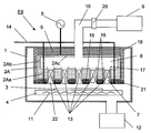
- FIG. 1 is a schematic sub-sectional view of an example of the plasma processing apparatus of the present invention.
- FIG. 2 is a schematic secondary sectional view of another example of the plasma processing apparatus of the present invention.
- FIG. 3 is an enlarged secondary sectional view of a part of the plasma generation electrode of the plasma processing apparatus shown in FIG.
- FIG. 4 is a schematic secondary sectional view of still another example of the plasma processing apparatus of the present invention.
- FIG. 5 is an enlarged secondary sectional view of a part of the plasma generation electrode of the plasma processing apparatus shown in FIG.
- FIG. 6 is a schematic secondary sectional view of still another example of the plasma processing apparatus of the present invention.
- FIG. 7 is an enlarged secondary sectional view of a part of the plasma generation electrode of the plasma processing apparatus shown in FIG. FIG.
- FIG. 8 is a schematic secondary sectional view of still another example of the plasma processing apparatus of the present invention.
- FIG. 9 is an enlarged secondary sectional view of a part of the plasma generation electrode of the plasma processing apparatus shown in FIG.
- FIG. 10 is a schematic secondary sectional view of still another example of the plasma processing apparatus of the present invention.
- FIG. 11 is an enlarged secondary sectional view of a part of the plasma generation electrode of the plasma processing apparatus shown in FIG.
- FIG. 12 is a schematic secondary sectional view of still another example of the plasma processing apparatus of the present invention.
- FIG. 13 is a schematic sub-sectional view of a conventional general plasma CVD apparatus.
- FIG. 14 is a schematic sub-sectional view of the plasma CVD apparatus used in the comparative example.
- FIG. 1 is a schematic sub-sectional view of an example of the plasma processing apparatus of the present invention.
- the plasma processing apparatus E ⁇ b> 1 of the present invention has a vacuum vessel 1. Inside the vacuum vessel 1, a plasma generation electrode 2 for generating plasma is provided.
- the plasma generation electrode 2 in the plasma processing apparatus E1 is formed from an electrode plate 2a.
- a substrate holding mechanism 4 for holding the substrate 3 is provided so that the substrate 3 is positioned at a distance from the lower surface of the electrode plate 2a.
- the size (width) of the surface of the electrode plate 2a facing the substrate 3 is selected in consideration of the size of the substrate 3 attached to the substrate holding mechanism 4 and on which the thin film is formed.
- the plasma generating electrode 2 (electrode plate 2 a) is electrically insulated from the vacuum vessel 1 by an insulator 5 and fixed to the vacuum vessel 1.
- the plasma generating electrode 2 is connected to a power source 6 outside the vacuum vessel 1.
- plasma 7 is generated in the vacuum chamber 1.
- a gas exhaust chamber 8 is formed in the internal space of the vacuum vessel 1 above the upper surface in the drawing of the electrode plate 2a.
- an exhaust pipe 10 having one end opened in the gas exhaust chamber 8 and the other end coupled to the gas exhaust device 9 is provided in the vacuum vessel 1.
- the substrate holding mechanism 4 may be provided with a substrate heating mechanism 11 such as a heater.
- An auxiliary gas exhaust device 12 other than the gas exhaust device 9 may be connected to the vacuum vessel 1.
- an arbitrary power source such as a high frequency power source, a pulse power source, or a DC power source can be used.
- the frequency in the case of using a high frequency power supply can also be set arbitrarily.
- a high-frequency power source in the VHF band is suitable as a high-frequency power source to be used because low-electron temperature and high-density plasma is easily generated. Pulse modulation or amplitude modulation may be applied to the output of the high frequency power source.
- the electrode plate 2a of the plasma generating electrode 2 has a plurality of holes penetrating from the surface facing the substrate 3 (the lower surface of the electrode plate 2a in the drawing) to the gas exhaust chamber 8 side surface (the upper surface of the electrode plate 2a in the drawing). Gas exhaust holes 13 are formed. The plurality of gas exhaust holes 13 are arranged on the surface of the electrode plate 2a facing the substrate 3 (the lower surface of the electrode plate 2a in the drawing) at intervals, that is, at a predetermined pitch.
- a plurality of gas exhaust holes 13 penetrating the electrode plate 2a are formed in the gas exhaust holes 13 after the plasma 7 has entered the gas exhaust holes 13, or have been introduced into the gas exhaust holes 13. Unnecessary substances such as secondary silane and particles are provided to be removed by flowing toward the gas exhaust chamber 8 by the flow of gas exhaust formed in the gas exhaust holes 13.
- each gas exhaust hole 13 is preferably large enough to allow the plasma 7 to enter it.
- the size of the opening of the gas exhaust hole 13 on the surface of the plasma generation electrode 2 facing the substrate 3 of the electrode plate 2a is opposed to the substrate 3 of the electrode plate 2a. It is only necessary to include a virtual circle having a radius of the Debye length of the plasma 7 generated on the front surface of the surface (the lower surface of the electrode plate 2a in the figure).
- an arbitrary shape such as a polygon such as a triangle or a quadrangle, a circle, an ellipse, or a star shape can be selected.
- the stability of the plasma and the maintenance of the inner wall surface of the gas exhaust hole 13 can be selected. From the standpoint of cost when manufacturing the electrode, a circular shape is preferable.
- the cross-sectional shape in the depth direction of the gas exhaust hole 13, that is, the secondary cross-sectional shape of the gas exhaust hole 13 is from the surface (the lower surface of the electrode plate 2a in the figure) facing the substrate 3 of the electrode plate 2a of the plasma generating electrode 2.
- the gas exhaust chamber 8 may have the same shape, or may have a similar shape in the depth direction and a change in size.
- the diameter of the gas exhaust hole 13 is set to the gas exhaust for the purpose of preventing the plasma 7 entering the gas exhaust hole 13 from entering the gas exhaust chamber 8.
- the diameter of the gas exhaust hole 13 is reduced continuously as it approaches the chamber 8 side, or the diameter of the gas exhaust hole 13 from a certain point in the depth direction of the gas exhaust hole 13 to the gas exhaust chamber 8 side is reduced. In the period up to 8, it is preferable to make it smaller in steps.
- the arrangement of the plurality of gas exhaust holes 13 in the electrode plate 2a of the plasma generation electrode 2 can be arbitrarily set.
- the plurality of gas exhaust holes 13 are formed in an equidistant square lattice shape or equidistant regularity. It is preferable that they are arranged in a triangular lattice shape.
- the raw material gas is introduced from the gas introduction pipe 14 to the gas supply pipe 15 located in the vacuum vessel 1.
- the structure of the gas supply pipe 15 and the gas supply port 16 which is the gas discharge end of the gas supply pipe 15 is different from the shower electrode used in a normal CVD apparatus or the like. That is, the gas supply pipe 15 and the gas supply port 16 are arranged so that the gas is supplied toward the inside of the plurality of gas exhaust holes 13.
- the extension line 17 in the flow direction of the gas discharged from the gas supply port 16 intersects the end face opening region 19 (see FIG. 3) at the boundary surface between the gas exhaust hole 13 and the gas exhaust chamber 8.
- a supply pipe 15 and a gas supply port 16 are arranged.
- extension line 17 in the gas flow direction has the direction of the last straight portion including the gas supply port 16 of the gas flow path in the gas supply pipe 15 and passes through the center of the opening of the gas supply port 16.
- end surface opening region 19 refers to a planar closed region formed by an intersection line between the inner wall surface of the gas exhaust hole 13 and the boundary surface between the gas exhaust chamber 8.
- the gas discharged from the gas supply ports 16 removes unnecessary substances such as higher silane and particles in the gas exhaust holes 13. A state where the gas is efficiently blown into the gas exhaust chamber 8 is formed.
- the extension line 17 in the flow direction of the gas discharged from the gas supply port 16 does not intersect the end face opening region 19 and collides with the wall surface of the gas exhaust hole 13, the flow of the discharged gas is The collision with the wall surface is disturbed and messy, and as a result, backflow of unnecessary substances in the direction of the substrate 3 may occur.
- the gas exhaust chamber 8 is formed, for example, as a region (space) surrounded by a part of the inner wall surface of the vacuum vessel 1 and the upper surface of the electrode plate 2a of the plasma generating electrode 2 as shown in FIG. If the wall surface forming the gas exhaust chamber 8 has the same potential, the occurrence of abnormal discharge in the gas exhaust chamber 8 is suppressed. Therefore, the gas exhaust chamber 8 is preferably formed inside the plasma generation electrode 2, that is, by a region (space) surrounded by the plasma generation electrode 2.
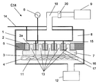
- FIG. 2 shows a schematic cross-sectional view of an example of a plasma processing apparatus in which the gas exhaust chamber 8 is formed inside the plasma generation electrode 2.
- the plasma processing apparatus E2 shown in FIG. 2 has a plasma generation electrode 2A in the vacuum vessel 1.
- the structure of the plasma generation electrode 2A is different from the structure of the plasma generation electrode 2 in FIG. That is, the plasma generating electrode 2A is a type having the gas exhaust chamber 8 therein.
- the plasma generating electrode 2A extends from the electrode plate 2Aa, the periphery thereof, the side wall 2Ab formed from the electrode base, and the side wall 2Ab that is coupled to the side wall 2Ab so as to close the space surrounded by the side wall 2Ab.
- the top plate 2Ac is formed from.
- the plasma generating electrode 2A is composed of a housing formed of an electrode base material, and has a gas exhaust chamber 8 therein.
- the plasma generation electrode 2A is fixed to the vacuum vessel 1 through an insulator 5.
- An earth shield 18 is disposed on the side surface of the plasma generation electrode 2A via a space gap of several millimeters. The earth shield 18 prevents unnecessary discharge generation on the side surface of the plasma generation electrode 2A. Since the wall surface of the gas exhaust chamber 8 is formed by the plasma generation electrode 2A, the entire wall surface of the gas exhaust chamber 8 has the same potential, and the generation of an electric field inside the gas exhaust chamber 8 is prevented. As a result, the gas exhaust chamber The occurrence of abnormal discharge inside 8 is prevented.
- the electrode plate 2Aa in the plasma generation electrode 2A has the same structure as the electrode plate 2a in FIG.
- Other constituent elements in the plasma processing apparatus E2 of FIG. 2 are the same as or substantially the same as the constituent elements of the plasma processing apparatus E1 of FIG. Is used. The same applies to other drawings.
- FIG. 3 is an enlarged secondary sectional view of a part of the plasma generating electrode 2A in FIG.
- FIG. 3 shows an example of the configuration of the gas supply port 16.
- one example of the end face opening region 19 is indicated by a dotted line.
- a gas supply port 16 is provided on the inner wall surface of the gas exhaust hole 13, and an extended line 17 in the flow direction of the gas discharged from the gas supply port 16 is a boundary surface of the gas exhaust chamber 8 of the gas exhaust hole 13.
- the direction of the gas supply pipe 15 is set so as to intersect the end face opening region 19 in FIG.
- FIG. 4 shows a secondary sectional view of another example of the plasma processing apparatus.
- FIG. 5 shows an enlarged cross-sectional view of a part of the plasma generation electrode in the plasma processing apparatus E4 of FIG. 4 and 5
- the gas exhaust hole 13 in the plasma processing apparatus E4 is an example in which the inner diameter changes in the longitudinal direction (depth direction) of the gas exhaust hole 13.
- FIG. 5 shows a gas exhaust hole 13 in which the inner diameter on the inlet side is larger than the inner diameter on the outlet side (gas exhaust chamber 8 side), and the inner diameter changes in two stages.
- the gas supply pipe is arranged such that the extension line 17 in the flow direction of the gas discharged from the gas supply port 16 intersects the end face opening region 19 at the boundary surface between the gas exhaust hole 13 and the gas exhaust chamber 8. 15 directions are set.
- FIG. 6 shows a sectional view of still another example of the plasma processing apparatus.
- FIG. 7 shows an enlarged secondary sectional view of a part of the plasma generation electrode in the plasma processing apparatus E6 of FIG. 6 and 7, the gas supply pipe 15 in the plasma processing apparatus E ⁇ b> 6 is provided in a state of passing through the inside of the gas exhaust hole 13.
- a gas supply port 16 is provided on the tube wall of the gas supply tube 15 that passes through the gas exhaust hole 13. Gas is blown into the gas exhaust hole 13 from the gas supply port 16 so as to reach the gas exhaust chamber 8 through the gas exhaust hole 13.
- the last straight portion including the gas supply port 16 of the gas flow path in the gas supply pipe 15” in the extension line 17 in the gas flow direction is formed on the tube wall of the gas supply pipe 15. This refers to a straight portion in the thickness direction of the tube wall of the formed through hole.
- the depth (length in the longitudinal direction) of the gas exhaust hole 13 is defined as a depth (length) d.
- the range of the depth d of the gas exhaust hole 13 is not particularly limited. However, if it is too shallow, unnecessary substances sent into the gas exhaust chamber 8 may flow backward in the direction of the substrate 3, and in order to prevent the plasma 7 from entering the gas exhaust chamber 8, it is better to be deep to some extent. On the other hand, if it is too deep, the exhaust conductance by the gas exhaust hole 13 becomes small, and the exhaust capability may be reduced. Therefore, the depth d of the gas exhaust hole 13 is preferably 10 mm to 60 mm, and more preferably 20 mm to 40 mm.
- the position of the gas supply port 16 in the depth direction of the gas exhaust hole 13 can be appropriately selected.
- the gas supply port 16 may be provided as close to the substrate 3 side in the gas exhaust hole 13 as possible.
- the position is preferably within 10 mm from the substrate 3 side and more preferably within 5 mm in the depth direction of the gas exhaust hole 13 as viewed from the substrate 3 side surface of the plasma generating electrodes 2 and 2A.
- the gas exhaust chamber 8 is formed in a space that is sufficiently larger than the gas exhaust hole 13 from the viewpoint of preventing unnecessary substances sent into the gas exhaust chamber 8 from flowing back to the substrate 3 side. It is desirable that The height H of the gas exhaust chamber 8 when viewed in the depth direction of the gas exhaust hole 13 is preferably 20 mm or more and the depth d of the gas exhaust hole 13 or more. Further, it is preferable that the inner diameter of the exhaust pipe 10 connecting the gas exhaust chamber 8 and the gas exhaust device 9 is as large as possible from the viewpoint of securing the exhaust capacity. A plurality of exhaust pipes 10 may be provided in parallel. In order to adjust the pressure in the vacuum vessel 1, a pressure adjustment valve 20 is preferably provided in the middle of the exhaust pipe 10.
- FIG. 8 is a schematic sub-sectional view of still another example of the plasma processing apparatus of the present invention.
- the plasma generating electrode 2A is fixed to the vacuum vessel 1 with an insulator 5 interposed therebetween.
- An earth shield 18 is disposed on the side surface of the plasma generation electrode 2A via a space gap of several millimeters. The earth shield 18 prevents unnecessary discharge generation on the side surface of the plasma generation electrode 2A.
- a plasma confining electrode 21 is provided on the surface of the electrode plate 2Aa of the plasma generating electrode 2A that faces the substrate 3.
- the plasma confinement electrode 21 has through holes 22 at positions facing the plurality of gas exhaust holes 13 of the electrode plate 2Aa of the plasma generation electrode 2A.
- the plasma generation location is limited to the inside of the gas exhaust hole 13, and the plasma generated in the space between the plasma confinement electrode 21 and the substrate 3 can be weakened, or the plasma confinement Plasma can be prevented from being generated in the space between the electrode 21 and the substrate 3. Thereby, the chance that the unnecessary substance produced
- the plasma confinement electrode 21 is disposed substantially parallel to the electrode plate 2Aa of the plasma generation electrode 2A with a space therebetween. If the distance between the electrode plate 2Aa of the plasma generation electrode 2A and the plasma confinement electrode 21 is too narrow, there is a risk of short circuit or abnormal discharge due to a film attached to the electrode. If it is too wide, unnecessary plasma may be generated in the space between the electrode plate 2Aa of the plasma generation electrode 2A and the plasma confinement electrode 21. Therefore, the distance between the electrode plate 2Aa of the plasma generating electrode 2A and the plasma confinement electrode 21 is preferably 0.3 mm to 5 mm, more preferably 0.5 mm to 3 mm, and 0.8 mm to 1.5 mm. It is more preferable that
- the potential of the plasma confinement electrode 21 can be arbitrarily selected according to the situation. However, it is preferable that the plasma confinement electrode 21 is set to the ground potential from the viewpoint that the structure of the electrode is simple and the plasma is confined stably. For example, there is a method of connecting and fixing the plasma confinement electrode 21 to the earth shield 18 or a method of connecting and fixing the plasma confinement electrode 21 to the wall surface of the vacuum vessel 1. Further, the plasma confinement electrode 21 is electrically insulated from the earth shield 18 and the vacuum vessel 1 and fixed, and a power source (not shown) is connected to the plasma confinement electrode 21 so that an arbitrary potential is applied to the plasma confinement electrode 21. It is also possible to control the confinement state.
- FIG. 9 is an enlarged cross-sectional view of a part of the electrode plate 2Aa and the plasma confinement electrode 21 of the plasma generation electrode 2A in FIG.
- the gas supply port 16 is provided on the inner wall surface of the through hole 22 of the plasma confinement electrode 21, and gas is supplied from the plasma confinement electrode 21, whereby the gas exhaust hole 13 of the electrode plate 2 ⁇ / b> Aa of the plasma generation electrode 2 ⁇ / b> A is supplied.
- the gas supply port 16 is provided on the inner wall surface, a stronger gas flow can be generated from the substrate 3 side with respect to the plasma. This configuration is preferable from the viewpoint of unnecessary substance discharge efficiency.
- FIG. 10 shows a secondary sectional view of still another plasma processing apparatus.
- the plasma processing apparatus E ⁇ b> 10 of FIG. 10 is another aspect in the case of supplying gas from the plasma confinement electrode 21.
- FIG. 11 is an enlarged secondary sectional view of a part of the electrode plate 2Aa of the plasma generation electrode 2A and the plasma confinement electrode 21 in FIG.
- the gas supply pipe 15 is provided inside the through hole 22 of the plasma confinement electrode 21, and the gas supply port 16 is provided on the tube wall of the gas supply pipe 15.
- An extension line 17 in the gas flow direction is set so as to pass through the through hole 22 and toward the gas exhaust hole 13.
- the degree of freedom in adjusting the gas flow direction is increased. Further, the fine processing of the shape of the gas supply port 16 becomes possible, and the shape of the gas supply port 16 having more effective gas blowing characteristics can be selected.
- FIG. 12 is a schematic sub-sectional view of still another example of the plasma processing apparatus of the present invention.
- the plasma confinement electrode 21 is provided with a plasma confinement electrode heating mechanism 24.
- any heating means such as a resistance heater, a heat medium flow tube, and an infrared lamp can be used. From the viewpoint of ease of electrode assembly and temperature controllability, a resistance heater is used. Is preferred.
- the heating temperature is preferably about 100 ° C. to about 350 ° C., although the optimum value varies depending on the process to be performed.
- a gas buffer space 25 is provided inside the plasma confinement electrode 21.
- the gas buffer space 25 is disposed in the middle of the gas supply pipe 15 provided inside the plasma confinement electrode 21 and is a space in which the flowing gas can be temporarily retained.
- the plasma processing apparatus is used as an apparatus for performing various plasma processes such as film formation, etching, and surface treatment. In particular, it exerts its power in a process in which unnecessary by-products are formed during processing. For example, in dry etching using halogen gas, there is a generation of particles due to film peeling during processing or deterioration of internal structures, which adversely affects the process. Therefore, the plasma processing apparatus according to the present invention is used as a means for removing the particles. I can do it.
- the plasma processing apparatus according to the present invention can be suitably used as a plasma CVD apparatus.
- the plasma CVD apparatus comprising the plasma processing apparatus of the present invention prevents the high-order silane and particles generated in the process of forming the amorphous silicon thin film on the substrate as much as possible and reduces the film quality due to the mixing into these thin films. In particular, it functions effectively to produce an amorphous silicon thin film having a good film quality.
- the first embodiment for forming an amorphous silicon thin film is a method for producing an amorphous silicon thin film using the plasma processing apparatus E4 shown in FIG.
- the cross-sectional shape of the gas exhaust hole 13 formed in the electrode plate 2Aa of the plasma generating electrode 2A is a circle, and the depth d is 20 mm.
- the electrode plate 2Aa is formed of a regular square electrode plate having a side length of 185 mm.
- gas exhaust holes 13 are arranged in a 17 mm pitch square lattice. As shown in FIG. 5, the diameter of the gas exhaust hole 13 is smaller on the gas exhaust chamber 8 side.
- the depth d1 of the gas exhaust hole 13 is 15 mm, the diameter D1 on the inlet side of the gas exhaust hole 13 is 10 mm, and the diameter D2 on the outlet side of the gas exhaust hole 13 is 6 mm.
- the gas supply port 16 is provided at a position where the depth d2 from the surface of the electrode plate 2Aa on the substrate 3 side is 3 mm, and the inner diameter of the gas supply pipe 15 reaching the gas supply port 16 is 0.5 mm.
- the length direction of the gas supply pipe 15 is inclined so that the angle ⁇ with respect to the normal direction of the main plane formed by the electrode plate 2Aa is 20 degrees.
- Four gas supply ports 16 are provided at equal intervals in the circumferential direction of each gas exhaust hole 13.
- the gas supply port 16 is arranged so that the extension line 17 in the flow direction of the gas discharged from the gas supply port 16 intersects the end surface opening region 19 in the boundary surface between the gas exhaust hole 13 and the gas exhaust chamber 8. Yes.
- the height H of the gas exhaust chamber 8 (the distance between the electrode plate 2Aa and the top plate 2Ac) is 35 mm.
- An amorphous silicon thin film is formed on a glass substrate using such a plasma processing apparatus E4.
- a glass substrate 3 is set on the substrate holding mechanism 4 of the plasma processing apparatus E 4, and the substrate 3 is heated by the substrate heating mechanism 11.
- the gas in the vacuum vessel 1 is sufficiently evacuated by the auxiliary gas exhaust device 12, that is, after the pressure in the vacuum vessel 1 is reduced to a level that enables a desired plasma treatment, the gas is exhausted from the exhaust action by the auxiliary gas exhaust device 12. Switch to exhaust action by device 9.
- Silane gas is introduced from the gas introduction pipe 14 as a raw material gas, and the pressure in the vacuum vessel 1 is adjusted by the pressure adjustment valve 20. Power is supplied from the power source 6 to the plasma generating electrode 2 ⁇ / b> A, plasma is generated in the vacuum vessel 1 to decompose the source gas, and an amorphous silicon thin film is formed on the substrate 3.
- the amorphous silicon thin film formed on the substrate 3 in this way has a very low defect density in the film and good electrical characteristics.
- this amorphous silicon thin film is applied to a power generation layer of a solar cell, it is possible to obtain a solar cell with little photodegradation of the film and high photoelectric conversion efficiency.
- the source gas in this case may be a gas containing at least silane gas, and may be 100% silane gas or silane gas diluted with a rare gas such as hydrogen or argon.
- the second embodiment for forming an amorphous silicon thin film is a method for producing an amorphous silicon thin film using the plasma processing apparatus E6 shown in FIG.
- the cross-sectional shape of the gas exhaust hole 13 formed in the electrode plate 2Aa of the plasma generation electrode 2A is a circle.
- the diameter D1 of the gas exhaust hole 13 is 10 mm, and the depth d is 30 mm.
- the electrode plate 2Aa is formed of a regular square electrode plate having a side length of 185 mm.
- a gas supply pipe 15 is provided in the direction perpendicular to the central axis of the gas exhaust hole 13 (that is, the horizontal direction in the figure) through the gas exhaust hole 13.
- the gas supply pipe 15 has an outer diameter of 3 mm and an inner diameter of 1.5 mm.
- the gas supply port 16 is formed by a hole provided in the tube wall of the gas supply pipe 15 in the vicinity of the central axis of the gas exhaust hole 13. The diameter of the gas supply port 16 is 0.5 mm.
- the gas supply port 16 is arranged so that the extension line 17 in the flow direction of the gas discharged from the gas supply port 16 intersects the end surface opening region 19 in the boundary surface between the gas exhaust hole 13 and the gas exhaust chamber 8. Yes. Thereby, the gas discharged from the gas supply port 16 reaches the gas exhaust chamber 8 without colliding with the wall surface of the gas exhaust hole 13.
- the height H of the gas exhaust chamber 8 (the distance between the electrode plate 2Aa and the top plate 2Ac) is 30 mm.
- an amorphous silicon thin film is formed on a glass substrate.
- a glass substrate 3 is set on the substrate holding mechanism 4 of the plasma processing apparatus E 6, and the substrate 3 is heated by the substrate heating mechanism 11.
- silane gas is introduced from the gas introduction pipe 14 as a raw material gas.
- the pressure in the vacuum vessel 1 is adjusted by the pressure adjustment valve 20. Power is supplied from the power source 6 to the plasma generating electrode 2 ⁇ / b> A, plasma is generated in the vacuum vessel 1 to decompose the source gas, and an amorphous silicon thin film is formed on the substrate 3.
- the amorphous silicon thin film thus formed on the substrate 3 also has a very low defect density in the film, as in the first embodiment.
- a third embodiment of forming an amorphous silicon thin film is a method for manufacturing an amorphous silicon thin film using the plasma processing apparatus E8 shown in FIG.
- the cross-sectional shape of the gas exhaust hole 13 formed in the electrode plate 2Aa of the plasma generation electrode 2A is a circle.
- the diameter D1 of the gas exhaust hole 13 is 10 mm, and the depth d is 30 mm.
- the electrode plate 2Aa is formed of an electrode made of a regular square having a side length of 185 mm.
- a plasma confinement electrode 21 is provided on the surface of the electrode plate 2Aa facing the substrate 3.
- the plasma confinement electrode 21 is provided with a through hole 22 at a position facing the plurality of gas exhaust holes 13 of the electrode plate 2Aa.
- the diameter of the through hole 22 is 10 mm.
- the thickness of the plasma confinement electrode 21 is 15 mm.
- the distance between the plasma confinement electrode 21 and the electrode plate 2Aa is 1 mm.
- the plasma confinement electrode 21 is fixed to the earth shield 18 so as to be electrically connected to a ground potential.
- a part of the gas supply pipe 15 extending from the gas introduction pipe 14 is embedded in the plasma confinement electrode 21.
- the tip of the gas supply pipe 15 embedded in the plasma confinement electrode 21 is opened on the inner wall surface of the through hole 22 to form a gas supply port 16.
- An extension line 17 in the flow direction of the gas discharged from the gas supply port 16 passes through the through hole 22 of the plasma confinement electrode 21 and the gas exhaust hole 13 of the electrode plate 2Aa, and the gas exhaust chamber of the gas exhaust hole 13
- a gas supply port 16 is arranged so as to cross the end face opening region 19 on the boundary surface with the gas and to reach the gas exhaust chamber 8.
- the height H of the gas exhaust chamber 8 (the distance between the electrode plate 2Aa and the top plate 2Ac) is 30 mm.
- An amorphous silicon thin film is formed on a glass substrate using such a plasma processing apparatus E8.
- the glass substrate 3 is set on the substrate holding mechanism 4 of the plasma processing apparatus E8, and the substrate 3 is heated by the substrate heating mechanism 11.
- silane gas is introduced from the gas introduction pipe 14 as a raw material gas.
- the pressure in the vacuum vessel 1 is adjusted by the pressure adjustment valve 20. Power is supplied from the power source 6 to the plasma generating electrode 2 ⁇ / b> A, plasma is generated in the vacuum vessel 1 to decompose the source gas, and an amorphous silicon thin film is formed on the substrate 3.
- the amorphous silicon thin film thus formed on the substrate 3 further exceeds the results of the first embodiment and the second embodiment, and the defect density in the film is very low.
- the fourth embodiment for forming an amorphous silicon thin film is a method for producing an amorphous silicon thin film using the plasma processing apparatus E10 shown in FIG.
- the cross-sectional shape of the gas exhaust hole 13 even formed in the electrode plate 2Aa of the plasma generating electrode 2A is circular.
- the diameter D1 of the gas exhaust hole 13 is 10 mm, and the depth d is 30 mm.
- the electrode plate 2Aa is formed of a regular square electrode plate having a side length of 185 mm.
- a plasma confinement electrode 21 is provided on the surface of the electrode plate 2Aa facing the substrate 3.
- the plasma confinement electrode 21 is provided with a through hole 22 at a position facing the plurality of gas exhaust holes 13 of the electrode plate 2Aa.
- the diameter of the through hole 22 is 10 mm.
- the thickness of the plasma confinement electrode 21 is 15 mm.
- the distance between the plasma confinement electrode 21 and the electrode plate 2Aa is 1 mm.
- the plasma confinement electrode 22 is fixed to the earth shield 18 so as to be electrically connected to a ground potential.
- a part of the gas supply pipe 15 extending from the gas introduction pipe 14 is embedded in the plasma confinement electrode 21.
- the gas supply pipe 15 embedded in the plasma confinement electrode 21 further extends, passes through the through hole 22, and passes through the plasma confinement electrode 21 again.
- the gas supply pipe 15 has an outer diameter of 3 mm and an inner diameter of 1.5 mm.
- the portion that passes through the through hole 22 of the gas supply pipe 15 is provided in a direction perpendicular to the central axis of the gas exhaust hole 13 (that is, in the horizontal direction in the figure).
- the gas supply port 16 is formed by a hole provided in the tube wall of the gas supply pipe 15 in the vicinity of the central axis of the gas exhaust hole 13.
- the diameter of the gas supply port 16 is 0.5 mm.
- An extension line 17 in the flow direction of the gas discharged from the gas supply port 16 passes through the through hole 22 of the plasma confinement electrode 21 and the gas exhaust hole 13 of the electrode plate 2Aa, and the gas exhaust chamber of the gas exhaust hole 13
- a gas supply port 16 is arranged so as to cross the end face opening region 19 on the boundary surface with the gas and to reach the gas exhaust chamber 8.
- the height H of the gas exhaust chamber 8 (the distance between the electrode plate 2Aa and the top plate 2Ac) is 30 mm.
- an amorphous silicon thin film is formed on a glass substrate.
- the glass substrate 3 is set on the substrate holding mechanism 4 of the plasma processing apparatus E10, and the substrate 3 is heated by the substrate heating mechanism 11.
- silane gas is introduced from the gas introduction pipe 14 as a raw material gas.
- the pressure in the vacuum vessel 1 is adjusted by the pressure adjustment valve 20. Power is supplied from the power source 6 to the plasma generating electrode 2 ⁇ / b> A, plasma is generated in the vacuum vessel 1 to decompose the source gas, and an amorphous silicon thin film is formed on the substrate 3.
- the amorphous silicon thin film formed in this way has a very low defect density in the film as in the third embodiment.
- the amorphous silicon thin film is formed on the substrate based on the above-described first embodiment of forming the amorphous silicon thin film, and Si—H 2 in the thin film thus obtained is formed.
- the binding concentration was determined, and the quality of the obtained thin film was evaluated based on it.
- the substrate 3 was set on the substrate holding mechanism 4, and the substrate 3 was heated to 220 ° C. by the substrate heating mechanism 11.
- the auxiliary gas exhaust device 12 After the gas in the vacuum vessel 1 is exhausted by the auxiliary gas exhaust device 12 until the pressure in the vacuum vessel 1 becomes 1 ⁇ 10 ⁇ 4 Pa or less, the exhaust action of the gas in the vacuum vessel 1 is The device 12 was switched to the gas exhaust device 9.
- a silane gas of 300 sccm as a source gas was introduced from the gas introduction pipe 14 to the gas supply port 16 through the gas supply pipe 15, and the pressure in the vacuum vessel 1 was adjusted to 30 Pa by the pressure adjustment valve 20.
- a high frequency power source having a frequency of 60 MHz was used as the power source 6, and 50 W of power was supplied to the plasma generation electrode 2 ⁇ / b> A to generate plasma, and an amorphous silicon thin film was formed on the substrate 3.
- the Si—H 2 bond concentration in the obtained amorphous silicon thin film was determined by FT-IR measurement.
- FT-IR measurement FT-720 manufactured by HORIBA was used. The resolution in this measurement was 4 cm ⁇ 1 and the number of integrations was 16 times.
- the Si—H 2 bond concentration was determined by the following procedure.
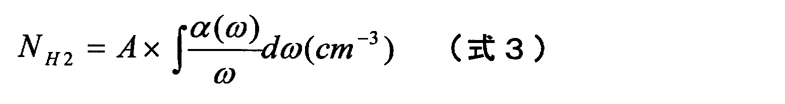
- Equation 1 A peak at 2090 cm ⁇ 1 was separated from a peak near 2000 cm ⁇ 1 using the Gaussian function shown in Equation 1.
- Equation 1 h is the peak height, ⁇ is the peak width, and ⁇ p is the peak wave number.
- Ts represents the transmittance (%) of single crystal silicon
- ⁇ T represents the transmittance (%) of the amorphous silicon thin film obtained by subtracting the baseline
- d represents the film thickness (cm)
- ⁇ represents Wave number (cm ⁇ 1 )
- A represents a proportionality constant of 1.4 ⁇ 10 20 cm ⁇ 2 .
- the Si—H 2 bond concentration of the obtained amorphous silicon thin film was 0.7%, and it was confirmed that the obtained amorphous silicon thin film was a film having a low defect density in the film.
- an amorphous silicon thin film was formed on the substrate by the same procedure as in Example 1 based on the second embodiment for forming an amorphous silicon thin film.
- the Si—H 2 bond concentration in the film was calculated based on the same method as in Example 1.
- the Si—H 2 bond concentration of the obtained amorphous silicon thin film was 0.6%, and it was confirmed that the amorphous silicon thin film has a low defect density in the film.
- Example 1 Using the plasma processing apparatus E8 shown in FIGS. 8 and 9, the same as Example 1 except that 80 W of power is supplied to the plasma generating electrode 2A based on the third embodiment for forming the amorphous silicon thin film. According to the procedure, an amorphous silicon thin film was formed on the substrate. With respect to the obtained amorphous silicon thin film, the Si—H 2 bond concentration in the film was calculated based on the same method as in Example 1. As a result, the Si—H 2 bond concentration of the obtained amorphous silicon thin film was 0.3%, and it was confirmed that the obtained amorphous silicon thin film was a film having a low defect density in the film.
- Example 1 Using the plasma processing apparatus E10 shown in FIGS. 10 and 11, the same as Example 1 except that 80 W of electric power was supplied to the plasma generating electrode 2A based on the above-described fourth embodiment of forming an amorphous silicon thin film. According to the procedure, an amorphous silicon thin film was formed on the substrate. With respect to the obtained amorphous silicon thin film, the Si—H 2 bond concentration in the film was calculated based on the same method as in Example 1. As a result, the Si—H 2 bond concentration of the obtained amorphous silicon thin film was 0.1%, and it was confirmed that the obtained amorphous silicon thin film had a sufficiently low defect density in the film.
- An amorphous silicon thin film was formed on the substrate P3 using a conventional general parallel plate type plasma CVD apparatus PA13 shown in FIG.
- a silane gas of 50 sccm as a source gas was introduced into the vacuum vessel P1 from the showerhead-like gas supply port P16 provided in the plasma generation electrode P2 via the gas introduction pipe P14.
- the pressure in the vacuum vessel P1 was adjusted to 30 Pa by the pressure adjustment valve P20.
- a high frequency power source having a frequency of 13.56 MHz was used as the power source P6, and plasma was generated by supplying power of 30 W to the plasma generating electrode P2, thereby forming an amorphous silicon thin film on the substrate P3.
- the Si—H 2 bond concentration in the film was calculated based on the same method as in Example 1.
- the Si—H 2 bond concentration of the obtained amorphous silicon thin film was 1.5%, and the amorphous silicon thin film was confirmed to be a film having a high defect concentration in the film.
- An amorphous silicon thin film was formed using a plasma CVD apparatus C14 shown in FIG.
- the plasma CVD apparatus C14 is provided with a plurality of exhaust holes 12 in the discharge electrode 2 with respect to the plasma processing apparatus E1 shown in FIG. 1, the gas supply port has a conventional showerhead-like arrangement, and the gas flow In the plasma CVD apparatus, the direction extension line 17 is in the direction of the substrate 3.
- a silane gas of 150 sccm as a source gas was introduced into the vacuum vessel 1 through a gas introduction pipe 14 from a showerhead-like gas supply port 16 provided in the plasma generation electrode 2.
- An amorphous silicon thin film was formed on the substrate 2 by the same procedure as in Example 1 except that 50 W of electric power was supplied to the plasma generating electrode 2 to generate plasma.
- the Si—H 2 bond concentration in the film was calculated based on the same method as in Example 1.
- the Si—H 2 bond concentration of the obtained amorphous silicon thin film was 1.0%, and it was confirmed that the obtained amorphous silicon thin film was a film whose defect concentration in the film was not sufficiently low. It was done.
- the plasma processing apparatus according to the present invention is preferably used for forming a thin film having good film quality.
- the plasma processing apparatus according to the present invention is also used as an etching apparatus or a plasma surface modification apparatus.
Abstract
Description
(b)該真空容器の内部に設けられたプラズマ生成電極、
(c)前記真空容器の内部において、前記プラズマ生成電極に対向して間隔をおいて位置せしめられる基板を保持するための基板保持機構、
(d)前記真空容器の内部を減圧に保持するため、前記真空容器の内部において、前記プラズマ生成電極と前記真空容器の内壁面との間に形成されたガス排気室に開口して前記真空容器に接続されたガス排気装置、
(e)前記プラズマ生成電極に接続され、該プラズマ生成電極に電力を供給する電源、および、
(f)プラズマ処理用の原料ガスを前記真空容器の内部に導入するために、前記真空容器に接続されたガス導入管を備えたプラズマ処理装置において、
(g)前記プラズマ生成電極が、前記基板保持機構に基板が保持されたときに、該基板に対向する面から該プラズマ生成電極を貫通し前記ガス排気室へ至る複数のガス排気孔を有し、
(h)前記ガス導入管に接続して設けられたガス供給管が、前記複数のガス排気孔の内部に向けて前記原料ガスを吐出するためのガス供給口を有し、
(i)前記ガス供給管および前記ガス供給口が、該ガス供給口から吐出される前記原料ガスの流れ方向の延長線が前記ガス排気孔の前記ガス排気室との境界面における端面開口領域と交差するように配置されているプラズマ処理装置。 (A) a vacuum vessel,
(B) a plasma generating electrode provided inside the vacuum vessel;
(C) a substrate holding mechanism for holding a substrate positioned at an interval facing the plasma generation electrode in the vacuum vessel;
(D) In order to keep the inside of the vacuum container at a reduced pressure, the vacuum container is opened inside the vacuum container by opening a gas exhaust chamber formed between the plasma generation electrode and the inner wall surface of the vacuum container. Gas exhaust device connected to,
(E) a power source connected to the plasma generating electrode and supplying power to the plasma generating electrode; and
(F) In a plasma processing apparatus provided with a gas introduction pipe connected to the vacuum vessel in order to introduce a source gas for plasma processing into the vacuum vessel,
(G) When the substrate is held by the substrate holding mechanism, the plasma generation electrode has a plurality of gas exhaust holes that penetrate the plasma generation electrode from the surface facing the substrate and reach the gas exhaust chamber. ,
(H) a gas supply pipe connected to the gas introduction pipe has a gas supply port for discharging the source gas toward the inside of the plurality of gas exhaust holes;
(I) In the gas supply pipe and the gas supply port, an extension line in a flow direction of the source gas discharged from the gas supply port is an end surface opening region at a boundary surface between the gas exhaust hole and the gas exhaust chamber. A plasma processing apparatus arranged to intersect.


2、2A: プラズマ生成電極
2a、2Aa: 電極板
2Ab: 電極の側壁
2Ac: 電極の天板
3: 基板
4: 基板保持機構
5: 絶縁物
6: 電源
7: プラズマ
8: ガス排気室
9: ガス排気装置
10: 排気配管
11: 基板加熱機構
12: 補助ガス排気装置
13: ガス排気孔
14: ガス導入管
15: ガス供給管
16: ガス供給口
17: ガスの流れ方向の延長線
18: アースシールド
19: 端面開口領域
20: 圧力調整バルブ
21: プラズマ閉じ込め電極
22: 貫通孔
23: 接地電極
24: プラズマ閉じ込め電極加熱機構
25: ガスバッファ空間
C14: プラズマCVD装置
E1、E2、E4、E6、E8、E10、E12: プラズマ処理装置
P1: 真空容器
P2: プラズマ生成電極
P3: 基板
P6: 電源
P7: プラズマ
P9: ガス排気装置
P10: 排気配管
P11: 基板加熱機構
P14: ガス導入管
P16: ガス供給口
P20: 圧力調整バルブ
PA13: プラズマCVD装置 1:
Claims (10)
- (a)真空容器、
(b)該真空容器の内部に設けられたプラズマ生成電極、
(c)前記真空容器の内部において、前記プラズマ生成電極に対向して間隔をおいて位置せしめられる基板を保持するための基板保持機構、
(d)前記真空容器の内部を減圧に保持するため、前記真空容器の内部において、前記プラズマ生成電極と前記真空容器の内壁面との間に形成されたガス排気室に開口して前記真空容器に接続されたガス排気装置、
(e)前記プラズマ生成電極に接続され、該プラズマ生成電極に電力を供給する電源、および、
(f)プラズマ処理用の原料ガスを前記真空容器の内部に導入するために、前記真空容器に接続されたガス導入管を備えたプラズマ処理装置において、
(g)前記プラズマ生成電極が、前記基板保持機構に基板が保持されたときに、該基板に対向する面から該プラズマ生成電極を貫通し前記ガス排気室へ至る複数のガス排気孔を有し、
(h)前記ガス導入管に接続して設けられたガス供給管が、前記複数のガス排気孔の内部に向けて前記原料ガスを吐出するためのガス供給口を有し、
(i)前記ガス供給管および前記ガス供給口が、該ガス供給口から吐出される前記原料ガスの流れ方向の延長線が前記ガス排気孔の前記ガス排気室との境界面における端面開口領域と交差するように配置されているプラズマ処理装置。 (A) a vacuum vessel,
(B) a plasma generating electrode provided inside the vacuum vessel;
(C) a substrate holding mechanism for holding a substrate positioned at an interval facing the plasma generation electrode in the vacuum vessel;
(D) In order to keep the inside of the vacuum container at a reduced pressure, the vacuum container is opened inside the vacuum container by opening a gas exhaust chamber formed between the plasma generation electrode and the inner wall surface of the vacuum container. Gas exhaust device connected to,
(E) a power source connected to the plasma generating electrode and supplying power to the plasma generating electrode; and
(F) In a plasma processing apparatus provided with a gas introduction pipe connected to the vacuum vessel in order to introduce a source gas for plasma processing into the vacuum vessel,
(G) When the substrate is held by the substrate holding mechanism, the plasma generation electrode has a plurality of gas exhaust holes that penetrate the plasma generation electrode from the surface facing the substrate and reach the gas exhaust chamber. ,
(H) a gas supply pipe connected to the gas introduction pipe has a gas supply port for discharging the source gas toward the inside of the plurality of gas exhaust holes;
(I) In the gas supply pipe and the gas supply port, an extension line in a flow direction of the source gas discharged from the gas supply port is an end surface opening region at a boundary surface between the gas exhaust hole and the gas exhaust chamber. A plasma processing apparatus arranged to intersect. - 前記ガス排気室が、前記プラズマ生成電極の内部に設けられている請求項1に記載のプラズマ処理装置。 The plasma processing apparatus according to claim 1, wherein the gas exhaust chamber is provided inside the plasma generation electrode.
- 前記ガス供給口が、前記ガス排気孔の内壁面に開口している請求項1に記載のプラズマ処理装置。 The plasma processing apparatus according to claim 1, wherein the gas supply port is opened on an inner wall surface of the gas exhaust hole.
- 前記ガス供給管および前記ガス供給口が、前記ガス排気孔の内部に位置している請求項1に記載のプラズマ処理装置。 The plasma processing apparatus according to claim 1, wherein the gas supply pipe and the gas supply port are located inside the gas exhaust hole.
- 前記基板保持機構に基板が保持されたときに、該基板に対向する前記プラズマ生成電極の面に対して、間隔を置いて略平行に設けられたプラズマ閉じ込め電極を備え、該プラズマ閉じ込め電極が、前記プラズマ生成電極の複数のガス排気孔に対応する位置に、貫通孔を有する請求項1に記載のプラズマ処理装置。 When the substrate is held by the substrate holding mechanism, it comprises a plasma confinement electrode provided substantially parallel to the surface of the plasma generation electrode facing the substrate, the plasma confinement electrode, The plasma processing apparatus of Claim 1 which has a through-hole in the position corresponding to the several gas exhaust hole of the said plasma production electrode.
- 前記ガス供給口が、前記プラズマ閉じ込め電極の前記貫通孔の内壁面に開口している請求項5に記載のプラズマ処理装置。 The plasma processing apparatus according to claim 5, wherein the gas supply port opens on an inner wall surface of the through hole of the plasma confinement electrode.
- 前記ガス供給管および前記ガス供給口が、前記プラズマ閉じ込め電極の前記貫通孔の内部に位置している請求項5に記載のプラズマ処理装置。 The plasma processing apparatus according to claim 5, wherein the gas supply pipe and the gas supply port are located inside the through hole of the plasma confinement electrode.
- 前記プラズマ閉じ込め電極が、プラズマ閉じ込め電極加熱機構を有し、前記プラズマ閉じ込め電極の内部に、ガスバッファ空間が設けられている請求項5に記載のプラズマ処理装置。 The plasma processing apparatus according to claim 5, wherein the plasma confinement electrode has a plasma confinement electrode heating mechanism, and a gas buffer space is provided inside the plasma confinement electrode.
- 前記プラズマ処理装置におけるプラズマ処理が、化学的気相蒸着(CVD)である請求項1に記載のプラズマ処理装置。 The plasma processing apparatus according to claim 1, wherein the plasma processing in the plasma processing apparatus is chemical vapor deposition (CVD).
- 請求項1乃至9のいずれか一つに記載のプラズマ処理装置が用いられ、当該プラズマ処理装置における前記ガス排気装置により、前記真空容器内が減圧状態に維持され、前記ガス導入管から、シランを含む原料ガスが導入され、前記電源から、前記プラズマ生成電極に、プラズマを発生するための電力が供給され、前記プラズマ生成電極により生成したプラズマにより、前記原料ガスが分解され、前記基板上にアモルファスシリコン薄膜が形成されてなるアモルファスシリコン薄膜の製造方法。 The plasma processing apparatus according to any one of claims 1 to 9, wherein the inside of the vacuum vessel is maintained in a reduced pressure state by the gas exhaust device in the plasma processing apparatus, and silane is supplied from the gas introduction pipe. The raw material gas is introduced, and power for generating plasma is supplied from the power source to the plasma generating electrode, and the raw material gas is decomposed by the plasma generated by the plasma generating electrode, and is amorphous on the substrate. A method for producing an amorphous silicon thin film in which a silicon thin film is formed.
Priority Applications (4)
| Application Number | Priority Date | Filing Date | Title |
|---|---|---|---|
| US13/258,813 US8431996B2 (en) | 2009-03-24 | 2010-03-15 | Plasma processing apparatus and method of producing amorphous silicon thin film using same |
| JP2010512428A JP5589839B2 (en) | 2009-03-24 | 2010-03-15 | Plasma processing apparatus and method for producing amorphous silicon thin film using the same |
| EP10755897.5A EP2413349A4 (en) | 2009-03-24 | 2010-03-15 | Plasma processing apparatus and method of producing amorphous silicon thin film using same |
| CN201080013695.7A CN102362337B (en) | 2009-03-24 | 2010-03-15 | Plasma processing apparatus and method of producing amorphous silicon thin film using same |
Applications Claiming Priority (2)
| Application Number | Priority Date | Filing Date | Title |
|---|---|---|---|
| JP2009071385 | 2009-03-24 | ||
| JP2009-071385 | 2009-03-24 |
Publications (1)
| Publication Number | Publication Date |
|---|---|
| WO2010110099A1 true WO2010110099A1 (en) | 2010-09-30 |
Family
ID=42780791
Family Applications (1)
| Application Number | Title | Priority Date | Filing Date |
|---|---|---|---|
| PCT/JP2010/054293 WO2010110099A1 (en) | 2009-03-24 | 2010-03-15 | Plasma processing apparatus and method of producing amorphous silicon thin film using same |
Country Status (6)
| Country | Link |
|---|---|
| US (1) | US8431996B2 (en) |
| EP (1) | EP2413349A4 (en) |
| JP (1) | JP5589839B2 (en) |
| CN (1) | CN102362337B (en) |
| TW (1) | TW201043728A (en) |
| WO (1) | WO2010110099A1 (en) |
Cited By (2)
| Publication number | Priority date | Publication date | Assignee | Title |
|---|---|---|---|---|
| US20120220109A1 (en) * | 2009-11-02 | 2012-08-30 | Tsunenori Komori | Plasma cvd device and method of manufacturing silicon thin film |
| KR101616304B1 (en) * | 2014-11-29 | 2016-04-28 | 광운대학교 산학협력단 | Selective doping system for solar cell by using atmospheric plasma jet |
Families Citing this family (11)
| Publication number | Priority date | Publication date | Assignee | Title |
|---|---|---|---|---|
| JP5444044B2 (en) * | 2010-03-02 | 2014-03-19 | 東京エレクトロン株式会社 | Plasma processing apparatus and shower head |
| KR101929607B1 (en) * | 2011-06-03 | 2018-12-14 | 가부시키가이샤 와타나베 쇼코 | Cvd device, and cvd film production method |
| US9269521B2 (en) | 2011-11-08 | 2016-02-23 | University Of Utah Research Foundation | Micro-plasma field effect transistors |
| US8643275B2 (en) * | 2011-11-08 | 2014-02-04 | University Of Utah Research Foundation | Micro-plasma field effect transistors |
| DE102013112855A1 (en) * | 2013-11-21 | 2015-05-21 | Aixtron Se | Apparatus and method for manufacturing carbon nanostructures |
| US10204795B2 (en) * | 2016-02-04 | 2019-02-12 | Applied Materials, Inc. | Flow distribution plate for surface fluorine reduction |
| JP6240712B1 (en) * | 2016-05-31 | 2017-11-29 | 株式会社日立国際電気 | Semiconductor device manufacturing method, substrate processing apparatus, and program |
| US10755900B2 (en) * | 2017-05-10 | 2020-08-25 | Applied Materials, Inc. | Multi-layer plasma erosion protection for chamber components |
| GB201709446D0 (en) * | 2017-06-14 | 2017-07-26 | Semblant Ltd | Plasma processing apparatus |
| JP7133123B2 (en) * | 2019-01-23 | 2022-09-08 | 株式会社島津製作所 | Dielectric barrier discharge ionization detector |
| US11502217B1 (en) * | 2021-05-24 | 2022-11-15 | Gautam Ganguly | Methods and apparatus for reducing as-deposited and metastable defects in Amorphousilicon |
Citations (5)
| Publication number | Priority date | Publication date | Assignee | Title |
|---|---|---|---|---|
| JPH06124906A (en) | 1992-10-14 | 1994-05-06 | Hirano Kouon Kk | Plasma electrode device |
| JP2000012471A (en) * | 1998-06-25 | 2000-01-14 | Agency Of Ind Science & Technol | Plasma cvd system, and solar cells and plasma cvd method manufacturing the same |
| JP2002299266A (en) * | 2001-04-04 | 2002-10-11 | Kyushu Univ | Filming method for amorphous silicon membrane |
| JP2006237490A (en) | 2005-02-28 | 2006-09-07 | Sanyo Electric Co Ltd | Plasma processing device |
| JP2007214296A (en) | 2006-02-08 | 2007-08-23 | National Institute For Materials Science | Plasma treatment apparatus |
Family Cites Families (5)
| Publication number | Priority date | Publication date | Assignee | Title |
|---|---|---|---|---|
| US6537418B1 (en) * | 1997-09-19 | 2003-03-25 | Siemens Aktiengesellschaft | Spatially uniform gas supply and pump configuration for large wafer diameters |
| JP4625397B2 (en) * | 2005-10-18 | 2011-02-02 | 三菱重工業株式会社 | Discharge electrode, thin film manufacturing apparatus and solar cell manufacturing method |
| JP2007266094A (en) * | 2006-03-27 | 2007-10-11 | Mitsubishi Heavy Ind Ltd | Plasma cvd device and method for forming semiconductor thin-film by same |
| JP5425361B2 (en) * | 2006-07-28 | 2014-02-26 | 東京エレクトロン株式会社 | Plasma surface treatment method, plasma treatment method, and plasma treatment apparatus |
| JP2008031541A (en) * | 2006-07-31 | 2008-02-14 | Tokyo Electron Ltd | Cvd film deposition process and cvd film deposition system |
-
2010
- 2010-03-15 WO PCT/JP2010/054293 patent/WO2010110099A1/en active Application Filing
- 2010-03-15 CN CN201080013695.7A patent/CN102362337B/en not_active Expired - Fee Related
- 2010-03-15 US US13/258,813 patent/US8431996B2/en not_active Expired - Fee Related
- 2010-03-15 JP JP2010512428A patent/JP5589839B2/en not_active Expired - Fee Related
- 2010-03-15 EP EP10755897.5A patent/EP2413349A4/en not_active Withdrawn
- 2010-03-22 TW TW099108315A patent/TW201043728A/en unknown
Patent Citations (5)
| Publication number | Priority date | Publication date | Assignee | Title |
|---|---|---|---|---|
| JPH06124906A (en) | 1992-10-14 | 1994-05-06 | Hirano Kouon Kk | Plasma electrode device |
| JP2000012471A (en) * | 1998-06-25 | 2000-01-14 | Agency Of Ind Science & Technol | Plasma cvd system, and solar cells and plasma cvd method manufacturing the same |
| JP2002299266A (en) * | 2001-04-04 | 2002-10-11 | Kyushu Univ | Filming method for amorphous silicon membrane |
| JP2006237490A (en) | 2005-02-28 | 2006-09-07 | Sanyo Electric Co Ltd | Plasma processing device |
| JP2007214296A (en) | 2006-02-08 | 2007-08-23 | National Institute For Materials Science | Plasma treatment apparatus |
Non-Patent Citations (1)
| Title |
|---|
| See also references of EP2413349A4 |
Cited By (3)
| Publication number | Priority date | Publication date | Assignee | Title |
|---|---|---|---|---|
| US20120220109A1 (en) * | 2009-11-02 | 2012-08-30 | Tsunenori Komori | Plasma cvd device and method of manufacturing silicon thin film |
| US9243327B2 (en) * | 2009-11-02 | 2016-01-26 | Toray Industries, Inc. | Plasma CVD device and method of manufacturing silicon thin film |
| KR101616304B1 (en) * | 2014-11-29 | 2016-04-28 | 광운대학교 산학협력단 | Selective doping system for solar cell by using atmospheric plasma jet |
Also Published As
| Publication number | Publication date |
|---|---|
| EP2413349A1 (en) | 2012-02-01 |
| CN102362337A (en) | 2012-02-22 |
| US8431996B2 (en) | 2013-04-30 |
| JP5589839B2 (en) | 2014-09-17 |
| TW201043728A (en) | 2010-12-16 |
| CN102362337B (en) | 2014-03-26 |
| EP2413349A4 (en) | 2015-11-25 |
| US20120115314A1 (en) | 2012-05-10 |
| JPWO2010110099A1 (en) | 2012-09-27 |
Similar Documents
| Publication | Publication Date | Title |
|---|---|---|
| JP5589839B2 (en) | Plasma processing apparatus and method for producing amorphous silicon thin film using the same | |
| Johnson et al. | Nanocrystalline silicon film growth morphology control through RF waveform tailoring | |
| US20110272099A1 (en) | Plasma processing apparatus and method for the plasma processing of substrates | |
| TWI500809B (en) | Plasma cvd apparatus and method for producing silicon film | |
| US20100009242A1 (en) | Carbon nanowall with controlled structure and method for controlling carbon nanowall structure | |
| JP2004200345A (en) | Plasma processing apparatus | |
| JP5772941B2 (en) | Plasma CVD equipment | |
| JP5614180B2 (en) | Plasma CVD equipment | |
| JP4413154B2 (en) | Plasma processing equipment | |
| JP2001189308A (en) | Device and method for plasma treatment | |
| JP2008211243A (en) | Plasma processing apparatus | |
| JP2018046302A (en) | Plasma cvd system and plasma cvd method | |
| JP5487990B2 (en) | Plasma CVD equipment | |
| JP5585294B2 (en) | Plasma processing apparatus and thin film manufacturing method using the same | |
| JP2798225B2 (en) | High frequency plasma CVD equipment | |
| JP3615919B2 (en) | Plasma CVD equipment | |
| Liu et al. | The effects of process conditions on the plasma characteristic in radio-frequency capacitively coupled SiH4/NH3/N2 plasmas: Two-dimensional simulations | |
| JP2005116740A (en) | Plasma processing apparatus | |
| KR20120025656A (en) | Apparatus for generation plasma | |
| JP5691740B2 (en) | Plasma processing equipment | |
| JP2010073970A (en) | Apparatus and method for forming thin film | |
| JP2009141116A (en) | Film forming device | |
| JP2006080192A (en) | Plasma processor | |
| JP4100920B2 (en) | Plasma processing method and plasma processing apparatus | |
| JP2001230208A (en) | Surface-treating apparatus |
Legal Events
| Date | Code | Title | Description |
|---|---|---|---|
| WWE | Wipo information: entry into national phase |
Ref document number: 201080013695.7 Country of ref document: CN |
|
| WWE | Wipo information: entry into national phase |
Ref document number: 2010512428 Country of ref document: JP |
|
| 121 | Ep: the epo has been informed by wipo that ep was designated in this application |
Ref document number: 10755897 Country of ref document: EP Kind code of ref document: A1 |
|
| REEP | Request for entry into the european phase |
Ref document number: 2010755897 Country of ref document: EP |
|
| WWE | Wipo information: entry into national phase |
Ref document number: 2010755897 Country of ref document: EP |
|
| WWE | Wipo information: entry into national phase |
Ref document number: 13258813 Country of ref document: US |
|
| NENP | Non-entry into the national phase |
Ref country code: DE |
|
| WWE | Wipo information: entry into national phase |
Ref document number: 7560/CHENP/2011 Country of ref document: IN |