WO2010103785A1 - 磁気記録媒体の製造方法、および磁気記録再生装置 - Google Patents
磁気記録媒体の製造方法、および磁気記録再生装置 Download PDFInfo
- Publication number
- WO2010103785A1 WO2010103785A1 PCT/JP2010/001611 JP2010001611W WO2010103785A1 WO 2010103785 A1 WO2010103785 A1 WO 2010103785A1 JP 2010001611 W JP2010001611 W JP 2010001611W WO 2010103785 A1 WO2010103785 A1 WO 2010103785A1
- Authority
- WO
- WIPO (PCT)
- Prior art keywords
- magnetic
- layer
- magnetic recording
- recording medium
- electrode
- Prior art date
- Legal status (The legal status is an assumption and is not a legal conclusion. Google has not performed a legal analysis and makes no representation as to the accuracy of the status listed.)
- Ceased
Links
Images





Classifications
-
- G—PHYSICS
- G11—INFORMATION STORAGE
- G11B—INFORMATION STORAGE BASED ON RELATIVE MOVEMENT BETWEEN RECORD CARRIER AND TRANSDUCER
- G11B5/00—Recording by magnetisation or demagnetisation of a record carrier; Reproducing by magnetic means; Record carriers therefor
- G11B5/84—Processes or apparatus specially adapted for manufacturing record carriers
- G11B5/855—Coating only part of a support with a magnetic layer
Definitions
- the present invention relates to a method of manufacturing a magnetic recording medium used in a magnetic recording / reproducing apparatus such as a hard disk device, and a magnetic recording / reproducing apparatus.
- a magnetic recording medium As an example of a discrete track medium, a magnetic recording medium is known in which a magnetic recording medium is formed on a non-magnetic substrate having a concavo-convex pattern formed on a surface, and a magnetic recording track and a servo signal pattern that are physically separated are formed. (For example, refer to Patent Document 1).
- a ferromagnetic layer is formed on a surface of a substrate having a plurality of irregularities on the surface via a soft magnetic layer, and a protective film is formed on the surface.
- a magnetic recording area physically separated from the periphery is formed in the convex area. According to this magnetic recording medium, the occurrence of a domain wall in the soft magnetic layer can be suppressed, so that the influence of thermal fluctuation is difficult to occur, and there is no interference between adjacent signals, so that a high-density magnetic recording medium with less noise can be formed. ing.
- the discrete track method includes a method in which a track is formed after a magnetic recording medium consisting of several thin films is formed, and a magnetic pattern is formed after a concave / convex pattern is formed directly on the substrate surface in advance or on a thin film layer for track formation.
- a method for forming a thin film of a recording medium see, for example, Patent Document 2 and Patent Document 3).
- the magnetic track region of the discrete track medium is formed by injecting ions such as nitrogen and oxygen into a previously formed magnetic layer or by irradiating a laser to change the magnetic characteristics of the portion.
- a method is disclosed (see Patent Documents 4 to 6).
- the method of forming a magnetic recording pattern can be broadly classified as follows: (1) Reaction using oxygen or halogen A method of forming a magnetic recording pattern by modifying the magnetic properties of a magnetic film by exposing reactive plasma or reactive ions to a part of the magnetic layer, and (2) magnetically processing a part of the magnetic layer by ion milling. There is a method of smoothing the surface by forming a recording pattern and filling a processed portion with a nonmagnetic material.
- the manufacturing method of (1) has an advantage that it is easy to obtain a clean and smooth surface with less dust generation because there is no need to physically process the magnetic layer, but the surface of the magnetic layer is oxidized or halogenated. There are drawbacks. Then, starting from this oxidized or halogenated site, there is a problem that corrosion of the magnetic recording medium (migration of magnetic particles such as cobalt contained in the magnetic layer) occurs.
- the manufacturing method (2) there is a problem that dust is generated and the surface of the magnetic recording medium is contaminated because the magnetic layer is physically processed. In addition, there is a problem that dust during processing adheres to the surface, which causes the surface smoothness of the magnetic recording medium to deteriorate. Furthermore, there is a problem that the manufacturing process is complicated because it is necessary to fill the processed portion of the magnetic layer with a nonmagnetic material.
- the present invention has been made in view of such circumstances, and its purpose is not to oxidize or halogenate the surface of the magnetic layer, and the surface is not contaminated by dust, so that the manufacturing process is not complicated. It is an object of the present invention to provide a method for manufacturing a magnetic recording medium on which magnetically separated magnetic recording patterns are formed.
- the present invention provides the following means.
- a method of manufacturing a magnetic recording medium having a magnetically separated magnetic recording pattern A step of forming a magnetic layer on a nonmagnetic substrate, a step of forming a mask layer for forming a magnetic recording pattern on the magnetic layer, and irradiating a portion of the magnetic layer not covered with the mask layer with an ion beam
- An ion gun for forming an ion beam has a positive electrode for pushing positive ions from an ion source toward the substrate side, and a negative electrode for accelerating positive ions toward the substrate side.
- the ion gun has a ground electrode that stabilizes the energy distribution of the positive ions from the ion source, and the electrode of the ion gun is located on the substrate side from the ion source, a positive electrode, a negative electrode, and a ground electrode.
- the applied voltage to the positive electrode is in the range of + 500V to + 1500V
- the applied voltage to the negative electrode is in the range of ⁇ 2000V to ⁇ 1000V.
- a magnetic recording medium comprising the magnetic recording medium obtained by the manufacturing method according to any one of (1) to (5), and a magnetic head for recording and reproducing information on the magnetic recording medium. Recording / playback device.
- a step of irradiating a portion of the magnetic layer not covered with the mask layer with an ion beam to remove the upper layer portion of the portion and to modify the magnetic characteristics of the lower layer portion is employed.
- the ion beam processes only the upper layer portion of the magnetic layer, the amount of processing is small and the generation of dust can be suppressed.
- An ion gun that forms an ion beam has a positive electrode that pushes positive ions from the ion source toward the substrate, and a negative electrode that accelerates positive ions toward the substrate.
- the positive ions used in the ion beam ions mixed with nitrogen and hydrogen or ions mixed with nitrogen and neon are used, so that the upper layer portion of the magnetic layer is removed and the magnetic properties of the lower layer portion are used.
- the process of reforming can be performed at the same time, and can be performed with high efficiency.
- the ion beam does not contain halogen, no halide is generated, so that the halide does not corrode as a starting point when exposed to the atmosphere.
- the ion gun that forms the ion beam has a ground electrode that stabilizes the energy distribution of positive ions from the ion source, and the electrode of the ion gun faces the substrate from the ion source toward the substrate side.
- the applied voltage to the positive electrode is in the range of +500 V to +1500 V and the applied voltage to the negative electrode is in the range of ⁇ 2000 V to ⁇ 1000 V, so that the upper layer of the magnetic layer It is possible to irradiate an ion beam that is precisely adapted to the purpose of removing the portion and modifying the magnetic properties of the lower layer portion.
- the ion gun electrode is a mesh electrode
- the ion beam irradiation amount is made uniform in the irradiated region, and the removal of the upper layer portion of the magnetic layer and the modification of the magnetic properties of the lower layer portion are accurate. Can be done well.
- FIG. 1 is a cross-sectional process diagram illustrating a method of manufacturing a magnetic recording medium according to the present invention.
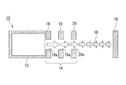
- FIG. 2A is a cross-sectional view showing an ion gun used in manufacturing the magnetic recording medium of the present invention.
- FIG. 2B is an enlarged cross-sectional view showing an ion gun used in manufacturing the magnetic recording medium of the present invention.
- FIG. 3 is a schematic configuration diagram showing an example of a magnetic recording / reproducing apparatus to which a magnetic recording medium manufactured by the manufacturing method of the present invention is applied.
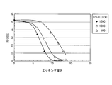
- FIG. 4 is a graph showing the relationship between the etching depth and the coercive force (Hc) when the voltage of the positive electrode is changed.
- FIG. 5 is a graph showing the relationship between the etching depth and the saturation magnetization (Ms) when the voltage of the positive electrode is changed.
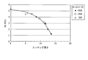
- FIG. 6 is a graph showing the relationship between the etching depth and the coercive force (Hc) when the voltage of the positive electrode is changed.
- FIG. 7 is a graph showing the relationship between the etching depth and the saturation magnetization (Ms) when the voltage of the positive electrode is changed.
- the magnetic recording medium of the present embodiment has a structure in which a soft magnetic layer, an intermediate layer, a magnetic layer with a magnetic pattern formed thereon, and a protective film are laminated on the surface of a nonmagnetic substrate, and a lubricating film is formed on the surface. Is formed.
- a lubricating film is formed on the surface.
- other than the nonmagnetic substrate and the magnetic layer may be provided as appropriate.
- the method of manufacturing a magnetic recording medium includes a step A for forming a magnetic layer 2 on a nonmagnetic substrate 1, a step B for forming a mask layer 3 on the magnetic layer 2, Step C for forming the resist layer 4 on the mask layer 3, Step D for transferring the negative pattern of the magnetic recording pattern to the resist layer 4 using the stamp 5, and making the negative pattern of the magnetic recording pattern by the mask layer 3
- a process F for modifying the magnetic properties of the lower layer 8 a process G for removing the resist layer 4 and the mask layer 3 by dry etching, and a process H for covering the surface of the magnetic layer 2 with the protective film 9 in this order. Have. Hereinafter, these steps will be described in detail.
- the magnetic layer 2 is formed on the nonmagnetic substrate 1 (step A).
- a sputtering method is used as a method of forming the magnetic layer 2, but an appropriate method may be used.
- the nonmagnetic substrate 1 used in the present embodiment include an Al alloy substrate such as an Al—Mg alloy mainly composed of Al, ordinary soda glass, aluminosilicate glass, crystallized glass, silicon, titanium, Any non-magnetic substrate such as a substrate made of ceramics or various resins can be used. Among them, it is preferable to use a glass substrate such as an Al alloy substrate or crystallized glass, or a silicon substrate.
- the average surface roughness (Ra) of these substrates is preferably 1 nm or less, more preferably 0.5 nm or less, and most preferably 0.1 nm or less.
- the magnetic layer 2 formed on the nonmagnetic substrate 1 in this embodiment may be an in-plane magnetic layer or a perpendicular magnetic layer, but a perpendicular magnetic layer is preferable in order to achieve a higher recording density.
- These magnetic layers 2 are preferably formed from an alloy mainly composed of Co.
- the magnetic layer 2 for the in-plane magnetic recording medium for example, a laminated structure composed of a nonmagnetic CrMo underlayer and a ferromagnetic CoCrPtTa magnetic layer can be used.
- Examples of the magnetic layer 2 for perpendicular magnetic recording media include soft magnetic FeCo alloys (FeCoB, FeCoSiB, FeCoZr, FeCoZrB, FeCoZrBCu, etc.), FeTa alloys (FeTaN, FeTaC, etc.), Co alloys (CoTaZr, CoZrNB, CoB, etc.). ), An orientation control film such as Pt, Pd, NiCr, NiFeCr, an intermediate film such as Ru, if necessary, and a recording made of 60Co-15Cr-15Pt alloy or 70Co-5Cr-15Pt-10SiO 2 alloy. It is possible to use a laminate of magnetic layers.
- the lower limit of the thickness of the magnetic layer 2 is preferably 3 nm, more preferably 5 nm, the upper limit is preferably 20 nm, and more preferably 15 nm.
- the magnetic layer 2 may be formed so as to obtain sufficient head input / output according to the type of magnetic alloy used and the laminated structure.
- the film thickness of the magnetic layer 2 needs to be more than a certain thickness in order to obtain a certain level of output during reproduction, while various parameters representing recording / reproduction characteristics deteriorate as the output increases. Therefore, it is necessary to set an optimum film thickness.
- the mask layer 3 formed on the magnetic layer 2 includes C, Ta, W, Cr, CrTi, Ta nitride, W nitride, Si, SiO 2 , Ta 2 O 5 , Re, Mo, Ti, V, and Nb.
- Sn, Ga, Ge, As, and Ni are preferably formed of a material containing any one or more selected from the group consisting of.
- As, Ge, Sn, and Ga are preferably used, Ni, Ti, V, and Nb are more preferably used, and Cr, C, Mo, Ta, and W are most preferably used.
- the shielding property against milling ions of the mask layer 3 can be improved, and the magnetic recording pattern forming characteristics by the mask layer 3 can be improved. Furthermore, since these materials can be easily dry-etched using a reactive gas, residues during dry etching (step G) can be reduced and contamination of the magnetic recording medium surface can be reduced.
- a resist layer 4 is formed on the mask layer 3 (step C), and a negative pattern of the magnetic recording pattern is transferred to the resist layer 4 using a stamp 5 (step D).
- the thickness 1 of the portion 11 corresponding to the negative pattern of the resist layer 4 after transferring the negative pattern of the magnetic recording pattern to the resist layer 4 is in the range of 0 to 10 nm.
- the material used for the resist layer 4 is a material that is curable by radiation irradiation, and the resist layer 4 is irradiated with radiation during the process of transferring the pattern to the resist layer 4 using the stamp 5 or after the pattern transfer process. It is preferable to do this.
- radiation refers to electromagnetic waves having a broad concept such as heat rays, visible rays, ultraviolet rays, X-rays, and gamma rays.
- the material which has curability by radiation irradiation is, for example, a thermosetting resin for heat rays and an ultraviolet curable resin for ultraviolet rays.
- the edge portion of the mask layer 3 is sagging. Can be eliminated, the shielding property of the mask layer 3 against milling ions can be improved, and the magnetic recording pattern formation characteristics by the mask layer 3 can be improved.
- the stamp 5 is pressed against the resist layer 4 in a state where the fluidity of the resist layer 4 is high, and the resist layer 4 is cured by irradiating radiation in the pressed state, and then the stamp 5 is separated from the resist layer 4.
- the shape of the stamp 5 can be accurately transferred to the resist layer 4.
- a method of irradiating radiation from the opposite side of the stamp 5, that is, the non-magnetic substrate 1 side radiation can be transmitted as a material of the stamp 5.
- a method of selecting a substance and irradiating radiation from the stamp 5 side, a method of irradiating radiation from the side of the stamp 5, a material having a high conductivity with respect to a solid such as a heat ray, or a non-magnetic substrate The method of irradiating radiation by heat conduction from 1 can be used.
- an ultraviolet curable resin such as a novolak resin, an acrylate ester, or an alicyclic epoxy is used, and as a material for the stamp 5, a glass or a resin having high transparency to ultraviolet rays is used. preferable.
- the stamp 5 can be formed by forming a fine track pattern on a metal plate using a method such as electron beam drawing, and the material is required to have hardness and durability that can withstand the process. For example, Ni or the like can be used, but any material can be used as long as it meets the above purpose.
- the stamp 5 can be formed with a servo signal pattern such as a burst pattern, a gray code pattern, and a preamble pattern in addition to a track for recording normal data.
- step E After the negative pattern of the magnetic recording pattern is transferred to the resist layer 4, the portion 11 corresponding to the negative pattern of the resist layer 4 and the portion 6 corresponding to the negative pattern of the mask layer 3 are removed by etching (step E). . Thereafter, a portion 7 of the magnetic layer 2 that is not covered with the mask layer 3 is irradiated with an ion beam 10 from the surface of the resist layer 4 to remove the upper layer portion of the magnetic layer 2 in the portion 7, and the magnetic characteristics of the lower layer portion 8 Is modified (step F).
- the range of the depth m of the upper layer portion of the magnetic layer 2 to be removed is preferably 0.1 nm, more preferably 1 nm, more preferably 15 nm, and more preferably 10 nm.
- the depth m to be removed is less than 0.1 nm, the modification effect of the lower layer portion 8 of the magnetic layer 2 does not appear, and when the depth to be removed is greater than 15 nm, the surface smoothness of the magnetic recording medium deteriorates.
- the flying characteristics of the magnetic head when the magnetic recording / reproducing apparatus is manufactured deteriorates.
- the ion beam 10 is generated using nitrogen gas or a mixed gas composed of two or more kinds of positive ions having different masses.
- the mixed gas include a mixed gas of nitrogen and hydrogen, a mixed gas of nitrogen and neon, or a mixed gas of nitrogen, hydrogen and neon.
- the range of the gas flow rate depends on the size of the reaction vessel, but in a general-sized reaction vessel, the lower limit is preferably 10 sccm, more preferably 13 sccm, most preferably 15 sccm, and the upper limit is 100 sccm. Preferably, 50 sccm is more preferable, and 35 sccm is most preferable. If it is less than 10 sccm, the discharge becomes unstable, which is disadvantageous. If it is more than 100 sccm, the etching rate is lowered, which is disadvantageous.
- the ratio of nitrogen in the entire mixed gas is preferably 63% or less, more preferably 60% or less, and most preferably 55% or less. preferable. The most effective was 50 percent. If the ratio of nitrogen is less than 35%, the etching rate is lowered, which is inconvenient. On the other hand, if it is more than 90%, the modification of the magnetic properties of the lower layer 8 becomes insufficient, which is inconvenient.
- the ratio of nitrogen in the entire mixed gas is preferably 80% or less, more preferably 70% or less, and most preferably 60% or less. preferable. The most effective was 50 percent. If the ratio of nitrogen is less than 20%, the etching rate is lowered, which is disadvantageous. On the other hand, if it is more than 80%, the modification of the magnetic properties of the lower layer 8 becomes insufficient, which is inconvenient.
- the ratio of nitrogen in the total mixed gas is preferably 90% or less, more preferably 80% or less, and 70% or less. Most preferably, the proportion of hydrogen is preferably 50 percent or less, more preferably 40 percent or less, and most preferably 30 percent or less. If the ratio of nitrogen is less than 20%, the etching rate is lowered, which is disadvantageous. On the other hand, if it is more than 90%, the modification of the magnetic properties of the lower layer 8 becomes insufficient, which is inconvenient.
- the lower limit is preferably 3.0 ⁇ 10 15 atoms / cm 2, more preferably 4.0 ⁇ 10 15 atoms / cm 2, 4.8 ⁇ 10 15 atoms / cm 2 is most preferable, and the upper limit is preferably 1.2 ⁇ 10 16 atoms / cm 2 , more preferably 1.0 ⁇ 10 16 atoms / cm 2 , and 8.0 ⁇ 10 15 atoms / cm 2. Most preferred. If it is less than 3.0 ⁇ 10 15 atoms / cm 2 , the etching rate is lowered, which is disadvantageous.
- the lower limit is preferably 0.05 nm / second, more preferably 0.07 nm / second, most preferably 0.08 nm / second, and the upper limit is preferably 2.5 nm / second.
- 0.8 nm / second is more preferable, and 1.0 nm / second is most preferable. If it is slower than 0.05 nm / second, the etching will be slow and productivity will be reduced. On the other hand, if it is faster than 2.5 nm / second, the etching is performed in a short time, and it becomes difficult to control.
- the ion gun 15 that forms the ion beam 10 includes a plasma generation chamber 13 and an electrode 14 connected to a power source (not shown).
- the electrode 14 includes a positive electrode 18, a negative electrode 19, and a ground electrode 20.
- the magnetic layer 2 and the mask layer 3 are irradiated substrates 16 that are irradiated with an ion beam 10 from a plasma generation chamber 13 that serves as an ion source.
- the positive electrode 18, the negative electrode 19, and the ground electrode 20 are provided in this order toward the nonmagnetic substrate 1 on which the resist layer 4 is laminated.
- Each of the positive electrode 18, the negative electrode 19, and the ground electrode 20 is a mesh electrode provided with openings 18a, 19a, and 20a in a mesh shape.
- the irradiated substrate 16 is omitted, but actually, the magnetic layer 2, the mask layer 3, and the resist layer 4 are provided on the nonmagnetic substrate 1 shown in FIG. It has a laminated structure, and is arranged so that the resist layer 4 side faces the ion gun 15.
- FIG. 2A shows a case where two irradiated substrates 16 are arranged and the ion beam 10 is irradiated by the left and right ion guns 15 respectively, but irradiation may be performed one by one.
- each of the openings 18a, 19a, and 20a is provided, but actually, a plurality of openings 18a, 19a, and 20a are provided in a mesh shape.
- the positive electrode 18 plays a role of pushing out ions generated in the plasma generation chamber 13 serving as an ion source toward the substrate 16 to be irradiated, and the voltage applied to the positive electrode 18 is in the range of +500 V or more and +1500 V or less. Is set.
- the negative electrode 19 plays a role of accelerating the ions pushed out by the positive electrode 18 toward the irradiated substrate 16 side, and the voltage applied to the negative electrode 19 is in the range of ⁇ 2000 V or more and ⁇ 1000 V or less. Is set in.
- the ground electrode 20 generates energy distribution when the ions generated in the plasma generation chamber 13 as an ion source, pushed out by the positive electrode 18 and accelerated by the negative electrode 19 are irradiated toward the irradiated substrate 16 side.
- the ion gun 15 configured as described above, the ion beam 10 is pushed out from the opening 18a of the positive electrode 18 and accelerated through the opening 19a of the negative electrode 19 as shown by the arrow in FIG.
- the energy distribution is made uniform by passing through the opening 20a of the electrode 20, and the substrate 16 is irradiated. Then, the ion beam 10 removes the upper layer portion of the magnetic layer 2 and modifies the magnetic properties of the lower layer portion 8.
- the modification of the magnetic layer 2 refers to partially changing the coercive force, saturation magnetization, remanent magnetization, etc. of the magnetic layer 2 in order to pattern the magnetic layer 2. Indicates that the coercive force is lowered, the saturation magnetization is lowered, and the residual magnetization is lowered.
- the saturation magnetization Ms of the magnetic layer 2 in the region 7 irradiated with the ion beam 10 is 75% or less of the initial (unprocessed), more preferably 50% or less, and the coercive force Hc is the initial value. It is preferable to adopt a method of 50% or less, more preferably 20% or less.
- the magnetic layer 2 having a magnetically separated magnetic recording pattern is formed. Since the magnetically separated magnetic recording pattern is formed, it is possible to eliminate writing blur when performing magnetic recording on the magnetic recording medium and to provide a magnetic recording medium having a high surface recording density.
- FIG. 4 and 5 show a negative electrode using an ion beam 10 generated with a mixed gas of nitrogen and hydrogen (volume ratio 1: 1) for a CoCrPt-based magnetic layer formed with a thickness of 16 nm. 19 is fixed at ⁇ 1500 V, and the positive electrode 18 voltage is changed to +500 V, +1000 V, and +1500 V, and the etching amount (etching depth) of the magnetic layer 2 and the coercive force (Hc) of the magnetic layer 2 and It is the graph which investigated the change of saturation magnetization (Ms).
- FIG. 6 and FIG. 7 are graphs when an ion beam 10 generated with argon gas instead of a mixed gas of nitrogen and hydrogen is used as a comparison. The substrates used in the experiments of FIGS.
- 4 to 7 are a glass substrate used in an example described later, a soft magnetic layer made of FeCoB having a thickness of 60 nm, a Ru intermediate layer having a thickness of 10 nm, and a Co— layer having a thickness of 12 nm.
- a layer made of a Cr—Pt—SiO 2 alloy and a 16 nm thick magnetic layer in which a 4 nm thick CoCrPt layer is laminated, and a mask layer and a resist layer are formed in the same manner as in the example, and a magnetic recording pattern The negative pattern is transferred.
- the resist layer 4 and the mask layer 3 are removed by dry etching (step G), and a nonmagnetic material is embedded in the recesses as necessary, and then the surface of the magnetic layer 2 is covered with the protective film 9. (Step H).
- dry etching is used to remove the resist layer 4 and the mask layer 3, but methods such as reactive ion etching, ion milling, and wet etching may be used.
- the protective film 9 is generally formed by a method of forming a diamond like carbon thin film using P-CVD or the like, but is not particularly limited.
- Examples of the protective film 9 include carbonaceous layers such as carbon (C), hydrogenated carbon (H x C), nitrogenated carbon (CN), amorphous carbon, silicon carbide (SiC), SiO 2 , Zr 2 O 3 , A commonly used protective film material such as TiN can be used.
- the protective film 9 may be composed of two or more layers.
- the thickness of the protective film 9 needs to be less than 10 nm. This is because if the thickness of the protective film 9 exceeds 10 nm, the distance between the head and the magnetic layer 2 increases, and sufficient input / output signal strength cannot be obtained.
- a lubricating layer on the protective film 9.
- the lubricant used for the lubricating layer include a fluorine-based lubricant, a hydrocarbon-based lubricant, and a mixture thereof, and the lubricating layer is usually formed with a thickness of 1 to 4 nm.
- the magnetically separated magnetic recording pattern referred to in the present embodiment is separated by the region 12 where the magnetic layer 2 is modified (demagnetized or weakened) when the magnetic recording medium is viewed from the surface side. Refers to the state. That is, as long as the magnetic layer 2 is separated by modification of the magnetic characteristics when viewed from the surface side, it does not have to be separated at the bottom of the magnetic layer 2, and is included in the concept of magnetically separated magnetic recording patterns.
- the modified region 12 does not have to be completely nonmagnetic. That is, even if the region 12 has a slight coercive force or saturation magnetization, a magnetically separated magnetic recording pattern can be formed if the magnetic head can read and write to the magnetic recording pattern portion. be able to.
- the magnetic recording pattern referred to in the present embodiment is a so-called patterned medium in which the magnetic recording pattern is arranged with a certain regularity for each bit, a medium in which the magnetic recording pattern is arranged in a track shape,
- servo signal patterns and the like are included.
- a step of irradiating the portion 7 of the magnetic layer 2 not covered with the mask layer 3 with the ion beam 10 to remove the upper layer portion of the portion 7 and modifying the magnetic characteristics of the lower layer portion 8 is adopted.
- the ion beam 10 processes only the upper layer portion of the magnetic layer 2, the amount of processing is small, and the generation of dust can be suppressed. As a result, a magnetic recording medium having a clean and smooth surface can be obtained.
- the removal of the upper layer portion of the magnetic layer 2 and the step of modifying the magnetic properties of the lower layer portion 8 can be performed simultaneously. It can be performed with high efficiency. Further, since the ion beam 10 does not contain a halogen, no halide is generated, and therefore, the halide does not corrode on the basis of contact with the atmosphere.
- the ion gun 15 forming the ion beam 10 has a ground electrode 20 that stabilizes the energy distribution of ions from the plasma generation chamber 13 that is an ion source, and the electrode 14 of the ion gun 15 is irradiated from the plasma generation chamber 13.
- the positive electrode 18, the negative electrode 19, and the ground electrode 20 are provided in this order toward the substrate 16 side.
- the upper layer portion of the magnetic layer 2 can be removed and the lower layer can be removed. It is possible to irradiate the ion beam 10 that is accurately adapted to the purpose of modifying the magnetic characteristics of the unit 8.
- the positive electrode 18, the negative electrode 19 and the ground electrode 20 are all mesh electrodes, the irradiation amount of the ion beam 10 is made uniform in the irradiated portion, and the upper layer portion and the lower layer portion are removed. Thus, the modification of the magnetic characteristics can be performed with high accuracy.
- FIG. 3 shows an example of a magnetic recording / reproducing apparatus using the magnetic recording medium described above.
- the magnetic recording / reproducing apparatus shown in FIG. 3 includes the magnetic recording medium 21 described above, a medium driving unit 22 that drives the magnetic recording medium 21 in the recording direction, a magnetic head 23 that includes a recording unit and a reproducing unit, and a magnetic head 23 that is And a recording / reproduction signal system 25 that combines recording / reproduction signal processing means for reproducing a signal input to the magnetic head 23 and reproducing an output signal from the magnetic head 23.
- a medium driving unit 22 that drives the magnetic recording medium 21 in the recording direction
- a magnetic head 23 that includes a recording unit and a reproducing unit
- a magnetic head 23 that is And a recording / reproduction signal system 25 that combines recording / reproduction signal processing means for reproducing a signal input to the magnetic head 23 and reproducing an output signal from the magnetic head 23.
- the reproducing head width is made narrower than the recording head width. Can be operated with both of them approximately the same width. As a result, sufficient reproduction output and high SNR can be obtained.
- the reproducing unit of the magnetic head 23 by configuring the reproducing unit of the magnetic head 23 with a GMR head or a TMR head, a sufficient signal intensity can be obtained even at a high recording density, and a magnetic recording apparatus having a high recording density can be realized. Further, when the flying height of the magnetic head 23 is 0.005 ⁇ m to 0.020 ⁇ m, the output is improved and a high device SNR is obtained, and a large capacity and high reliability magnetic recording apparatus is obtained. Can be provided. Further, when the signal processing circuit based on the maximum likelihood decoding method is combined, the recording density can be further improved. For example, the track density is 100 ktrack / inch or more, the linear recording density is 1000 kbit / inch or more, and the recording density is 100 Gbit or more per square inch. A sufficient SNR can also be obtained when recording / reproducing.
- the vacuum chamber in which the glass substrate for HD was set was evacuated to 1.0 ⁇ 10 ⁇ 5 Pa or less in advance.
- the glass substrate used here is composed of Li 2 Si 2 O 5 , Al 2 O 3 —K 2 O, Al 2 O 3 —K 2 O, MgO—P 2 O 5 , Sb 2 O 3 —ZnO. It is made of crystallized glass and has an outer diameter of 65 mm, an inner diameter of 20 mm, and an average surface roughness (Ra) of 2 angstroms.
- thin films were laminated in this order of FeCoB as the soft magnetic layer, Ru as the intermediate layer, and 70Co-5Cr-15Pt-10SiO 2 alloy as the magnetic layer.
- the thickness of each layer was 60 nm for the FeCoB soft magnetic layer, 10 nm for the Ru intermediate layer, and 15 nm for the magnetic layer.
- a mask layer was formed thereon using a sputtering method, and C was used for the mask layer to a thickness of 20 nm.
- a resist layer was applied by spin coating.
- a novolac resin which is an ultraviolet curable resin, was used.
- the film thickness was 60 nm.
- a stamp made of glass having a negative pattern of a magnetic recording pattern was further pressed against the resist layer at a pressure of 1 MPa (about 8.8 kgf / cm 2 ).
- ultraviolet rays having a wavelength of 250 nm were irradiated for 10 seconds from the top of a glass stamp having an ultraviolet transmittance of 95% or more to cure the resist.
- the stamp was separated from the resist layer, and the magnetic recording pattern was transferred.
- the convex portion of the resist layer has a circumferential shape with a width of 64 nm
- the concave portion of the resist layer (the portion corresponding to the negative pattern) has a circumferential shape with a width of 30 nm.
- the angle of the concave portion of the resist layer with respect to the substrate surface was approximately 90 degrees.
- the dry etching conditions are as follows: O 2 gas is 40 sccm, pressure is 0.3 Pa, high frequency plasma power is 300 W, DC bias is 30 W, etching time is 10 seconds for resist etching, and O 2 gas is 50 sccm for etching the C layer.
- the pressure was 0.6 Pa
- the high-frequency plasma power was 500 W
- the DC bias was 60 W
- the etching time was 30 seconds.
- the surface of the portion not covered with the mask layer with the magnetic layer was irradiated with an ion beam.
- the ion beam was generated using a mixed gas of nitrogen gas 40 sccm, hydrogen gas 20 sccm, and neon 20 sccm.
- the amount of ions is 5.5 ⁇ 10 15 atoms / cm 2
- the etching rate is 0.1 nm / second
- the positive electrode voltage is +1500 V
- the negative electrode voltage is ⁇ 1500 V
- the etching time is 84 seconds
- the magnetic layer The processing depth was 8 nm.
- the resist layer and the mask layer were removed by dry etching, a 4 nm carbon protective film was formed on the surface by CVD, and then a lubricant was applied to 1.5 nm to produce a magnetic recording medium.
- the electromagnetic conversion characteristics (SNR and 3T-squash) and the head flying height (glide avalanche) of the magnetic recording medium manufactured by the above method were measured.
- “3T-squash (triple track squash)” refers to signal deterioration of the center track when writing on both adjacent tracks.
- Evaluation of electromagnetic conversion characteristics was performed using a spin stand. At this time, the SNR value and 3T-squash when a 750 kFCI signal was recorded were measured using a perpendicular recording head for recording and a TuMR head for reading.
- the manufactured magnetic recording medium had an SNR of 13.7 dB and 3T-square of 86%, excellent RW characteristics, and stable head flying characteristics. That is, the smoothness of the surface of the magnetic recording medium was high, and the separation characteristics by the nonmagnetic part between the tracks of the magnetic layer were excellent.
- the present invention can be widely used in the manufacturing industry for manufacturing magnetic recording media.
Landscapes
- Manufacturing Of Magnetic Record Carriers (AREA)
- Magnetic Record Carriers (AREA)
- Drying Of Semiconductors (AREA)
Abstract
Description
本願は、2009年3月11日に、日本に出願された特願2009-58116号に基づき優先権を主張し、その内容をここに援用する。
また、近年では線記録密度の向上と同時にトラック密度の増加によって面記録密度を上昇させようとする努力も続けられている。特に、最新の磁気記録装置においてはトラック密度が110kTPIにも達している。
また、同一トラック内のデータ領域を更に分割した、いわゆるパターンドメディアを製造しようとする試みもある。
この磁気記録媒体によれば、軟磁性層での磁壁発生を抑制できるため熱揺らぎの影響が出にくく、隣接する信号間の干渉もないので、ノイズの少ない高密度磁気記録媒体を形成できるとされている。
(1)磁気的に分離した磁気記録パターンを有する磁気記録媒体の製造方法であって、
非磁性基板上に磁性層を形成する工程と、磁性層の上に磁気記録パターンを形成するためのマスク層を形成する工程と、磁性層のマスク層に覆われていない部位にイオンビームを照射し、該部位の磁性層の上層部を除去すると共に、下層部の磁気特性を改質する工程をこの順で有し、イオンビームには、質量の異なる2種以上の正イオンを使用し、イオンビームを形成するイオンガンが、イオン源からの正イオンを基板側に押し出す正電極と、正イオンを基板側に加速させる負電極を有することを特徴とする磁気記録媒体の製造方法。
(2)質量の異なる2種以上の前記正イオンが、窒素と水素またはネオンを含むイオンであることを特徴とする(1)に記載の磁気記録媒体の製造方法。
(3)前記イオンガンが、前記イオン源からの前記正イオンのエネルギー分布を安定させる接地電極を有し、前記イオンガンの電極が、前記イオン源から前記基板側に、正電極、負電極、接地電極の順で設けられていることを特徴とする(1)または(2)に記載の磁気記録媒体の製造方法。
(4)前記正電極への印加電圧が、+500V以上+1500V以下の範囲内であり、前記負電極への印加電圧が、-2000V以上-1000V以下の範囲内であることを特徴とする(1)ないし(3)の何れかに記載の磁気記録媒体の製造方法。
(5)前記イオンガンの電極が、網目状電極であることを特徴とする(1)ないし(4)の何れかに記載の磁気記録媒体の製造方法。
(6)(1)ないし(5)の何れかに記載の製造方法により得られた磁気記録媒体と、該磁気記録媒体に情報を記録再生する磁気ヘッドを具備してなることを特徴とする磁気記録再生装置。
また、イオンビームを形成するイオンガンが、イオン源からの正イオンを基板側に押し出す正電極と、正イオンを基板側に加速する負電極とを有している。これにより、層部の除去及び下層部の磁気特性の改質を行うという目的に適合したイオンビームを照射することができ、精度良く磁性層の上層部の除去及び下層部の磁気特性の改質を行うことができる。
なお、本実施形態の磁気記録媒体は、非磁性基板の表面に軟磁性層、中間層、磁気パターンが形成された磁性層、保護膜を積層した構造を有し、さらに表面には潤滑膜が形成されている。もっとも、非磁性基板及び磁性層以外は適宜設けて構わない。
通常、磁性層2を形成する方法としてはスパッタ法を用いるが、適宜の方法で構わない。
本実施形態で使用する非磁性基板1としては、Alを主成分とした例えばAl-Mg合金等のAl合金基板や、通常のソーダガラス、アルミノシリケート系ガラス、結晶化ガラス類、シリコン、チタン、セラミックス、各種樹脂からなる基板など、非磁性基板であれば任意のものを用いることができる。中でもAl合金基板や結晶化ガラス等のガラス製基板又はシリコン基板を用いることが好ましい。
また、これら基板の平均表面粗さ(Ra)は、1nm以下であることが好ましく、0.5nm以下であることがより好ましく、0.1nm以下であることが最も好ましい。
また、磁性層2は使用する磁性合金の種類と積層構造に合わせて、十分なヘッド出入力が得られるように形成すればよい。
磁性層2の膜厚は、再生の際に一定以上の出力を得るためにはある程度以上の厚さであることが必要であり、一方で記録再生特性を表す諸パラメーターは出力の上昇とともに劣化するのが通例であるため、最適な膜厚に設定する必要がある。
磁性層2の上に形成するマスク層3は、C、Ta、W、Cr、CrTi、Ta窒化物、W窒化物、Si、SiO2、Ta2O5、Re、Mo、Ti、V、Nb、Sn、Ga、Ge、As、Niからなる群から選ばれた何れか一種以上を含む材料で形成するのが好ましい。特に、As、Ge、Sn、Gaを用いるのが好ましく、Ni、Ti、V、Nbを用いるのがより好ましく、Cr、C、Mo、Ta、Wを用いるのが最も好ましい。
この際、レジスト層4に磁気記録パターンのネガパターンを転写した後の、レジスト層4のネガパターンに対応する部位11の厚さlを、0~10nmの範囲内とするのが好ましい。
レジスト層4の部位11の厚さlをこの範囲とすることにより、マスク層3のエッチング工程(工程E)において、マスク層3のエッジの部分のダレを無くし、マスク層3のミリングイオンに対する遮蔽性を向上させ、また、マスク層3による磁気記録パターン形成特性を向上させることができる。
ここでいう放射線とは、熱線、可視光線、紫外線、X線、ガンマ線等の広い概念の電磁波である。また、放射線照射により硬化性を有する材料とは、例えば、熱線に対しては熱硬化樹脂、紫外線に対しては紫外線硬化樹脂である。
また、レジスト層4の材料としてノボラック系樹脂、アクリル酸エステル類、脂環式エポキシ類等の紫外線硬化樹脂を用い、スタンプ5の材料として紫外線に対して透過性の高いガラスもしくは樹脂を用いるのが好ましい。
その後、レジスト層4側表面から磁性層2のマスク層3に覆われていない部位7にイオンビーム10を照射し、部位7の磁性層2の上層部を除去すると共に、下層部8の磁気特性を改質する(工程F)。
除去する深さmが0.1nmより少ない場合は、磁性層2の下層部8の改質効果が現れず、また、除去する深さが15nmより大きくなると、磁気記録媒体の表面平滑性が悪化し、磁気記録再生装置を製造した際の磁気ヘッドの浮上特性が悪くなる。
ガスの流量の範囲としては、反応容器の大きさにもよるが、一般的な大きさの反応容器では、下限が、10sccmが好ましく、13sccmがより好ましく、15sccmが最も好ましく、上限が、100sccmが好ましく、50sccmがより好ましく、35sccmが最も好ましい。
10sccmより少ないと、放電が不安定となって不都合があり、100sccmより多いと、エッチングレートが低下することとなって不都合がある。
窒素の割合が、35パーセントより少ないと、エッチングレートが低下することとなり、不都合がある。また、90パーセントより多いと、下層部8の磁気特性の改質が不十分となり、不都合がある。
窒素の割合が、20パーセントより少ないと、エッチングレートが低下することとなり、不都合がある。また、80パーセントより多いと、下層部8の磁気特性の改質が不十分となり、不都合がある。
窒素の割合が、20パーセントより少ないと、エッチングレートが低下することとなり、不都合がある。また、90パーセントより多いと、下層部8の磁気特性の改質が不十分となり、不都合がある。
3.0×10¹⁵原子/cm2より少ないと、エッチングレートが低下することとなり、不都合がある。また、1.2×1016原子/cm2より多いと、マスク層3のダメージが大きくなり、磁性層2の改質させる必要のない部位まで磁気特性が劣化する恐れがあり、不都合となる。
0.05nm/秒より遅いと、エッチングが遅くなり、生産性が低下することとなる。また、2.5nm/秒より早いと、エッチングが短時間で行われることとなり、制御するのが難しくなる。
電極14は、正電極18、負電極19、接地電極20から構成されており、イオン源となるプラズマ発生室13から、イオンビーム10を照射させる被照射基板16である磁性層2、マスク層3、レジスト層4が積層された非磁性基板1側に向かって、正電極18、負電極19、接地電極20の順で設けられている。
正電極18、負電極19、接地電極20は、いずれも網目状に開口部18a、19a、20aが設けられた網目状電極である。
なお、図2A、図2Bでは、被照射基板16を省略して示しているが、実際には、図1(E)に示す非磁性基板1に磁性層2、マスク層3、レジスト層4が積層された構成をしており、レジスト層4側がイオンガン15に対向するように配置されている。また、図2Aでは、被照射基板16を2枚配置し、それぞれ左右のイオンガン15によってイオンビーム10が照射される場合について示しているが、1枚ずつ照射しても構わない。また、図2Bでは、開口部18a、19a、20aがそれぞれ1つずつ設けられているが、実際には、網目状に複数設けられている。
また、負電極19は、正電極18によって押し出されたイオンを、被照射基板16側に向かって加速させる役割を担っており、負電極19への印加電圧は、-2000V以上-1000V以下の範囲内に設定されている。
以上のような構成をしたイオンガン15によって、イオンビーム10は、図2Bの矢印で示すように、正電極18の開口部18aから押し出され、負電極19の開口部19aを通って加速され、接地電極20の開口部20aを通ることでエネルギー分布が均一化して、被照射基板16に照射される。そして、イオンビーム10により、磁性層2の上層部が除去されると共に、下層部8の磁気特性が改質される。
なお、図4ないし図7の実験に用いた基板は、後述する実施例で使用するガラス基板上に60nm厚のFeCoBからなる軟磁性層と、10nm厚のRu中間層と、12nm厚のCo-Cr-Pt-SiO2合金からなる層と4nm厚のCoCrPt層とが積層された16nm厚の磁性層とを積層し、更に実施例と同様にしてマスク層及びレジスト層が形成され、磁気記録パターンのネガパターンが転写されたものである。
これに対し、正電極18の電圧が+1500Vの場合は、エッチングの深さを10nmとした際(残りの磁性層は5nm)、保磁力(Hc)は略0となり、飽和磁化(Ms)は3分の1程度となっていることが分かる。
なお、図6及び図7が示すように、アルゴンガスで発生させたイオンビーム10を用いた場合には、正電極18の電圧を変化させても、エッチングの深さが変化しても磁気特性の改質がほとんど認められない。
なお、正電極18の電圧を+1500Vより高めた場合や、負電極19の電圧を-2000Vよりも下げた場合は、イオンの注入深さが深くなりすぎ、例えば垂直磁気記録媒体用の磁性層2の場合では、軟磁性の裏打ち層までイオンが到達することとなる。その結果、裏打ち層等の磁気特性が悪化し、磁気記録媒体にスパイクノイズが発生することとなり、好ましくない。
保護膜9としては、炭素(C)、水素化炭素(HxC)、窒素化炭素(CN)、アルモファスカーボン、炭化珪素(SiC)等の炭素質層やSiO2、Zr2O3、TiNなど、通常用いられる保護膜材料を用いることができる。
ただし、保護膜9の膜厚は10nm未満とする必要がある。保護膜9の膜厚が10nmを越えるとヘッドと磁性層2との距離が大きくなり、十分な出入力信号の強さが得られなくなるからである。
なお、本実施形態でいう磁気的に分離した磁気記録パターンとは、磁気記録媒体を表面側から見た場合、磁性層2が改質(非磁性化または弱磁性化)した領域12により分離された状態を指す。すなわち、磁性層2が表面側から見て磁気特性の改質により分離されていれば、磁性層2の底部において分離されていなくともよく、磁気的に分離した磁気記録パターンの概念に含まれる。
この中で特に、磁気的に分離した磁気記録パターンが、磁気記録トラック及びサーボ信号パターンである、いわゆる、ディスクリート型磁気記録媒体に適用するのが、その製造における簡便性から好ましい。
図3に示す磁気記録再生装置は、上述した磁気記録媒体21と、これを記録方向に駆動する媒体駆動部22と、記録部と再生部からなる磁気ヘッド23と、磁気ヘッド23を磁気記録媒体21に対して相対運動させるヘッド駆動部24と、磁気ヘッド23への信号入力と磁気ヘッド23からの出力信号再生を行うための記録再生信号処理手段を組み合わせた記録再生信号系25とを具備して構成されている。
磁気記録媒体21の記録トラックを磁気的に不連続に加工したことによって、従来はトラックエッジ部の磁化遷移領域の影響を排除するために再生ヘッド幅を記録ヘッド幅よりも狭くして対応していたものを、両者をほぼ同じ幅にして動作させることができる。これにより十分な再生出力と高いSNRを得ることができるようになる。
また、この磁気ヘッド23の浮上量を0.005μm~0.020μmと従来より低い高さで浮上させると、出力が向上して高い装置SNRが得られ、大容量で高信頼性の磁気記録装置を提供することができる。更に、最尤復号法による信号処理回路を組み合わせるとさらに記録密度を向上でき、例えば、トラック密度100kトラック/インチ以上、線記録密度1000kビット/インチ以上、1平方インチ当たり100Gビット以上の記録密度で記録・再生する場合にも十分なSNRが得られる。
[実施例]
HD用ガラス基板をセットした真空チャンバをあらかじめ1.0×10⁻⁵Pa以下に真空排気した。ここで使用したガラス基板はLi2Si2O5、Al2O3-K2O、Al2O3-K2O、MgO-P2O5、Sb2O3-ZnOを構成成分とする結晶化ガラスを材質とし、外径65mm、内径20mm、平均表面粗さ(Ra)は2オングストロームである。
その上に、レジスト層をスピンコート法により塗布した。レジスト層には、紫外線硬化樹脂であるノボラック系樹脂を用いた。また膜厚は60nmとした。
その後、レジスト層及びマスク層をドライエッチングにより除去し、その表面にCVD法にてカーボン保護膜を4nm成膜し、その後、潤滑剤を1.5nm塗布して磁気記録媒体を製造した。
(残存信号強度Vp-p)/(元々の信号強度Vp-p)×100(%)
で表現する。この値が、100%に近ければ近いほど耐隣接書き込みが強いと評価される。
電磁変換特性の評価はスピンスタンドを用いて実施した。このとき評価用のヘッドには、記録には垂直記録ヘッド、読み込みにはTuMRヘッドを用いて、750kFCIの信号を記録したときのSNR値および3T-squashを測定した。
製造された磁気記録媒体は、SNRが13.7dB、3T-squashが86%でありRW特性に優れ、また、ヘッド浮上特性も安定していた。すなわち、磁気記録媒体表面の平滑性が高く、磁性層のトラック間の非磁性部による分離特性が優れていた。
2・・・磁性層、
3・・・マスク層、
4・・・レジスト層、
5・・・スタンプ、
6・・・マスク層のネガパターンに対応する部位、
7・・・磁性層のマスク層に覆われていない部位、
8・・・下層部、
10・・・イオンビーム、
11・・・レジスト層のネガパターンに対応する部位、
12・・・磁性層のネガパターンに対応する部位、
13・・・プラズマ発生室、
14・・・電極、
15・・・イオンガン、
18・・・正電極、
19・・・負電極、
20・・・接地電極、
21・・・磁気記録媒体
Claims (6)
- 磁気的に分離した磁気記録パターンを有する磁気記録媒体の製造方法であって、
非磁性基板上に磁性層を形成する工程と、
磁性層の上に磁気記録パターンを形成するためのマスク層を形成する工程と、
磁性層のマスク層に覆われていない部位にイオンビームを照射し、該部位の磁性層の上層部を除去すると共に、下層部の磁気特性を改質する工程をこの順で有し、
イオンビームには、質量の異なる2種以上の正イオンを使用し、
イオンビームを形成するイオンガンが、イオン源からの正イオンを基板側に押し出す正電極と、正イオンを基板側に加速させる負電極を有することを特徴とする磁気記録媒体の製造方法。 - 質量の異なる2種以上の前記正イオンが、窒素と水素またはネオンを含むイオンであることを特徴とする請求項1に記載の磁気記録媒体の製造方法。
- 前記イオンガンが、前記イオン源からの前記正イオンのエネルギー分布を安定させる接地電極を有し、
前記イオンガンの電極が、前記イオン源から前記基板側に、正電極、負電極、接地電極の順で設けられていることを特徴とする請求項1または請求項2に記載の磁気記録媒体の製造方法。 - 前記正電極への印加電圧が、+500V以上+1500V以下の範囲内であり、
前記負電極への印加電圧が、-2000V以上-1000V以下の範囲内であることを特徴とする請求項1または請求項2に記載の磁気記録媒体の製造方法。 - 前記イオンガンの電極が、網目状電極であることを特徴とする請求項1または請求項2に記載の磁気記録媒体の製造方法。
- 請求項1または請求項2に記載の製造方法により得られた磁気記録媒体と、
該磁気記録媒体に情報を記録再生する磁気ヘッドを具備してなることを特徴とする磁気記録再生装置。
Priority Applications (2)
| Application Number | Priority Date | Filing Date | Title |
|---|---|---|---|
| CN201080011288.2A CN102349103B (zh) | 2009-03-11 | 2010-03-08 | 磁记录介质的制造方法和磁记录再生装置 |
| US13/255,450 US20120044596A1 (en) | 2009-03-11 | 2010-03-08 | Method of producing magnetic recording medium and magnetic recording and reproducing apparatus |
Applications Claiming Priority (2)
| Application Number | Priority Date | Filing Date | Title |
|---|---|---|---|
| JP2009058116A JP5427441B2 (ja) | 2009-03-11 | 2009-03-11 | 磁気記録媒体の製造方法 |
| JP2009-058116 | 2009-03-11 |
Publications (1)
| Publication Number | Publication Date |
|---|---|
| WO2010103785A1 true WO2010103785A1 (ja) | 2010-09-16 |
Family
ID=42728081
Family Applications (1)
| Application Number | Title | Priority Date | Filing Date |
|---|---|---|---|
| PCT/JP2010/001611 Ceased WO2010103785A1 (ja) | 2009-03-11 | 2010-03-08 | 磁気記録媒体の製造方法、および磁気記録再生装置 |
Country Status (4)
| Country | Link |
|---|---|
| US (1) | US20120044596A1 (ja) |
| JP (1) | JP5427441B2 (ja) |
| CN (1) | CN102349103B (ja) |
| WO (1) | WO2010103785A1 (ja) |
Families Citing this family (4)
| Publication number | Priority date | Publication date | Assignee | Title |
|---|---|---|---|---|
| US10202684B2 (en) | 2010-08-23 | 2019-02-12 | Exogenesis Corporation | Method for neutral beam processing based on gas cluster ion beam technology and articles produced thereby |
| JP5698952B2 (ja) * | 2010-10-22 | 2015-04-08 | 昭和電工株式会社 | 磁気記録媒体の製造方法及び磁気記録再生装置 |
| CN114899096A (zh) * | 2015-10-14 | 2022-08-12 | 艾克索乔纳斯公司 | 使用基于气体团簇离子束技术的中性射束处理的超浅蚀刻方法以及由此产生的物品 |
| JP7377182B2 (ja) * | 2020-09-25 | 2023-11-09 | 富士フイルム株式会社 | 磁気記録ヘッドおよびその製造方法、磁気記録装置ならびに磁気記録媒体の製造方法 |
Citations (6)
| Publication number | Priority date | Publication date | Assignee | Title |
|---|---|---|---|---|
| JPH11161947A (ja) * | 1997-11-27 | 1999-06-18 | Kao Corp | 磁気記録媒体の製造方法 |
| JP2008117753A (ja) * | 2006-10-12 | 2008-05-22 | Tdk Corp | イオンガン、イオンビームエッチング装置、イオンビームエッチング設備、エッチング方法及び磁気記録媒体の製造方法 |
| JP2008293573A (ja) * | 2007-05-23 | 2008-12-04 | Toshiba Corp | 磁気記録媒体およびその製造方法 |
| JP2009170007A (ja) * | 2008-01-11 | 2009-07-30 | Toshiba Corp | 磁気記録媒体の製造方法 |
| JP2009181673A (ja) * | 2008-01-31 | 2009-08-13 | Toshiba Corp | 磁気記録媒体の製造方法 |
| JP2010049752A (ja) * | 2008-08-22 | 2010-03-04 | Toshiba Corp | 磁気記録媒体の製造方法 |
Family Cites Families (6)
| Publication number | Priority date | Publication date | Assignee | Title |
|---|---|---|---|---|
| US3904505A (en) * | 1970-03-20 | 1975-09-09 | Space Sciences Inc | Apparatus for film deposition |
| US6864042B1 (en) * | 2000-07-25 | 2005-03-08 | Seagate Technology Llc | Patterning longitudinal magnetic recording media with ion implantation |
| US20030099069A1 (en) * | 2001-10-10 | 2003-05-29 | Tdk Corporation | Magnetic head, method of manufacturing same, and head suspension assembly |
| JP2004164692A (ja) * | 2002-11-08 | 2004-06-10 | Toshiba Corp | 磁気記録媒体及びその製造方法 |
| US7230795B2 (en) * | 2003-03-27 | 2007-06-12 | Tdk Corporation | Recording medium having reduced surface roughness |
| US6975073B2 (en) * | 2003-05-19 | 2005-12-13 | George Wakalopulos | Ion plasma beam generating device |
-
2009
- 2009-03-11 JP JP2009058116A patent/JP5427441B2/ja active Active
-
2010
- 2010-03-08 WO PCT/JP2010/001611 patent/WO2010103785A1/ja not_active Ceased
- 2010-03-08 US US13/255,450 patent/US20120044596A1/en not_active Abandoned
- 2010-03-08 CN CN201080011288.2A patent/CN102349103B/zh active Active
Patent Citations (6)
| Publication number | Priority date | Publication date | Assignee | Title |
|---|---|---|---|---|
| JPH11161947A (ja) * | 1997-11-27 | 1999-06-18 | Kao Corp | 磁気記録媒体の製造方法 |
| JP2008117753A (ja) * | 2006-10-12 | 2008-05-22 | Tdk Corp | イオンガン、イオンビームエッチング装置、イオンビームエッチング設備、エッチング方法及び磁気記録媒体の製造方法 |
| JP2008293573A (ja) * | 2007-05-23 | 2008-12-04 | Toshiba Corp | 磁気記録媒体およびその製造方法 |
| JP2009170007A (ja) * | 2008-01-11 | 2009-07-30 | Toshiba Corp | 磁気記録媒体の製造方法 |
| JP2009181673A (ja) * | 2008-01-31 | 2009-08-13 | Toshiba Corp | 磁気記録媒体の製造方法 |
| JP2010049752A (ja) * | 2008-08-22 | 2010-03-04 | Toshiba Corp | 磁気記録媒体の製造方法 |
Also Published As
| Publication number | Publication date |
|---|---|
| JP2010211879A (ja) | 2010-09-24 |
| US20120044596A1 (en) | 2012-02-23 |
| CN102349103B (zh) | 2014-09-17 |
| CN102349103A (zh) | 2012-02-08 |
| JP5427441B2 (ja) | 2014-02-26 |
Similar Documents
| Publication | Publication Date | Title |
|---|---|---|
| JP2008135092A (ja) | 磁気記録媒体の製造方法、及び磁気記録再生装置 | |
| JP4597933B2 (ja) | 磁気記録媒体の製造方法、並びに磁気記録再生装置 | |
| JP2008052860A (ja) | 磁気記録媒体の製造方法、及び磁気記録再生装置 | |
| JP5478251B2 (ja) | 磁気記録媒体の製造方法 | |
| JP4843825B2 (ja) | 磁気記録媒体の製造方法及び磁気記録再生装置 | |
| JP5398163B2 (ja) | 磁気記録媒体及びその製造方法、並びに磁気記録再生装置 | |
| JP2010140544A (ja) | 磁気記録媒体の製造方法及び磁気記録媒体、並びに磁気記録再生装置 | |
| JP5427441B2 (ja) | 磁気記録媒体の製造方法 | |
| JP5186345B2 (ja) | 磁気記録媒体の製造方法 | |
| JP5431678B2 (ja) | 磁気記録媒体の製造方法、磁気記録媒体、及び磁気記録再生装置 | |
| WO2009081932A1 (ja) | 磁気記録媒体の製造方法および磁気記録再生装置 | |
| JP4634354B2 (ja) | 磁気記録媒体の製造方法 | |
| JP5334865B2 (ja) | 磁気記録媒体の製造方法および磁気記録再生装置 | |
| JP5383050B2 (ja) | 磁気記録媒体の製造方法及び磁気記録再生装置 | |
| US8828483B2 (en) | Manufacturing method for magnetic recording medium, magnetic recording/reproducing device | |
| JP5698952B2 (ja) | 磁気記録媒体の製造方法及び磁気記録再生装置 | |
| JP2010140541A (ja) | 磁気記録媒体の製造方法及び磁気記録媒体、並びに磁気記録再生装置 | |
| WO2010058548A1 (ja) | 磁気記録媒体の製造方法及び磁気記録再生装置 | |
| JP2011023081A (ja) | 磁気記録媒体の製造方法及び磁気記録再生装置 | |
| WO2011077943A1 (ja) | 磁気記録媒体の製造方法及び磁気記録再生装置 | |
| JP2010152978A (ja) | 磁気記録媒体及びその製造方法、並びに磁気記録再生装置 | |
| WO2011087078A1 (ja) | 磁気記録媒体の製造方法及び磁気記録再生装置 |
Legal Events
| Date | Code | Title | Description |
|---|---|---|---|
| WWE | Wipo information: entry into national phase |
Ref document number: 201080011288.2 Country of ref document: CN |
|
| 121 | Ep: the epo has been informed by wipo that ep was designated in this application |
Ref document number: 10750543 Country of ref document: EP Kind code of ref document: A1 |
|
| NENP | Non-entry into the national phase |
Ref country code: DE |
|
| WWE | Wipo information: entry into national phase |
Ref document number: 13255450 Country of ref document: US |
|
| 122 | Ep: pct application non-entry in european phase |
Ref document number: 10750543 Country of ref document: EP Kind code of ref document: A1 |