WO2010103741A1 - 過電圧抑制装置 - Google Patents
過電圧抑制装置 Download PDFInfo
- Publication number
- WO2010103741A1 WO2010103741A1 PCT/JP2010/001371 JP2010001371W WO2010103741A1 WO 2010103741 A1 WO2010103741 A1 WO 2010103741A1 JP 2010001371 W JP2010001371 W JP 2010001371W WO 2010103741 A1 WO2010103741 A1 WO 2010103741A1
- Authority
- WO
- WIPO (PCT)
- Prior art keywords
- voltage
- waveform
- circuit breaker
- transmission line
- overvoltage
- Prior art date
- Legal status (The legal status is an assumption and is not a legal conclusion. Google has not performed a legal analysis and makes no representation as to the accuracy of the status listed.)
- Ceased
Links
Images









Classifications
-
- H—ELECTRICITY
- H01—ELECTRIC ELEMENTS
- H01H—ELECTRIC SWITCHES; RELAYS; SELECTORS; EMERGENCY PROTECTIVE DEVICES
- H01H9/00—Details of switching devices, not covered by groups H01H1/00 - H01H7/00
- H01H9/54—Circuit arrangements not adapted to a particular application of the switching device and for which no provision exists elsewhere
- H01H9/56—Circuit arrangements not adapted to a particular application of the switching device and for which no provision exists elsewhere for ensuring operation of the switch at a predetermined point in the AC cycle
- H01H9/563—Circuit arrangements not adapted to a particular application of the switching device and for which no provision exists elsewhere for ensuring operation of the switch at a predetermined point in the AC cycle for multipolar switches, e.g. different timing for different phases, selecting phase with first zero-crossing
-
- H—ELECTRICITY
- H01—ELECTRIC ELEMENTS
- H01H—ELECTRIC SWITCHES; RELAYS; SELECTORS; EMERGENCY PROTECTIVE DEVICES
- H01H33/00—High-tension or heavy-current switches with arc-extinguishing or arc-preventing means
- H01H33/02—Details
- H01H33/59—Circuit arrangements not adapted to a particular application of the switch and not otherwise provided for, e.g. for ensuring operation of the switch at a predetermined point in the AC cycle
- H01H33/593—Circuit arrangements not adapted to a particular application of the switch and not otherwise provided for, e.g. for ensuring operation of the switch at a predetermined point in the AC cycle for ensuring operation of the switch at a predetermined point of the AC cycle
Definitions
- This invention relates to the overvoltage suppression apparatus which suppresses the overvoltage which arises when throwing a circuit breaker.
- a breaker with a resistor as a method of suppressing an overvoltage when the no-load transmission line is turned on.
- a resistor insertion type circuit breaker is employed to suppress such an overvoltage.
- the circuit breaker with a resistor has a configuration in which an input resistor and a contact are connected in series.
- the breaker with a resistor is connected in parallel with the breaker main contact.
- the circuit breaker with a resistor is inserted before the main contact of the circuit breaker. Thereby, overvoltage is suppressed (for example, refer nonpatent literature 1 of Japan).
- the transmission line in the no-load transmission line compensated by the reactor, after the breaker breaks, the transmission line generates an oscillating voltage due to its capacitance and the reactor. Even in such a case, if the circuit breaker is turned on again when the voltage between the electrodes of the circuit breaker is large, an overvoltage is generated.
- a method for suppressing overvoltage when a power transmission line compensated by a reactor is turned on again a method of controlling the circuit breaker closing phase is known. In this case, the circuit breaker is restarted when the voltage between the electrodes is small. The following is known as a method for predicting the time point at which the interelectrode voltage decreases.
- the power supply (side) voltage is a sine wave of commercial frequency. Further, if the oscillation voltage on the line side is also a single frequency, it can be regarded as a sine wave. These two voltages are approximated by a function of a sine wave to predict the interelectrode voltage. Based on this inter-electrode voltage, the closing time of the circuit breaker is determined (see, for example, Patent Document 1 in Japan).
- a method is disclosed in which the circuit breaker is inserted at a future inter-pole voltage zero by measuring the time between the inter-pole voltage zeros of the circuit breaker. The time between the voltage zero points of one cycle of the interpolar voltage after the interruption and the voltage zero point of the next cycle of the interpolar voltage is measured. If the time between these two inter-electrode voltage zeros is the same, the frequency of the inter-electrode voltage is known. Thereby, the future inter-electrode voltage zero can be estimated regardless of the inter-electrode voltage waveform (see, for example, Non-Patent Document 2).
- a reactor may be installed on the transmission line to compensate for its reactive power.
- the circuit breaker opens the power transmission line on which the reactor is installed, a voltage oscillation with a frequency determined by the capacitance of the power transmission line and the inductance of the reactor occurs in the power transmission line.
- the voltage oscillation frequency of the line is generally different from the frequency of the power supply voltage. In this case, the voltage across the circuit breaker has a multi-frequency aspect.
- the capacitance of the transmission line that determines the frequency of voltage oscillation of the line has its own phase ground component, mutual components with other phases, and other phase ground components. These capacitances have different values in each phase depending on the geometric arrangement of the transmission lines. For this reason, it is extremely rare that the vibration waveform of the line side voltage becomes a single frequency sine wave. In general, the vibration waveform itself often already has multiple frequencies. In this case, it is difficult to approximate the voltage oscillation of the line by a function. Therefore, it is extremely difficult to obtain the interelectrode voltage from the function approximation in practice.
- the voltage when the inter-electrode voltage of the circuit breaker is a double frequency, the voltage may have a peak value higher than the power supply voltage.
- the circuit breaker if the circuit breaker is turned on when the voltage between the electrodes is zero, the circuit may be turned on due to the discharge caused by the pre-arc when the voltage between the electrodes is large. In this case, a large overvoltage is generated. Therefore, when the voltage between the electrodes is a multi-frequency, overvoltage cannot be suppressed only by measuring only the zero voltage between the electrodes.
- An object of the present invention is to provide an overvoltage suppressing device capable of suppressing an overvoltage generated when a circuit breaker is turned on even when the voltage between the electrodes of the circuit breaker has a double frequency.
- An overvoltage suppressing device has the following configuration. That is, After opening the circuit breaker that opens and closes the connection between the power system with the power supply and the transmission line, an overvoltage suppression device that suppresses the overvoltage that occurs when the circuit breaker is turned on, A power supply side voltage measuring means for measuring a waveform of a power supply side voltage which is a ground voltage on the power system side of the circuit breaker, and Transmission line side voltage measuring means for measuring the waveform of the transmission line side voltage, which is the ground voltage on the transmission line side of the circuit breaker, and Multiplication means for calculating a waveform obtained by multiplying the waveform of the power supply side voltage measured by the power supply side voltage measurement means and the waveform of the transmission line side voltage measured by the transmission line side voltage measurement means; Extraction means for extracting a waveform of a component in a frequency band lower than the frequency of the power supply and higher than the frequency of the DC component from the waveform calculated by the multiplication means; A period detecting means for detecting
- an overvoltage suppressing device capable of suppressing an overvoltage generated when the circuit breaker is turned on even when the voltage between the electrodes of the circuit breaker is a double frequency.
- the lineblock diagram showing the composition of the electric power system to which the overvoltage control device concerning the 1st example of the present invention was applied.
- the block diagram which shows the structure of the overvoltage suppression apparatus which concerns on a 1st Example.
- the wave form diagram which shows the voltage waveform of the power supply side voltage of the circuit breaker measured by the power supply side voltage measurement part which concerns on a 1st Example.
- the wave form diagram which shows the voltage waveform of the line side voltage of the circuit breaker measured by the line side voltage measurement part which concerns on a 1st Example.
- the wave form diagram which shows the voltage waveform of the voltage between electrodes of the circuit breaker which concerns on a 1st Example.
- the wave form diagram which shows the voltage waveform arithmetic-processed by the multiplier which concerns on a 1st Example.
- the wave form diagram which shows the voltage waveform arithmetic-processed by the low-pass filter which concerns on a 1st Example.
- the wave form diagram which shows the voltage waveform arithmetic-processed by the high pass filter which concerns on a 1st Example.
- the block diagram which shows the structure of the electric power grid
- the block diagram which shows the structure of the overvoltage suppression apparatus which concerns on a 2nd Example.
- the wave form diagram which shows the voltage waveform of the power supply side voltage of the circuit breaker measured by the power supply side voltage measurement part which concerns on a 2nd Example.
- the wave form diagram which shows the voltage waveform of the line side voltage of the circuit breaker measured by the line side voltage measurement part which concerns on a 2nd Example.
- the wave form diagram which shows the voltage waveform of the voltage between electrodes of the circuit breaker calculated by the subtractor which concerns on a 2nd Example.
- the wave form diagram which shows the voltage waveform arithmetic-processed by the multiplier which concerns on a 2nd Example.
- the wave form diagram which shows the voltage waveform calculated by the low-pass filter which concerns on a 2nd Example.
- the wave form diagram which shows the voltage waveform arithmetic-processed by the high pass filter which concerns on a 2nd Example.
- the block diagram which shows the structure of the electric power grid
- the block diagram which shows the structure of the overvoltage suppression apparatus which concerns on a 3rd Example.
- the wave form diagram which shows the voltage waveform of the power supply side voltage of the circuit breaker measured by the power supply side voltage measurement part which concerns on a 3rd Example.
- the wave form diagram which shows the voltage waveform W of the line side voltage of the circuit breaker measured by the line side voltage measurement part which concerns on a 3rd Example.
- the wave form diagram which shows the voltage waveform of the voltage between electrodes of the circuit breaker calculated by the subtractor which concerns on a 3rd Example.
- the wave form diagram which drew typically the closing surge which generate
- the characteristic view which shows the pre-arc generation voltage characteristic at the time of injection
- the block diagram which shows the structure of the electric power grid
- the block diagram which shows the structure of the overvoltage suppression apparatus which concerns on the 4th Example of this invention.
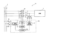
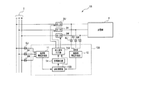
- FIG. 1 is a configuration diagram showing a configuration of a power system 1 to which an overvoltage suppressing device 10 according to a first embodiment of the present invention is applied.
- symbol is attached
- the power system 1 includes a power bus 2, a three-phase circuit breaker 3U, 3V, 3W, a power transmission line 4, a three-phase power-side voltage detector 5U, 5V, 5W, and a three-phase line. Side voltage detectors 6U, 6V, 6W and an overvoltage suppression device 10 are provided.
- the power source bus 2 is a power system bus provided with a three-phase AC power source composed of a U phase, a V phase, and a W phase.
- the power transmission line 4 is electrically connected to the power bus 2 via the circuit breakers 3U, 3V, 3W. Although not shown, a reactor is installed between the ground of each phase of the transmission line 4. These reactors may be installed at both ends of the transmission line 4 or may be installed only at one end.
- Circuit breakers 3U, 3V, 3W connect the phases of power transmission line 4 and power supply bus 2 to each other.
- the circuit breakers 3U, 3V, 3W are each phase operation type circuit breakers operated individually for each phase.
- the circuit breakers 3U, 3V, 3W are provided in the U phase, the V phase, and the W phase, respectively.
- Each power supply side voltage detector 5U, 5V, 5W is provided in each corresponding phase of the power supply bus 2.
- the power supply side voltage detectors 5U, 5V, 5W are, for example, instrument transformers.
- Each power supply side voltage detector 5U, 5V, 5W detects a corresponding phase voltage (ground voltage) of each power supply bus 2. That is, each power supply side voltage detector 5U, 5V, 5W detects the voltage of the power supply side of each corresponding circuit breaker 3U, 3V, 3W.
- Each power supply side voltage detector 5U, 5V, 5W outputs each detected phase voltage of the power supply bus 2 to the overvoltage suppressing device 10.
- Each line-side voltage detector 6U, 6V, 6W is provided in each corresponding phase of the transmission line 4.
- the line side voltage detectors 6U, 6V, 6W are, for example, instrument transformers.
- Each line-side voltage detector 6U, 6V, 6W detects a corresponding phase voltage (ground voltage) of the transmission line 4. That is, each line side voltage detector 6U, 6V, 6W detects the voltage on the line side of the circuit breakers 3U, 3V, 3W of the corresponding phases.
- Each line side voltage detector 6U, 6V, 6W outputs each detected phase voltage of the transmission line 4 to the overvoltage suppressing device 10.
- the overvoltage suppressing device 10 includes each phase voltage of the power source bus 2 detected by the power source side voltage detectors 5U, 5V, 5W and each phase voltage of the transmission line 4 detected by the line side voltage detectors 6U, 6V, 6W. Is entered. When the circuit breakers 3U, 3V, 3W are opened, the overvoltage suppressing device 10 turns on the circuit breakers 3U, 3V, 3W based on the phase voltages of the power supply bus 2 and the phase voltages of the power transmission line 4.
- the overvoltage suppression device 10 includes a power supply side voltage measurement unit 11, a line side voltage measurement unit 12, a waveform calculation unit 13, a phase detection unit 14, and a closing command output unit 15.
- the power source side voltage measuring unit 11 measures the power source side voltages of the circuit breakers 3U, 3V, 3W detected by the power source side voltage detectors 5U, 5V, 5W.
- the power supply side voltage measurement unit 11 outputs the measured voltage waveform data on the power supply side of the circuit breakers 3U, 3V, 3W to the waveform calculation unit 13.
- the line side voltage measuring unit 12 measures the voltage of the transmission line 4 detected by the line side voltage detectors 6U, 6V, 6W.
- the line side voltage measurement unit 12 outputs the measured voltage waveform data of the power transmission line 4 to the waveform calculation unit 13.
- the waveform calculation unit 13 applies the circuit breakers 3U and 3V to the voltage waveform data of the power supply bus 2 measured by the power supply side voltage measurement unit 11 and the voltage waveform data of the transmission line 4 measured by the line side voltage measurement unit 12. , Waveform calculation processing for detecting the phase (timing) at which 3 W is input is performed. The waveform calculation unit 13 outputs the voltage waveform data subjected to the waveform calculation process to the phase detection unit 14.
- the phase detection unit 14 detects the phase at which the circuit breakers 3U, 3V, and 3W are respectively turned on based on the voltage waveform data that has been subjected to waveform calculation processing by the waveform calculation unit 13.
- the phase detection unit 14 outputs the detected phase to be input for each phase to the input command output unit 15.
- the closing command output unit 15 outputs a closing command for turning on the circuit breakers 3U, 3V, and 3W at the phase of each phase detected by the phase detector 14.
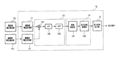
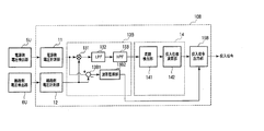
- FIG. 2 is a block diagram showing the configuration of the overvoltage suppressing device 10 according to the first embodiment of the present invention.
- FIG. 2 although the structure of only one phase among circuit breakers 3U, 3V, and 3W is illustrated, the other two phases shall be comprised similarly.
- the waveform calculation unit 13 includes a multiplier 131, a low-pass filter 132, and a high-pass filter 133.
- the multiplier 131 receives the voltage waveform data on the power supply side of the circuit breaker 3U measured by the power supply side voltage measurement unit 11 and the voltage waveform data on the line side of the circuit breaker 3U measured by the line side voltage measurement unit 12. The The multiplier 131 multiplies the voltage waveform data on the power source side of the circuit breaker 3U by the voltage waveform data on the line side of the circuit breaker 3U. The multiplier 131 outputs the voltage waveform data calculated by multiplication to the low-pass filter 132.
- the voltage waveform data calculated by the multiplier 131 is input to the low pass filter 132.
- the cutoff frequency of the low-pass filter 132 is set to a frequency that can cut the commercial frequency.
- the low-pass filter 132 allows only the frequency component lower than the cutoff frequency to pass through the input voltage waveform data. Thereby, the low pass filter 132 removes the commercial frequency component which is a high frequency component from the input voltage waveform data.
- the low pass filter 132 outputs the passed voltage waveform data to the high pass filter 133.
- the frequency of the voltage oscillation of the transmission line 4 after breaking the circuit breakers 3U, 3V, 3W varies depending on the compensation rate of the installed reactor, but is close to the commercial frequency that is the frequency of the power supply side voltage. For this reason, a component having a frequency lower than the commercial frequency appears in the voltage between the electrodes of the circuit breakers 3U, 3V, and 3W. Therefore, the cutoff frequency of the low-pass filter 133 is set to a frequency that can cut the commercial frequency.
- the voltage waveform data that has passed through the low pass filter 132 is input to the high pass filter 133.
- the cut-off frequency of the high-pass filter 133 is set to a frequency that can cut an extremely low frequency component close to a DC component.
- the high pass filter 133 allows only the frequency component higher than the cutoff frequency to pass through the input voltage waveform data. Thereby, the high-pass filter 133 removes an extremely low frequency component from the input voltage waveform data.
- the high pass filter 133 outputs the passed voltage waveform data to the period detection unit 141 of the phase detection unit 14.
- the phase detection unit 14 includes a period detection unit 141 and a closing phase calculation unit 142.
- the voltage waveform data that has passed through the high-pass filter 133 is input to the period detection unit 141.
- the cycle detection unit 141 calculates a cycle in which the voltage between the electrodes of the circuit breaker 3U is minimized based on the input voltage waveform data.
- the period detection unit 141 outputs the calculated period to the input phase calculation unit 142.
- the cycle calculated by the cycle detection unit 141 is input to the input phase calculation unit 142.
- the closing phase calculation unit 142 calculates the optimal time (phase) for closing the circuit breaker 3U based on the input cycle.
- the optimal closing time is a time when the voltage waveform of the inter-electrode voltage of the circuit breaker 3U is estimated to be minimized thereafter.
- the making phase calculation unit 142 outputs the calculated time to the making command output unit 15.
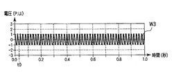
- FIGS. 3 to 8 are waveform diagrams showing voltage waveforms W3 to W8 for explaining the arithmetic processing in the overvoltage suppressing device 10 according to the present embodiment.
- FIGS. 3 to 8 show the respective voltage waveforms W3 to W8 from around time t0 when the circuit breaker 3U shuts off the power transmission line 4.
- FIG. 3 is a waveform diagram showing a voltage waveform W3 of the power source side voltage (voltage of the power source bus 2) of the circuit breaker 3U measured by the power source side voltage measuring unit 11.
- FIG. 4 is a waveform diagram showing a voltage waveform W4 of the line side voltage (voltage of the power transmission line 4) of the circuit breaker 3U measured by the line side voltage measurement unit 12.
- FIG. 5 is a waveform diagram showing a voltage waveform W5 of the interelectrode voltage of the circuit breaker 3U.
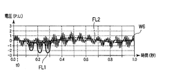
- FIG. 6 is a waveform diagram showing a voltage waveform W6 calculated by the multiplier 131. As shown in FIG. FIG. FIG.
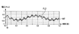
- FIG. 7 is a waveform diagram showing a voltage waveform W7 that has been arithmetically processed by the low-pass filter 132.
- FIG. 8 is a waveform diagram showing a voltage waveform W8 that is arithmetically processed by the high-pass filter 133. As shown in FIG.
- a voltage represented by a voltage waveform W3 shown in FIG. 3 is applied to the power supply side of the circuit breaker 3U.
- a voltage represented by a voltage waveform W4 shown in FIG. 4 is applied to the line side of the circuit breaker 3U.
- the voltage between the electrodes of the circuit breaker 3U is represented by a voltage waveform W5 shown in FIG.
- the voltage waveform W5 is obtained by subtracting the voltage waveform W4 on the line side of the circuit breaker 3U from the voltage waveform W3 on the power supply side of the circuit breaker 3U.
- the voltage waveform W5 is zero before the time t0 because the voltage on the power source side of the circuit breaker 3U and the voltage on the line side of the circuit breaker 3U are the same.
- the multiplier 131 receives the voltage waveform data on the power source side of the circuit breaker 3U indicating the voltage waveform W3 and the voltage waveform data on the line side of the circuit breaker 3U indicating the voltage waveform W4.
- the multiplier 131 multiplies the input two voltage waveform data. Thereby, the multiplier 131 calculates voltage waveform data indicating the voltage waveform W6 shown in FIG.
- a commercial frequency component that is a harmonic component, a low frequency component FL1, and a very low frequency component FL2 are superimposed on the voltage waveform W6.
- the low-pass filter 132 receives voltage waveform data indicating the voltage waveform W6 calculated by the multiplier 131. Thereby, the low pass filter 132 calculates voltage waveform data indicating the voltage waveform W7 shown in FIG.
- the voltage waveform W7 is a waveform in which the commercial frequency component is suppressed and the low frequency component FL1 and the extremely low frequency component FL2 are extracted from the voltage waveform W6.
- the voltage waveform data representing the voltage waveform W7 calculated by the low pass filter 132 is input to the high pass filter 133. Accordingly, the high pass filter 133 calculates voltage waveform data indicating the voltage waveform W8 shown in FIG.
- the voltage waveform W8 is a waveform in which the extremely low frequency component FL2 is suppressed with respect to the voltage waveform W7, and the low frequency component FL1 in the frequency band lower than the frequency of the power supply bus 2 and higher than the frequency of the DC component is extracted. ing.
- the period detector 141 receives voltage waveform data indicating the voltage waveform W8 that has been subjected to waveform calculation by the waveform calculator 13.
- the period detector 141 monitors the voltage waveform data indicating the voltage waveform W8 until a preset time elapses after the circuit breaker 3U blocks the power transmission line 4.
- the period detector 141 detects the time tc that is the maximum in the positive polarity in the monitored voltage waveform W8. By this detection, the cycle detection unit 141 measures the interval at which the time tc appears.
- the period detector 141 calculates the period TM based on the measured interval.
- the period detection unit 141 outputs the calculated period TM to the input phase calculation unit 142.
- the time tc at which the positive polarity in the voltage waveform W8 is maximized coincides with the time tc at which the voltage of the double frequency of the voltage waveform W5 is minimized. Therefore, the period TM calculated by the period detection unit 141 is the same as the period TM in which the multi-frequency voltage of the voltage waveform W5 of the interelectrode voltage is minimized.
- the closing phase calculation unit 142 calculates a closing phase (closing time) that is optimal for turning on the circuit breaker 3U based on the cycle TM calculated by the cycle detection unit 141.
- This input phase is one of the phases in which the voltage waveform W8 is estimated to be maximum at the positive polarity thereafter.
- the closing command output unit 15 outputs a closing command to the circuit breaker 3U so that the circuit breaker 3U is turned on at the closing phase calculated by the closing phase calculation unit 142.
- a low frequency component FL1 in a frequency band lower than the frequency of the power supply bus 2 and higher than the frequency of the DC component appears remarkably.
- FL1 is a multi-frequency component of the circuit breaker pole voltage W5.
- the low frequency component FL1 is extracted by the low pass filter 132 and the high pass filter 133.
- the time when the interpolar voltage of the circuit breakers 3U, 3V, 3W becomes small can be estimated by obtaining the period TM having the maximum positive polarity.
- the overvoltage suppressing device 10 turns on the circuit breaker 3U, 3V, 3W at an optimum time when the circuit voltage of the circuit breakers 3U, 3V, 3W becomes small, so that the voltage between the electrodes becomes double frequency. Even if it is, the overvoltage generated when the circuit breakers 3U, 3V, and 3W are turned on can be suppressed.
- FIG. 9 is a block diagram which shows the structure of 1 A of electric power grid systems with which the overvoltage suppression apparatus 10A which concerns on the 2nd Example of this invention was applied.
- Power system 1A has a configuration in which overvoltage suppression device 10A is provided in place of overvoltage suppression device 10 in power system 1 according to the first embodiment shown in FIG. In other respects, the power system 1A is the same as the power system 1 according to the first embodiment.
- FIG. 10 is a configuration diagram showing the configuration of the overvoltage suppressing device 10A according to the present embodiment.
- the overvoltage suppression device 10A has a configuration in which a waveform calculation unit 13A is provided instead of the waveform calculation unit 13 in the overvoltage suppression device 10 according to the first embodiment illustrated in FIG. In other respects, the overvoltage suppressing device 10A is the same as the overvoltage suppressing device 10 according to the first embodiment.
- the waveform calculation unit 13A includes a subtractor 13A1, a multiplier 13A2, a low-pass filter 13A3, and a high-pass filter 13A4.
- the voltage waveform data on the power source side of the circuit breaker 3U measured by the power source side voltage measuring unit 11 and the voltage waveform data on the line side of the circuit breaker 3U measured by the line side voltage measuring unit 12 are input to the subtractor 13A1.
- the subtractor 13A1 subtracts the voltage waveform data on the line side of the circuit breaker 3U from the voltage waveform data on the power supply side of the circuit breaker 3U. By this calculation, voltage waveform data of the voltage between the electrodes of the circuit breaker 3U is calculated.
- the subtractor 13A1 outputs the calculated voltage waveform data of the interelectrode voltage to the multiplier 13A2.
- the voltage waveform data of the interelectrode voltage calculated by the subtractor 13A1 is input to the multiplier 13A2.
- the multiplier 13A2 squares the input voltage waveform data.
- the multiplier 13A2 outputs the voltage waveform data calculated by squaring to the low-pass filter 13A3.
- the voltage waveform data squared by the multiplier 13A2 is input to the low-pass filter 13A3.
- the cut-off frequency of the low-pass filter 13A3 is set to a frequency that can cut the commercial frequency.
- the low-pass filter 13A3 allows only the frequency component lower than the cutoff frequency to pass through the input voltage waveform data. Thereby, the low pass filter 13A3 removes the commercial frequency component which is a high frequency component from the input voltage waveform data.
- the low pass filter 13A3 outputs the passed voltage waveform data to the high pass filter 13A4.
- the voltage waveform data that has passed through the low-pass filter 13A3 is input to the high-pass filter 13A4.
- the cut-off frequency of the high-pass filter 13A4 is set to a frequency that can cut a very low frequency component close to a direct current component.
- the high-pass filter 13A4 allows only the frequency component higher than the cutoff frequency to pass through the input voltage waveform data. Thereby, the high pass filter 13A4 removes an extremely low frequency component from the input voltage waveform data.
- the high pass filter 13A4 outputs the passed voltage waveform data to the period detection unit 141 of the phase detection unit 14.
- FIGS. 11 to 16 are waveform diagrams showing voltage waveforms for explaining the calculation processing in the overvoltage suppressing device 10A according to the present embodiment.
- 11 to 16 show the respective voltage waveforms W11 to W16 from around time t1 when the circuit breaker 3U shuts off the power transmission line 4.
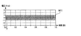
- FIG. 11 is a waveform diagram showing a voltage waveform W11 of the power supply side voltage (voltage of the power supply bus 2) of the circuit breaker 3U measured by the power supply side voltage measurement unit 11.
- FIG. 12 is a waveform diagram showing a voltage waveform W12 of the line side voltage (voltage of the power transmission line 4) of the circuit breaker 3U measured by the line side voltage measuring unit 12.
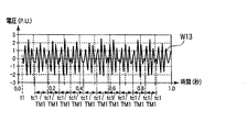
- FIG. 13 is a waveform diagram showing a voltage waveform W13 of the inter-electrode voltage of the circuit breaker 3U that has been subjected to arithmetic processing by the subtractor 13A1.
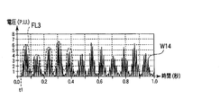
- FIG. 14 is a waveform diagram showing a voltage waveform W14 that has been arithmetically processed by the multiplier 13A2.
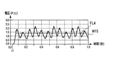
- FIG. 15 is a waveform diagram showing a voltage waveform W15 calculated by the low pass filter 13A3.
- FIG. 16 is a waveform diagram showing a voltage waveform W16 calculated by the high-pass filter 13A4.
- a voltage represented by a voltage waveform W11 shown in FIG. 11 is applied to the power supply side of the circuit breaker 3U.
- a voltage represented by a voltage waveform W12 shown in FIG. 12 is applied to the line side of the circuit breaker 3U.
- the voltage waveform data on the power source side of the circuit breaker 3U indicating the voltage waveform W11 and the voltage waveform data on the line side of the circuit breaker 3U indicating the voltage waveform W12 are input to the subtractor 13A1.
- the subtractor 13A1 subtracts the voltage waveform data on the line side of the circuit breaker 3U from the voltage waveform data on the power supply side of the circuit breaker 3U. Thereby, the subtractor 13A1 calculates the voltage waveform data of the voltage between the electrodes of the circuit breaker 3U indicating the voltage waveform W13 shown in FIG.
- the voltage waveform W13 is zero before the time t1, since the voltage on the power supply side of the circuit breaker 3U and the voltage on the line side of the circuit breaker 3U are the same.
- the voltage waveform data of the voltage between the electrodes of the circuit breaker 3U indicating the voltage waveform W13 calculated by the subtractor 13A1 is input to the multiplier 13A2.
- the multiplier 13A2 squares the input voltage waveform data. Thereby, the multiplier 13A2 calculates voltage waveform data indicating the voltage waveform W14 shown in FIG.
- a commercial frequency component that is a harmonic component, a low frequency component FL3, and an extremely low frequency component FL4 shown in FIG. 15 are superimposed.
- the voltage waveform data indicating the voltage waveform W14 calculated by the subtractor 13A2 is input to the low-pass filter 13A3.
- the low-pass filter 13A3 calculates voltage waveform data indicating the voltage waveform W15 shown in FIG.
- the voltage waveform W15 is a waveform in which the commercial frequency component is suppressed and the low frequency component FL3 and the extremely low frequency component FL4 are extracted from the voltage waveform W14.
- the voltage waveform data representing the voltage waveform W15 calculated by the low-pass filter 13A3 is input to the high-pass filter 13A4.
- the high-pass filter 13A4 calculates voltage waveform data indicating the voltage waveform W16 shown in FIG.
- the voltage waveform W16 is a waveform in which the extremely low frequency component FL4 is suppressed with respect to the voltage waveform W15, and the low frequency component FL3 in the frequency band lower than the frequency of the power supply bus 2 and higher than the frequency of the DC component is extracted. ing.
- the period detector 141 receives voltage waveform data indicating the voltage waveform W16 that has been waveform-calculated by the waveform calculator 13A.
- the period detector 141 monitors the voltage waveform data indicating the voltage waveform W16 until a preset time elapses after the circuit breaker 3U blocks the power transmission line 4.
- the period detection unit 141 detects a time tc1 that is negative and maximum in the monitored voltage waveform W16. By this detection, the period detection unit 141 measures an interval at which the time tc1 appears.
- the period detector 141 calculates the period TM1 based on the measured interval.
- the period detector 141 outputs the calculated period TM1 to the input phase calculator 142.
- the time tc1 at which the voltage waveform W16 has the maximum negative polarity coincides with the time tc1 at which the double frequency voltage of the voltage waveform W13 decreases. Therefore, the period TM1 calculated by the period detection unit 141 is the same as the period TM1 in which the multi-frequency voltage of the voltage waveform W13 of the interelectrode voltage decreases.
- the closing phase calculation unit 142 calculates a closing phase (closing time) optimum for turning on the circuit breaker 3U based on the cycle TM1 calculated by the cycle detection unit 141.
- This input phase is one of the phases in which the voltage waveform W16 is estimated to be negative and maximum in the future.
- the closing command output unit 15 outputs a closing command to the circuit breaker 3U so that the circuit breaker 3U is turned on at the closing phase calculated by the closing phase calculation unit 142.
- the overvoltage suppression device 10A turns on the circuit breaker 3U, 3V, 3W at the optimum time when the circuit voltage of the circuit breakers 3U, 3V, 3W becomes small, so that the voltage between the electrodes becomes double frequency. Even if it is, the overvoltage generated when the circuit breakers 3U, 3V, and 3W are turned on can be suppressed.
- the overvoltage suppressing device 10A the interpolar voltage is directly obtained, and this interpolar voltage is squared. Therefore, the difference in the voltage between the electrodes is more clearly defined than in the overvoltage suppressing device 10 according to the first embodiment. can do. Thereby, the overvoltage suppressing device 10A can perform control with higher accuracy than the overvoltage suppressing device 10 according to the first embodiment.
- the overvoltage suppression device 10A instead of the calculation in the multiplier 131 in the overvoltage suppression device 10 according to the first embodiment, the calculation by the subtractor A1 and the multiplier 13A2 is necessary. For this reason, the overvoltage suppression device 10 according to the first embodiment is faster in calculation speed than the overvoltage suppression device 10A.
- FIG. 17 is a block diagram which shows the structure of the electric power grid
- the electric power system 1B is the structure which provided the overvoltage suppression apparatus 10B instead of the overvoltage suppression apparatus 10 in the electric power system 1 which concerns on the 1st Example shown in FIG. About other points, electric power system 1B is the same as electric power system 1 concerning a 1st example.
- FIG. 18 is a configuration diagram showing the configuration of the overvoltage suppressing device 10B according to the present embodiment.
- the overvoltage suppressing device 10 ⁇ / b> B is provided with a waveform calculating unit 13 ⁇ / b> B instead of the waveform calculating unit 13, and a closing command output unit 15 ⁇ / b> B instead of the closing command output unit 15. Is provided.
- the overvoltage suppressing device 10B is the same as the overvoltage suppressing device 10 according to the first embodiment.
- the waveform calculation unit 13B has a configuration in which a subtractor 13B1 and a waveform monitoring unit 13B2 are added to the waveform calculation unit 13 according to the first embodiment.
- the voltage waveform data on the power source side of the circuit breaker 3U measured by the power source side voltage measuring unit 11 and the voltage waveform data on the line side of the circuit breaker 3U measured by the line side voltage measuring unit 12 are input to the subtractor 13B1.
- the subtractor 13B1 subtracts the voltage waveform data on the line side of the circuit breaker 3U from the voltage waveform data on the power supply side of the circuit breaker 3U. By this calculation, voltage waveform data of the voltage between the electrodes of the circuit breaker 3U is calculated.
- the subtractor 13B1 outputs the voltage waveform data of the calculated interelectrode voltage to the waveform monitoring unit 13B2.
- the voltage waveform data of the interelectrode voltage calculated by the subtractor 13B1 is input to the waveform monitoring unit 13B2.
- the secondary arc current that flows on the line side (transmission line 4) of the circuit breaker 3U is preset based on the voltage waveform data of the interelectrode voltage after the transmission line 4 is interrupted by the circuit breaker 3U. It is monitored whether or not the arc is extinguished within a set time (for example, 100 milliseconds).
- the judgment method of extinction of the secondary arc current by the waveform monitoring unit 13B2 is performed by detecting that the waveform of the interelectrode voltage has changed. For example, as a method of detecting a change in the waveform of the interelectrode voltage, there is a method of determining based on the frequency of the interelectrode voltage. While the secondary arc current is not extinguished, the voltage on the line side of the circuit breaker 3U is zero. For this reason, the voltage between the electrodes becomes the same as the voltage (for example, commercial frequency) on the power source side of the circuit breaker 3U.
- the waveform monitoring unit 13B2 can detect that the secondary arc current has been extinguished by detecting that the frequency of the interelectrode voltage has decreased.
- the waveform monitoring unit 13B2 ends the calculation process when the secondary arc current is extinguished within the set time.
- the waveform monitoring unit 13B2 does not perform waveform processing by calculation by the multiplier 131 or the like based on the voltage waveform data of the interelectrode voltage, and performs a surge surge ( Overvoltage) is suppressed, and arithmetic processing for turning on the circuit breaker 3U is performed.
- the waveform monitoring unit 13B2 outputs to the input command output unit 15B based on the calculation result.
- the circuit breaker in the case of a high-speed reclosing circuit, the circuit breaker has a duty of breaking- ⁇ -turning-on / breaking- (1 minute) -turning-on / breaking.
- ⁇ is 0.35 seconds as a standard.
- the time until the secondary arc current is extinguished after the circuit breaker 3U is opened depends on weather conditions and is not constant. Therefore, if the arc extinguishing time of the secondary arc current is delayed, it may be difficult to estimate by the waveform processing the time when the interelectrode voltage decreases within the time ⁇ of the high-speed reclosing circuit.
- the waveform monitoring unit 13B2 opens the circuit breaker 3U within the time when the circuit breaker 3U can be turned on within the time ⁇ even if the time when the voltage between the electrodes is reduced is estimated by waveform processing.
- the maximum time that can be spent until the secondary arc current is extinguished is set as the set time. That is, when it takes a long time for the secondary arc current to extinguish for longer than this set time, the overvoltage suppression device 10B performs waveform processing to estimate the time when the interelectrode voltage decreases, This means that the unit 3U cannot be re-inserted within the time ⁇ required for the above-mentioned operation responsibility.
- the overvoltage suppressing device 10B performs waveform processing to estimate a point in time when the interelectrode voltage becomes small.
- the overvoltage suppressing device 10B turns on the circuit breaker 3U at the turning-on time calculated by the waveform monitoring unit 13B2.
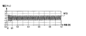
- FIGS. 19 to 21 are waveform diagrams showing voltage waveforms for explaining the calculation processing in the overvoltage suppressing device 10B according to the present embodiment.
- FIGS. 19 to 21 show states of voltage waveforms W19 to W21 from around time t2 when the circuit breaker 3U shuts off the power transmission line 4, respectively.
- the vertical axis represents voltage (p.u.) and the horizontal axis represents time (seconds).
- FIG. 19 is a waveform diagram showing a voltage waveform W19 of the power source side voltage (voltage of the power source bus 2) of the circuit breaker 3U measured by the power source side voltage measuring unit 11.
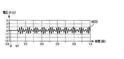
- FIG. 20 is a waveform diagram showing a voltage waveform W20 of the line side voltage (voltage of the power transmission line 4) of the circuit breaker 3U measured by the line side voltage measurement unit 12.
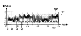
- FIG. 21 is a waveform diagram showing a voltage waveform W21 of the inter-electrode voltage of the circuit breaker 3U that has been subjected to arithmetic processing by the subtractor 13B1.
- a voltage represented by a voltage waveform W19 shown in FIG. 19 is applied to the power supply side of the circuit breaker 3U.
- a voltage represented by a voltage waveform W20 shown in FIG. 20 is applied to the line side of the circuit breaker 3U.
- the transmission line U phase is in a 1-wire ground fault condition. For this reason, the voltage side voltage W19 and the line side voltage W20 are zero before time t2 in FIGS. Since the circuit breaker 3U is cut off at time t2, the power supply voltage W19 appears as the power supply voltage thereafter. On the other hand, the failure of the power transmission line 4 continues until time t21. That is, the secondary arc voltage continues until time t21. Time t21 indicates a point in time when the secondary arc current is extinguished. Accordingly, the voltage waveform W20 representing the voltage of the transmission line 4 is zero until time t21.
- the voltage waveform data on the power supply side of the circuit breaker 3U indicating the voltage waveform W19 and the voltage waveform data on the line side of the circuit breaker 3U indicating the voltage waveform W20 are input to the subtractor 13B1.
- the subtractor 13B1 subtracts the voltage waveform data on the line side of the circuit breaker 3U from the voltage waveform data on the power supply side of the circuit breaker 3U. Thereby, subtractor 13B1 calculates the voltage waveform data of the voltage between electrodes of circuit breaker 3U which shows voltage waveform W21 shown in FIG.
- the voltage waveform W21 is zero before the time t2, since the voltage on the power source side of the circuit breaker 3U and the voltage on the line side of the circuit breaker 3U are the same.
- the waveform monitoring unit 13B2 receives the voltage waveform data of the voltage across the circuit breaker 3U indicating the voltage waveform W21 calculated by the subtractor 13B1 and the voltage waveform data on the line side of the circuit breaker 3U indicating the voltage waveform W20. .
- the waveform monitoring unit 13B2 measures the time from time t2 when the circuit breaker 3U is opened to time t21 when the secondary arc current is extinguished.
- the waveform monitoring unit 13B2 ends the calculation process when the time from the time t2 when the circuit breaker 3U is opened to the time t21 when the secondary arc current is extinguished is shorter than the set time.
- the waveform monitoring unit 13B2 displays the voltage across the circuit breaker 3U indicating the voltage waveform W21.
- a time point at which the voltage waveform data has a voltage value lower than preset voltage thresholds THP and THN (here, ⁇ 1.5 p.u.) is detected. Based on this detection result, the waveform monitoring unit 13B2 determines that the inter-pole voltage of the circuit breaker 3U is 1.5 p. u. In the following, a closing command is output to the charging command output unit 15B so that the circuit breaker 3U is switched on.
- FIG. 22 is a waveform diagram schematically illustrating a closing surge VS generated when the circuit breaker inserts a no-load transmission line.
- FIG. 22 shows that the circuit breaker is turned on at time t3 and 3p. u. This shows a state in which a surge (overvoltage) VS is generated.
- the power supply voltage VP has a peak value of 1p. u. Is a sine wave.
- the DC voltage VL remaining on the transmission line before the circuit breaker is turned on again is 1 p. u. It is. 3p. u.
- the inter-electrode voltage (the difference between the instantaneous value of the power supply voltage VP and the DC voltage VL) at the time t3 when the input surge VS occurs is 2p. u. It is. That is, the input surge VS is about 1.5 times the voltage between the electrodes.
- the waveform monitoring unit 13B2 has an interelectrode voltage of 2p. u.
- the overvoltage due to the applied surge is reduced by 3p. u. Control lower than.
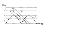
- FIG. 23 is a characteristic diagram showing pre-arc generation voltage characteristics VT0, VT1, and VT2 when the circuit breaker 3U according to the present embodiment is turned on.
- the interelectrode voltage VD is shown as an absolute value.
- the peak value of the interelectrode voltage VD is 1.5 p. u. It is said.
- the pre-arc generation voltage characteristic VT0 indicates a pre-arc generation voltage characteristic that is a standard for the circuit breaker 3U. Moreover, the circuit breaker generally has an operation variation and a discharge variation.
- the pre-arc generation voltage characteristics VT1 and VT2 indicate the pre-arc generation voltage characteristics in consideration of the operation variation and the discharge variation of the circuit breaker 3U with the pre-arc generation voltage characteristic VT0 as a reference.
- the circuit breaker 3U If the circuit breaker 3U is turned on so that the pre-arc generation voltage characteristic VT2 considering variation does not contact the inter-electrode voltage VD, the intersection of the pre-arc generation voltage characteristic VT1 and inter-electrode voltage VD considering the other variation is About 1 p. u. It is. Therefore, even when the variation of the circuit breaker 3U is taken into consideration, in FIG. u.
- the circuit breaker 3U can be turned on within.
- Pre-arc generation voltage characteristics, operation variation, and discharge variation vary depending on the circuit breaker. That is, the slopes of the pre-arc generation voltage characteristics VT0, VT1, and VT2 as shown in FIG.
- the pre-arcing voltage characteristics are straight to the right with respect to time, regardless of individual circuit breaker differences. That is, in any circuit breaker, the voltage at which the insulation between the breaker poles breaks down in proportion to the passage of time, that is, as the distance between the contacts decreases. Therefore, the inter-electrode voltage of the circuit breaker is 1.5 p. u.
- the circuit breaker 3U must be 1.5p. u.
- the circuit breaker 3U can be turned on at the following interelectrode voltage.
- the waveform monitoring unit 13B2 is capable of generating an instantaneous voltage of 1.5p. u.
- the phase at which the circuit breaker 3U is inserted as described below can be estimated by arithmetic processing. Therefore, when it takes time for the secondary arc current to extinguish for longer than the set time, the waveform monitoring unit 13B2 considers the pre-arc generation voltage characteristics VT0, VT1, VT2 of the circuit breaker 3U, and determines the voltage between the electrodes. 1.5 p. u.
- the circuit breaker 3U is inserted at the following timing. As a result, the circuit breaker 3U has a maximum overvoltage of 3p. u. It is suppressed smaller than.
- the overvoltage suppressing device 10B is provided with a waveform monitoring unit 13B2, and monitors each of the circuit breakers 3U, 3V, 3W until the secondary arc current is extinguished after being interrupted. When the secondary arc current is not extinguished within the set time, the overvoltage suppressing device 10B turns on the circuit breakers 3U, 3V, and 3W at the time of suppressing the overvoltage to some extent without performing the waveform processing by the multiplier 131 or the like. .
- the overvoltage suppression device 10B calculates the phase at which the circuit breakers 3U, 3V, and 3W are turned on without performing the waveform processing, so the circuit breakers 3U, 3V, and 3W are turned on in a shorter time than when the waveform processing is performed. Can be thrown in.
- the overvoltage suppression device 10B delays the time during which the secondary arc current is extinguished, and even if it is unable to perform the operation duty if the waveform processing by the multiplier 131 or the like is performed to calculate the input phase,
- the waveform monitoring unit 13B2 can turn on the circuit breakers 3U, 3V, and 3W while suppressing the overvoltage due to the closing surge within the time when the operation duty can be fulfilled.
- FIG. 24 is a configuration diagram showing a configuration of a power system 1C to which the overvoltage suppressing device 10C according to the fourth example of the present invention is applied.
- the power system 1C of electric power systems are the structures which provided the overvoltage suppression apparatus 10C instead of the overvoltage suppression apparatus 10 in the electric power system 1 which concerns on the 1st Example shown in FIG.
- the power system 1C is the same as the power system 1 according to the first embodiment.
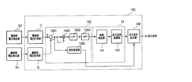
- FIG. 25 is a configuration diagram showing the configuration of the overvoltage suppressing device 10C according to the present embodiment.
- the overvoltage suppression device 10C has a configuration in which a waveform calculation unit 13C is provided instead of the waveform calculation unit 13B in the overvoltage suppression device 10B according to the third embodiment illustrated in FIG. In other respects, the overvoltage suppressing device 10C is the same as the overvoltage suppressing device 10B according to the third embodiment.
- the waveform calculation unit 13C is configured by adding a waveform monitoring unit 13B2 according to the third embodiment shown in FIG. 18 to the waveform calculation unit 13A according to the second embodiment shown in FIG. Voltage waveform data of the voltage between the electrodes calculated by the subtractor 13A1 is input to the waveform monitoring unit 13B2. In other respects, the waveform calculation unit 13C is the same as the waveform calculation unit 13A according to the second embodiment.
- the overvoltage suppression device 10C is provided with a waveform monitoring unit 13B2, and monitors each of the circuit breakers 3U, 3V, 3W until the secondary arc current is extinguished after being interrupted. When the secondary arc current is not extinguished within the set time, the overvoltage suppressing device 10C turns on the circuit breakers 3U, 3V, and 3W at the time of suppressing the overvoltage to some extent without performing the waveform processing by the multiplier 13A2. .
- the overvoltage suppression device 10C calculates the phase at which the circuit breakers 3U, 3V, and 3W are turned on without performing the waveform processing, so that the circuit breakers 3U, 3V, and 3W are installed in a shorter time than when the waveform processing is performed. Can be thrown in.
- the overvoltage suppressing device 10C delays the time during which the secondary arc current is extinguished, and even if the operation phase cannot be fulfilled by calculating the input phase by performing waveform processing using the multiplier 13A2, etc.
- the waveform monitoring unit 13B2 can turn on the circuit breakers 3U, 3V, and 3W while suppressing the overvoltage due to the closing surge within the time when the operation duty can be fulfilled.
- the low-pass filter and the high-pass filter are used.
- a band-pass filter may be used instead of these filters.
- the bandpass filter can transmit only a specific frequency band.
- the band pass filter can be set to transmit a frequency band that is not cut by the respective cutoff frequencies of the low pass filter and the high pass filter. That is, the band pass filter can be set to transmit only a predetermined frequency band lower than the commercial frequency (power supply frequency) and higher than the low frequency corresponding to the DC component.
- the components used in each embodiment may be software, hardware, or a combination of these.
- the various filters may be analog filters or digital filters.
- various arithmetic units such as a subtractor may have a hardware configuration (including calculation based on connection of wiring for taking in a voltage) or a configuration in which digital data is calculated by a computer.
- each embodiment it is possible to deal with an algorithm for calculating the maximum value and the minimum value of the waveform without providing a high-pass filter. For example, if low frequency components FL1 and FL3 in a frequency band lower than the frequency of the power supply bus 2 and higher than the frequency of the DC component appear to some extent clearly, the low frequency components FL1 and FL1 are detected by an algorithm without removing the DC components.
- the maximum value or the minimum value of FL3 may be obtained. That is, as long as the maximum and minimum values of the low frequency components FL1 and FL3 can be obtained substantially, this is the same as the extraction of the low frequency components FL1 and FL3.
- the configuration can be changed as appropriate depending on the performance of the calculation speed of the computer used for the overvoltage suppression device and the balance with the operation responsibilities of the circuit breaker.
- the voltage waveform data of the interelectrode voltage is squared, but any number may be used as long as it is an even number of 2 or more. That is, if the power is 2 ⁇ n (n is a natural number), the value raised to the nth power is squared, and as a result, the power is still squared.
- the determination of extinction of the secondary arc current flowing on the line side (transmission line 4) of the circuit breaker 3U is not limited to the embodiment.
- the determination of extinction of the secondary arc current may be based on other factors (phase or voltage value, etc.) instead of the frequency of the interelectrode voltage, or may not be determined based on the interelectrode voltage.
- the power transmission line 4 may be provided with a direct current detector or a direct current voltage detector to detect the secondary arc current.
- the present invention is not limited to the above-described embodiments as they are, and can be embodied by modifying the components without departing from the scope of the invention in the implementation stage.
- Various inventions can be formed by appropriately combining a plurality of constituent elements disclosed in the above embodiments. For example, some components may be deleted from all the components shown in the embodiments. Furthermore, constituent elements over different embodiments may be appropriately combined.
- the present invention is used in a power system and a distribution system using a circuit breaker.
- SYMBOLS 1 ... Power system system, 2 ... Power supply bus, 3U, 3V, 3W ... Circuit breaker for three phases, 4 ... Power transmission line, 5U, 5V, 5W ... Power supply side voltage detector for three phases, 6U, 6V, 6W ... Line-side voltage detectors for three phases, 10 ... overvoltage suppression device, 11 ... power supply-side voltage measurement unit, 12 ... line-side voltage measurement unit, 13 ... waveform calculation unit, 14 ... phase detection unit, 15 ... input command output Department.
Landscapes
- Engineering & Computer Science (AREA)
- Power Engineering (AREA)
- Keying Circuit Devices (AREA)
- Driving Mechanisms And Operating Circuits Of Arc-Extinguishing High-Tension Switches (AREA)
Abstract
Description
電源を備えた電力系統と送電線との接続を開閉する遮断器を開放後、前述の遮断器を投入する際に発生する過電圧を抑制する過電圧抑制装置であって、
前述の遮断器の前述の電力系統側の対地電圧である電源側電圧の波形を計測する電源側電圧計測手段と、
前述の遮断器の前述の送電線側の対地電圧である送電線側電圧の波形を計測する送電線側電圧計測手段と、
前述の電源側電圧計測手段により計測された前述の電源側電圧の波形と送電線側電圧計測手段により計測された前述の送電線側電圧の波形とを乗算した波形を演算する乗算手段と、
前述の乗算手段により演算された前述の波形から前述の電源の周波数よりも低く直流成分の周波数よりも高い周波数帯の成分の波形を抽出する抽出手段と、
前述の抽出手段により抽出された前述の波形が最大となる周期を検出する周期検出手段と、
前述の周期検出手段により検出された前述の周期に基づいて、前述の遮断器を投入する投入手段とを備えている。
図1は、本発明の第1の実施例に係る過電圧抑制装置10の適用された電力系統システム1の構成を示す構成図である。なお、以降の図における同一部分には同一符号を付してその詳しい説明を省略し、異なる部分について主に述べる。以降の実施例も同様にして重複する説明を省略する。
図9は、本発明の第2の実施例に係る過電圧抑制装置10Aの適用された電力系統システム1Aの構成を示す構成図である。
図17は、本発明の第3の実施例に係る過電圧抑制装置10Bの適用された電力系統システム1Bの構成を示す構成図である。
図24は、本発明の第4の実施例に係る過電圧抑制装置10Cの適用された電力系統システム1Cの構成を示す構成図である。
Claims (12)
- 電源を備えた電力系統と送電線との接続を開閉する遮断器を開放後、前記遮断器を投入する際に発生する過電圧を抑制する過電圧抑制装置であって、
前記遮断器の前記電力系統側の対地電圧である電源側電圧の波形を計測する電源側電圧計測手段と、
前記遮断器の前記送電線側の対地電圧である送電線側電圧の波形を計測する送電線側電圧計測手段と、
前記電源側電圧計測手段により計測された前記電源側電圧の波形と送電線側電圧計測手段により計測された前記送電線側電圧の波形とを乗算した波形を演算する乗算手段と、
前記乗算手段により演算された前記波形から前記電源の周波数よりも低く直流成分の周波数よりも高い周波数帯の成分の波形を抽出する抽出手段と、
前記抽出手段により抽出された前記波形が最大となる周期を検出する周期検出手段と、
前記周期検出手段により検出された前記周期に基づいて、前記遮断器を投入する投入手段と
を備えたことを特徴とする過電圧抑制装置。
- 前記送電線に流れる2次アーク電流が所定時間内に消弧したか否かを判断する消弧判断手段と、
前記電源側電圧計測手段により計測された前記電源側電圧の波形と送電線側電圧計測手段により計測された前記送電線側電圧の波形との差分である前記遮断器の極間電圧の波形を演算する極間電圧演算手段と、
前記消弧判断手段により前記所定時間内に前記2次アーク電流が消弧しなかったと判断された場合、前記極間電圧演算手段により演算された前記極間電圧の波形に基づいて、前記極間電圧の瞬時値の絶対値が閾値より低い電圧値となる前記遮断器を投入するための時点を推定する遮断器投入時点推定手段と、
前記遮断器投入時点推定手段により推定された前記時点で、前記遮断器を投入する短時間投入手段と
を備えたことを特徴とする請求項1に記載の過電圧抑制装置。
- 電源を備えた電力系統と送電線との接続を開閉する遮断器を開放後、前記遮断器を投入する際に発生する過電圧を抑制する過電圧抑制装置であって、
前記遮断器の前記電力系統側の対地電圧である電源側電圧の波形を計測する電源側電圧計測手段と、
前記遮断器の前記送電線側の対地電圧である送電線側電圧の波形を計測する送電線側電圧計測手段と、
前記電源側電圧計測手段により計測された前記電源側電圧の波形と送電線側電圧計測手段により計測された前記送電線側電圧の波形との差分である前記遮断器の極間電圧の波形を演算する極間電圧演算手段と、
前記極間電圧演算手段により演算された前記極間電圧の波形を2乗した波形を演算する2乗演算手段と、
前記2乗演算手段により演算された前記波形から前記電源の周波数よりも低く直流成分の周波数よりも高い周波数帯の成分の波形を抽出する抽出手段と、
前記抽出手段により抽出された前記波形が最小となる周期を検出する周期検出手段と、
前記周期検出手段により検出された前記周期に基づいて、前記遮断器を投入する投入手段と
を備えたことを特徴とする過電圧抑制装置。
- 前記送電線に流れる2次アーク電流が所定時間内に消弧したか否かを判断する消弧判断手段と、
前記消弧判断手段により前記所定時間内に前記2次アーク電流が消弧しなかったと判断された場合、前記極間電圧演算手段により演算された前記極間電圧の波形に基づいて、前記極間電圧の瞬時値の絶対値が閾値値より低い電圧値となる前記遮断器を投入するための時点を推定する遮断器投入時点推定手段と、
前記遮断器投入時点推定手段により推定された前記時点で、前記遮断器を投入する短時間投入手段と
を備えたことを特徴とする請求項3に記載の過電圧抑制装置。
- 前記抽出手段は、
低周波成分を抽出するローパスフィルタと、
高周波成分を抽出するハイパスフィルタとを備えたこと
を特徴とする請求項1から請求項4のいずれか1項に記載の過電圧抑制装置。
- 前記抽出手段は、所定の周波数帯を抽出するバンドパスフィルタであること
を特徴とする請求項1から請求項4のいずれか1項に記載の過電圧抑制装置。
- 電源を備えた電力系統と送電線との接続を開閉する遮断器を開放後、前記遮断器を投入する際に発生する過電圧を抑制する過電圧抑制方法であって、
前記遮断器の前記電力系統側の対地電圧である電源側電圧の波形を計測するステップと、
前記遮断器の前記送電線側の対地電圧である送電線側電圧の波形を計測するステップと、
前記電源側電圧の波形と前記送電線側電圧の波形とを乗算した波形を演算するステップと、
前記乗算した波形から前記電源の周波数よりも低く直流成分の周波数よりも高い周波数帯の成分の波形を抽出するステップと、
抽出された前記波形が最大となる周期を検出するステップと、
前記周期に基づいて、前記遮断器を投入するステップと
を含むことを特徴とする過電圧抑制方法。
- 前記送電線に流れる2次アーク電流が所定時間内に消弧したか否かを判断するステップと、
前記電源側電圧の波形と前記送電線側電圧の波形との差分である前記遮断器の極間電圧の波形を演算するステップと、
前記所定時間内に前記2次アーク電流が消弧しなかったと判断された場合、前記極間電圧の波形に基づいて、前記極間電圧の瞬時値の絶対値が閾値より低い電圧値となる前記遮断器を投入するための時点を推定するステップと、
前記時点で、前記遮断器を投入するステップと
を含むことを特徴とする請求項7に記載の過電圧抑制方法。
- 電源を備えた電力系統と送電線との接続を開閉する遮断器を開放後、前記遮断器を投入する際に発生する過電圧を抑制する過電圧抑制方法であって、
前記遮断器の前記電力系統側の対地電圧である電源側電圧の波形を計測するステップと、
前記遮断器の前記送電線側の対地電圧である送電線側電圧の波形を計測するステップと、
前記電源側電圧の波形と前記送電線側電圧の波形との差分である前記遮断器の極間電圧の波形を演算するステップと、
前記極間電圧の波形を2乗した波形を演算するステップと、
前記2乗した波形から前記電源の周波数よりも低く直流成分の周波数よりも高い周波数帯の成分の波形を抽出するステップと、
抽出された前記波形が最小となる周期を検出するステップと、
前記周期に基づいて、前記遮断器を投入するステップと
を含むことを特徴とする過電圧抑制方法。
- 前記送電線に流れる2次アーク電流が所定時間内に消弧したか否かを判断するステップと、
前記所定時間内に前記2次アーク電流が消弧しなかったと判断された場合、前記極間電圧の波形に基づいて、前記極間電圧の瞬時値の絶対値が閾値より低い電圧値となる前記遮断器を投入するための時点を推定するステップと、
前記時点で、前記遮断器を投入するステップと
を含むことを特徴とする請求項9に記載の過電圧抑制方法。
- 前記抽出するステップは、低周波成分を抽出するローパスフィルタ及び高周波成分を抽出するハイパスフィルタを用いて抽出すること
を特徴とする請求項7から請求項10のいずれか1項に記載の過電圧抑制方法。
- 前記抽出するステップは、所定の周波数帯を抽出するバンドパスフィルタを用いて抽出すること
を特徴とする請求項7から請求項10のいずれか1項に記載の過電圧抑制方法。
Priority Applications (3)
| Application Number | Priority Date | Filing Date | Title |
|---|---|---|---|
| CN201080002731XA CN102165551B (zh) | 2009-03-13 | 2010-03-01 | 过电压抑制装置 |
| US13/125,913 US8680713B2 (en) | 2009-03-13 | 2010-03-01 | Over-voltage suppression apparatus |
| CA 2738677 CA2738677C (en) | 2009-03-13 | 2010-03-01 | Over-voltage suppression apparatus |
Applications Claiming Priority (2)
| Application Number | Priority Date | Filing Date | Title |
|---|---|---|---|
| JP2009060925A JP5135266B2 (ja) | 2009-03-13 | 2009-03-13 | 過電圧抑制装置 |
| JP2009-060925 | 2009-03-13 |
Publications (1)
| Publication Number | Publication Date |
|---|---|
| WO2010103741A1 true WO2010103741A1 (ja) | 2010-09-16 |
Family
ID=42728040
Family Applications (1)
| Application Number | Title | Priority Date | Filing Date |
|---|---|---|---|
| PCT/JP2010/001371 Ceased WO2010103741A1 (ja) | 2009-03-13 | 2010-03-01 | 過電圧抑制装置 |
Country Status (5)
| Country | Link |
|---|---|
| US (1) | US8680713B2 (ja) |
| JP (1) | JP5135266B2 (ja) |
| CN (1) | CN102165551B (ja) |
| CA (1) | CA2738677C (ja) |
| WO (1) | WO2010103741A1 (ja) |
Cited By (1)
| Publication number | Priority date | Publication date | Assignee | Title |
|---|---|---|---|---|
| JP2012231627A (ja) * | 2011-04-27 | 2012-11-22 | Toyo Electric Mfg Co Ltd | 電力変換装置用遮断器のアーク防止方法 |
Families Citing this family (4)
| Publication number | Priority date | Publication date | Assignee | Title |
|---|---|---|---|---|
| WO2015056289A1 (ja) * | 2013-10-15 | 2015-04-23 | 三菱電機株式会社 | 電力開閉制御装置および閉極制御方法 |
| US10938204B1 (en) * | 2018-01-09 | 2021-03-02 | Timothy A Carty | System and method for detecting and isolating an electromagnetic pulse for protection of a monitored infrastructure |
| CN109100620B (zh) * | 2018-06-08 | 2022-04-22 | 中国电力科学研究院有限公司 | 一种验证抑制导线对gis变电站vfto抑制效果的系统和方法 |
| CN112836345A (zh) * | 2021-01-07 | 2021-05-25 | 云南电网有限责任公司电力科学研究院 | 一种断路器投切电抗器过电压仿真方法 |
Citations (2)
| Publication number | Priority date | Publication date | Assignee | Title |
|---|---|---|---|---|
| WO2000004564A1 (fr) * | 1998-07-16 | 2000-01-27 | Mitsubishi Denki Kabushiki Kaisha | Appareil de commutation synchrone |
| WO2008065757A1 (fr) * | 2006-11-29 | 2008-06-05 | Kabushiki Kaisha Toshiba | Appareil et procédé permettant de compresser un courant d'appel d'excitation d'un transformateur |
Family Cites Families (3)
| Publication number | Priority date | Publication date | Assignee | Title |
|---|---|---|---|---|
| JP5159075B2 (ja) * | 2006-09-25 | 2013-03-06 | 株式会社東芝 | 遮断器の開閉制御装置 |
| JP5259069B2 (ja) * | 2006-10-02 | 2013-08-07 | 株式会社東芝 | 遮断器の開閉制御システム |
| JP5248269B2 (ja) * | 2008-10-31 | 2013-07-31 | 株式会社東芝 | 遮断器の開閉制御装置、及び遮断器の開閉制御システム |
-
2009
- 2009-03-13 JP JP2009060925A patent/JP5135266B2/ja not_active Expired - Fee Related
-
2010
- 2010-03-01 CA CA 2738677 patent/CA2738677C/en active Active
- 2010-03-01 CN CN201080002731XA patent/CN102165551B/zh not_active Expired - Fee Related
- 2010-03-01 WO PCT/JP2010/001371 patent/WO2010103741A1/ja not_active Ceased
- 2010-03-01 US US13/125,913 patent/US8680713B2/en not_active Expired - Fee Related
Patent Citations (2)
| Publication number | Priority date | Publication date | Assignee | Title |
|---|---|---|---|---|
| WO2000004564A1 (fr) * | 1998-07-16 | 2000-01-27 | Mitsubishi Denki Kabushiki Kaisha | Appareil de commutation synchrone |
| WO2008065757A1 (fr) * | 2006-11-29 | 2008-06-05 | Kabushiki Kaisha Toshiba | Appareil et procédé permettant de compresser un courant d'appel d'excitation d'un transformateur |
Cited By (1)
| Publication number | Priority date | Publication date | Assignee | Title |
|---|---|---|---|---|
| JP2012231627A (ja) * | 2011-04-27 | 2012-11-22 | Toyo Electric Mfg Co Ltd | 電力変換装置用遮断器のアーク防止方法 |
Also Published As
| Publication number | Publication date |
|---|---|
| CA2738677A1 (en) | 2010-09-16 |
| US8680713B2 (en) | 2014-03-25 |
| CN102165551A (zh) | 2011-08-24 |
| CN102165551B (zh) | 2013-12-25 |
| JP5135266B2 (ja) | 2013-02-06 |
| CA2738677C (en) | 2014-01-21 |
| US20110204727A1 (en) | 2011-08-25 |
| JP2010218727A (ja) | 2010-09-30 |
Similar Documents
| Publication | Publication Date | Title |
|---|---|---|
| JP5472912B2 (ja) | 過電圧抑制装置 | |
| CN107966633B (zh) | 一种供电系统的配电网单相接地故障线路快速判断方法及系统 | |
| CN102576999B (zh) | 用于多相接地故障断续器的系统和方法 | |
| CN107449999B (zh) | 干扰电弧识别单元 | |
| CN109417285B (zh) | 直流电气回路保护装置及电弧检测方法 | |
| JP2016213179A (ja) | 直流回路遮断器および使用方法 | |
| CN109451770B (zh) | 故障电弧识别单元 | |
| JPH07236224A (ja) | 電流変化を利用したアーク検出装置及びその方法 | |
| JP2000188044A (ja) | 位相制御開閉装置 | |
| JP5135266B2 (ja) | 過電圧抑制装置 | |
| JPWO2017221493A1 (ja) | 直流電気回路保護装置およびアーク検出方法 | |
| JP2012195234A (ja) | 突入電流抑制装置 | |
| Poltl et al. | A new algorithm enabling controlled short circuit interruption | |
| CN110535116B (zh) | 一种消弧柜及小电流接地系统 | |
| KR101490770B1 (ko) | 지락 검출 장치 | |
| JP5547013B2 (ja) | 突入電流抑制装置 | |
| CN109613422A (zh) | 一种用于抑制潜供电流的断路器跳闸时刻控制方法 | |
| JP4717158B1 (ja) | 位相制御開閉装置 | |
| Liu et al. | Study on the influence of reignition on electrical life distribution of low-voltage circuit breakers | |
| CN210608530U (zh) | 一种消弧柜及小电流接地系统 | |
| CN113067410A (zh) | 一种交流滤波器断路器在线诊断分析系统及方法 | |
| CN106877307A (zh) | 软开关消弧装置 | |
| CN206559041U (zh) | 软开关消弧装置 | |
| Pavlyuchenko et al. | Controlled vacuum 6 (10) kV circuit breaker model | |
| CN112271693A (zh) | 工频首半波故障电流产生方法及暂态动稳定性检测方法 |
Legal Events
| Date | Code | Title | Description |
|---|---|---|---|
| WWE | Wipo information: entry into national phase |
Ref document number: 201080002731.X Country of ref document: CN |
|
| 121 | Ep: the epo has been informed by wipo that ep was designated in this application |
Ref document number: 10750500 Country of ref document: EP Kind code of ref document: A1 |
|
| WWE | Wipo information: entry into national phase |
Ref document number: 1977/DELNP/2011 Country of ref document: IN |
|
| WWE | Wipo information: entry into national phase |
Ref document number: 2738677 Country of ref document: CA |
|
| WWE | Wipo information: entry into national phase |
Ref document number: 13125913 Country of ref document: US |
|
| NENP | Non-entry into the national phase |
Ref country code: DE |
|
| 122 | Ep: pct application non-entry in european phase |
Ref document number: 10750500 Country of ref document: EP Kind code of ref document: A1 |