WO2010095657A1 - 放射線検出モジュール及び放射線撮像装置 - Google Patents
放射線検出モジュール及び放射線撮像装置 Download PDFInfo
- Publication number
- WO2010095657A1 WO2010095657A1 PCT/JP2010/052363 JP2010052363W WO2010095657A1 WO 2010095657 A1 WO2010095657 A1 WO 2010095657A1 JP 2010052363 W JP2010052363 W JP 2010052363W WO 2010095657 A1 WO2010095657 A1 WO 2010095657A1
- Authority
- WO
- WIPO (PCT)
- Prior art keywords
- radiation
- radiation detection
- support substrate
- detection module
- pixels
- Prior art date
- Legal status (The legal status is an assumption and is not a legal conclusion. Google has not performed a legal analysis and makes no representation as to the accuracy of the status listed.)
- Ceased
Links
Images

Classifications
-
- H—ELECTRICITY
- H10—SEMICONDUCTOR DEVICES; ELECTRIC SOLID-STATE DEVICES NOT OTHERWISE PROVIDED FOR
- H10F—INORGANIC SEMICONDUCTOR DEVICES SENSITIVE TO INFRARED RADIATION, LIGHT, ELECTROMAGNETIC RADIATION OF SHORTER WAVELENGTH OR CORPUSCULAR RADIATION
- H10F39/00—Integrated devices, or assemblies of multiple devices, comprising at least one element covered by group H10F30/00, e.g. radiation detectors comprising photodiode arrays
- H10F39/10—Integrated devices
- H10F39/12—Image sensors
- H10F39/18—Complementary metal-oxide-semiconductor [CMOS] image sensors; Photodiode array image sensors
- H10F39/189—X-ray, gamma-ray or corpuscular radiation imagers
Definitions
- the present invention relates to a radiation detection module and a radiation imaging apparatus, and more particularly to a technology capable of obtaining an image of high quality and facilitating assembly.
- one readout circuit is provided for one pixel element, and detection signals which are output upon incidence of radiation are individually read out to specify the incident position of the radiation.
- the upper limit of the integration degree of the readout circuit limits the increase in area of the radiation incident surface and the increase in pixel density.
- a double-sided silicon strip detector (DSSD) has been devised as a method of reading a large number of pixels with a small number of readout circuits.
- DSSD double-sided silicon strip detector
- a plurality of elongated electrodes are provided orthogonal to the upper and lower surfaces of the detector, and the incident position of the radiation is specified by reading out signals from both sides.
- N ⁇ M pixels by N + M readout circuits is established (see, for example, Non-Patent Document 1).
- the unit group of pixels needs to have a shape close to a square in order to obtain the reduction effect of the readout circuit. For this reason, when one of the unit clusters of the pixels breaks down, radiation can not be detected in the square area. In this case, it is difficult to complement data from surrounding pixel data, and a hole is formed in the image. Furthermore, in the technique of Non-Patent Document 1, it is necessary to increase the thickness of the detector in order to prevent penetration of the radiation and improve the detection efficiency, since the radiation is perpendicularly incident on the electrode surface of the detector. . However, when the thickness of the detector is increased, the mobility of the charge generated in the detector is reduced and the charge collection efficiency is reduced, so that the technique of Non-Patent Document 1 can not accurately measure the generated charge amount.
- Patent Document 1 discloses a technique in which radiation is incident in parallel to the electrode surface of a detection element in order to make two contradictory conditions regarding the thickness of the detector compatible. Further, in the technology of Patent Document 1, the signal wires drawn from the electrodes are connected on a separately provided substrate to reduce the number of read circuits using the same principle as that of the DSSD.
- An object of the present invention is to solve such problems, and to provide a radiation detection module that improves the image quality of an image and facilitates mounting and assembly of a radiation detection element, and a radiation imaging apparatus. Do.
- a plurality of first electrodes provided corresponding to one pixel are provided on one side of the semiconductor member, and a plurality of first electrodes are provided on the other side of the semiconductor member.
- a radiation detection element which outputs a detection signal to the first electrode and the second electrode when radiation is incident, and is erected along the incident direction of the radiation; Is detachably connected to a support substrate supporting a plurality of radiation detection elements arranged in orthogonal directions, and an external connection portion, and a bias voltage to the radiation detection elements is supplied from the connection portion, and a detection signal is transmitted to the connection portion And a connection portion for mechanically holding the support substrate against the connection portion, A plurality of first electrodes are connected on the support substrate, and the incident position of the radiation in the module is specified by simultaneously measuring detection signals from the first electrode and the second electrode.
- the number of signal lines drawn to the outside can be reduced, and the structure of the external connection portion and the connection portion for holding the support substrate in the connection portion can be simplified, and adjacent The intervals of the radiation detection modules can be narrowed.
- m radiation detection elements each having n pixels it is possible to reduce the number of reading wirings of detection signals to m + n while providing m ⁇ n pixels in one radiation detection module.
- the resistor and the capacitor are conventionally disposed on the outer side where the coupling portion is provided, the degree of integration of the wiring on the outer side is alleviated by moving to a vacant space of the support substrate.
- the portion where the high voltage is applied to the signal contact portion between the wires in the connection portion and the connection portion is reduced. Also, by making the unit group of pixels rectangular, it is possible to complement data from surrounding pixel data even if one of the pixels fails.
- a radiation detection module and a radiation imaging apparatus are provided that improve the image quality of the image and facilitate the mounting and maintenance of the detection element.
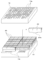
- FIG. 1 is an overall view showing a radiation imaging apparatus according to an embodiment of the present invention.
- FIG. 2 is an internal structural view of the radiation imaging apparatus according to the embodiment of the present invention.
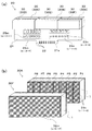
- FIG. 3A is a perspective view of a radiation detection module according to an embodiment of the present invention, and
- FIG. 3B is a radiation detection element applied to the radiation detection module.
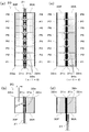
- Fig.4 (a) is a top view of the radiation detection module which concerns on embodiment, (b) is a side view, (c) is a top view which concerns on a modification, (d) is a deformation
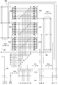
- FIG. 5 is a circuit diagram of the radiation detection module according to the embodiment.
- the radiation imaging apparatus 10 includes an imaging unit 15 in which a collimator 13 disposed to be a radiation incident surface is fixed to a frame 15 a, and data from the imaging unit 15 as a cable 12. And an image display unit 11 for collecting and displaying an image.
- the main configuration of the radiation imaging apparatus 10 described with reference to the later drawings is accommodated.
- a radioactive substance that generates gamma rays (radiation) having an energy of several tens of keV to several hundreds of keV is used for an imaging object of a gamma camera (radiographic imaging apparatus 10). Then, measurement is performed for each event of one radiation incident on the imaging unit 15, and an image obtained by the integration is displayed on the image display unit 11.
- the collimator 13 is made of a material having a high radiation shielding ability, such as lead, and provided with a large number of elongated hole openings 13a so that only radiation incident from a specific direction (the Z-axis direction in the drawing) passes.
- a radiation source not shown
- a planar image of the luminance distribution of the radiation is formed on the imaging unit 15.
- the luminance distribution of the radiation formed as a planar image is processed by the radiation detection module 20 (see FIG. 2) and the signal detection unit 14 inside the imaging unit 15, and information such as the radiation detection position and radiation detection energy It is sent to the image display unit 11 after being converted into digital data.
- the image display unit 11 creates an image using correction data and the like collected in advance based on the detected position and energy of the sent digital data, and displays the image on the screen.
- SPECT Single Photon Emission Computer Tomography
- the imaging unit 15 is rotated or arranged in multiple places around the subject who has administered the radioactive drug. Three-dimensional cross-sectional image information can be obtained.
- FIG. 2 shows the structure internally contained in the frame 15a (see FIG. 1).
- the internal structure is planarly arranged such that a plurality of radiation detection modules 20 for detecting incident radiation are parallel to the inside of the collimator 13.
- the plurality of radiation detection modules 20 can be detachably attached to the connection portion 14 c provided on the surface of the signal detection unit 14 at the connection portion 21 a.
- connection portion 21a mechanically holding the radiation detection module 20 in the external connection portion 14c
- the radiation detection module via the connection portion 14c is supplied with a bias voltage supplied from the signal detection portion 14 side. 20, and the detection signal that the radiation detection module 20 detects and outputs radiation is led to the signal detection unit 14 side via the connection unit 14c.
- the connection portion 21a obtains electrical conduction by mechanically contacting the contact point (not shown) of the connection portion 14c on the surface of the contact point 22 (see FIG. 3A).
- the connection portion 21a is not limited to one formed on the extension surface of the support substrate 21 as illustrated, and a pin insertion type or a bellows type connector may be employed.
- the signal detection unit 14 amplifies and detects an analog minute electric signal (detection signal) led from the radiation detection module 20 that has detected the radiation. Furthermore, the signal detection unit 14 includes a high voltage generation circuit, and supplies a high voltage bias voltage to the radiation detection module 20.
- a circuit that amplifies and detects a detection signal is an application specific integrated circuit (ASIC) custom designed and manufactured based on the specification of the system. Then, this ASIC measures the peak value of the amplified detection signal. Next, time information when the detection signal is detected and address information of the detection pixel Pn (see FIG. 4A) which added the detection signal are added to the peak value to form a digital signal. Then, this digital signal is sent to the image display unit 11 via the cable 12 (see FIG. 1).
- the address information of the detection pixel Pn is represented by binary information as described later.
- the radiation detection module 20 includes a support substrate 21 having a connecting portion 21a formed at an edge and a plurality of radiation detection elements 30 mounted on the support substrate 21.
- a support substrate 21 having a connecting portion 21a formed at an edge and a plurality of radiation detection elements 30 mounted on the support substrate 21.
- a plurality of radiation detection elements 30 are arrayed in the direction perpendicular to the incident direction (the reference numerals 30A to 30C in the figure) on the surface of the support substrate 21 standing along the incident direction of the radiation (Z axis in FIG. 1). Of 30D to 30F on the other side, three on each side (total six). Then, as shown in FIG. 3B, the semiconductor member 1 constituting one radiation detection element 30 is provided with a plurality of detection pixels Pn (eight pieces of reference symbols P1 to P8 in the figure). .
- the radiation detection element 30 is made of a semiconductor member 1 such as CdTe or CZT, and the first electrode 31n and the second electrode 32m disposed on both sides thereof are formed by depositing Pt or In on the crystal surface by sputtering or the like. is there. Further, a method of forming the divided first electrode 31n is performed by using a mask at the time of vapor deposition or by vapor-depositing the entire surface, and then cutting out the electrode surface by dicing.
- the thing comprised with the semiconductor member 1 which the some detection pixel Pn integrated was illustrated as a radiation detection element 30, it is not limited to this, It isolate
- the ones having the same n number are connected to the common wiring (see FIG. 5 as needed).
- the first electrodes 31 n facing each other across the support substrate 21 can be electrically connected by forming through holes in the support substrate 21 and filling the conductors 33 n.
- two first opposing electrically conductive plates 34n are provided so as to sandwich electrically conductive plate 34n standing from the peripheral edge of support substrate 21 respectively.
- the electrodes 31 n and 31 n may be disposed.
- resistors 23n and 25m and the capacitors 24n and 26m as signal processing elements mounted on the support substrate 21 are only examples, and any other components mounted inside the signal detection unit 14 (see FIG. 2). Can be transferred onto this support substrate 21. Specifically, it is also conceivable to mount on the supporting substrate 21 the aforementioned ASIC or the like that converts a weak analog signal (detection signal) output from an electrode into a digital signal.
- the high voltage bias resistor 25 m prevents the signal applied from the electrode from flowing to the bias power supply. (See also Figure 5 as appropriate).
- the low-voltage coupling capacitor 24n is also connected to all (six) of the first electrodes 31n corresponding to n numbers among the radiation detection elements 30 (30A to 30F) on the support substrate 21 on one side, and the other side is a signal It is connected to the ASIC circuit of the detection unit 14 (see FIG. 2).
- the low voltage DC component (DC component) of the detection signal output from the first electrode 31 n is cut, and only the signal component based on the charge generation described later generated inside the radiation detection element 30 is an ASIC circuit.
- the low voltage bias resistor 23 n and the low voltage coupling capacitor 24 n may be formed as a special circuit in an ASIC without being mounted on the support substrate 21.
- the radiation detection element 30 may be arrange
- the number of reading wirings of the detection signal can be m + n in the number of pixels of m ⁇ n (in addition, a ground wiring and a bias voltage wiring are required).
- a negative bias voltage is applied to the second electrode 32m is illustrated (see FIG. 4B), a positive bias voltage may be applied.
- the circuit of the radiation detection module 20 will be described with reference to FIG.
- the wiring from the second electrode 32m (see FIG. 4) disposed in all the radiation detection elements 30 (30A to 30F) is connected to the high voltage bias wiring 28 via the corresponding high voltage bias resistance 25m (25A to 25F) It is done.
- a high voltage of about -500 V is applied to the high voltage bias interconnection 28.
- the high voltage bias voltage is appropriately set in accordance with the direction and thickness of the diode characteristic of the radiation detection element 30.
- high voltage coupling capacitors 26m (26A to 26F) are connected to the wiring from the respective second electrodes 32m, and the bias voltage (DC voltage component) applied to the second electrodes 32m is cut. , Only the detection signal output from the radiation detection element 30 is allowed to pass. The detection signal with the bias voltage cut off is taken out of the radiation detection module 20 through the connection 21 a. As described above, by cutting the high DC voltage component inside the radiation detection module 20, the portion to which the high voltage is applied to the contact 22 of the connection portion 21a (FIG. 3A) is reduced, and the reliability is improved. .
- connection part 21a and the connection part 14c are relatively simple.
- this signal detection unit it is determined that radiation has entered the first detection pixel P1 in the radiation detection element 30A by simultaneously detecting the detection signals in the first wiring and the A wiring.
- an orthogonal signal readout circuit similar to the conventional DSSD in a pseudo manner, and specify the incident position of the radiation by simultaneous determination of detection signals. It is characterized by
- the detection pixels Pn are arranged in the order of 1 to 8 in all the radiation detection elements 30, but detection is possible if the individual radiation detection elements 30 do not have the numbers 1 to 8 in duplicate.
- the radiation detection elements 30A, 30C, 30D, and 30F may be arranged in the order of 1 to 8, and the radiation detection elements 30B and 30E may be arranged in the order of 8 to 1, respectively.
- the plurality of radiation detection elements 30 are arranged in a long direction in one direction, thereby reducing the influence of failure of the one radiation detection module 20. Can. That is, the missing image portion obtained when one radiation detection module 20 fails can be complemented using the image data of the adjacent normal radiation detection module 20.
- the radiation irradiation surface usually has a certain extent of spread, so a plurality of radiation detection modules 20 having an elongated shape detect the radiation irradiation surface of the radiation Will share. As a result, detection signals output from the radiation detection module 20 are dispersed, dead time is reduced, and data reliability is improved.
- signal processing elements such as capacitors and resistors can be disposed on the support substrate 21, only a part of the contacts 22 in the connection portion 21 a and the connection portion 14 c, that is, only the high voltage bias wiring 28 is high. It is only necessary to supply a voltage, which simplifies the isolation structure. Furthermore, since the degree of integration of the wiring with respect to the detection pixel Pn can be reduced, the detection pixel Pn can be made higher in density, so that the image quality can be improved.
- SYMBOLS 1 semiconductor member 10 radiation imaging device 11 image display part 14 signal detection part 14c connection part 15 imaging part 20 radiation detection module 21 support substrate 21a connection part 22 contact point 23n low voltage
Landscapes
- Measurement Of Radiation (AREA)
- Apparatus For Radiation Diagnosis (AREA)
- Light Receiving Elements (AREA)
Abstract
画像の画質を向上させ、かつ、放射線の検出素子の実装及び組み立てを容易にする放射線検出モジュール、並びに放射線撮像装置を提供する。 放射線検出モジュール20は、複数の画素Pnを含む半導体部材1と、第1電極31nが半導体部材1の一方側に複数配列されるとともに、他方側に複数の画素Pnにまたがって一つの第2電極32mが設けられ、検出画素Pnに放射線が入射すると検出信号を出力する放射線検出素子30と、放射線の入射方向に沿って立設するとともに複数の放射線検出素子30を支持する支持基板21と、を備える。支持基板21は、外部の連結部と着脱自在に連結する接続部21aを有する。支持基板21において各放射線検出素子30を接続することで擬似的に直行する信号読み出し回路を形成し、検出信号の同時判定により放射線の入射位置を特定することを特徴とする。
Description
本発明は、放射線検出モジュール、及び放射線撮像装置に関し、特に、高画質の画像を得ることができかつ組み立てを容易にする技術に関する。
従来の放射線検出器においては、一つの画素素子に対し、一つの読み出し回路を設け、放射線が入射して出力される検出信号を個別に読み出して、放射線の入射位置の特定を行っていた。しかし、このような個別の信号読み出しでは、読み出し回路の集積度の上限により、放射線の入射面の大面積化、画素の高密度化が制限される。
そこで、多数の画素を少数の読み出し回路で読み出す方式としてDSSD(Double-Sided Silicon Strip Detector)が考案された。このDSSDとは、検出器の上面および下面に直交する形でそれぞれ複数の細長い電極を設け、両面から信号を読み出すことにより放射線の入射位置を特定するものである。これによりN×M個の画素をN+M個の読み出し回路で読み出す原理が確立した(例えば、非特許文献1参照)。
ところで、非特許文献1の技術では、画素の単位集合体は、読み出し回路の削減効果を得るために、正方形に近い形をとる必要がある。このため、この画素の単位集合体の一つが故障した場合は、その正方形領域において放射線が検出できなくなり、この場合は周辺の画素データからデータ補完することは困難で画像に穴があいてしまう。
さらに、非特許文献1の技術では、検出器の電極面に対し放射線が垂直に入射するために、放射線の突き抜けを防止して検出効率を向上させるには、検出器の厚みを増やす必要がある。しかし、検出器の厚みを増やすと、検出器内で発生した電荷の移動度が低下し電荷収集効率が低下するため、非特許文献1の技術では発生電荷量を正確に測定できなくなる。
さらに、非特許文献1の技術では、検出器の電極面に対し放射線が垂直に入射するために、放射線の突き抜けを防止して検出効率を向上させるには、検出器の厚みを増やす必要がある。しかし、検出器の厚みを増やすと、検出器内で発生した電荷の移動度が低下し電荷収集効率が低下するため、非特許文献1の技術では発生電荷量を正確に測定できなくなる。
例えば、特許文献1には、この検出器の厚みに関する2つの相反する条件を両立させるために、検出素子の電極面に対し放射線が並行に入射するようにした技術が開示されている。また、この特許文献1の技術では、電極から引き出された信号素線を別個に設けた基板上で結線しDSSDと同様の原理を用いて読み出し回路の削減を図っている。
放射線計測ハンドブック第3版(日刊工業新聞社)、p.559
しかし、特許文献1の技術では、放射線の検出素子に接する電極から直接延びる信号素線をコネクタに直接挿入する構成をとっている。この信号素線は、外力に対する耐力が十分とはいえないために、検出素子をコネクタから着脱するに際にダメージを与えないように注意を払う必要がある。また、画素を高密度化させて放射線の撮像面を形成する場合、信号素線の本数が増加し、かつ、信号素線の密度も増加するため、電気的な短絡が生じないよう設計面において絶縁性に十分配慮する必要があり、高密度化の目的が十分に達成されない場合もある。
本発明は、かかる問題を解決することを課題とし、画像の画質を向上させ、かつ、放射線の検出素子の実装及び組立を容易にする放射線検出モジュール、並びに放射線撮像装置を提供することを目的にする。
前記した課題を解決するために本発明は、放射線検出モジュールにおいて、一つの画素に対応して設けられる第1電極が半導体部材の片側に複数配列して設けられるとともに、半導体部材の反対側に複数の画素にまたがって第2電極が設けられて、放射線が入射すると第1電極及び第2電極に検出信号を出力する放射線検出素子と、放射線の入射方向に沿って立設するとともに、入射方向とは直交方向に配列する複数の放射線検出素子を支持する支持基板と、外部の連結部に着脱自在に連結するとともに、放射線検出素子へのバイアス電圧を連結部から供給され、検出信号をこの連結部に出力し、支持基板をこの連結部に対して機械的に保持させる接続部と、を備え、
複数の第1電極が支持基板上で接続され、第1電極及び第2電極からの検出信号を同時計測することでモジュール内の放射線の入射位置を特定することを特徴とする。
複数の第1電極が支持基板上で接続され、第1電極及び第2電極からの検出信号を同時計測することでモジュール内の放射線の入射位置を特定することを特徴とする。
このように発明が構成されることにより、外部に引き出す信号線の数が減り、外部の連結部とこの連結部に支持基板を保持させる接続部との構造を簡単にすることができ、隣接する放射線検出モジュールの間隔を狭めて配列することができる。
n個の画素を有する放射線検出素子をm個配列させれば、一つの放射線検出モジュールにm×n個の画素を設けながら検出信号の読み取り配線をm+n本に減らすことができる。さらに、従来、抵抗器やコンデンサは、連結部が設けられる外部側に配置されるものであるが、支持基板の空いているスペースに移動させることにより、この外部側における配線の集積度を緩和させることができ、かつ、高電圧の直流成分は減少又は遮断されるために、接続部及び連結部における配線同士の信号接点部分に高電圧が付与される部分が減少する。また、画素の単位集合体を長方形にすることで、画素の一つが故障した場合であっても、周辺の画素データからデータ補完することが可能である。
n個の画素を有する放射線検出素子をm個配列させれば、一つの放射線検出モジュールにm×n個の画素を設けながら検出信号の読み取り配線をm+n本に減らすことができる。さらに、従来、抵抗器やコンデンサは、連結部が設けられる外部側に配置されるものであるが、支持基板の空いているスペースに移動させることにより、この外部側における配線の集積度を緩和させることができ、かつ、高電圧の直流成分は減少又は遮断されるために、接続部及び連結部における配線同士の信号接点部分に高電圧が付与される部分が減少する。また、画素の単位集合体を長方形にすることで、画素の一つが故障した場合であっても、周辺の画素データからデータ補完することが可能である。
本発明によれば、画像の画質が向上し、かつ、検出素子の実装及び保守を容易にする放射線検出モジュール、並びに放射線撮像装置が提供される。
本発明の実施形態に係る放射線撮像装置及び放射線検出モジュールについて図面を参照しながら詳細に説明する。ここでは、放射線の一種であるガンマ線を検出する半導体ガンマカメラ装置を例にとり説明する。
図1の全体図に示されるように放射線撮像装置10は、放射線の入射面となるように配置されるコリメータ13をフレーム15aに固定した撮像部15と、この撮像部15からのデータをケーブル12により収集し画像を表示する画像表示部11と、から構成される。
なお、フレーム15aの内部空間には、後の図面を参照して説明する放射線撮像装置10の要部構成が収容されている。
図1の全体図に示されるように放射線撮像装置10は、放射線の入射面となるように配置されるコリメータ13をフレーム15aに固定した撮像部15と、この撮像部15からのデータをケーブル12により収集し画像を表示する画像表示部11と、から構成される。
なお、フレーム15aの内部空間には、後の図面を参照して説明する放射線撮像装置10の要部構成が収容されている。
一般に、ガンマカメラ(放射線撮像装置10)の撮像対象物には、数十keVから数百keV程度のエネルギーを持ったガンマ線(放射線)を発生する放射性物質が使われる。そして、撮像部15に入射する1つの放射線のイベント毎に計測を行い、その積算により得た画像を画像表示部11に表示する。
コリメータ13は鉛等、放射線遮蔽能力が高い物質で構成され、特定方向(図中、Z軸方向)から入射する放射線のみが通過するように、細長い穴の開口13aが多数設けられている。そして、撮像部15の外部に配置されている放射線源(図示略)から出た放射線がコリメータ13を通過すると、撮像部15に放射線の輝度分布の平面像が結ばれる。
コリメータ13は鉛等、放射線遮蔽能力が高い物質で構成され、特定方向(図中、Z軸方向)から入射する放射線のみが通過するように、細長い穴の開口13aが多数設けられている。そして、撮像部15の外部に配置されている放射線源(図示略)から出た放射線がコリメータ13を通過すると、撮像部15に放射線の輝度分布の平面像が結ばれる。
そして、平面像として結ばれた放射線の輝度分布は、撮像部15内部の放射線検出モジュール20(図2参照)及び信号検知部14において処理され、放射線の検出位置や放射線の検出エネルギー等の情報をデジタルデータに変換してから画像表示部11に送られる。この画像表示部11においては、送られてきたデジタルデータの検出位置及びエネルギーに基づいて、さらに予め収集された補正データ等を使用して画像を作成し、画面に表示する。
なお、核医学診断装置の一種である、SPECT(Single Photon Emission Computer Tomography)においては、放射性薬剤を投与した被験者の周囲にこの撮像部15を回転させたり複数配置したりすることにより、この被験者の立体的な断面像情報を得ることができる。
なお、核医学診断装置の一種である、SPECT(Single Photon Emission Computer Tomography)においては、放射性薬剤を投与した被験者の周囲にこの撮像部15を回転させたり複数配置したりすることにより、この被験者の立体的な断面像情報を得ることができる。
図2の部分分解斜視図は、フレーム15a(図1参照)に内部収容されている構造物を示している。
この内部構造物は、入射する放射線を検出する複数の放射線検出モジュール20が、コリメータ13の内側に対して並行となるように、平面配置されている。そして、これら複数の放射線検出モジュール20は、その接続部21aにおいて、信号検知部14の表面に設けられている連結部14cに対し着脱自在となっている。
この内部構造物は、入射する放射線を検出する複数の放射線検出モジュール20が、コリメータ13の内側に対して並行となるように、平面配置されている。そして、これら複数の放射線検出モジュール20は、その接続部21aにおいて、信号検知部14の表面に設けられている連結部14cに対し着脱自在となっている。
このように、接続部21aは、外部の連結部14cに放射線検出モジュール20を機械的に保持させる以外に、信号検知部14側から供給されるバイアス電圧をこの連結部14cを経由し放射線検出モジュール20に供給したり、放射線検出モジュール20が放射線を検出して出力した検出信号をこの連結部14cを経由して信号検知部14側に導いたりする。
接続部21aは、接点22(図3(a)参照)の面において、連結部14cの接点(不図示)に機械的に接触することにより電気的な導通を得ている。また、接続部21aは、図示されるような支持基板21の延長面に形成されたものに限定されることはなく、ピン挿入式やベローズ式のコネクタが採用される場合もある。
接続部21aは、接点22(図3(a)参照)の面において、連結部14cの接点(不図示)に機械的に接触することにより電気的な導通を得ている。また、接続部21aは、図示されるような支持基板21の延長面に形成されたものに限定されることはなく、ピン挿入式やベローズ式のコネクタが採用される場合もある。
信号検知部14は、放射線を検出した放射線検出モジュール20から導かれるアナログの微小な電気信号(検出信号)を増幅し、検知するものである。さらに、信号検知部14には高電圧発生回路が含まれており、放射線検出モジュール20に高電圧のバイアス電圧を供給する。
また、検出信号の増幅、検知を行う回路は、システムの仕様に基づいてカスタムメイドで設計・製造されたASIC(Application Specific Integrated Circuit)である。そして、このASICは、増幅した検出信号の波高値を計測する。次に、この波高値に、その検出信号を検出した時刻情報と、この検出信号を出力した検出画素Pn(図4(a)参照)のアドレス情報とが付加されてデジタル信号が形成される。そしてこのデジタル信号がケーブル12(図1参照)を経由して画像表示部11に送られることになる。
なお、ここで検出画素Pnのアドレス情報は、後記するように二値情報で表される。
また、検出信号の増幅、検知を行う回路は、システムの仕様に基づいてカスタムメイドで設計・製造されたASIC(Application Specific Integrated Circuit)である。そして、このASICは、増幅した検出信号の波高値を計測する。次に、この波高値に、その検出信号を検出した時刻情報と、この検出信号を出力した検出画素Pn(図4(a)参照)のアドレス情報とが付加されてデジタル信号が形成される。そしてこのデジタル信号がケーブル12(図1参照)を経由して画像表示部11に送られることになる。
なお、ここで検出画素Pnのアドレス情報は、後記するように二値情報で表される。
図3(a)の斜視図に示されるように放射線検出モジュール20は、接続部21aが縁端に形成されている支持基板21と、この支持基板21上に搭載される複数の放射線検出素子30(30A~30F)、低圧バイアス抵抗23n(n=1~8)、低圧カップリングコンデンサ24n(n=1~8)、高圧バイアス抵抗25m(m=A~F)、高圧カップリングコンデンサ26m(m=A~F)とから構成される。
放射線検出素子30は、放射線の入射方向(図1のZ軸)に沿って立設する支持基板21の表面に、この入射方向とは直交方向に複数が配列される(図では符号30A~30Cが片面に、30D~30Fが反対面にそれぞれ3個ずつ合計6個)。
そして、一つの放射線検出素子30を構成する半導体部材1には、図3(b)に示されるように、複数の検出画素Pn(図では符号P1からP8までの8個)が設けられている。
半導体部材1の一方側には、これら検出画素Pn(n=1~8)のそれぞれに対応して複数の第1電極31n(n=1~8)が、支持基板21に対向する放射線検出素子30の片側に分割して設けられている。さらに、半導体部材1の他方側にはこれら複数の検出画素Pn(n=1~8)にまたがって共有される一つの第2電極32mが設けられている(適宜、図4(a),(b)参照)。
そして、一つの放射線検出素子30を構成する半導体部材1には、図3(b)に示されるように、複数の検出画素Pn(図では符号P1からP8までの8個)が設けられている。
半導体部材1の一方側には、これら検出画素Pn(n=1~8)のそれぞれに対応して複数の第1電極31n(n=1~8)が、支持基板21に対向する放射線検出素子30の片側に分割して設けられている。さらに、半導体部材1の他方側にはこれら複数の検出画素Pn(n=1~8)にまたがって共有される一つの第2電極32mが設けられている(適宜、図4(a),(b)参照)。
この放射線検出素子30は、CdTeやCZT等の半導体部材1からなり、その両面に配置される第1電極31n及び第2電極32mは、PtやInをスパッタ等により結晶表面に蒸着させたものである。また、分割された第1電極31nの形成方法は、蒸着する際にマスクを用いるか、面全体に蒸着した後、電極面をダイシングにより切り出すことにより行う。
なお、放射線検出素子30として、複数の検出画素Pnが一体化した半導体部材1で構成されるものを例示したが、これに限定されるものではなく、画素毎に個別に分離したものであっても良い。
なお、放射線検出素子30として、複数の検出画素Pnが一体化した半導体部材1で構成されるものを例示したが、これに限定されるものではなく、画素毎に個別に分離したものであっても良い。
図4(a),(b)に部分が示されるように放射線検出モジュール20は、支持基板21を挟んで向かい合う第1電極31n(n=1~8)同士は、この支持基板21を貫通する導体33nにより電気的に接続されている。ここで、支持基板21上に搭載される第1電極31n(n=1~8)のうち、n番号が共通のものは、共通の配線に接続されることになる(適宜図5参照)。このために、例えば、支持基板21を挟んで向かい合う第1電極31n同士については、この支持基板21にスルーホールを穿孔して導体33nを充填することにより電気的に連通させることができる。
また、変形例として図4(c),(d)に示されるように、それぞれ電気的に独立して支持基板21の周縁から立設している導電板34nを挟むようにして対向する二つの第1電極31n,31nを配置しても良い。
図3(a)に戻って説明を続ける。
支持基板21に搭載される高圧バイアス抵抗25m(m=A~F)、及び高圧カップリングコンデンサ26m(m=A~F)の数は、同じであり、支持基板21に搭載されている放射線検出素子30(30A~30F)の数に対応している。また、支持基板21に搭載される低圧バイアス抵抗23n(n=1~8)及び低圧カップリングコンデンサ24n(n=1~8)の数は、一つの第2電極32mが有する検出画素Pn(n=1~8)の数に対応している。
なお、支持基板21に搭載される信号処理素子としての前記した抵抗23n,25m及びコンデンサ24n,26mは例示であって、その他、信号検知部14(図2参照)の内部に搭載されている任意のものをこの支持基板21上に移転させることができる。具体的には電極から出力される微弱なアナログ信号(検出信号)をデジタル信号に変換する前記したASIC等を支持基板21に搭載することも考えられる。
支持基板21に搭載される高圧バイアス抵抗25m(m=A~F)、及び高圧カップリングコンデンサ26m(m=A~F)の数は、同じであり、支持基板21に搭載されている放射線検出素子30(30A~30F)の数に対応している。また、支持基板21に搭載される低圧バイアス抵抗23n(n=1~8)及び低圧カップリングコンデンサ24n(n=1~8)の数は、一つの第2電極32mが有する検出画素Pn(n=1~8)の数に対応している。
なお、支持基板21に搭載される信号処理素子としての前記した抵抗23n,25m及びコンデンサ24n,26mは例示であって、その他、信号検知部14(図2参照)の内部に搭載されている任意のものをこの支持基板21上に移転させることができる。具体的には電極から出力される微弱なアナログ信号(検出信号)をデジタル信号に変換する前記したASIC等を支持基板21に搭載することも考えられる。
高圧バイアス抵抗25mは、第2電極32m(m=A~F)のそれぞれに各1個ずつ対応して設けられ、バイアス電圧を付与するDC電源(図5参照)との間に接続されている。そして、高圧バイアス抵抗25mは、電極から付与された信号がバイアス電源に流れるのを防ぐものである。(適宜図5参照)。
高圧カップリングコンデンサ26mは、第2電極32m(m=A~F)のそれぞれに各1個ずつ対応して設けられ、信号検知部14(図2参照)のASIC回路との間に接続されている。これにより、第2電極32mから出力される検出信号のうち高圧の直流成分(DC成分)をカットして、放射線検出素子30の内部で発生した後記する電荷生成に基づく信号成分のみが、ASIC回路に導かれる。
高圧カップリングコンデンサ26mは、第2電極32m(m=A~F)のそれぞれに各1個ずつ対応して設けられ、信号検知部14(図2参照)のASIC回路との間に接続されている。これにより、第2電極32mから出力される検出信号のうち高圧の直流成分(DC成分)をカットして、放射線検出素子30の内部で発生した後記する電荷生成に基づく信号成分のみが、ASIC回路に導かれる。
低圧バイアス抵抗23nは、その片側が、支持基板21上の放射線検出素子30(30A~30F)のうちn番号が対応する第1電極31nの全て(6個)に接続し、その反対側がグランド電位に接続されている(適宜図5参照)。そして、低圧バイアス抵抗23nは、信号がグランドに流れるのを防ぐ。
低圧カップリングコンデンサ24nも、その片側が、支持基板21上の放射線検出素子30(30A~30F)のうちn番号が対応する第1電極31nの全て(6個)に接続し、その反対側が信号検知部14(図2参照)のASIC回路に接続している。これにより、第1電極31nから出力される検出信号のうち低圧の直流成分(DC成分)をカットして、放射線検出素子30の内部で発生した後記する電荷発生に基づく信号成分のみが、ASIC回路に導かれる。
低圧バイアス抵抗23nおよび低圧カップリングコンデンサ24nは支持基板21に搭載せずに、ASIC内に特殊な回路として形成しても良い。
低圧カップリングコンデンサ24nも、その片側が、支持基板21上の放射線検出素子30(30A~30F)のうちn番号が対応する第1電極31nの全て(6個)に接続し、その反対側が信号検知部14(図2参照)のASIC回路に接続している。これにより、第1電極31nから出力される検出信号のうち低圧の直流成分(DC成分)をカットして、放射線検出素子30の内部で発生した後記する電荷発生に基づく信号成分のみが、ASIC回路に導かれる。
低圧バイアス抵抗23nおよび低圧カップリングコンデンサ24nは支持基板21に搭載せずに、ASIC内に特殊な回路として形成しても良い。
次に、図4(b)の側面図を参照して放射線検出モジュール20における放射線の検出原理について説明する。
放射線が、放射線検出素子30のいずれかの検出画素Pnに入射すると、半導体部材1内で電荷生成により電子・正孔の対ができる。そして、この半導体部材1内には、両端の第1電極31n及び第2電極32mにより高電界が付与されているために、生成した電子・正孔は、それぞれ反対方向に向かって移動し、第1電極31n及び第2電極32mに引き寄せられる。
このように、放射線が入射すると電気信号に変換され、第1電極31n及び第2電極32mから出力される検出信号は、それぞれ低圧カップリングコンデンサ24n及び高圧カップリングコンデンサ26mでバイアス電圧がカットされてから、接続部21aを経由してASIC回路に導かれる。そして、このASIC回路において同時性を判断することにより、同時に検出信号を送信したと判断された二つの配線の情報から放射線の入射位置を特定するアドレス情報が得られる。
放射線が、放射線検出素子30のいずれかの検出画素Pnに入射すると、半導体部材1内で電荷生成により電子・正孔の対ができる。そして、この半導体部材1内には、両端の第1電極31n及び第2電極32mにより高電界が付与されているために、生成した電子・正孔は、それぞれ反対方向に向かって移動し、第1電極31n及び第2電極32mに引き寄せられる。
このように、放射線が入射すると電気信号に変換され、第1電極31n及び第2電極32mから出力される検出信号は、それぞれ低圧カップリングコンデンサ24n及び高圧カップリングコンデンサ26mでバイアス電圧がカットされてから、接続部21aを経由してASIC回路に導かれる。そして、このASIC回路において同時性を判断することにより、同時に検出信号を送信したと判断された二つの配線の情報から放射線の入射位置を特定するアドレス情報が得られる。
なお、以上の説明において、放射線検出素子30は、支持基板21の両側に配置されたものの例を示したが、片面のみに配置されたものでも良い。また説明においては、放射線検出モジュール20として、一つの放射線検出素子30に検出画素Pnが8個配置され(n=8)、さらに一つの支持基板21に6個の放射線検出素子30(m=6)を搭載したものを例示した。これにより、m×nの画素数において、検出信号の読み取り配線の本数をm+nとすることができる(その他に、グランド配線、バイアス電圧配線が必要である)。
ここで、m,nの数は、特に限定はないが、説明において理解の混乱を避けるためにm≠nのものを例示したが、m=nとしたほうが画素数に対する配線の本数の削減効果が得られる。
また、実施形態においては、第2電極32mに負のバイアス電圧が付与されている場合が例示されているが(図4(b)参照)、正のバイアス電圧を付与しても良い。
ここで、m,nの数は、特に限定はないが、説明において理解の混乱を避けるためにm≠nのものを例示したが、m=nとしたほうが画素数に対する配線の本数の削減効果が得られる。
また、実施形態においては、第2電極32mに負のバイアス電圧が付与されている場合が例示されているが(図4(b)参照)、正のバイアス電圧を付与しても良い。
図5を用いて放射線検出モジュール20の回路の説明をする。
全ての放射線検出素子30(30A~30F)に配置されている第2電極32m(図4参照)からの配線は、対応する高圧バイアス抵抗25m(25A~25F)を介して高圧バイアス配線28に接続されている。
そして、この高圧バイアス配線28には、-500V程度の高電圧が付与されている。
なお、高圧バイアス電圧は放射線検出素子30のダイオード特性の向きや厚みにあわせて電圧の向きや電圧値が適宜設定される。
全ての放射線検出素子30(30A~30F)に配置されている第2電極32m(図4参照)からの配線は、対応する高圧バイアス抵抗25m(25A~25F)を介して高圧バイアス配線28に接続されている。
そして、この高圧バイアス配線28には、-500V程度の高電圧が付与されている。
なお、高圧バイアス電圧は放射線検出素子30のダイオード特性の向きや厚みにあわせて電圧の向きや電圧値が適宜設定される。
さらに、それぞれの第2電極32mからの配線には、高圧カップリングコンデンサ26m(26A~26F)が接続されており、この第2電極32mに加えられているバイアス電圧(DC電圧成分)をカットし、放射線検出素子30から出力された検出信号のみを通過させる。このバイアス電圧がカットされた検出信号は接続部21aを介して放射線検出モジュール20の外に取り出される。このように、放射線検出モジュール20の内部において高DC電圧成分をカットすることで、接続部21a(図3(a))の接点22に高電圧が印加される部分が減じ、信頼性が向上する。
そして、高電圧が付与されている第2電極32mから検出信号を取り出す配線は、A~Fの合計6本あるが、高電圧が付与されているのは高圧バイアス配線28(図5参照)だけであるので、接続部21a及び連結部14cの絶縁性を確保するための構造は比較的簡単ですむ。
そして、高電圧が付与されている第2電極32mから検出信号を取り出す配線は、A~Fの合計6本あるが、高電圧が付与されているのは高圧バイアス配線28(図5参照)だけであるので、接続部21a及び連結部14cの絶縁性を確保するための構造は比較的簡単ですむ。
支持基板21(図4参照)に対向する放射線検出素子30(30A~30F)のうちn番号(n=1~8)が対応する第1電極31nの全て6個は互いに1本の配線(以下、「第1電極31nからの配線」と称する)に接続し、低圧バイアス抵抗23n(n=1~8)を介してグランド配線GNDに接続される。また、第1電極31nからの配線は、低圧カップリングコンデンサ24nが接続されている。この低圧カップリングコンデンサ24nにより、第1電極31nから出力される検出信号のうちDC電圧成分がカットされる。これにより、第1電極31nが出力する検出信号を伝達する読み出し回路の総本数を削減できる。
次に、図5の回路図を参照し、放射線検出モジュール20に放射線が入射した際の動作を説明する。例えば、放射線検出素子30Aにおける第1番の検出画素P1に放射線が入射したとする。この第1番の検出画素P1の内部で、電子・正孔の対が生成し、バイアス電圧により第1電極31n(n=1)に電子が、第2電極32m(m=1)に正孔が移動して電気信号(検出信号)が発生する。
この検出信号は対応する第1電極31n(n=1)及び第2電極32m(m=1)に接続されている第1番の配線及び第A番の配線を伝って、図示略の信号検知部に検知される。
この信号検知部においては、第1番の配線及び第A番の配線において検出信号を同時検知したことにより、放射線検出素子30Aにおける第1番の検出画素P1に放射線が入射したと判断する。これにより、支持基板21において各放射線検出素子30を接続することで、擬似的に従来のDSSDと同様な直交する信号読み出し回路を形成し、検出信号の同時判定により放射線の入射位置を特定することを特徴とする。
この検出信号は対応する第1電極31n(n=1)及び第2電極32m(m=1)に接続されている第1番の配線及び第A番の配線を伝って、図示略の信号検知部に検知される。
この信号検知部においては、第1番の配線及び第A番の配線において検出信号を同時検知したことにより、放射線検出素子30Aにおける第1番の検出画素P1に放射線が入射したと判断する。これにより、支持基板21において各放射線検出素子30を接続することで、擬似的に従来のDSSDと同様な直交する信号読み出し回路を形成し、検出信号の同時判定により放射線の入射位置を特定することを特徴とする。
図5の回路図においては、8個の検出画素Pn(n=1~8)を持つ放射線検出素子30を6個(m=1~6)用いて48画素の放射線検出モジュール20を、14個の読み出し回路を用いて読み出す場合について説明した。しかし、検出画素Pnの数はこれに固定されるものではない。さらに、前記したように、検出画素Pnの数に対し読み出し回路の本数の割合がもっとも小さくなるのはm=nの場合となる。また、本実施例では検出画素Pnは、すべての放射線検出素子30において1から8の順番に並べているが、個々の放射線検出素子30において1から8の番号を重複して持たなければ検出は可能あり、画素が順番に並ばず、たとえば放射線検出素子30A,30C,30D,30Fは1から8の順番で並び、放射線検出素子30B,30Eは逆に8から1の順番で並べても良い。
また、本発明においては、一つの放射線検出モジュール20において、複数の放射線検出素子30が一方向に細長く配列していることにより、この一つの放射線検出モジュール20が故障した際の影響を低減することができる。すなわち、一つの放射線検出モジュール20が故障した場合に得られる欠損する画像部分は、隣接する正常な放射線検出モジュール20の画像データを用いて補完することができる。
また、放射線の入射が一部に集中した場合においても、この放射線の照射面は、通常ある程度の広がりを持っているため、細長い形状を有する放射線検出モジュール20は複数でこの放射線の照射面の検出を分担することになる。このために、放射線検出モジュール20から出力される検出信号が分散し、デッドタイムが低減し、データの信頼性が向上する。
また、コンデンサ、抵抗器等の信号処理素子を支持基板21上に配置することができることにより、接続部21aと連結部14cにおける接点22の一部にのみ、つまり、前記高圧バイアス配線28にのみ高電圧を供給するだけで済み、絶縁構造を簡単にすることができる。
さらに、検出画素Pnに対する配線の集積度を低減させることができるので、検出画素Pnをより高密度にすることができるために、画像を高画質化することができる。
さらに、検出画素Pnに対する配線の集積度を低減させることができるので、検出画素Pnをより高密度にすることができるために、画像を高画質化することができる。
1 半導体部材
10 放射線撮像装置
11 画像表示部
14 信号検知部
14c 連結部
15 撮像部
20 放射線検出モジュール
21 支持基板
21a 接続部
22 接点
23n 低圧バイアス抵抗(信号処理素子)
24n 低圧カップリングコンデンサ(信号処理素子)
25m 高圧バイアス抵抗(信号処理素子)
26m 高圧カップリングコンデンサ(信号処理素子)
30,30A~30F 放射線検出素子
31n 第1電極
32m 第2電極
28 高圧バイアス配線
Pn,P1~P8 検出画素(画素)
10 放射線撮像装置
11 画像表示部
14 信号検知部
14c 連結部
15 撮像部
20 放射線検出モジュール
21 支持基板
21a 接続部
22 接点
23n 低圧バイアス抵抗(信号処理素子)
24n 低圧カップリングコンデンサ(信号処理素子)
25m 高圧バイアス抵抗(信号処理素子)
26m 高圧カップリングコンデンサ(信号処理素子)
30,30A~30F 放射線検出素子
31n 第1電極
32m 第2電極
28 高圧バイアス配線
Pn,P1~P8 検出画素(画素)
Claims (9)
- 複数の画素を含む半導体部材と、一つの画素に対応して設けられる第1電極が前記半導体部材の片側に複数配列して設けられるとともに、前記半導体部材の反対側に複数の前記画素にまたがって第2電極が設けられて、放射線が入射すると前記第1電極及び第2電極に検出信号を出力する放射線検出素子と、
前記放射線の入射方向に沿って立設するとともに、前記入射方向とは直交方向に配列する複数の前記放射線検出素子を支持する支持基板と、
外部の連結部に着脱自在に連結するとともに、前記放射線検出素子へのバイアス電圧を前記連結部から供給され、前記検出信号をこの連結部に出力し、前記支持基板をこの連結部に対して機械的に保持させる接続部と、を備え、
複数の前記第1電極が前記支持基板上で接続され、前記第1電極及び第2電極からの前記検出信号を同時計測することでモジュール内の放射線の入射位置を特定することを特徴とする放射線検出モジュール。 - 前記放射線検出素子は、前記支持基板を挟む位置に二列に配列していることを特徴とする請求の範囲第1項に記載の放射線検出モジュール。
- 前記放射線検出素子は、前記支持基板の片面に配列していることを特徴とする請求の範囲第1項に記載の放射線検出モジュール。
- 前記支持基板にバイアス電圧供給用の抵抗と、信号取り出し用のコンデンサを備えたことを特徴とする請求の範囲第1項に記載の放射線検出モジュール。
- 前記放射線検出素子は、一つの前記半導体部材に複数の前記画素が設けられていることを特徴とする請求の範囲第1項に記載の放射線検出モジュール。
- 前記放射線検出素子は、一つの前記半導体部材に複数の前記画素が設けられていることを特徴とする請求の範囲第2項に記載の放射線検出モジュール。
- 前記放射線検出素子は、一つの前記半導体部材に複数の前記画素が設けられていることを特徴とする請求の範囲第3項に記載の放射線検出モジュール。
- 前記放射線検出素子は、一つの前記半導体部材に複数の前記画素が設けられていることを特徴とする請求の範囲第4項に記載の放射線検出モジュール。
- 請求の範囲第1項から第8項のいずれか1項に記載の放射線検出モジュールの複数を、前記放射線が垂直に入射するように平面状に配置させてなることを特徴とする放射線撮像装置。
Priority Applications (1)
| Application Number | Priority Date | Filing Date | Title |
|---|---|---|---|
| US13/201,914 US20110297837A1 (en) | 2009-02-17 | 2010-02-17 | Radiation detection module and radiation image-capturing device |
Applications Claiming Priority (2)
| Application Number | Priority Date | Filing Date | Title |
|---|---|---|---|
| JP2009034147A JP5027832B2 (ja) | 2009-02-17 | 2009-02-17 | 放射線検出モジュール及び放射線撮像装置 |
| JP2009-034147 | 2009-02-17 |
Publications (1)
| Publication Number | Publication Date |
|---|---|
| WO2010095657A1 true WO2010095657A1 (ja) | 2010-08-26 |
Family
ID=42633937
Family Applications (1)
| Application Number | Title | Priority Date | Filing Date |
|---|---|---|---|
| PCT/JP2010/052363 Ceased WO2010095657A1 (ja) | 2009-02-17 | 2010-02-17 | 放射線検出モジュール及び放射線撮像装置 |
Country Status (3)
| Country | Link |
|---|---|
| US (1) | US20110297837A1 (ja) |
| JP (1) | JP5027832B2 (ja) |
| WO (1) | WO2010095657A1 (ja) |
Cited By (1)
| Publication number | Priority date | Publication date | Assignee | Title |
|---|---|---|---|---|
| US9698181B2 (en) | 2011-08-03 | 2017-07-04 | Oxford University Innovation Limited | Semiconductor detector device |
Families Citing this family (5)
| Publication number | Priority date | Publication date | Assignee | Title |
|---|---|---|---|---|
| JP2012103036A (ja) * | 2010-11-08 | 2012-05-31 | Hitachi Consumer Electronics Co Ltd | 放射線検出器 |
| CN102592938B (zh) * | 2012-01-06 | 2016-03-30 | 同方威视技术股份有限公司 | 离子迁移管信号提取电路、方法以及离子迁移探测器 |
| DE102014222690B4 (de) | 2014-11-06 | 2024-10-02 | Siemens Healthineers Ag | Detektormodul für einen Röntgendetektor |
| JP6591908B2 (ja) * | 2016-02-18 | 2019-10-16 | 国立大学法人 東京大学 | 放射線検出装置 |
| CN108419026B (zh) * | 2018-05-31 | 2020-05-15 | 歌尔股份有限公司 | 相机曝光时间调整方法、装置及设备 |
Citations (5)
| Publication number | Priority date | Publication date | Assignee | Title |
|---|---|---|---|---|
| JP2008004949A (ja) * | 2007-07-17 | 2008-01-10 | Hitachi Ltd | 半導体放射線検出器及び半導体放射線撮像装置 |
| JP2008107326A (ja) * | 2006-09-29 | 2008-05-08 | Hitachi Ltd | 核医学診断装置 |
| JP2008161689A (ja) * | 2007-01-04 | 2008-07-17 | General Electric Co <Ge> | 計算機式断層写真法検出器モジュール構成 |
| JP2008171881A (ja) * | 2007-01-09 | 2008-07-24 | Shimadzu Corp | 光または放射線検出器 |
| JP2008286560A (ja) * | 2007-05-15 | 2008-11-27 | Hitachi Ltd | 結晶素子組み立て体、そのための電気回路、それらを用いた核医学診断装置及び通電制御方法 |
Family Cites Families (7)
| Publication number | Priority date | Publication date | Assignee | Title |
|---|---|---|---|---|
| JPH0816702B2 (ja) * | 1983-12-26 | 1996-02-21 | 株式会社島津製作所 | 半導体放射線位置検出装置 |
| EP1116047B1 (en) * | 1998-09-24 | 2006-07-12 | Elgems Ltd. | Pixelated photon detector |
| IL143980A0 (en) * | 2001-06-25 | 2002-04-21 | Imarad Imaging Systems Ltd | Three dimensional radiation detection |
| JP2005109269A (ja) * | 2003-09-30 | 2005-04-21 | Hitachi Ltd | 半導体放射線検出器及び半導体放射線撮像装置 |
| US7212604B2 (en) * | 2005-06-29 | 2007-05-01 | General Electric Company | Multi-layer direct conversion computed tomography detector module |
| JP3858044B1 (ja) * | 2005-09-09 | 2006-12-13 | 株式会社日立製作所 | 放射線検出モジュール、プリント基板および陽電子放出型断層撮影装置 |
| US7525098B2 (en) * | 2006-04-05 | 2009-04-28 | Orbotech Ltd. | High resolution energy detector |
-
2009
- 2009-02-17 JP JP2009034147A patent/JP5027832B2/ja not_active Expired - Fee Related
-
2010
- 2010-02-17 US US13/201,914 patent/US20110297837A1/en not_active Abandoned
- 2010-02-17 WO PCT/JP2010/052363 patent/WO2010095657A1/ja not_active Ceased
Patent Citations (5)
| Publication number | Priority date | Publication date | Assignee | Title |
|---|---|---|---|---|
| JP2008107326A (ja) * | 2006-09-29 | 2008-05-08 | Hitachi Ltd | 核医学診断装置 |
| JP2008161689A (ja) * | 2007-01-04 | 2008-07-17 | General Electric Co <Ge> | 計算機式断層写真法検出器モジュール構成 |
| JP2008171881A (ja) * | 2007-01-09 | 2008-07-24 | Shimadzu Corp | 光または放射線検出器 |
| JP2008286560A (ja) * | 2007-05-15 | 2008-11-27 | Hitachi Ltd | 結晶素子組み立て体、そのための電気回路、それらを用いた核医学診断装置及び通電制御方法 |
| JP2008004949A (ja) * | 2007-07-17 | 2008-01-10 | Hitachi Ltd | 半導体放射線検出器及び半導体放射線撮像装置 |
Cited By (1)
| Publication number | Priority date | Publication date | Assignee | Title |
|---|---|---|---|---|
| US9698181B2 (en) | 2011-08-03 | 2017-07-04 | Oxford University Innovation Limited | Semiconductor detector device |
Also Published As
| Publication number | Publication date |
|---|---|
| JP2010190665A (ja) | 2010-09-02 |
| US20110297837A1 (en) | 2011-12-08 |
| JP5027832B2 (ja) | 2012-09-19 |
Similar Documents
| Publication | Publication Date | Title |
|---|---|---|
| US9306108B2 (en) | Radiation detector | |
| US7615757B2 (en) | Semiconductor radiological detector and semiconductor radiological imaging apparatus | |
| JP3858044B1 (ja) | 放射線検出モジュール、プリント基板および陽電子放出型断層撮影装置 | |
| JP4594624B2 (ja) | 放射線検出装置および核医学診断装置 | |
| US20130026376A1 (en) | Radiation detector module | |
| JP5027832B2 (ja) | 放射線検出モジュール及び放射線撮像装置 | |
| JP3828896B2 (ja) | 陽電子放出型断層撮影装置 | |
| JP6721682B2 (ja) | 放射線検出器及び撮像装置 | |
| CN101326449A (zh) | 放射线检测单元以及放射线检查装置 | |
| US7645998B2 (en) | Detector module, detector and computed tomography unit | |
| WO2009104573A1 (ja) | 検出器配列基板およびこれを用いた核医学診断装置 | |
| US20140348290A1 (en) | Apparatus and Method for Low Capacitance Packaging for Direct Conversion X-Ray or Gamma Ray Detector | |
| JP2005106692A (ja) | 半導体放射線検出器及び放射線撮像装置 | |
| JP4934826B2 (ja) | 放射線画像検出モジュールおよび放射線画像検出装置 | |
| JP4464998B2 (ja) | 半導体検出器モジュール、および該半導体検出器モジュールを用いた放射線検出装置または核医学診断装置 | |
| JP2008191165A (ja) | 検出器モジュール及び放射線撮像装置 | |
| JP5070637B2 (ja) | 放射線画像検出モジュール | |
| JP5136736B2 (ja) | 放射線画像検出モジュールおよび放射線画像検出装置 | |
| JP2021535590A (ja) | イメージセンサ、イメージセンサ装置、及び、これらを含むコンピュータ断層撮影装置 | |
| JP5044809B2 (ja) | 放射線検出器及び放射線撮像装置 | |
| US8748840B2 (en) | High-resolution compact gamma burst detector | |
| US20260036705A1 (en) | Detectors for computed tomography scanners and related assemblies and systems | |
| TWI822069B (zh) | 使用成像系統的電池卷測試方法 | |
| JP4834427B2 (ja) | 放射線検出モジュール、プリント基板および核医学診断装置 | |
| JP2015125063A (ja) | 放射線検出器 |
Legal Events
| Date | Code | Title | Description |
|---|---|---|---|
| 121 | Ep: the epo has been informed by wipo that ep was designated in this application |
Ref document number: 10743783 Country of ref document: EP Kind code of ref document: A1 |
|
| NENP | Non-entry into the national phase |
Ref country code: DE |
|
| WWE | Wipo information: entry into national phase |
Ref document number: 13201914 Country of ref document: US |
|
| 122 | Ep: pct application non-entry in european phase |
Ref document number: 10743783 Country of ref document: EP Kind code of ref document: A1 |