WO2010087045A1 - 液晶表示装置 - Google Patents
液晶表示装置 Download PDFInfo
- Publication number
- WO2010087045A1 WO2010087045A1 PCT/JP2009/064796 JP2009064796W WO2010087045A1 WO 2010087045 A1 WO2010087045 A1 WO 2010087045A1 JP 2009064796 W JP2009064796 W JP 2009064796W WO 2010087045 A1 WO2010087045 A1 WO 2010087045A1
- Authority
- WO
- WIPO (PCT)
- Prior art keywords
- liquid crystal
- substrate
- display device
- crystal display
- insulating film
- Prior art date
- Legal status (The legal status is an assumption and is not a legal conclusion. Google has not performed a legal analysis and makes no representation as to the accuracy of the status listed.)
- Ceased
Links
Images


Classifications
-
- G—PHYSICS
- G02—OPTICS
- G02F—OPTICAL DEVICES OR ARRANGEMENTS FOR THE CONTROL OF LIGHT BY MODIFICATION OF THE OPTICAL PROPERTIES OF THE MEDIA OF THE ELEMENTS INVOLVED THEREIN; NON-LINEAR OPTICS; FREQUENCY-CHANGING OF LIGHT; OPTICAL LOGIC ELEMENTS; OPTICAL ANALOGUE/DIGITAL CONVERTERS
- G02F1/00—Devices or arrangements for the control of the intensity, colour, phase, polarisation or direction of light arriving from an independent light source, e.g. switching, gating or modulating; Non-linear optics
- G02F1/01—Devices or arrangements for the control of the intensity, colour, phase, polarisation or direction of light arriving from an independent light source, e.g. switching, gating or modulating; Non-linear optics for the control of the intensity, phase, polarisation or colour
- G02F1/13—Devices or arrangements for the control of the intensity, colour, phase, polarisation or direction of light arriving from an independent light source, e.g. switching, gating or modulating; Non-linear optics for the control of the intensity, phase, polarisation or colour based on liquid crystals, e.g. single liquid crystal display cells
- G02F1/133—Constructional arrangements; Operation of liquid crystal cells; Circuit arrangements
- G02F1/1333—Constructional arrangements; Manufacturing methods
- G02F1/133371—Cells with varying thickness of the liquid crystal layer
-
- G—PHYSICS
- G02—OPTICS
- G02F—OPTICAL DEVICES OR ARRANGEMENTS FOR THE CONTROL OF LIGHT BY MODIFICATION OF THE OPTICAL PROPERTIES OF THE MEDIA OF THE ELEMENTS INVOLVED THEREIN; NON-LINEAR OPTICS; FREQUENCY-CHANGING OF LIGHT; OPTICAL LOGIC ELEMENTS; OPTICAL ANALOGUE/DIGITAL CONVERTERS
- G02F1/00—Devices or arrangements for the control of the intensity, colour, phase, polarisation or direction of light arriving from an independent light source, e.g. switching, gating or modulating; Non-linear optics
- G02F1/01—Devices or arrangements for the control of the intensity, colour, phase, polarisation or direction of light arriving from an independent light source, e.g. switching, gating or modulating; Non-linear optics for the control of the intensity, phase, polarisation or colour
- G02F1/13—Devices or arrangements for the control of the intensity, colour, phase, polarisation or direction of light arriving from an independent light source, e.g. switching, gating or modulating; Non-linear optics for the control of the intensity, phase, polarisation or colour based on liquid crystals, e.g. single liquid crystal display cells
- G02F1/133—Constructional arrangements; Operation of liquid crystal cells; Circuit arrangements
- G02F1/1333—Constructional arrangements; Manufacturing methods
- G02F1/1337—Surface-induced orientation of the liquid crystal molecules, e.g. by alignment layers
- G02F1/133711—Surface-induced orientation of the liquid crystal molecules, e.g. by alignment layers by organic films, e.g. polymeric films
- G02F1/133723—Polyimide, polyamide-imide
-
- G—PHYSICS
- G02—OPTICS
- G02F—OPTICAL DEVICES OR ARRANGEMENTS FOR THE CONTROL OF LIGHT BY MODIFICATION OF THE OPTICAL PROPERTIES OF THE MEDIA OF THE ELEMENTS INVOLVED THEREIN; NON-LINEAR OPTICS; FREQUENCY-CHANGING OF LIGHT; OPTICAL LOGIC ELEMENTS; OPTICAL ANALOGUE/DIGITAL CONVERTERS
- G02F1/00—Devices or arrangements for the control of the intensity, colour, phase, polarisation or direction of light arriving from an independent light source, e.g. switching, gating or modulating; Non-linear optics
- G02F1/01—Devices or arrangements for the control of the intensity, colour, phase, polarisation or direction of light arriving from an independent light source, e.g. switching, gating or modulating; Non-linear optics for the control of the intensity, phase, polarisation or colour
- G02F1/13—Devices or arrangements for the control of the intensity, colour, phase, polarisation or direction of light arriving from an independent light source, e.g. switching, gating or modulating; Non-linear optics for the control of the intensity, phase, polarisation or colour based on liquid crystals, e.g. single liquid crystal display cells
- G02F1/133—Constructional arrangements; Operation of liquid crystal cells; Circuit arrangements
- G02F1/1333—Constructional arrangements; Manufacturing methods
- G02F1/1335—Structural association of cells with optical devices, e.g. polarisers or reflectors
- G02F1/133553—Reflecting elements
- G02F1/133555—Transflectors
Definitions
- the present invention relates to a liquid crystal display device. More specifically, the present invention relates to a transflective liquid crystal display device.
- Liquid crystal display devices are widely used in electronic devices such as monitors, projectors, mobile phones, and personal digital assistants (PDAs), taking advantage of their thin and light weight and low power consumption.
- a liquid crystal display device called a transflective type is used for small and medium-sized electronic devices mainly composed of mobile phones, game machines, and in-vehicle parts.
- the transflective liquid crystal display device has a transmissive display area and a reflective display area.
- a transmissive display area In a relatively dark environment such as indoors, in the transmissive display area, light from the back side such as a backlight provided in the liquid crystal display panel is guided to the inside of the liquid crystal display panel and emitted to the outside for display. Transparent display is performed.
- a relatively bright environment such as outdoors, in the reflective display area, light from the front side (observation surface side) such as the surroundings and front light is guided to the inside of the liquid crystal display panel, and this light is reflected to the outside Reflective display is performed in which light is emitted and displayed. Accordingly, the transflective liquid crystal display device has excellent visibility in both a bright environment and a dark environment.
- the thickness of the liquid crystal layer in the reflective display area Is approximately 1 ⁇ 2 of the cell thickness of the transmissive display area.
- a so-called multi-gap structure method is known in which a structure such as a recess or a protrusion is provided in the cell to control the cell thickness.
- a method of controlling the cell thickness by providing a structure on the transparent resin layer for example, see Patent Document 2.
- the structure formed by the former method is called a TFT multi-gap structure
- the structure formed by the latter method is called a CF multi-gap structure.
- a liquid crystal display device having a multi-gap structure there is an increasing demand for higher definition of the device.
- transflective liquid crystal display devices having a multi-gap structure are mounted on small and medium-sized electronic devices as described above, pixel miniaturization is progressing as devices become smaller and thinner.
- a liquid crystal display device has a configuration in which a liquid crystal layer is provided between a pair of substrates, and an alignment film is formed between the substrate and the liquid crystal layer.
- the alignment film material for forming the alignment film specifically, wettability when a PI (polyimide) resin is applied to the substrate may deteriorate.
- the opening of the recess formed in the organic insulating film of the TFT array substrate becomes narrow in order to adjust the cell, and the wettability of the PI resin may deteriorate.
- the edge of the recess in the structure may deteriorate, and the PI resin may not be applied.
- the alignment film formed of the PI resin is a film formed so as to be in contact with the liquid crystal layer, and regulates the alignment state of the liquid crystal molecules. Therefore, if the wettability of the PI resin is deteriorated and an alignment film having a sufficient film thickness is not formed, or there is a place where the PI resin is not applied and no film is formed, a good alignment state of the liquid crystal cannot be obtained. There is a risk of display failure.
- an object of the present invention is to provide a liquid crystal display device capable of obtaining good display characteristics.
- the inventors of the present invention have made various studies on a liquid crystal display device having a multi-gap structure whose definition has been advanced.
- the structure formed on the insulating film to form the multi-gap structure, in particular, the recesses is aligned.
- the wettability of the film material is affected by this recess, and it is said that the wettability of the alignment film material tends to decrease as the pixel becomes finer or the cell thickness increases and the depth of the recess increases.
- the alignment film material is wetted while maintaining the multi-gap structure by forming the concave portion on both of the pair of substrates.
- the present invention is a liquid crystal display device that includes a first substrate, a liquid crystal layer, and a second substrate in this order, and includes a reflective display region and a transmissive display region.
- the second substrate has an insulating film on the main surface on the liquid crystal layer side, and the insulating film increases the thickness of the liquid crystal layer when viewed from the normal direction to the substrate surface in the transmissive display region.
- the first substrate and the second substrate, and the first and second substrates each further include an alignment film covering the surface including the recess on the surface in contact with the liquid crystal layer. It is a display device.
- the liquid crystal display device of the present invention includes a first substrate, a liquid crystal layer, and a second substrate in this order, and changes the voltage applied to the liquid crystal layer to change the retardation of the liquid crystal layer. Is what you do. Further, the liquid crystal display device is a transflective liquid crystal display device including a reflective display region and a transmissive display region.
- the first and second substrates have an insulating film on the main surface on the liquid crystal layer side.
- the insulating film has a recess in both the first substrate and the second substrate that increases the thickness of the liquid crystal layer when viewed from the normal direction to the substrate surface in the transmissive display region. .
- the depth of each recess can be reduced compared to a TFT multi-gap structure or a CF multi-gap structure in which a recess is formed in the insulating film of one of the substrates.
- an alignment film material such as polyimide resin can be applied with good wettability.
- the recess formed in the insulating film in the transmissive display region includes not only a recess formed when the insulating film is thin, but also a recess formed when there is no part of the insulating film.
- Each of the first and second substrates further includes an alignment film covering the surface in contact with the liquid crystal layer including the recess.
- This alignment film is preferably formed of a polyimide resin.
- the depth of each recess is set to such a depth that deterioration of the wettability of the alignment film material does not cause a problem. It can be. Thereby, even in a liquid crystal display device having a multi-gap structure with fine pixels and a large cell thickness, the alignment film material can be applied uniformly, and a significant improvement in alignment film defects can be expected.
- good display characteristics can be obtained in liquid crystal display devices having any wiring pitch.
- the presence of the recesses formed in the first and second substrates can be confirmed using, for example, a scanning electron microscope (SEM).
- SEM scanning electron microscope
- the liquid crystal layer has a thickness that is approximately 1 ⁇ 2 of the transmissive display area in the reflective display area.
- the reflective display region and the transmissive display region it is desirable for the reflective display region and the transmissive display region to have the same optical path length of light transmitted through each region in terms of display characteristics.
- the thicknesses of the liquid crystal layers in the reflective display area and the transmissive display area are made different as described above, so that the optical path lengths of the light transmitted through each area can be made equal.
- approximately 1 ⁇ 2 is preferably exactly 1 ⁇ 2, but the optical path length of light passing through the liquid crystal layer has a substantial effect on display quality in the reflective display region and the transmissive display region. Anything that is equal to a certain level is acceptable.
- the thickness of the liquid crystal layer in the reflective display region is preferably 30 to 70% of the thickness of the liquid crystal layer in the transmissive display region.
- the first substrate is a thin film transistor array substrate
- the insulating film formed on the substrate is an interlayer insulating film
- the second substrate is In the color filter substrate
- the insulating film formed on the substrate is a transparent resin layer
- the depth of the recess formed in the transparent resin layer is deeper than the depth of the recess formed in the interlayer insulating film. Things.
- a multi-gap structure may be formed using an interlayer insulating film provided between a TFT and a transparent electrode, but a transparent electrode is formed on the surface of the interlayer insulating film on the liquid crystal layer side.
- the opening of the structure in particular, the opening of the recess becomes smaller, and the wettability of the alignment film material at the bottom of the recess tends to decrease.
- the color filter substrate has a relatively simple structure with fewer components than the thin film transistor array substrate. Therefore, even when the pixels are miniaturized, the decrease in wettability of the alignment film material is smaller than that of the thin film transistor array substrate.
- the depth of the concave portion which is a structure, increases, and the wettability of the alignment film material tends to decrease at the edge portion at the bottom of the concave portion.
- the concave portion of the structure constituting the multi-gap structure is a concave portion formed to a depth that does not cause a problem in the wettability of the alignment film material in the transparent resin layer of the color filter substrate.
- a recess formed in the interlayer insulating film of the thin film transistor array substrate in order to compensate for a depth that is not sufficient for the desired multi-gap structure.
- the depth of the recessed part formed in the said transparent resin layer is 2 micrometers or less. This is because in the color filter substrate, when the depth of the recess exceeds 2 ⁇ m, the wettability of the alignment film material tends to decrease.
- the interlayer insulating film has a plurality of protrusions protruding toward the liquid crystal layer, and overlaps with the protrusions when viewed from the normal direction with respect to the substrate surface. It is preferable that a reflective film is disposed.
- the reflection film reflects incident light.
- the reflected light is irregularly reflected by the projections arranged so as to overlap the projections. It is possible to suppress the occurrence of interference fringes in display without interference.
- the reflective film does not need to overlap all the protrusions, and may have the range which does not overlap a part.
- the method for forming the protrusions is not particularly limited, but a photolithography method applied when a TFT array substrate is manufactured, specifically, a pattern having a predetermined transmittance is applied to the photomask.
- a method of locally reducing the film thickness of the resist pattern film halftone exposure method
- a method of exposing twice with different exposure amounts TWIN exposure method
- it can be easily formed.
- the depth of the recess formed in the interlayer insulating film is substantially equal to the height of the projection, the recess and the projection are exposed during halftone exposure or during TWIN exposure. Since it can form simultaneously, it is more preferable.
- the configuration of the liquid crystal display device of the present invention is not particularly limited by other components as long as such components are essential.
- the alignment film material has good wettability, so that there is no alignment film defect and good Display characteristics can be obtained.
- FIG. 1 is a conceptual diagram showing a cross-sectional configuration of the liquid crystal display device according to the present embodiment.
- the liquid crystal display device 100 includes a TFT array substrate 10 as a first substrate, a liquid crystal layer 20, and a CF substrate 30 as a second substrate in this order.
- the liquid crystal display device 100 is a transflective liquid crystal display device 100 having a reflective display region R for performing reflective display and a transmissive display region T for performing transmissive display.
- Has a multi-gap structure configured to be approximately 1 ⁇ 2 of the thickness s2.
- the TFT array substrate 10 includes a gate electrode 12, a gate insulating film 14, a source / drain electrode 15, an interlayer insulating film 16, a transparent electrode 18, a reflective electrode (reflective film) 19, and an orientation on the main surface of the glass substrate 11.
- a film 41 is provided in this order.
- a plurality of protrusions 17 are formed on the main surface of the interlayer insulating film 16 in the reflective display region R, and the transparent electrode overlaps with the protrusions 17 when viewed from the normal direction with respect to the substrate surface. 18 and a reflective electrode 19 are arranged.
- a first recess 50 for controlling the cell thickness is formed on the main surface of the interlayer insulating film 16 in the transmissive display region T.
- the depth d1 of the first recess 50 and the height h1 of the protrusion 17 are substantially equal.
- the CF substrate 30 includes a CF layer 32, a transparent resin layer 33 that is an insulating film, and an alignment film 42 in this order on the main surface of the glass substrate 31.
- the CF layer 32 is composed of, for example, red (R), green (G), and blue (B) colors.
- R red
- G green
- B blue
- a second recess 51 for controlling the cell thickness is formed in the transparent resin layer 33 in the transmissive display area T.
- the liquid crystal display device 100 has a multi-gap structure in which the cell thickness is controlled by the concave portions formed in both the TFT array substrate 10 and the CF substrate 30 in the transmissive display region T.
- the first recess 50 and the second recess 51 are formed such that the depth d2 of the second recess 51 is deeper than the depth d1 of the first recess 50.
- the wettability of the PI resin which is the material of the alignment films 41 and 42, is taken into consideration, and a deeper recess is formed on the CF substrate 30 side where the opening of the recess is less likely to be narrowed even if the pixel is miniaturized. It is because it is good to form.
- the depth d2 of the second concave portion 51 becomes too deep, the wettability of the edge portion tends to decrease at the bottom of the second concave portion 51.
- the depth d2 it is necessary to set the depth d2 so that the wettability does not decrease. There is.
- This depth is appropriately set because it varies depending on the size of the liquid crystal display device and the like. For example, when the depth d2 exceeds 2 ⁇ m, the wettability tends to decrease. Therefore, the depth d2 is preferably 2 ⁇ m or less.
- the TFT array substrate 10 has an alignment film 41 that covers the surface including the first recess 50 on the surface in contact with the liquid crystal layer 20.
- the CF substrate 30 has an alignment film 42 that covers the surface including the second recess 51 on the surface in contact with the liquid crystal layer 20.
- the alignment films 41 and 42 are formed by applying a PI resin to the substrate surface.
- the TFT array substrate 10 whose opening is likely to be small as described above has a shallow depth d1. Since the first recess 50 is formed, the wettability of the PI resin is not easily lowered, and the alignment film 41 can be formed on the entire surface of the substrate.
- the CF substrate 30 is formed with the second concave portion 51 having a depth d2, but the depth is such that a decrease in wettability does not become a problem by controlling the cell thickness together with the first concave portion 50. Since d2 can be set, the alignment film 42 can be formed on the entire surface of the CF substrate 30 as well.
- the liquid crystal display device 100 according to the present embodiment is a liquid crystal display device having a multi-gap structure with fine pixels and a large cell thickness, good display characteristics can be obtained.
- the liquid crystal display device 100 according to the embodiment will be described based on a specific example.
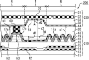
- FIG. 2 is a schematic cross-sectional view showing a specific example of the liquid crystal display device 100 shown in the conceptual diagram.
- the liquid crystal display device 200 shown in FIG. 2 those having the same configuration as that of the liquid crystal display device 100 shown in FIG.
- the liquid crystal display device 200 is manufactured as follows, for example. First, the TFT array substrate 210 will be described. On the main surface of the glass substrate 11 serving as a base material, wirings such as the gate electrode 12 and the Cs wiring 13 and TFTs (not shown) were formed in a desired shape. A gate insulating film 14 was formed so as to cover these wirings and the like, and a source / drain electrode 15 having a desired shape was formed on the gate insulating film 14. Then, an interlayer insulating film 16 was formed on the gate insulating film 14 so as to cover the source / drain electrodes 15.
- the transmissive display region T includes the first projection.
- Recesses 50 were formed simultaneously.
- the height h2 of the obtained protrusion 17a was 0.8 ⁇ m
- the height h3 of the protrusion 17b was 1.0 ⁇ m.
- the depth d1 of the first recess 50 was 0.8 ⁇ m
- the height h2 of the protrusion 17a and the depth d1 of the first recess 50 were equal.
- a transparent electrode (ITO) 18 and a reflective electrode 19 made of an aluminum / molybdenum laminate are formed on the interlayer insulating film 16 on which the protrusions 17a and 17b and the first recess 50 are formed, respectively. Patterned into the desired shape.
- PI resin manufactured by Nissan Chemical Industries, product number SE7942
- the wettability of the PI resin was good, and the alignment film 43 could be formed on the entire surface of the substrate.
- the CF substrate 230 first forms a CF layer 32 made of R (red) G (green) B (blue) having a film thickness of 1.1 ⁇ m on the main surface of the glass substrate 31, and the obtained CF layer 32.
- a transparent resin layer 33 having a thickness of 1.8 ⁇ m was formed so as to cover the surface. Then, the transparent resin layer 33 in the transmissive display region T was subjected to an exposure process to form a second recess 51 having a depth d2 of 1.8 ⁇ m.
- a transparent electrode (ITO) 38 was formed so as to cover the entire surface of the substrate including the second recess 51. Further, in the reflective display region R, PS60 for maintaining the distance between the TFT array substrate 210 and the CF substrate 230 was formed by photolithography.
- the alignment resin 44 was formed by apply
- the TFT array substrate 210 and the CF substrate 230 manufactured as described above are bonded with a sealant (not shown) so that the alignment films 43 and 44 face each other, and liquid crystal is injected between both substrates.
- a liquid crystal layer 20 was formed.
- the thickness s1 in the reflective display region R is 2.3 ⁇ m
- the thickness s2 in the transmissive display region T is 4.6 ⁇ m
- the thickness s1 in the reflective display region R is equal to the thickness s2 in the transmissive display region T. It was about 1/2.
- the protrusions 17a and 17b are formed on the interlayer insulating film 16 in the reflective display region R.
- the present invention is not limited to this, and the protrusions may be formed as necessary.
- the shape, number, etc. are not particularly limited.
- the liquid crystal display device according to the comparative embodiment will be described below with reference to FIGS. 1 having the same configuration as that of the liquid crystal display device 100 shown in FIG.
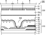
- FIG. 3 is a schematic cross-sectional view showing a configuration of a liquid crystal display device 300 having a TFT multi-gap structure.
- the recess for adjusting the thickness of the liquid crystal layer 20 is formed only in the interlayer insulating film 16a formed on the TFT array substrate 310, and is not formed on the CF substrate 330 side.
- the TFT array substrate 310 is formed with TFTs, transparent electrodes 18, reflective electrodes 19 and the like, the opening of the recess 350 becomes narrower as the pixels become finer, and the bottom of the recess 350 is made of PI resin.
- the wettability is lowered, and a place where the alignment film 45 is not formed is generated like a region surrounded by a wavy line. As a result, the alignment of the liquid crystal molecules is disturbed, and the liquid crystal display device 300 has a display defect.
- FIG. 4 is a schematic cross-sectional view showing a configuration of a liquid crystal display device 400 having a CF multi-gap structure.
- the recess for adjusting the thickness of the liquid crystal layer 20 is formed only in the transparent resin layer 33 b formed on the CF substrate 430, and is not formed on the TFT array substrate 410 side. . Therefore, when the depth of the concave portion 450 is deep, the step of the concave portion 450 becomes large, and the wettability of the PI resin decreases at the bottom edge portion, so that the alignment film 48 is formed like a region surrounded by a wavy line. A place that is not done. As a result, the alignment of the liquid crystal molecules is disturbed, and the liquid crystal display device 400 has a display defect.
Landscapes
- Physics & Mathematics (AREA)
- Nonlinear Science (AREA)
- Mathematical Physics (AREA)
- Chemical & Material Sciences (AREA)
- Crystallography & Structural Chemistry (AREA)
- General Physics & Mathematics (AREA)
- Optics & Photonics (AREA)
- Liquid Crystal (AREA)
- Spectroscopy & Molecular Physics (AREA)
Abstract
本発明は、マルチギャップ構造を有する小型・薄型で高精細化が進んだ液晶表示装置であっても、配向膜材料の濡れ性が良く配向膜不良がないことから、良好な表示特性が得られる液晶表示装置を提供する。本発明の液晶表示装置は、第1の基板、液晶層、及び、第2の基板をこの順に備え、かつ、反射表示領域と透過表示領域とを備えた液晶表示装置であって、上記第1及び第2の基板は、液晶層側の主面上に絶縁膜を有し、上記絶縁膜は、上記透過表示領域において、基板面に対して法線方向から見たときに上記液晶層の厚みを大きくする凹部を、上記第1の基板と第2の基板との両方に有し、上記第1及び第2の基板は、上記液晶層と接する面に上記凹部を含めて覆う配向膜を更に有する。
Description
本発明は、液晶表示装置に関する。より詳しくは、半透過型の液晶表示装置に関するものである。
液晶表示装置は、薄型で軽量かつ低消費電力といった特長を活かし、モニター、プロジェクタ、携帯電話、携帯情報端末(PDA)等の電子機器に幅広く利用されている。中でも、携帯電話、ゲーム機器、車載部品を主体とした中小型の電子機器には、半透過型(反射透過両用型)と呼ばれる液晶表示装置が使用されている。
半透過型の液晶表示装置は、透過表示領域と反射表示領域とを有する。そして、屋内等の比較的に暗い環境下では、透過表示領域において、液晶表示パネルに設けられたバックライト等の背面側からの光を液晶表示パネルの内部に導き、外部に出射して表示を行う透過表示が行われる。また、屋外等の比較的に明るい環境下では、反射表示領域において、周囲やフロントライト等の前面側(観察面側)からの光を液晶表示パネルの内部に導き、この光を反射させて外部に出射して表示を行う反射表示が行われる。これにより、半透過型の液晶表示装置は、明るい環境下、暗い環境下のいずれの環境下においても、優れた視認性を有するものとなる。
半透過型の液晶表示装置においては、透過表示領域では、背面側からの光は、液晶表示パネルに入射してから出射するまでに液晶層を一度しか通過しないのに対し、反射表示領域では、前面側からの光は、液晶表示パネルに入射してから出射するまでに液晶層を二度通過する。そのため、透過表示領域を通過する光と反射表示領域を通過する光との間で位相差が生じる。位相差を解消するためには、透過表示領域における光路長と反射表示領域における光路長とを等しくする必要があることから、反射表示領域における液晶層の厚み(以下「セル厚」ともいう。)を、透過表示領域のセル厚の略1/2としている。
透過表示領域及び反射表示領域のセル厚を制御する方法としては、セル内に凹部や突起等の構造物を設けてセル厚を制御する、いわゆるマルチギャップ構造とする手法が知られている。具体的には、TFTアレイ基板の側に形成された有機絶縁膜に構造物を設けてセル厚を制御する方法(例えば、特許文献1参照。)や、CF(カラーフィルタ)基板の側に形成された透明樹脂層に構造物を設けてセル厚を制御する方法(例えば、特許文献2参照。)がある。以下、前者の方法により形成された構造をTFTマルチギャップ構造、後者の方法により形成された構造をCFマルチギャップ構造と称す。
マルチギャップ構造を有する液晶表示装置においては、装置の高精細化への要望が高まっている。すなわち、マルチギャップ構造を有する半透過型の液晶表示装置は、上述のように中小型の電子機器に搭載されることから、装置の小型化・薄型化に伴って画素の微細化が進んでおり、微細な画素を有する高精細化が進んだ液晶表示装置においても良好な表示特性が得られることが望まれている。
液晶表示装置は、一対の基板間に液晶層を有し、基板と液晶層との間に配向膜が形成された構成を有するが、上記のように液晶表示装置の高精細化が進むと、配向膜を形成するための配向膜材料、具体的には、PI(ポリイミド)樹脂を基板に塗布する際の濡れ性が悪くなることがある。TFTマルチギャップ構造の液晶表示装置であれば、セルを調整するためにTFTアレイ基板の有機絶縁膜に形成された凹部の開口部が狭くなって、PI樹脂の濡れ性が悪くなることがある。また、セル厚の大きいCFマルチギャップ構造の液晶表示装置であれば、セルを調整するためにCF基板に形成された有機絶縁膜(透明樹脂層)の厚みによっては、構造物のうち凹部のエッジ部分の濡れ性が悪くなり、PI樹脂を塗布できないことがある。
PI樹脂によって形成される配向膜は、上述のように、液晶層と接するように形成される膜であり、液晶分子の配向状態を規制するものである。したがって、PI樹脂の濡れ性が悪くなって充分な膜厚の配向膜が形成されなかったり、PI樹脂が塗布されず膜が形成されない場所が生じたりすると、液晶の良好な配向状態が得られず、表示不良が生じる恐れがある。
本発明は、上記現状に鑑みてなされたものであり、マルチギャップ構造を有する小型・薄型で高精細化が進んだ液晶表示装置であっても、配向膜材料の濡れ性が良く配向膜不良がないことから、良好な表示特性が得られる液晶表示装置を提供することを目的とするものである。
本発明者らは、高精細化が進んだマルチギャップ構造を有する液晶表示装置について種々検討したところ、マルチギャップ構造を形成するために絶縁膜に形成される構造物、特に凹部に着目し、配向膜材料の濡れ性は、この凹部に影響を受け、画素の微細化が進んだり、セル厚が厚くなって凹部の深さが深くなると、配向膜材料の濡れ性が低下する傾向にあることをまず見いだした。そして、いずれか一方の基板に凹部が形成されるTFTマルチギャップ構造やCFマルチギャップ構造とは異なり、一対の基板の両方に凹部を形成することでマルチギャップ構造を維持しつつ配向膜材料の濡れ性の低下を抑制できることを見いだし、上記課題をみごとに解決することができることに想到し、本発明に到達したものである。
すなわち、本発明は、第1の基板、液晶層、及び、第2の基板をこの順に備え、かつ、反射表示領域と透過表示領域とを備えた液晶表示装置であって、上記第1及び第2の基板は、液晶層側の主面上に絶縁膜を有し、上記絶縁膜は、上記透過表示領域において、基板面に対して法線方向から見たときに上記液晶層の厚みを大きくする凹部を、上記第1の基板と第2の基板との両方に有し、上記第1及び第2の基板は、上記液晶層と接する面に上記凹部を含めて覆う配向膜を更に有する液晶表示装置である。
本発明の液晶表示装置は、第1の基板、液晶層、及び、第2の基板をこの順に備え、液晶層に印加する電圧を変化させることにより、液晶層のリタデーションを変化させることで表示を行うものである。また、反射表示領域と透過表示領域とを備えた半透過型の液晶表示装置である。
上記第1及び第2の基板は、液晶層側の主面上に絶縁膜を有する。この絶縁膜は、上記透過表示領域において、基板面に対して法線方向から見たときに上記液晶層の厚みを大きくする凹部を、上記第1の基板と第2の基板との両方に有する。これにより、いずれか一方の基板の絶縁膜に凹部が形成されるTFTマルチギャップ構造やCFマルチギャップ構造に比べて一つあたりの凹部の深さを浅くすることができ、微細な画素やセル厚の大きい液晶表示装置であっても、ポリイミド樹脂等の配向膜材料を濡れ性良く塗布できる。なお、透過表示領域において絶縁膜に形成される凹部とは、絶縁膜の膜厚が薄いことで形成される窪みだけではなく、絶縁膜の一部が無いことにより形成される窪みも含む。
上記第1及び第2の基板は、上記液晶層と接する面に上記凹部を含めて覆う配向膜を更に有する。この配向膜は、ポリイミド樹脂により形成されたものであることが好ましい。上記のように、第1の基板と第2の基板との両方の基板に凹部が形成されることで、各々の凹部の深さを配向膜材料の濡れ性の低下が問題とならない程度の深さとすることができる。これにより、微細な画素やセル厚の大きいマルチギャップ構造を有する液晶表示装置であっても、配向膜材料を均一に塗布でき、配向膜不良の大幅な改善が見込める。また、高精細な液晶表示装置についても適用可能であることから、あらゆる配線ピッチの液晶表示装置において良好な表示特性が得られる。
なお、本発明に係る液晶表示装置において、第1及び第2の基板に形成された凹部の存在は、例えば、走査型電子顕微鏡(SEM)等を用いて確認できる。
本発明の液晶表示装置に係る好ましい形態について以下に詳しく説明する。
本発明の液晶表示装置に係る好ましい形態について以下に詳しく説明する。
本発明の液晶表示装置において好ましい形態としては、上記液晶層の厚みは、上記反射表示領域において上記透過表示領域の略1/2であるものが挙げられる。半透過型の液晶表示装置において、反射表示領域と透過表示領域とでは、表示特性上、各領域を透過する光の光路長を等しくすることが望ましい。本発明においては、上記のように反射表示領域と透過表示領域との液晶層の厚みを異ならせることで、各領域を透過する光の光路長を等しくすることができるため望ましい。ここで、略1/2とは、厳密に1/2であることが好ましいが、液晶層を通過する光の光路長を反射表示領域と透過表示領域とにおいて表示品位に実質的な影響を与えない程度に等しくするものであればよい。具体的には、反射表示領域の液晶層の厚みは、透過表示領域の液晶層の厚みの30~70%であることが好ましい。
また、本発明の液晶表示装置において好ましい形態としては、上記第1の基板は、薄膜トランジスタアレイ基板であって、上記基板に形成された絶縁膜は層間絶縁膜であり、上記第2の基板は、カラーフィルタ基板であって、上記基板に形成された絶縁膜は透明樹脂層であり、上記透明樹脂層に形成された凹部の深さは、上記層間絶縁膜に形成された凹部の深さよりも深いものが挙げられる。
薄膜トランジスタアレイ基板においては、TFTと透明電極との間に設けられた層間絶縁膜を利用してマルチギャップ構造が形成される場合があるが、層間絶縁膜の液晶層側の表面には、透明電極や反射電極等が形成されるため、画素の微細化が進むと、構造物の開口部、特に凹部の開口部が小さくなって凹部の底部での配向膜材料の濡れ性が低下する傾向にある。一方、カラーフィルタ基板は、薄膜トランジスタアレイ基板に比べて構成要素が少なく比較的簡易な構成であるため、画素の微細化が進んでも配向膜材料の濡れ性の低下は薄膜トランジスタアレイ基板よりも小さい。しかしながら、セル厚が大きい場合には構造物である凹部の深さが深くなり、凹部の底部におけるエッジ部分で配向膜材料の濡れ性が低下する傾向にある。
そこで、本発明においては、マルチギャップ構造を構成する構造物のうち凹部については、カラーフィルタ基板の透明樹脂層において配向膜材料の濡れ性の低下が問題とならない程度の深さに形成された凹部と、この凹部の深さだけでは所望するマルチギャップ構造に足りない深さを補うための、薄膜トランジスタアレイ基板の層間絶縁膜に形成された凹部とで構成する。このように透明樹脂層に形成された凹部の深さを、層間絶縁膜に形成された凹部の深さよりも深いものとすることで、画素の微細化が進んでも、また、セル厚が厚くなっても、配向膜材料の濡れ性の低下を防止でき、配向膜不良のない液晶表示装置が得られる。
なお、この形態においては、上記透明樹脂層に形成された凹部の深さは、2μm以下であることが好ましい。これは、カラーフィルタ基板では、凹部の深さが2μmを超えると配向膜材料の濡れ性が低下する傾向にあるためである。
また、上記反射表示領域において、上記層間絶縁膜は、上記液晶層の側へ突出した複数の突起物を有し、基板面に対して法線方向から見たときに、上記突起物と重畳して反射膜が配置されていることが好ましい。
上記反射膜は、入射した光を反射させるものであり、基板面に対して法線方向から見たときに、突起物と重畳して配置される突起物によって反射光が乱反射するため、光の干渉が起こらず、表示に干渉縞が発生することを抑制できる。なお、本発明の効果を得ることができる限り、反射膜は全ての突起物に重なる必要はなく、一部に重ならない範囲を有していてもよい。
上記突起物の形成方法は特に限定されるものではないが、TFTアレイ基板を作製する際に適用されるフォトリソグラフィ法、具体的には、フォトマスクに所定の透過率を変化させたパターンを与えることにより、レジストパターン膜の膜厚を局所的に薄くする手法(ハーフトーン露光法)、又は、2つの異なったマスクを用いて、異なった露光量で2回露光する手法(TWIN露光法)を適用すると容易に形成できる。この場合には、上記層間絶縁膜に形成された上記凹部の深さと上記突起物の高さとが実質的に等しいものであると、凹部と突起物とをハーフトーン露光時、又は、TWIN露光時に同時に形成できるためより好ましい。
本発明の液晶表示装置の構成としては、このような構成要素を必須として形成されるものである限り、その他の構成要素により特に限定されるものではない。
本発明の液晶表示装置によれば、微細な画素やセル厚の大きいマルチギャップ構造を有する高精細な液晶表示装置であっても、配向膜材料の濡れ性が良いため配向膜不良がなく、良好な表示特性が得られる。
以下に実施形態を掲げ、本発明を図面を参照して更に詳細に説明するが、本発明はこれらの実施形態のみに限定されるものではない。
実施形態1
以下に、本発明の実施形態1に係る液晶表示装置の構成を概念図を用いて説明する。図1は、本実施形態に係る液晶表示装置の断面構成を示す概念図である。図1において、液晶表示装置100は、第1の基板としてのTFTアレイ基板10、液晶層20、及び、第2の基板としてのCF基板30をこの順に備える。また、反射表示を行う反射表示領域Rと透過表示を行う透過表示領域Tと有する半透過型の液晶表示装置100であり、液晶層20は、反射表示領域Rにおける厚みs1が、透過表示領域Tにおける厚みs2の略1/2となるように構成されたマルチギャップ構造を有する。
以下に、本発明の実施形態1に係る液晶表示装置の構成を概念図を用いて説明する。図1は、本実施形態に係る液晶表示装置の断面構成を示す概念図である。図1において、液晶表示装置100は、第1の基板としてのTFTアレイ基板10、液晶層20、及び、第2の基板としてのCF基板30をこの順に備える。また、反射表示を行う反射表示領域Rと透過表示を行う透過表示領域Tと有する半透過型の液晶表示装置100であり、液晶層20は、反射表示領域Rにおける厚みs1が、透過表示領域Tにおける厚みs2の略1/2となるように構成されたマルチギャップ構造を有する。
TFTアレイ基板10は、ガラス基板11の主面上に、ゲート電極12、ゲート絶縁膜14、ソース・ドレイン電極15、層間絶縁膜16、透明電極18、反射電極(反射膜)19、及び、配向膜41をこの順に備える。
反射表示領域Rにおける層間絶縁膜16の主面には、複数の突起物17が形成されており、基板面に対して法線方向から見たときに、突起物17と重畳するように透明電極18及び反射電極19が配置されている。
また、透過表示領域Tにおける層間絶縁膜16の主面には、セル厚を制御するための第1の凹部50が形成されている。ここで、第1の凹部50の深さd1と突起物17の高さh1とは、実質的に等しい。
CF基板30は、ガラス基板31の主面上に、CF層32、絶縁膜である透明樹脂層33、及び、配向膜42をこの順に備える。CF層32は、例えば、赤(R)、緑(G)、青(B)の各色からなる。透過表示領域Tにおける透明樹脂層33には、セル厚を制御するための第2の凹部51が形成されている。
上記のように液晶表示装置100は、透過表示領域Tにおいて、TFTアレイ基板10及びCF基板30の両方の基板に形成された凹部によってセル厚を制御したマルチギャップ構造を有している。
ここで、第1の凹部50及び第2の凹部51は、第2の凹部51の深さd2が第1の凹部50の深さd1よりも深くなるように形成される。これは、配向膜41、42の材料であるPI樹脂の濡れ性を考慮したものであり、画素の微細化を図っても凹部の開口部が狭くなりにくいCF基板30の側に、より深い凹部を形成するのが良いためである。ただし、第2の凹部51の深さd2があまりに深くなると、第2の凹部51の底部においてエッジ部の濡れ性が低下しやすくなるため、濡れ性が低下しない程度の深さd2に設定する必要がある。この深さは、液晶表示装置のサイズ等によって異なるため適宜設定されるものであるが、例えば、深さd2が2μmを超えると濡れ性の低下が生じやすい。したがって、深さd2は、2μm以下であることが好ましい。
TFTアレイ基板10は、液晶層20と接する面に、第1の凹部50を含めて覆う配向膜41を有する。同様に、CF基板30は、液晶層20と接する面に、第2の凹部51を含めて覆う配向膜42を有する。配向膜41、42は、基板面にPI樹脂を塗布することにより形成されるが、本実施形態においては、上述のように開口部が小さくなりやすいTFTアレイ基板10には、深さd1の浅い第1の凹部50が形成されているため、PI樹脂の濡れ性が低下しにくく、基板の全面に配向膜41を形成できる。一方で、CF基板30には、深さd2の深い第2の凹部51が形成されるが、第1の凹部50とともにセル厚を制御することで濡れ性の低下が問題とならない程度の深さd2に設定できるため、CF基板30にも全面に配向膜42を形成できる。
これにより、本実施形態に係る液晶表示装置100は、微細な画素やセル厚の大きいマルチギャップ構造を有する液晶表示装置であっても、良好な表示特性が得られる。以下に、上記実施形態に係る液晶表示装置100を具体例に基づき説明する。
実施例1
図2は、上記概念図において示した液晶表示装置100の具体例を示す断面模式図である。図2に示す液晶表示装置200において、図1に示す液晶表示装置100と同様の構成を示すものについては、同一の符号を付して以下説明する。
図2は、上記概念図において示した液晶表示装置100の具体例を示す断面模式図である。図2に示す液晶表示装置200において、図1に示す液晶表示装置100と同様の構成を示すものについては、同一の符号を付して以下説明する。
液晶表示装置200は、例えば、以下のようにして製造される。まず、TFTアレイ基板210について説明する。基材となるガラス基板11の主面上に、ゲート電極12、Cs配線13等の配線やTFT(図示せず)を所望の形状に形成した。これらの配線等を覆うようにゲート絶縁膜14を形成し、ゲート絶縁膜14上に、所望の形状のソース・ドレイン電極15を形成した。そして、ソース・ドレイン電極15を覆うようにゲート絶縁膜14上に層間絶縁膜16を形成した。
次いで、層間絶縁膜16の表面にハーフトーン露光処理を施して、反射表示領域Rには突起物17aとPS60を支持するための突起物17bとを形成し、透過表示領域Tには第1の凹部50を、それぞれ同時に形成した。得られた突起物17aの高さh2は、0.8μmであり、突起物17bの高さh3は1.0μmであった。また、第1の凹部50の深さd1は、0.8μmであり、突起物17aの高さh2と第1の凹部50の深さd1とは等しくなった。
次いで、突起物17a、17bと第1の凹部50とが形成された層間絶縁膜16上に、透明電極(ITO)18と、アルミニウム/モリブデンの積層体からなる反射電極19とを形成し、それぞれ所望の形状にパターン形成した。
そして、基板の全面を覆うようにPI樹脂(日産化学工業社製、品番SE7492)を塗布した。このとき、PI樹脂の濡れ性は良好であり、基板の全面に配向膜43を形成できた。
一方、CF基板230は、まず、ガラス基板31の主面上に膜厚1.1μmのR(赤)G(緑)B(青)からなるCF層32を形成し、得られたCF層32を覆うように膜厚1.8μmの透明樹脂層33を形成した。そして、透過表示領域Tにおける透明樹脂層33に露光処理を施して、深さd2が1.8μmである第2の凹部51を形成した。
そして、第2の凹部51を含めて基板全面を覆うように透明電極(ITO)38を形成した。更に、反射表示領域Rには、TFTアレイ基板210とCF基板230との間隔を維持するためのPS60を、フォトリソグラフィにより形成した。
そして、PS60が形成された基板に、上記と同様にPI樹脂を塗布して配向膜44を形成した。このとき、CF基板230においても、PI樹脂の濡れ性は良好であり、基板の全面に配向膜44を形成できた。
上記のように作製されたTFTアレイ基板210とCF基板230とを、配向膜43、44同士が向かい合うようにしてシール剤(図示せず)にて貼り合わせ、両基板間に液晶を注入して液晶層20を形成した。液晶層20の厚みは、反射表示領域Rにおける厚みs1が2.3μmであり、透過表示領域Tにおける厚みs2が4.6μmとなり、反射表示領域Rにおける厚みs1が透過表示領域Tにおける厚みs2の略1/2となっていた。
得られた液晶表示装置200は、配向膜43、44が良好に形成されていたため、配向膜不良に起因する表示不良がなく、表示特性の良いものであった。
なお、上記説明では、反射表示領域Rにおける層間絶縁膜16に突起物17a、17bを形成しているが、本発明はこれに限定されるものではなく、突起物は必要に応じて形成すればよく、その形状や数等は特に限定されるものではない。
以下に、比較実施形態に係る液晶表示装置ついて、図3及び図4を用いて説明する。なお、図1に示す液晶表示装置100と同一の構成を有するものについては同一の符号を付け、説明を省略する。
比較実施形態1
図3は、TFTマルチギャップ構造を有する液晶表示装置300の構成を示す断面模式図である。この液晶表示装置300では、液晶層20の厚みを調整するための凹部は、TFTアレイ基板310に形成された層間絶縁膜16aのみに形成されており、CF基板330の側には形成されていない。TFTアレイ基板310には、TFT、透明電極18、反射電極19等が形成されていることから画素の微細化が進むと凹部350の開口部が狭くなり、凹部350の底部においては、PI樹脂の濡れ性が低下して、波線で囲まれた領域のように配向膜45が形成されていない場所が生じる。これにより液晶分子の配向が乱れ、液晶表示装置300には、表示不良が生じる。
図3は、TFTマルチギャップ構造を有する液晶表示装置300の構成を示す断面模式図である。この液晶表示装置300では、液晶層20の厚みを調整するための凹部は、TFTアレイ基板310に形成された層間絶縁膜16aのみに形成されており、CF基板330の側には形成されていない。TFTアレイ基板310には、TFT、透明電極18、反射電極19等が形成されていることから画素の微細化が進むと凹部350の開口部が狭くなり、凹部350の底部においては、PI樹脂の濡れ性が低下して、波線で囲まれた領域のように配向膜45が形成されていない場所が生じる。これにより液晶分子の配向が乱れ、液晶表示装置300には、表示不良が生じる。
比較実施形態2
図4は、CFマルチギャップ構造を有する液晶表示装置400の構成を示す断面模式図である。この液晶表示装置400では、液晶層20の厚みを調整するための凹部は、CF基板430に形成された透明樹脂層33bのみに形成されており、TFTアレイ基板410の側には形成されていない。そのため、凹部450の深さが深い場合には、凹部450の段差が大きくなって底部のエッジ部でPI樹脂の濡れ性が低下して、波線で囲まれた領域のように配向膜48が形成されていない場所が生じる。これにより液晶分子の配向が乱れ、液晶表示装置400には、表示不良が生じる。
図4は、CFマルチギャップ構造を有する液晶表示装置400の構成を示す断面模式図である。この液晶表示装置400では、液晶層20の厚みを調整するための凹部は、CF基板430に形成された透明樹脂層33bのみに形成されており、TFTアレイ基板410の側には形成されていない。そのため、凹部450の深さが深い場合には、凹部450の段差が大きくなって底部のエッジ部でPI樹脂の濡れ性が低下して、波線で囲まれた領域のように配向膜48が形成されていない場所が生じる。これにより液晶分子の配向が乱れ、液晶表示装置400には、表示不良が生じる。
本願は、2009年1月28日に出願された日本国特許出願2009-16504号を基礎として、パリ条約ないし移行する国における法規に基づく優先権を主張するものである。該出願の内容は、その全体が本願中に参照として組み込まれている。
10、210、310、410 TFTアレイ基板
11、31 ガラス基板
12 ゲート電極
13 Cs配線
14 ゲート絶縁膜
15 ソース・ドレイン電極
16、16a、16b 層間絶縁膜
17、17a、17b 突起物
18、38 透明電極
19 反射電極
20 液晶層
30、230、330、430 CF基板
33、33a、33b 透明樹脂層
32 CF層
41~48 配向膜
50 第1の凹部
51 第2の凹部
60 PS
100、200、300、400 液晶表示装置
350、450 凹部
d1、d2 凹部の深さ
s1、s2 液晶層の厚み
h1、h2、h3 突起物の高さ
R 反射表示領域
T 透過表示領域
11、31 ガラス基板
12 ゲート電極
13 Cs配線
14 ゲート絶縁膜
15 ソース・ドレイン電極
16、16a、16b 層間絶縁膜
17、17a、17b 突起物
18、38 透明電極
19 反射電極
20 液晶層
30、230、330、430 CF基板
33、33a、33b 透明樹脂層
32 CF層
41~48 配向膜
50 第1の凹部
51 第2の凹部
60 PS
100、200、300、400 液晶表示装置
350、450 凹部
d1、d2 凹部の深さ
s1、s2 液晶層の厚み
h1、h2、h3 突起物の高さ
R 反射表示領域
T 透過表示領域
Claims (6)
- 第1の基板、液晶層、及び、第2の基板をこの順に備え、かつ、反射表示領域と透過表示領域とを備えた液晶表示装置であって、
該第1及び第2の基板は、液晶層側の主面上に絶縁膜を有し、
該絶縁膜は、該透過表示領域において、基板面に対して法線方向から見たときに該液晶層の厚みを大きくする凹部を、該第1の基板と第2の基板との両方に有し、
該第1及び第2の基板は、該液晶層と接する面に該凹部を含めて覆う配向膜を更に有することを特徴とする液晶表示装置。 - 前記液晶層の厚みは、前記反射表示領域において前記透過表示領域の略1/2であることを特徴とする請求項1記載の液晶表示装置。
- 前記第1の基板は、薄膜トランジスタアレイ基板であって、該基板に形成された絶縁膜は層間絶縁膜であり、
前記第2の基板は、カラーフィルタ基板であって、該基板に形成された絶縁膜は透明樹脂層であり、
該透明樹脂層に形成された凹部の深さは、該層間絶縁膜に形成された凹部の深さよりも深いことを特徴とする請求項1又は2記載の液晶表示装置。 - 前記透明樹脂層に形成された凹部の深さは、2μm以下であることを特徴とする請求項3記載の液晶表示装置。
- 前記反射表示領域において、前記層間絶縁膜は、前記液晶層の側へ突出した複数の突起物を有し、基板面に対して法線方向から見たときに、該突起物と重畳して反射膜が配置されていることを特徴とする請求項3又は4記載の液晶表示装置。
- 前記層間絶縁膜に形成された前記凹部の深さと前記突起物の高さとが実質的に等しいことを特徴とする請求項5記載の液晶表示装置。
Applications Claiming Priority (2)
| Application Number | Priority Date | Filing Date | Title |
|---|---|---|---|
| JP2009-016504 | 2009-01-28 | ||
| JP2009016504 | 2009-01-28 |
Publications (1)
| Publication Number | Publication Date |
|---|---|
| WO2010087045A1 true WO2010087045A1 (ja) | 2010-08-05 |
Family
ID=42395313
Family Applications (1)
| Application Number | Title | Priority Date | Filing Date |
|---|---|---|---|
| PCT/JP2009/064796 Ceased WO2010087045A1 (ja) | 2009-01-28 | 2009-08-25 | 液晶表示装置 |
Country Status (1)
| Country | Link |
|---|---|
| WO (1) | WO2010087045A1 (ja) |
Citations (1)
| Publication number | Priority date | Publication date | Assignee | Title |
|---|---|---|---|---|
| JP2007316664A (ja) * | 2001-10-02 | 2007-12-06 | Sharp Corp | 液晶表示装置の製造方法 |
-
2009
- 2009-08-25 WO PCT/JP2009/064796 patent/WO2010087045A1/ja not_active Ceased
Patent Citations (1)
| Publication number | Priority date | Publication date | Assignee | Title |
|---|---|---|---|---|
| JP2007316664A (ja) * | 2001-10-02 | 2007-12-06 | Sharp Corp | 液晶表示装置の製造方法 |
Similar Documents
| Publication | Publication Date | Title |
|---|---|---|
| JP4762297B2 (ja) | 液晶表示装置 | |
| US8390770B2 (en) | Liquid crystal display, color filter substrate and manufacturing method thereof | |
| US9454034B2 (en) | Color filter array substrate, method for fabricating the same and display device | |
| JP2009133948A (ja) | 液晶装置、液晶装置の製造方法、電子機器 | |
| JP2017067999A (ja) | 電気光学装置用基板、電気光学装置、電子機器 | |
| JP2008233860A (ja) | 液晶装置とその製造方法、電子機器 | |
| JP2008309977A (ja) | 液晶装置および電子機器 | |
| US20140078452A1 (en) | Transreflective color filter and method for manufacturing the same and method for manufacturing the same and liquid crystal display device | |
| US7570337B2 (en) | Display device | |
| WO2011027602A1 (ja) | 液晶表示装置 | |
| US20090075189A1 (en) | Methods for fabricating transflective liquid crystal displays | |
| KR100529657B1 (ko) | 액정 표시장치 및 그 제조방법 | |
| US8094268B2 (en) | Liquid crystal display substrate, liquid crystal display device and manufacturing method of the liquid crystal display substrate | |
| US8314905B2 (en) | Transflective liquid crystal display panel and electronic apparatus | |
| CN101833193B (zh) | 半透过式液晶显示器、透明基板及其制造方法 | |
| WO2009113206A1 (ja) | 液晶表示装置 | |
| JP5655426B2 (ja) | カラーフィルタの製造方法およびカラーフィルタ | |
| JP4900073B2 (ja) | 液晶装置および電子機器 | |
| US9081224B2 (en) | Transflective liquid crystal display panel and liquid crystal display | |
| WO2010087045A1 (ja) | 液晶表示装置 | |
| KR100805493B1 (ko) | 액정 장치 및 전자기기 | |
| JP4131520B2 (ja) | 液晶表示装置 | |
| TWI898534B (zh) | 彩色濾光片基板及顯示裝置 | |
| JP5334012B2 (ja) | 半透過型液晶表示パネル及び電子機器 | |
| US20110090440A1 (en) | Liquid crystal device, method of manufacturing the same, and electronic apparatus |
Legal Events
| Date | Code | Title | Description |
|---|---|---|---|
| 121 | Ep: the epo has been informed by wipo that ep was designated in this application |
Ref document number: 09839234 Country of ref document: EP Kind code of ref document: A1 |
|
| NENP | Non-entry into the national phase |
Ref country code: DE |
|
| NENP | Non-entry into the national phase |
Ref country code: JP |
|
| 122 | Ep: pct application non-entry in european phase |
Ref document number: 09839234 Country of ref document: EP Kind code of ref document: A1 |