WO2010073389A1 - 通信装置および通信方法 - Google Patents
通信装置および通信方法 Download PDFInfo
- Publication number
- WO2010073389A1 WO2010073389A1 PCT/JP2008/073807 JP2008073807W WO2010073389A1 WO 2010073389 A1 WO2010073389 A1 WO 2010073389A1 JP 2008073807 W JP2008073807 W JP 2008073807W WO 2010073389 A1 WO2010073389 A1 WO 2010073389A1
- Authority
- WO
- WIPO (PCT)
- Prior art keywords
- signal
- transmission signal
- unit
- digital
- digital signal
- Prior art date
- Legal status (The legal status is an assumption and is not a legal conclusion. Google has not performed a legal analysis and makes no representation as to the accuracy of the status listed.)
- Ceased
Links
Images





Classifications
-
- H—ELECTRICITY
- H04—ELECTRIC COMMUNICATION TECHNIQUE
- H04B—TRANSMISSION
- H04B1/00—Details of transmission systems, not covered by a single one of groups H04B3/00 - H04B13/00; Details of transmission systems not characterised by the medium used for transmission
- H04B1/38—Transceivers, i.e. devices in which transmitter and receiver form a structural unit and in which at least one part is used for functions of transmitting and receiving
- H04B1/40—Circuits
- H04B1/403—Circuits using the same oscillator for generating both the transmitter frequency and the receiver local oscillator frequency
- H04B1/406—Circuits using the same oscillator for generating both the transmitter frequency and the receiver local oscillator frequency with more than one transmission mode, e.g. analog and digital modes
-
- H—ELECTRICITY
- H04—ELECTRIC COMMUNICATION TECHNIQUE
- H04B—TRANSMISSION
- H04B1/00—Details of transmission systems, not covered by a single one of groups H04B3/00 - H04B13/00; Details of transmission systems not characterised by the medium used for transmission
- H04B1/005—Details of transmission systems, not covered by a single one of groups H04B3/00 - H04B13/00; Details of transmission systems not characterised by the medium used for transmission adapting radio receivers, transmitters andtransceivers for operation on two or more bands, i.e. frequency ranges
- H04B1/0053—Details of transmission systems, not covered by a single one of groups H04B3/00 - H04B13/00; Details of transmission systems not characterised by the medium used for transmission adapting radio receivers, transmitters andtransceivers for operation on two or more bands, i.e. frequency ranges with common antenna for more than one band
- H04B1/0057—Details of transmission systems, not covered by a single one of groups H04B3/00 - H04B13/00; Details of transmission systems not characterised by the medium used for transmission adapting radio receivers, transmitters andtransceivers for operation on two or more bands, i.e. frequency ranges with common antenna for more than one band using diplexing or multiplexing filters for selecting the desired band
Definitions
- the present invention relates to a communication apparatus and a communication method in which a plurality of wireless systems coexist.
- the above-described conventional technique has a problem that when a plurality of wireless systems coexist, it is difficult to perform a stable operation with respect to a temperature change and a change with time.
- an object of the present invention is to provide a communication device that operates stably against temperature changes and changes over time even when a plurality of wireless systems coexist. It is another object of the present invention to provide a communication apparatus that realizes low distortion and high efficiency characteristics at low cost.
- the first conversion unit when the first transmission signal from the first communication system is a digital signal, the first conversion unit that converts the first transmission signal into an analog signal; A second conversion unit that converts the second transmission signal into an analog signal when the second transmission signal from the second communication system different from the first communication system is a digital signal; A combining unit that combines the first transmission signal output from the conversion unit and the second transmission signal output from the second conversion unit, and a peak reduction process on the signal combined by the combining unit And an amplifying unit that amplifies by predistortion correction.
- FIG. 1 is a diagram illustrating a configuration of a wireless communication system including a single base station.
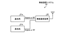
- FIG. 2 is a diagram illustrating a configuration of a wireless communication system including a plurality of base stations.
- FIG. 3 is a diagram showing a configuration of the wireless communication apparatus shown in FIG.
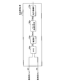
- FIG. 4 is a functional block diagram of the configuration of the wireless communication apparatus according to the first embodiment.
- FIG. 5 is a functional block diagram illustrating the configuration of the modulation unit.
- FIG. 6 is a functional block diagram illustrating a configuration of the demodulation unit.
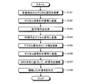
- FIG. 7 is a flowchart of a process procedure performed by the wireless communication apparatus according to the first embodiment.
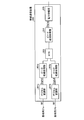
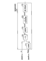
- FIG. 8 is a functional block diagram of the configuration of the wireless communication apparatus according to the second embodiment.
- FIG. 1 is a diagram illustrating a configuration of a wireless communication system including a single base station.
- FIG. 2 is a diagram illustrating a configuration of a wireless communication system including a plurality of base stations.
- FIG. 10 is a functional block diagram (1) illustrating another configuration example of the wireless communication apparatus illustrated in the first embodiment.
- FIG. 11 is a functional block diagram (2) illustrating another configuration example of the wireless communication apparatus illustrated in the first embodiment.
- FIG. 12 is a functional block diagram (3) illustrating another configuration example of the wireless communication apparatus illustrated in the first embodiment.
- FIG. 13 is a functional block diagram (1) illustrating another configuration example of the wireless communication apparatus illustrated in the second embodiment.
- FIG. 14 is a functional block diagram (2) illustrating another configuration example of the wireless communication apparatus illustrated in the second embodiment.
- FIG. 1 is a diagram illustrating a configuration of a wireless communication system including a single base station
- FIG. 2 is a diagram illustrating a configuration of a wireless communication system including a plurality of base stations.
- the wireless communication system 10 includes a single base station (BS ⁇ Base Station> Cabinet) 11 and a wireless communication device (Radio Equipment) 12.
- the base station 11 is a device that performs data communication with a terminal device (not shown; the same applies hereinafter) via the wireless communication device 12.
- the base station 11 transmits the received information to the wireless communication device 12 using a digital signal or an RF (Radio Frequency) signal. Output.
- the wireless communication device 12 is a device that, when receiving a digital signal or an RF signal from the base station 11, compensates for distortion of the received signal, amplifies the signal, and outputs the amplified signal to the terminal device.
- the system configuration of the wireless communication system is the configuration shown in FIG.
- the wireless communication device 22 When the wireless communication device 22 receives digital signals or RF signals from the base stations 21a and 21b, the wireless communication device 22 combines the acquired signals, performs distortion compensation for the combined signals, amplifies the signals, and transmits the amplified signals to the terminal. It is a device that outputs to the device.
- FIG. 3 is a diagram showing a configuration of the wireless communication device 22 shown in FIG. Note that the wireless communication device 22 illustrated in FIG. 3 performs signal distortion compensation by an FF (Feed-Forward) method, and the base stations 21 a and 21 b output RF to the wireless communication device 22. .
- FF Freed-Forward
- the wireless communication device 22 includes a HYB 22a and a PA (power amplifier) 22b.
- the HYB 22a is a device that combines the RF signal transmitted from the base station 21a and the RF signal transmitted from the base station 21b, and outputs the combined RF signal to the PA 22b.
- the PA 22b is a device that, when acquiring the synthesized RF signal output from the HYB 22a, performs distortion correction of the RF signal by the FF method, amplifies the RF signal, and outputs the amplified RF signal to the terminal device. is there.
- each transmission signal in a plurality of base stations is subjected to signal synthesis at the RF signal stage, and then is commonly amplified by an FF power amplifier, Multiple systems can be shared.
- the FF method used by the wireless communication device 22 shown in FIG. 3 has a problem that it is difficult to be stable with respect to changes in temperature and changes over time, so that when a plurality of wireless systems coexist, the wireless communication system is stable. It may not be possible to operate.
- the wireless communication apparatus converts a digital signal into an analog signal (RF signal) when a signal transmitted from each base station is digital when a plurality of wireless communication systems coexist.
- RF signal analog signal
- Each signal is synthesized at an analog signal stage, and after the synthesized signal is demodulated into a digital signal, peak reduction processing, distortion correction, and signal amplification are executed. This enables stable operation against temperature changes and changes with time. In addition, low distortion and high efficiency can be realized at low cost.
- FIG. 4 is a functional block diagram of the configuration of the wireless communication apparatus according to the first embodiment.
- the wireless communication device 100 includes a modulation unit (MOD) 101a, 101b, a HYB 102, a demodulation unit (DEM) 103, a peak reduction processing unit (PAPR reduction) 104, a power amplification unit ( Digital Predistortion) 105.
- the modulation unit 101a may not be provided.
- the modulator 101b may not be provided.
- the modulation unit 101a is a processing unit that modulates a digital signal input from the base station 21a into an RF signal. Modulation section 101a outputs the modulated RF signal to HYB102.
- FIG. 5 is a functional block diagram showing the configuration of the modulation unit 101a.
- the modulation unit 101a includes a digital gain control unit (Digital Gain Control) 111, a first frequency conversion unit (Digital Up Converter) 112, a D / A (Digital / Analog) unit 113, And a second frequency converter 114 (Analog Up Converter).
- Digital Gain Control Digital Gain Control
- first frequency conversion unit Digital Up Converter
- D / A Digital / Analog
- second frequency converter Analog Up Converter
- the digital gain control unit 111 controls the gain (gain) with respect to the acquired digital signal, and outputs the digital signal adjusted according to the controlled gain to the first frequency conversion unit 112. Is a processing unit.
- the first frequency conversion unit 112 when acquiring a digital signal from the digital gain control unit 111, adjusts the frequency of the acquired digital signal to a predetermined frequency (increases the frequency of the input signal to a predetermined frequency). It is.
- the first frequency conversion unit 112 outputs a digital signal adjusted to a predetermined frequency to the D / A unit 113.
- the predetermined frequency is a local frequency of the demodulation unit 103.
- the D / A unit 113 is a processing unit that converts the acquired digital signal into an analog signal (RF signal) when the digital signal is acquired from the first frequency conversion unit 112.
- the D / A unit 113 outputs the converted analog signal to the second frequency conversion unit 114.
- the second frequency conversion unit 114 When the second frequency conversion unit 114 acquires an analog signal from the D / A unit 113, the second frequency conversion unit 114 adjusts the frequency of the acquired analog signal to a predetermined frequency (the frequency of the input signal is increased to a predetermined frequency). It is. The second frequency conversion unit 114 outputs an analog signal adjusted to a predetermined frequency to the HYB 102.
- the predetermined frequency is a local frequency of the demodulation unit 103.
- the modulation unit 101b is a processing unit that modulates a digital signal input from the base station 21b into an RF signal. Modulation section 101b outputs the modulated RF signal to HYB102.
- the configuration of the modulation unit 101b is the same as that of the modulation unit 101a shown in FIG.
- the HYB 102 is a processing unit that combines the RF signal output from the modulation unit 101a and the RF signal output from the modulation unit 101b.
- the HYB 102 outputs the combined RF signal to the demodulation unit 103. In this way, since the HYB 102 synthesizes the signals transmitted from the base stations at the RF signal stage, even when the base clocks of the base stations are not the same, a plurality of wireless communication systems can be easily shared. Can be realized.
- the demodulation unit 103 is a processing unit that demodulates the acquired RF signal into a digital signal when the RF signal output from the HYB 102 is acquired.
- FIG. 6 is a functional block diagram illustrating the configuration of the demodulation unit 103.
- the demodulating unit 103 includes a third frequency converting unit (Analog Down Converter) 121, an A / D (Analog / Digital) unit 122, a fourth frequency converting unit (Digital Down Converter) 123, and And a digital gain control unit 124.
- Analog Down Converter Analog Down Converter
- a / D Analog / Digital
- the third frequency converter 121 is a processing unit that adjusts the frequency of the acquired RF signal to a predetermined frequency (lowers the frequency of the input signal to a predetermined frequency) when the RF signal is acquired from the HYB 102. is there.
- the third frequency converter 121 outputs an RF signal adjusted to a predetermined frequency to the A / D unit 122.
- the predetermined frequency is a local frequency of the demodulation unit 103.
- the A / D unit 122 is a processing unit that converts the acquired RF signal (analog signal) into a digital signal when the RF signal is acquired from the third frequency conversion unit 121.
- the A / D unit 122 outputs the converted digital signal to the fourth frequency conversion unit 123.
- the fourth frequency conversion unit 123 is a processing unit that adjusts the acquired digital signal to a predetermined frequency (lowers the frequency of the input signal to a predetermined frequency) when the digital signal is acquired from the A / D unit 122. .
- the fourth frequency converter 123 outputs a digital signal adjusted to a predetermined frequency to the digital gain controller 124.
- the predetermined frequency is a local frequency of the demodulation unit 103.
- the digital gain control unit 124 When the digital gain control unit 124 acquires a digital signal from the fourth frequency conversion unit 123, the digital gain control unit 124 controls a gain (gain) with respect to the acquired digital signal, and converts the digital signal to the peak reduction processing unit 104 according to the controlled gain. It is a processing part to output.
- the peak reduction processing unit 104 acquires a digital signal from the demodulation unit 103, the peak value of the acquired digital signal (maximum value of the amplitude of the signal) is included in the predetermined threshold value.
- a processing unit for adjusting the digital signal The peak reduction processing unit 104 outputs the digital signal whose peak value has been adjusted to the power amplification unit 105.
- the power amplification unit 105 linearly amplifies a signal having a large peak power to average power ratio (Peak to Average Power Ratio), the power efficiency may be reduced.
- the peak reduction processing unit 104 can output a signal with a small peak power to average power ratio to the power amplification unit 105 by reducing the peak value of the digital signal. it can.
- the power amplifying unit 105 is a processing unit that converts a digital signal into an RF signal and then amplifies the converted RF signal with low distortion based on a DPD (Digital Pre-distortion) method.
- the power amplification unit 105 outputs the power amplified RF signal to the terminal device.
- the process of converting the digital signal into the RF signal is the same as that of the modulation units 101a and 101b described above.
- the power amplifying unit 105 predicts distortion that occurs when the RF signal is amplified, and before actually amplifying the RF signal, for example, the linearizer circuit performs RF processing so that the amplitude and phase are the same as the predicted distortion. After distorting the signal, the RF signal is amplified to cancel the distortion that occurs in the RF signal during amplification.
- FIG. 7 is a flowchart of a process procedure performed by the wireless communication apparatus 100 according to the first embodiment.
- the wireless communication apparatus 100 receives digital signals from the base stations 21a and 21b (step S101), and the modulation units 101a and 101b convert the digital signals into RF signals (step S102). .
- the HYB 102 synthesizes each RF signal (step S103), the demodulator 103 converts the synthesized RF signal into a digital signal (step S104), and the peak reduction processing unit 104 reduces the peak value of the digital signal. (Step S105).
- the power amplification unit 105 converts the digital signal into an RF signal (step S106), amplifies the RF signal based on the DPD method (step S107), and outputs the amplified RF signal (step S108).
- the demodulation unit 103 performs RF processing after the HYB 102 synthesizes the signals at the RF signal stage.
- the signal is converted into a digital signal
- the peak reduction processing unit 104 reduces the peak value of the digital signal
- the power amplification unit 105 returns the digital signal to the RF signal, and executes power amplification of the RF signal based on the DPD method.
- the modulation units 101a and 101b and the demodulation unit 103 change the frequency of the signal, so that the frequency shift function can be easily realized.
- the modulation units 101a and 101b and the demodulation unit 103 change the gain for the signal, so that the output level can be easily changed according to the external device.
- the wireless communication apparatus 100 may be provided with a fixed delay function in the modulation units 101 a and 101 b and the demodulation unit 103. As described above, by providing a signal fixed delay function in the modulation units 101a and 101b and the demodulation unit 103, the wireless communication apparatus 100 can individually control the transmission timing.
- the HYB 102 since the HYB 102 synthesizes each signal at the stage of the RF signal, even if the reference clocks of the base stations (wireless communication systems) are not identical, Sharing is possible.
- the wireless communication apparatus 200 according to the second embodiment When a plurality of wireless communication systems coexist, when the signal transmitted from each base station is an analog signal, the wireless communication apparatus 200 according to the second embodiment converts the analog signal into a digital signal, and The peak reduction process is executed. Then, after executing the peak reduction process, the signals are combined, the peak reduction process is performed again, and the distortion correction and signal amplification of the signal are executed. This enables stable operation against temperature changes and changes with time. In addition, low distortion and high efficiency can be realized at low cost.
- FIG. 8 is a functional block diagram of the configuration of the wireless communication apparatus 200 according to the second embodiment.
- the wireless communication device 200 includes digital modulation units (DEM) 201a and 201b, peak reduction processing units 202a, 202b, and 204, a HYB 203, and a power amplification unit 205.
- DEM digital modulation units
- the digital conversion unit 201a may not be provided.
- the digital conversion unit 201b may not be provided.
- the digital modulation unit 201a is a modulation unit that modulates an RF signal input from the base station 21a into a digital signal.
- the digital modulation unit 201a outputs the converted digital signal to the peak reduction processing unit 202a.
- the specific configuration of the digital modulation unit 201a is the same as that of the demodulation unit 103 (see FIG. 6) described in the first embodiment, and thus description thereof is omitted.
- the digital modulation unit 201b is a modulation unit that modulates an RF signal input from the base station 21b into a digital signal.
- the digital modulation unit 201b outputs the modulated digital signal to the peak reduction processing unit 202b.
- the specific configuration of the digital modulation unit 201b is the same as that of the demodulation unit 103 (see FIG. 6) illustrated in the first embodiment, and thus description thereof is omitted.
- the peak reduction processing unit 202a is a processing unit that adjusts a digital signal so that the peak value of the acquired digital signal is included in a predetermined threshold when the digital signal is acquired from the digital modulation unit 201a.
- the peak reduction processing unit 202a outputs a digital signal whose peak value has been adjusted to the HYB 203.
- the peak reduction processing unit 202b is a processing unit that adjusts a digital signal so that the peak value of the acquired digital signal is included in a predetermined threshold when the digital signal is acquired from the digital modulation unit 201b.
- the peak reduction processing unit 202b outputs a digital signal whose peak value has been adjusted to the HYB 203.
- the peak reduction processing unit 202 is installed for each signal transmitted from each of the base stations 21a and 21b to adjust the peak value, the peak value of the signal is compared with the wireless communication device 100 of the first embodiment. Can be adjusted to a more optimal value.
- the HYB 203 is a processing unit that acquires digital signals output from the peak reduction processing units 202a and 202b and synthesizes the acquired digital signals.
- the HYB 203 outputs the combined digital signal to the peak reduction processing unit 204.
- the peak reduction processing unit 204 is a processing unit that adjusts the digital signal again so that the peak value of the acquired digital signal is included in a predetermined threshold value.
- the peak reduction processing unit 204 outputs the digital signal whose peak value has been adjusted to the power amplification unit 205.
- the power amplifying unit 205 is a processing unit that, after converting a digital signal into an RF signal, amplifies the power of the converted RF signal with low distortion based on the DPD method.
- the power amplifying unit 205 outputs the power amplified RF signal to the terminal.
- the process of converting the digital signal into the RF signal is the same as that of the modulation units 101a and 101b (see FIG. 5) shown in the first embodiment.
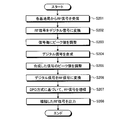
- FIG. 9 is a flowchart of a process procedure performed by the wireless communication apparatus 200 according to the second embodiment.
- the wireless communication apparatus 200 receives RF signals from the base stations 21a and 21b (step S201), and the digital modulation units 201a and 201b convert the RF signals into digital signals (step S202). .
- the peak reduction processing units 202a and 202b adjust the peak value for each signal (step S203), the HYB 203 synthesizes the digital signal (step S204), and the peak reduction processing unit 204 adjusts the peak value of the digital signal. (Step S205).
- the power amplification unit 205 converts the digital signal into an RF signal (step S206), amplifies the RF signal based on the DPD method (step S207), and outputs the amplified RF signal (step S208).
- the wireless communication apparatus 200 when receiving a signal from a plurality of wireless systems, the wireless communication apparatus 200 according to the second embodiment synthesizes each signal after performing peak reduction processing for each signal, and again peaks. In addition to performing reduction processing, signal distortion correction and signal amplification are executed. This enables stable operation against temperature changes and changes with time. In addition, low distortion and high efficiency can be realized at low cost.
- FIGS. 10 to 12 are functional block diagrams showing other configuration examples of the wireless communication apparatus shown in the first embodiment.
- the wireless communication device 100a includes a HYB 102a, a demodulation unit 103a, a peak reduction processing unit 104a, and a power amplification unit 105a.
- signals transmitted from the base stations 21a and 21b are RF signals.
- the wireless communication device 100a Since the signals transmitted from the base stations 21a and 21b are RF signals, as shown in FIG. 10, the wireless communication device 100a has modulation units 101a and 101b as compared to the wireless communication device 100 of FIG. Not.
- the HYB 102a is a processing unit that synthesizes the received RF signals when the RF signals are received from the base stations 21a and 21b.
- the HYB 102a outputs the synthesized RF signal to the demodulation unit 103b.
- the description regarding the demodulation part 103a, the peak reduction process part 104a, and the power amplification part 105a is the same as that regarding the demodulation part 103, the peak reduction process part 104, and the power amplification part 105 of FIG.
- the wireless communication device 100 b includes a modulation unit 101 b, a HYB 102 b, a demodulation unit 103 b, a peak reduction processing unit 104 b, and a power amplification unit 105 b.
- a signal transmitted from the base station 21a is an RF signal
- a signal transmitted from the base station 21b is a digital signal.
- the explanation about the modulation unit 101b, the demodulation unit 103b, the peak reduction processing unit 104b, and the power amplification unit 105b is the same as the explanation about the modulation unit 101b, the demodulation unit 103, the peak reduction processing unit 104, and the power amplification unit 105 in FIG. It is.
- the HYB 102b is a processing unit that synthesizes the acquired RF signal when the RF signal is acquired from the base station 21a and the RF signal is acquired from the modulation unit 101b.
- the HYB 102b outputs the synthesized RF signal to the demodulation unit 103b.
- the signal transmitted from the base station 21a is an RF signal and the signal transmitted from the base station 21b is a digital signal.
- the signal transmitted from the base station 21a is a digital signal.
- a modulation unit can be arranged on the path from the base station 21a to the HYB 102b, and the modulation unit 101b can be excluded.
- the wireless communication device 100c includes modulation units 101a and 101b, a HYB 102c, a demodulation unit 103c, a peak reduction processing unit 104c, and a power amplification unit 105c. And SW (switches) 106a and 106b.
- the modulation units 101a and 101b, the demodulation unit 103c, the peak reduction processing unit 104c, and the power amplification unit 105c are described in the modulation units 101a and 101b, the demodulation unit 103, the peak reduction processing unit 104, and the power amplification unit 105 in FIG. It is the same.
- the SW 106a When the signal transmitted from the base station 21b is an RF signal, the SW 106a outputs the RF signal to the HYB 102c. When the signal transmitted from the base station 21a is a digital signal, the SW 106a passes through the modulation unit 101a. , A switch that acquires an RF signal and outputs the acquired signal to the HYB 102c.
- the SW 106b When the signal transmitted from the base station 21a is an RF signal, the SW 106b outputs the RF signal to the HYB 102c. When the signal transmitted from the base station 21b is a digital signal, the SW 106b passes through the modulation unit 101b. , A switch that acquires an RF signal and outputs the acquired signal to the HYB 102c.
- FIGS. 13 and 14 are functional block diagrams illustrating other configuration examples of the wireless communication apparatus illustrated in the second embodiment.
- the wireless communication device 200a includes a digital modulation unit 201a, peak reduction processing units 202a, 202b, and 204a, a HYB 203a, and a power amplification unit 205a.
- the peak reduction processing unit 202b is a processing unit that requests a digital signal so that the peak value of the acquired digital signal is included in a predetermined threshold when the digital signal is acquired from the base station 21b.
- the peak reduction processing unit 202b outputs a digital signal whose peak value has been adjusted to the HYB 203a.
- the description regarding the peak reduction processing units 202a, 202b, 204a, the HYB 203a, and the power amplification unit 205a is the same as the description regarding the peak reduction processing units 202a, 202b, 204, HYB 203, and the power amplification unit 205 shown in FIG. .
- the signal transmitted from the base station 21a is an RF signal and the signal transmitted from the base station 21b is a digital signal.
- the signal transmitted from the base station 21a is a digital signal.
- a digital modulation unit can be arranged on the path from the base station 21b to the peak reduction processing unit 202b, and the digital modulation unit 201a can be excluded.
- the wireless communication device 200 b includes the digital modulation units 201 a and 201 b, the peak reduction processing units 202 a, 202 b, and 204 c, the HYB 203 c, and the power amplification unit 205 c. And SW (switches) 206a and 206b.
- the explanation regarding the digital modulation units 201a and 201b, the peak reduction processing units 202a, 202b and 204c, the HYB 203c, and the power amplification unit 205c is as follows. This is the same as the description regarding the HYB 203 and the power amplifying unit 205.
- the SW 206a outputs the digital signal to the peak reduction processing unit 202a when the signal transmitted from the base station 21a is a digital signal, and performs digital modulation when the signal transmitted from the base station 21a is an RF signal. It is a switch that acquires a digital signal via the unit 201a and outputs the acquired signal to the peak reduction processing unit 202a.
- the SW 206b outputs the digital signal to the peak reduction processing unit 202b when the signal transmitted from the base station 21b is a digital signal, and performs digital modulation when the signal transmitted from the base station 21b is an RF signal.
- each component of each illustrated apparatus is functionally conceptual and does not necessarily need to be physically configured as illustrated.
- the specific form of distribution / integration of each device is not limited to that shown in the figure, and all or a part thereof may be functionally or physically distributed or arbitrarily distributed in arbitrary units according to various loads or usage conditions. Can be integrated and configured.
- all or any part of each processing function performed in each device may be realized by a CPU and a program analyzed and executed by the CPU, or may be realized as hardware by wired logic.
- Each process described in the present embodiment can be realized by executing a prepared program on a computer such as a personal computer or a workstation.
- This program can be distributed via a network such as the Internet.
- the program can also be executed by being recorded on a computer-readable recording medium such as a hard disk, a flexible disk (FD), a CD-ROM, an MO, and a DVD and being read from the recording medium by the computer.
- a computer-readable recording medium such as a hard disk, a flexible disk (FD), a CD-ROM, an MO, and a DVD and being read from the recording medium by the computer.
Landscapes
- Engineering & Computer Science (AREA)
- Computer Networks & Wireless Communication (AREA)
- Signal Processing (AREA)
- Amplifiers (AREA)
- Transmitters (AREA)
Abstract
第1の通信システムからの第1の送信信号がデジタル信号である場合は、該第1の送信信号をアナログ信号に変換する第1の変換部と、前記第1の通信システムとは異なる第2の通信システムからの第2の送信信号がデジタル信号である場合は、該第2の送信信号をアナログ信号に変換する第2の変換部と、前記第1の変換部から出力された前記第1の送信信号と、前記第2の変換部から出力された前記第2の送信信号とを合成する合成部と、前記合成部で合成された信号をピーク低減処理するとともに前置歪補正により増幅する増幅部と、を備えた通信装置を用いる。温度変化や経時変化に対する安定動作を可能にし、低歪かつ高効率な特性を低コストで実現する。
Description
この発明は、複数の無線システムを共存させる通信装置および通信方法に関するものである。
無線通信の分野では、技術発展に伴い、新しい通信方式による無線システムが構築され、通信サービスが提供される。その際、通常多くのユーザは、すぐに新しい通信サービスに移行するわけではなく、徐々に新サービスに移行していくため、複数の通信サービスが共存して運用されることになる。
一方で、複数の無線システムを共存させた際に発生し得る各種の問題を解消する研究もなされている。例えば、各受信装置に要求される受信品質が異なる複数のシステムの信号に対して、システム毎に適当なピーク抑圧度でピーク抑圧を行う技術が知られている(例えば、特許文献1参照)。また、各変調器に入力される信号のクロック周期を互いに一致しないようにすることで、合成波の包絡線の最大振幅を減少させ、電力増幅器で発生する非線形歪の影響を低減するという技術も知られている(例えば、特許文献2参照)。
しかしながら、上述した従来の技術では、複数の無線システムを共存させた場合に、温度変化や経時変化に対する安定動作が難しいという問題があった。
そこで、複数の無線システムを共存させた場合でも、温度変化や経時変化に対して安定動作する通信装置を提供することを目的とする。また、低歪かつ高効率な特性を低コストで実現する通信装置を提供することを目的とする。
本発明の一態様によれば、第1の通信システムからの第1の送信信号がデジタル信号である場合は、該第1の送信信号をアナログ信号に変換する第1の変換部と、前記第1の通信システムとは異なる第2の通信システムからの第2の送信信号がデジタル信号である場合は、該第2の送信信号をアナログ信号に変換する第2の変換部と、前記第1の変換部から出力された前記第1の送信信号と、前記第2の変換部から出力された前記第2の送信信号とを合成する合成部と、前記合成部で合成された信号をピーク低減処理するとともに前置歪補正により増幅する増幅部と、を備える通信装置を用いる。
複数の無線システムを共存させた場合でも、温度変化や経時変化に対して安定動作が可能となる。また、低歪かつ高効率な特性を低コストで実現出来る。
10,20 無線通信システム
11,21a,21b 基地局
12,22,100,100a,100b,200 無線通信装置
22a,102,102a,102b,102c,203a,203c HYB
22b PA
101a,101b 変調部
103,103a,103b,103c 復調部
104,104a,104b,104c,202a,202b,204,204a,204c ピーク低減処理部
105,105a,105b,105c,205,205a 電力増幅部
106a,106b SW
111 デジタルゲイン制御部
112 第1周波数変換部
113 D/A部
114 第2周波数変換部
121 第3周波数変換部
122 A/D部
123 第4周波数変換部
124 デジタルゲイン制御部
201a,201b デジタル変調部
11,21a,21b 基地局
12,22,100,100a,100b,200 無線通信装置
22a,102,102a,102b,102c,203a,203c HYB
22b PA
101a,101b 変調部
103,103a,103b,103c 復調部
104,104a,104b,104c,202a,202b,204,204a,204c ピーク低減処理部
105,105a,105b,105c,205,205a 電力増幅部
106a,106b SW
111 デジタルゲイン制御部
112 第1周波数変換部
113 D/A部
114 第2周波数変換部
121 第3周波数変換部
122 A/D部
123 第4周波数変換部
124 デジタルゲイン制御部
201a,201b デジタル変調部
以下に添付図面を参照して、この発明に係る通信装置および通信方法の実施例を詳細に説明する。
まず、本発明にかかる通信装置を用いる無線通信システムの例について説明する。図1は、単一の基地局を備える無線通信システムの構成を示す図であり、図2は、複数の基地局を備える無線通信システムの構成を示す図である。
図1に示すように、無線通信システム10は、単一の基地局(BS<Base Station> Cabinet)11および無線通信装置(Radio Equipment)12を有する。このうち基地局11は、無線通信装置12を介して、端末装置(図示略;以下同様)との間でデータ通信を実行する装置である。例えば、基地局11は、端末装置に送信する情報を、上位装置(図示略;以下同様)から受信した場合には、受信した情報をデジタル信号あるいはRF(Radio Frequency)信号により無線通信装置12に出力する。
無線通信装置12は、基地局11からデジタル信号あるいはRF信号を受信した場合に、受信した信号の歪補償を行うと共に、信号を増幅し、増幅した信号を端末装置に出力する装置である。なお、複数の基地局を共存させる場合には、無線通信システムのシステム構成は、図2に示す構成となる。
図2に示す無線通信システム20は、基地局21a,21bと、無線通信装置22とを有する。このうち、基地局21a,21bに関する説明は、図1に示した基地局11に関する説明と同様である。
無線通信装置22は、基地局21a,21bからデジタル信号あるいはRF信号を受信した場合に、取得した信号を合成し、合成した信号の歪補償を行うと共に、信号を増幅し、増幅した信号を端末装置に出力する装置である。
図3は、図2に示した無線通信装置22の構成を示す図である。なお、図3に示す無線通信装置22は、FF(Feed-Forward)方式によって、信号の歪補償を実行するものとし、基地局21a,21bは、RFを無線通信装置22に出力するものとする。
図3に示すように、この無線通信装置22は、HYB22aと、PA(電力増幅器)22bとを有する。このうち、HYB22aは、基地局21aから送信されるRF信号と、基地局21bから送信されるRF信号とを合成し、合成したRF信号をPA22bに出力する装置である。
PA22bは、HYB22aから出力される合成されたRF信号を取得した場合に、FF方式によってRF信号の歪補正を実行すると共に、RF信号を増幅し、増幅したRF信号を端末装置に出力する装置である。
図3に示したような無線通信装置22を利用することにより、複数の基地局における各々の送信信号は、RF信号の段階で信号合成を実施した後に、FF方式の電力増幅器で共通増幅され、複数のシステムを共用することができる。
しかしながら、図3に示した無線通信装置22が利用するFF方式は、温度変化や経時変化に対する安定性が難しいという課題があるため、複数の無線システムを共存させた場合に、無線通信システムを安定動作させることが出来ない場合がある。
次に、本実施例1にかかる無線通信装置の概要について説明する。本実施例1にかかる無線通信装置は、複数の無線通信システムを共存させる場合に、各基地局から送信される信号がデジタルの場合には、デジタル信号をアナログ信号(RF信号)に変換すると共に、各信号をアナログ信号の段階で合成し、合成した信号をデジタル信号に復調した後に、ピーク低減処理、歪補正、信号増幅を実行する。これにより、温度変化や経時変化に対する安定動作を可能にする。また、低歪かつ高効率な特性を低コストで実現する。
次に、本実施例1にかかる無線通信装置の構成について説明する。図4は、本実施例1にかかる無線通信装置の構成を示す機能ブロック図である。図4に示すように、この無線通信装置100は、変調部(MOD)101a,101bと、HYB102と、復調部(DEM)103と、ピーク低減処理部(PAPR Reduction)104と、電力増幅部(Digital Predistortion)105とを有する。なお、基地局21aから送信される信号がアナログ信号の場合には、変調部101aを設けなくとも良い。また、基地局21bから送信される信号がアナログ信号の場合には、変調部101bを設けなくとも良い。
変調部101aは、基地局21aから入力されるデジタル信号をRF信号に変調する処理部である。変調部101aは、変調したRF信号をHYB102に出力する。図5は、変調部101aの構成を示す機能ブロック図である。
図5に示すように、この変調部101aは、デジタルゲイン制御部(Digital Gain Control)111と、第1周波数変換部(Digital Up Converter)112と、D/A(Digital/Analog)部113と、第2周波数変換部(Analog Up Converter)114とを有する。
このうち、デジタルゲイン制御部111は、デジタル信号を取得した場合に、取得したデジタル信号に対する利得(ゲイン)を制御し、制御した利得に応じて調整したデジタル信号を第1周波数変換部112に出力する処理部である。
第1周波数変換部112は、デジタルゲイン制御部111からデジタル信号を取得した場合に、取得したデジタル信号の周波数を、所定の周波数に調整(入力信号の周波数を所定の周波数に上げる)する処理部である。第1周波数変換部112は、所定の周波数に調整したデジタル信号をD/A部113に出力する。ここで、所定の周波数は、復調部103のローカル周波数とする。
D/A部113は、第1周波数変換部112からデジタル信号を取得した場合に、取得したデジタル信号をアナログ信号(RF信号)に変換する処理部である。D/A部113は、変換したアナログ信号を第2周波数変換部114に出力する。
第2周波数変換部114は、D/A部113からアナログ信号を取得した場合に、取得したアナログ信号の周波数を、所定の周波数に調整する(入力信号の周波数を所定の周波数に上げる)処理部である。第2周波数変換部114は、所定の周波数に調整したアナログ信号をHYB102に出力する。ここで、所定の周波数は、復調部103のローカル周波数とする。
図4の説明に戻ると、変調部101bは、基地局21bから入力されるデジタル信号をRF信号に変調する処理部である。変調部101bは、変調したRF信号をHYB102に出力する。なお、変調部101bの構成は、図5に示した変調部101aの構成と同様であるため、説明を省略する。
HYB102は、変調部101aから出力されるRF信号と、変調部101bから出力されるRF信号とを合成する処理部である。HYB102は、合成したRF信号を復調部103に出力する。このように、HYB102が、RF信号の段階で、各基地局から送信された信号を合成するので、各基地局の基準クロックが同一でない場合であっても、容易に複数の無線通信システムを共用化することが可能となる。
復調部103は、HYB102から出力されるRF信号を取得した場合に、取得したRF信号をデジタル信号に復調する処理部である。図6は、復調部103の構成を示す機能ブロック図である。
図6に示すように、この復調部103は、第3周波数変換部(Analog Down Converter)121と、A/D(Analog/Digital)部122と、第4周波数変換部(Digital Down Converter)123と、デジタルゲイン制御部124とを有する。
このうち、第3周波数変換部121は、HYB102からRF信号を取得した場合に、取得したRF信号の周波数を、所定の周波数に調整する(入力信号の周波数を所定の周波数に下げる)処理部である。第3周波数変換部121は、所定の周波数に調整したRF信号をA/D部122に出力する。ここで、所定の周波数は、復調部103のローカル周波数とする。
A/D部122は、第3周波数変換部121からRF信号を取得した場合に、取得したRF信号(アナログ信号)をデジタル信号に変換する処理部である。A/D部122は、変換したデジタル信号を第4周波数変換部123に出力する。
第4周波数変換部123は、A/D部122からデジタル信号を取得した場合に、取得したデジタル信号を、所定の周波数に調整する(入力信号の周波数を所定の周波数に下げる)処理部である。第4周波数変換部123は、所定の周波数に調整したデジタル信号をデジタルゲイン制御部124に出力する。ここで、所定の周波数は、復調部103のローカル周波数とする。
デジタルゲイン制御部124は、第4周波数変換部123からデジタル信号を取得した場合に、取得したデジタル信号に対する利得(ゲイン)を制御し、制御した利得に応じてデジタル信号をピーク低減処理部104に出力する処理部である。
図4の説明に戻ると、ピーク低減処理部104は、復調部103からデジタル信号を取得した場合に、取得したデジタル信号のピーク値(信号の振幅の最大値)が所定の閾値に含まれるようにデジタル信号を調整する処理部である。ピーク低減処理部104は、ピーク値を調整したデジタル信号を電力増幅部105に出力する。
ここで、ピーク電力対平均電力比(Peak to Average Power Ratio)が大きい信号を電力増幅部105がそのまま線形増幅すると、電力効率の低下を招く場合がある。しかし、ピーク低減処理部104が、デジタル信号のピーク値を低減することで、ピーク電力対平均電力比の小さい信号を電力増幅部105に出力することができるので、電力効率の低下を抑えることができる。
電力増幅部105は、デジタル信号をRF信号に変換した後に、変換したRF信号をDPD(Digital Pre-distortion)方式に基づいて、低歪で電力増幅する処理部である。電力増幅部105は、電力増幅したRF信号を端末装置に出力する。なお、デジタル信号をRF信号に変換する処理は、上述した変調部101a,101bと同様である。
電力増幅部105が、PDP方式に基づいて、RF信号を低歪で電力増幅する処理について説明する。電力増幅部105は、RF信号を増幅した場合に発生する歪を予測し、RF信号を実際に増幅する前に、例えば、リニアライザ回路で、予測した歪と同振幅・逆位相となるようにRF信号を歪ませた後に、RF信号を増幅することで、増幅時にRF信号に発生する歪をキャンセルする。
次に、本実施例1にかかる無線通信装置100の処理手順について説明する。図7は、本実施例1にかかる無線通信装置100の処理手順を示すフローチャートである。図7に示すように、この無線通信装置100は、各基地局21a,21bからデジタル信号を受信し(ステップS101)、変調部101a,101bが、デジタル信号をRF信号に変換する(ステップS102)。
そして、HYB102が、各RF信号を合成し(ステップS103)、復調部103が、合成されたRF信号をデジタル信号に変換し(ステップS104)、ピーク低減処理部104がデジタル信号のピーク値を低減する(ステップS105)。
続いて、電力増幅部105が、デジタル信号をRF信号に変換し(ステップS106)、DPD方式に基づいて、RF信号を増幅し(ステップS107)、増幅したRF信号を出力する(ステップS108)。
上述してきたように、本実施例1にかかる無線通信装置100は、複数の無線システムから信号を受信した場合に、RF信号の段階で、HYB102が各信号を合成した後に、復調部103がRF信号をデジタル信号に変換してピーク低減処理部104がデジタル信号のピーク値を低減し、電力増幅部105がデジタル信号をRF信号に戻し、DPD方式に基づいてRF信号の電力増幅を実行する。これにより、複数の無線システムを共存させた場合でも、温度変化や経時変化に対する安定動作を可能にする。また、低歪かつ高効率な特性を低コストで実現することができる。
また、本実施例1にかかる無線通信装置100は、変調部101a,101b、復調部103が信号の周波数を変更するので、容易に周波数シフト機能を実現することが出来る。
また、本実施例1にかかる無線通信装置100は、変調部101a,101b、復調部103が、信号に対する利得を変更するので、外部装置にあわせて、容易に出力レベルを変更することができる。
また、本実施例1にかかる無線通信装置100は、変調部101a,101b、復調部103に固定遅延機能を設けてもよい。このように、変調部101a,101b、復調部103に信号の固定遅延機能を設けることにより、送信タイミングを無線通信装置100が個別に制御することができる。
また、本実施例1にかかる無線通信装置100は、HYB102がRF信号の段階で各信号の合成を実行するので、各基地局(無線通信システム)の基準クロックが同一でない場合でも容易に回路の共用化が可能となる。
次に、本実施例2にかかる無線通信装置200について説明する。本実施例2にかかる無線通信装置200は、複数の無線通信システムを共存させる場合に、各基地局から送信される信号がアナログ信号の場合には、アナログ信号をデジタル信号に変換し、信号毎にピーク低減処理を実行する。そして、ピーク低減処理を実行した後に、各信号を合成し、再度ピーク低減処理を行うと共に、信号の歪補正、信号増幅を実行する。これにより、温度変化や経時変化に対する安定動作を可能にする。また、低歪かつ高効率な特性を低コストで実現する。
図8は、本実施例2にかかる無線通信装置200の構成を示す機能ブロック図である。図8に示すように、この無線通信装置200は、デジタル変調部(DEM)201a,201bと、ピーク低減処理部202a,202b,204と、HYB203と、電力増幅部205とを有する。なお、基地局21aから送信される信号がデジタル信号の場合には、デジタル変換部201aを設けなくとも良い。また、基地局21bから送信される信号がデジタル信号の場合には、デジタル変換部201bを設けなくとも良い。
デジタル変調部201aは、基地局21aから入力されたRF信号をデジタル信号に変調する変調部である。デジタル変調部201aは、変換したデジタル信号をピーク低減処理部202aに出力する。デジタル変調部201aの具体的な構成は、実施例1に示した復調部103(図6参照)と同様であるため、説明を省略する。
デジタル変調部201bは、基地局21bから入力されたRF信号をデジタル信号に変調する変調部である。デジタル変調部201bは、変調したデジタル信号をピーク低減処理部202bに出力する。デジタル変調部201bの具体的な構成は、実施例1に示した復調部103(図6参照)と同様であるため、説明を省略する。
ピーク低減処理部202aは、デジタル変調部201aからデジタル信号を取得した場合に、取得したデジタル信号のピーク値が所定の閾値に含まれるようにデジタル信号を調整する処理部である。ピーク低減処理部202aは、ピーク値を調整したデジタル信号をHYB203に出力する。
ピーク低減処理部202bは、デジタル変調部201bからデジタル信号を取得した場合に、取得したデジタル信号のピーク値が所定の閾値に含まれるようにデジタル信号を調整する処理部である。ピーク低減処理部202bは、ピーク値を調整したデジタル信号をHYB203に出力する。
このように、各基地局21a,21bから送信される信号毎にピーク低減処理部202を設置してピーク値を調整するので、実施例1の無線通信装置100と比較して、信号のピーク値をより最適な値に調整することができる。
HYB203は、ピーク低減処理部202a,202bから出力されるデジタル信号を取得し、取得した各デジタル信号を合成する処理部である。HYB203は、合成したデジタル信号をピーク低減処理部204に出力する。
ピーク低減処理部204は、HYB203からデジタル信号を取得した場合に、取得したデジタル信号のピーク値が所定の閾値に含まれるようにデジタル信号を再度調整する処理部である。ピーク低減処理部204は、ピーク値を調整したデジタル信号を電力増幅部205に出力する。
電力増幅部205は、デジタル信号をRF信号に変換した後に、変換したRF信号をDPD方式に基づいて、低歪で電力増幅する処理部である。電力増幅部205は、電力増幅したRF信号を端末に出力する。なお、デジタル信号をRF信号に変換する処理は、実施例1に示した変調部101a,101b(図5参照)と同様である。
次に、本実施例2にかかる無線通信装置200の処理手順について説明する。図9は、本実施例2にかかる無線通信装置200の処理手順を示すフローチャートである。図9に示すように、この無線通信装置200は、各基地局21a,21bからRF信号を受信し(ステップS201)、デジタル変調部201a,201bがRF信号をデジタル信号に変換する(ステップS202)。
そして、ピーク低減処理部202a,202bが、信号毎にピーク値を調整し(ステップS203)、HYB203がデジタル信号を合成し(ステップS204)、ピーク低減処理部204がデジタル信号のピーク値を調整する(ステップS205)。
続いて、電力増幅部205が、デジタル信号をRF信号に変換し(ステップS206)、DPD方式に基づいて、RF信号を増幅し(ステップS207)、増幅したRF信号を出力する(ステップS208)。
上述してきたように、本実施例2にかかる無線通信装置200は、複数の無線システムから信号を受信した場合には、信号毎にピーク低減処理を実行した後に、各信号を合成し、再度ピーク低減処理を行うと共に、信号の歪補正、信号増幅を実行する。これにより、温度変化や経時変化に対する安定動作を可能にする。また、低歪かつ高効率な特性を低コストで実現する。
さて、これまで本発明の実施例について説明したが、本発明は上述した実施例1,2以外にも種々の異なる形態にて実施されてよいものである。そこで、以下では実施例3として本発明に含まれる他の実施例を説明する。
(1)無線通信装置のその他の構成
まず、本実施例1に示した無線通信装置100にかかるその他の構成例について説明した後に、本実施例2に示した無線通信装置200にかかるその他の構成例について説明する。
まず、本実施例1に示した無線通信装置100にかかるその他の構成例について説明した後に、本実施例2に示した無線通信装置200にかかるその他の構成例について説明する。
図10~図12は、実施例1に示した無線通信装置のその他の構成例を示す機能ブロック図である。図10に示すように、この無線通信装置100aは、HYB102aと、復調部103aと、ピーク低減処理部104aと、電力増幅部105aとを有する。また、図10に示す例では、基地局21a,21bから送信される信号をRF信号とする。
基地局21a,21bから送信される信号がRF信号であるため、図10に示すように、無線通信装置100aは、図4の無線通信装置100と比較して、変調部101a,101bを有していない。
このうち、HYB102aは、基地局21a,21bからRF信号を受信した場合に、受信したRF信号を合成する処理部である。HYB102aは、合成したRF信号を復調部103bに出力する。
なお、復調部103a、ピーク低減処理部104a、電力増幅部105aに関する説明は、図4の復調部103、ピーク低減処理部104、電力増幅部105に関する説明と同様である。
続いて、図11の説明に移行すると、図11に示すように、無線通信装置100bは、変調部101bと、HYB102bと、復調部103bと、ピーク低減処理部104bと、電力増幅部105bとを有する。また、図11に示す例では、基地局21aから送信される信号をRF信号とし、基地局21bから送信される信号をデジタル信号とする。
このうち、変調部101b、復調部103b、ピーク低減処理部104b、電力増幅部105bに関する説明は、図4の変調部101b、復調部103、ピーク低減処理部104、電力増幅部105に関する説明と同様である。
HYB102bは、基地局21aからRF信号を取得し、変調部101bからRF信号を取得した場合に、取得したRF信号を合成する処理部である。HYB102bは、合成したRF信号を復調部103bに出力する。
なお、図11に示す例では、基地局21aから送信される信号をRF信号とし、基地局21bから送信される信号をデジタル信号としたが、基地局21aから送信される信号をデジタル信号とし、基地局21bから送信される信号をRF信号とする場合には、基地局21aからHYB102bに至る経路に変調部を配置し、変調部101bが除外することができる。
続いて、図12の説明に移行すると、図12に示すように、無線通信装置100cは、変調部101a,101bと、HYB102cと、復調部103cと、ピーク低減処理部104cと、電力増幅部105cと、SW(スイッチ)106a,106bとを有する。
このうち、変調部101a,101b、復調部103c、ピーク低減処理部104c、電力増幅部105cに関する説明は、図4の変調部101a,101b、復調部103、ピーク低減処理部104、電力増幅部105と同様である。
SW106aは、基地局21bから送信される信号がRF信号の場合には、かかるRF信号をHYB102cに出力し、基地局21aから送信される信号がデジタル信号の場合には、変調部101aを介して、RF信号を取得し、取得した信号をHYB102cに出力するスイッチである。
SW106bは、基地局21aから送信される信号がRF信号の場合には、かかるRF信号をHYB102cに出力し、基地局21bから送信される信号がデジタル信号の場合には、変調部101bを介して、RF信号を取得し、取得した信号をHYB102cに出力するスイッチである。
このように、SW106a,106bを用いることで、各基地局21a,21bから出力される信号が統一されてない場合(RF信号、デジタル信号が混在している場合)でも、臨機応変に対応することができる。
次に、本実施例2に示した無線通信装置200にかかるその他の構成例について説明する。図13、図14は、実施例2に示した無線通信装置のその他の構成例を示す機能ブロック図である。図13に示すように、この無線通信装置200aは、デジタル変調部201aと、ピーク低減処理部202a,202b,204aと、HYB203aと、電力増幅部205aとを有する。
このうち、ピーク低減処理部202bは、基地局21bからデジタル信号を取得した場合に、取得したデジタル信号のピーク値が所定の閾値に含まれるようにデジタル信号を要請する処理部である。ピーク低減処理部202bは、ピーク値を調整したデジタル信号をHYB203aに出力する。
なお、ピーク低減処理部202a,202b,204a、HYB203a、電力増幅部205aに関する説明は、図8に示した、ピーク低減処理部202a,202b,204、HYB203、電力増幅部205に関する説明と同様である。
なお、図13に示す例では、基地局21aから送信される信号をRF信号とし、基地局21bから送信される信号をデジタル信号としたが、基地局21aから送信される信号をデジタル信号とし、基地局21bから送信される信号をRF信号とする場合には、基地局21bからピーク低減処理部202bに至る経路にデジタル変調部を配置し、デジタル変調部201aを除外することができる。
続いて、図14の説明に移行すると、図14に示すように、無線通信装置200bは、デジタル変調部201a,201bと、ピーク低減処理部202a,202b,204cと、HYB203cと、電力増幅部205cと、SW(スイッチ)206a,206bとを有する。
このうち、デジタル変調部201a,201b、ピーク低減処理部202a,202b,204c、HYB203c、電力増幅部205cに関する説明は、図8のデジタル変調部201a,201b、ピーク低減処理部202a,202b,204、HYB203、電力増幅部205に関する説明と同様である。
SW206aは、基地局21aから送信される信号がデジタル信号の場合には、かかるデジタル信号をピーク低減処理部202aに出力し、基地局21aから送信される信号がRF信号の場合には、デジタル変調部201aを介して、デジタル信号を取得し、取得した信号をピーク低減処理部202aに出力するスイッチである。
SW206bは、基地局21bから送信される信号がデジタル信号の場合には、かかるデジタル信号をピーク低減処理部202bに出力し、基地局21bから送信される信号がRF信号の場合には、デジタル変調部201bを介して、デジタル信号を取得し、取得した信号をピーク低減処理部202bに出力するスイッチである。
このように、SW206a,206bを用いることで、各基地局21a,21bから出力される信号が統一されてない場合(RF信号、デジタル信号が混在している場合)でも、臨機応変に対応することができる。
(2)システム構成等
また、本実施例において説明した各処理のうち、自動的におこなわれるものとして説明した処理の全部または一部を手動的におこなうこともでき、あるいは、手動的におこなわれるものとして説明した処理の全部または一部を公知の方法で自動的におこなうこともできる。この他、上記文書中や図面中で示した処理手順、制御手順、具体的名称、各種のデータやパラメータを含む情報については、特記する場合を除いて任意に変更することができる。
また、本実施例において説明した各処理のうち、自動的におこなわれるものとして説明した処理の全部または一部を手動的におこなうこともでき、あるいは、手動的におこなわれるものとして説明した処理の全部または一部を公知の方法で自動的におこなうこともできる。この他、上記文書中や図面中で示した処理手順、制御手順、具体的名称、各種のデータやパラメータを含む情報については、特記する場合を除いて任意に変更することができる。
また、図示した各装置の各構成要素は機能概念的なものであり、必ずしも物理的に図示の如く構成されていることを要しない。すなわち、各装置の分散・統合の具体的形態は図示のものに限られず、その全部または一部を、各種の負荷や使用状況などに応じて、任意の単位で機能的または物理的に分散・統合して構成することができる。さらに、各装置にて行なわれる各処理機能は、その全部または任意の一部が、CPUおよび当該CPUにて解析実行されるプログラムにて実現され、あるいは、ワイヤードロジックによるハードウェアとして実現され得る。
なお、本実施例で説明した各処理は、あらかじめ用意されたプログラムをパーソナルコンピュータやワークステーションなどのコンピュータで実行することによって実現することができる。このプログラムは、インターネットなどのネットワークを介して配布することができる。また、このプログラムは、ハードディスク、フレキシブルディスク(FD)、CD-ROM、MO、DVDなどのコンピュータで読み取り可能な記録媒体に記録され、コンピュータによって記録媒体から読み出されることによって実行することもできる。
Claims (11)
- 第1の通信システムからの第1の送信信号がデジタル信号である場合は、該第1の送信信号をアナログ信号に変換する第1の変換部と、
前記第1の通信システムとは異なる第2の通信システムからの第2の送信信号がデジタル信号である場合は、該第2の送信信号をアナログ信号に変換する第2の変換部と、
前記第1の変換部から出力された前記第1の送信信号と、前記第2の変換部から出力された前記第2の送信信号とを合成する合成部と、
前記合成部で合成された信号をピーク低減処理するとともに前置歪補正により増幅する増幅部と、
を備えたことを特徴とする通信装置。 - 前記第1の変換部は、前記第1の送信信号をデジタル信号からアナログ信号に変換する場合に、前記第1の送信信号の周波数を所定の周波数に変換し、前記第2の変換部は、前記第2の送信信号をデジタル信号からアナログ信号に変換する場合に、前記第2の送信信号の周波数を所定の周波数に変換することを特徴とする請求項1に記載の通信装置。
- 前記第1の変換部は、前記第1の送信信号をデジタル信号からアナログ信号に変換する場合に、変換後の前記第1の送信信号の出力レベルを調整し、前記第2の変換部は、前記第2の送信信号をデジタル信号からアナログ信号に変換する場合に、変換後の第2の送信信号の出力レベルを調整することを特徴とする請求項1に記載の通信装置。
- 前記第1の送信信号および前記第2の送信信号を外部の装置に送信するタイミングを調整する送信調整手段を更に備えたことを特徴とする請求項1に記載の通信装置。
- 第1の通信システムからの第1の送信信号がアナログ信号である場合は、該第1の送信信号をデジタル信号に変換する第1の変換部と、
前記第1の通信システムとは異なる第2の通信システムからの第2の送信信号がアナログ信号である場合は、該第2の送信信号をデジタル信号に変換する第2の変換部と、
前記第1の変換部から出力された前記第1の送信信号と、前記第2の変換部から出力された前記第2の送信信号とを合成する合成部と、
前記合成部で合成された信号をピーク低減処理するとともに前置歪補正により増幅する増幅部と、
を備えたことを特徴とする通信装置。 - 前記第1の送信信号がデジタル信号に変換された後に、前記第1の送信信号のピーク低減処理を実行する第1のピーク低減処理部と、前記第2の送信信号がデジタル信号に変換された後に、前記第2の送信信号のピーク低減処理を実行する第2のピーク低減処理部とを更に備え、前記合成部は、前記第1のピーク低減処理部および前記第2のピーク低減処理部によってピーク低減処理が施された第1の送信信号および第2の送信信号を合成することを特徴とする請求項5に記載の通信装置。
- 前記第1の変換部は、前記第1の送信信号をアナログ信号からデジタル信号に変換する場合に、前記第1の送信信号の周波数を所定の周波数に変換し、前記第2の変換部は、前記第2の送信信号をアナログ信号からデジタル信号に変換する場合に、前記第2の送信信号の周波数を所定の周波数に変換することを特徴とする請求項5に記載の通信装置。
- 前記第1の変換部は、前記第1の送信信号をアナログ信号からデジタル信号に変換する場合に、変換後の前記第1の送信信号の出力レベルを調整し、前記第2の変換部は、前記第2の送信信号をアナログ信号からデジタル信号に変換する場合に、変換後の第2の送信信号の出力レベルを調整することを特徴とする請求項5に記載の通信装置。
- 前記第1の送信信号および前記第2の送信信号を外部の装置に送信するタイミングを調整する送信調整手段を更に備えたことを特徴とする請求項5に記載の通信装置。
- 通信装置が、
第1の通信システムからの第1の送信信号がデジタル信号である場合は、該第1の送信信号をアナログ信号に変換する第1の変換ステップと、
前記第1の通信システムとは異なる第2の通信システムからの第2の送信信号がデジタル信号である場合は、該第2の送信信号をアナログ信号に変換する第2の変換ステップと、
前記第1の送信信号と前記第2の送信信号とを合成する合成ステップと、
前記合成ステップで合成された信号をピーク低減処理するとともに前置歪補正により増幅する増幅ステップと
を含んだことを特徴とする通信方法。 - 通信装置が、
第1の通信システムからの第1の送信信号がアナログ信号である場合は、該第1の送信信号をデジタル信号に変換する第1の変換ステップと、
前記第1の通信システムとは異なる第2の通信システムからの第2の送信信号がアナログ信号である場合は、該第2の送信信号をデジタル信号に変換する第2の変換ステップと、
前記第1の送信信号と前記第2の送信信号とを合成する合成ステップと、
前記合成ステップで合成された信号をピーク低減処理するとともに前置歪補正により増幅する増幅ステップと
を含んだことを特徴とする通信方法。
Priority Applications (1)
| Application Number | Priority Date | Filing Date | Title |
|---|---|---|---|
| PCT/JP2008/073807 WO2010073389A1 (ja) | 2008-12-26 | 2008-12-26 | 通信装置および通信方法 |
Applications Claiming Priority (1)
| Application Number | Priority Date | Filing Date | Title |
|---|---|---|---|
| PCT/JP2008/073807 WO2010073389A1 (ja) | 2008-12-26 | 2008-12-26 | 通信装置および通信方法 |
Publications (1)
| Publication Number | Publication Date |
|---|---|
| WO2010073389A1 true WO2010073389A1 (ja) | 2010-07-01 |
Family
ID=42287056
Family Applications (1)
| Application Number | Title | Priority Date | Filing Date |
|---|---|---|---|
| PCT/JP2008/073807 Ceased WO2010073389A1 (ja) | 2008-12-26 | 2008-12-26 | 通信装置および通信方法 |
Country Status (1)
| Country | Link |
|---|---|
| WO (1) | WO2010073389A1 (ja) |
Citations (3)
| Publication number | Priority date | Publication date | Assignee | Title |
|---|---|---|---|---|
| JPH1051379A (ja) * | 1996-07-31 | 1998-02-20 | Nec Corp | 基地局送信電力制御方式 |
| JP2008048195A (ja) * | 2006-08-17 | 2008-02-28 | Fujitsu Ltd | ピーク抑圧装置 |
| JP2008060846A (ja) * | 2006-08-30 | 2008-03-13 | Ntt Docomo Inc | 信号伝送装置および信号伝送方法 |
-
2008
- 2008-12-26 WO PCT/JP2008/073807 patent/WO2010073389A1/ja not_active Ceased
Patent Citations (3)
| Publication number | Priority date | Publication date | Assignee | Title |
|---|---|---|---|---|
| JPH1051379A (ja) * | 1996-07-31 | 1998-02-20 | Nec Corp | 基地局送信電力制御方式 |
| JP2008048195A (ja) * | 2006-08-17 | 2008-02-28 | Fujitsu Ltd | ピーク抑圧装置 |
| JP2008060846A (ja) * | 2006-08-30 | 2008-03-13 | Ntt Docomo Inc | 信号伝送装置および信号伝送方法 |
Similar Documents
| Publication | Publication Date | Title |
|---|---|---|
| US20200358640A1 (en) | Modulation agnostic digital hybrid mode power amplifier system and method | |
| US8467747B2 (en) | Multi-band wide band power amplifier digital predistortion system | |
| JP4754019B2 (ja) | Mimo送信装置 | |
| JP2005020694A (ja) | マルチモードのマルチ増幅器アーキテクチャ | |
| US8417199B2 (en) | Method and apparatus for improving efficiency in a power supply modulated system | |
| WO2011070952A1 (ja) | 送信装置 | |
| JPWO2006051776A1 (ja) | 増幅回路、無線通信回路、無線基地局装置、および無線端末装置 | |
| KR20130093513A (ko) | 파고율 감소 구조를 위한 장치 및 방법 | |
| JP4646987B2 (ja) | 送信回路、及びそれを用いた通信機器 | |
| US7551904B2 (en) | Apparatus and method for high efficiency power amplification for a mobile communication system | |
| US7095799B2 (en) | Systems and methods for providing baseband-derived predistortion to increase efficiency of transmitters | |
| JP4714184B2 (ja) | 無線信号増幅装置 | |
| JP2008539601A (ja) | ポーラ変調送信回路及び通信機器 | |
| JP4619827B2 (ja) | 歪補償装置 | |
| WO2013017965A1 (en) | Wireless long term evolution radio architecture system and method | |
| WO2010073389A1 (ja) | 通信装置および通信方法 | |
| WO2009151097A1 (ja) | 電力増幅器及びその増幅方法、それを用いた電波送信機 | |
| KR100938488B1 (ko) | 리모트 광 유닛 | |
| JP4789749B2 (ja) | ピーク抑圧装置 | |
| JP4427935B2 (ja) | 送信システム | |
| US7319362B2 (en) | Power amplifying apparatus | |
| JP2008172511A (ja) | 歪補償増幅装置 | |
| JP2002368716A (ja) | Ofdm高能率電力増幅器 | |
| JP4439868B2 (ja) | 増幅器 | |
| EP3477866A1 (en) | Wireless communication device, wireless communication system, wireless communication method, and storage medium having wireless communication program stored therein |
Legal Events
| Date | Code | Title | Description |
|---|---|---|---|
| 121 | Ep: the epo has been informed by wipo that ep was designated in this application |
Ref document number: 08879184 Country of ref document: EP Kind code of ref document: A1 |
|
| NENP | Non-entry into the national phase |
Ref country code: DE |
|
| 122 | Ep: pct application non-entry in european phase |
Ref document number: 08879184 Country of ref document: EP Kind code of ref document: A1 |
|
| NENP | Non-entry into the national phase |
Ref country code: JP |