WO2010038523A1 - 照明装置および液晶表示装置 - Google Patents
照明装置および液晶表示装置 Download PDFInfo
- Publication number
- WO2010038523A1 WO2010038523A1 PCT/JP2009/061516 JP2009061516W WO2010038523A1 WO 2010038523 A1 WO2010038523 A1 WO 2010038523A1 JP 2009061516 W JP2009061516 W JP 2009061516W WO 2010038523 A1 WO2010038523 A1 WO 2010038523A1
- Authority
- WO
- WIPO (PCT)
- Prior art keywords
- light
- light guide
- light emitting
- substrate
- light source
- Prior art date
- Legal status (The legal status is an assumption and is not a legal conclusion. Google has not performed a legal analysis and makes no representation as to the accuracy of the status listed.)
- Ceased
Links
Images





Classifications
-
- G—PHYSICS
- G02—OPTICS
- G02B—OPTICAL ELEMENTS, SYSTEMS OR APPARATUS
- G02B6/00—Light guides; Structural details of arrangements comprising light guides and other optical elements, e.g. couplings
- G02B6/0001—Light guides; Structural details of arrangements comprising light guides and other optical elements, e.g. couplings specially adapted for lighting devices or systems
- G02B6/0011—Light guides; Structural details of arrangements comprising light guides and other optical elements, e.g. couplings specially adapted for lighting devices or systems the light guides being planar or of plate-like form
- G02B6/0081—Mechanical or electrical aspects of the light guide and light source in the lighting device peculiar to the adaptation to planar light guides, e.g. concerning packaging
- G02B6/0086—Positioning aspects
- G02B6/0088—Positioning aspects of the light guide or other optical sheets in the package
-
- G—PHYSICS
- G02—OPTICS
- G02B—OPTICAL ELEMENTS, SYSTEMS OR APPARATUS
- G02B6/00—Light guides; Structural details of arrangements comprising light guides and other optical elements, e.g. couplings
- G02B6/0001—Light guides; Structural details of arrangements comprising light guides and other optical elements, e.g. couplings specially adapted for lighting devices or systems
- G02B6/0011—Light guides; Structural details of arrangements comprising light guides and other optical elements, e.g. couplings specially adapted for lighting devices or systems the light guides being planar or of plate-like form
- G02B6/0033—Means for improving the coupling-out of light from the light guide
- G02B6/005—Means for improving the coupling-out of light from the light guide provided by one optical element, or plurality thereof, placed on the light output side of the light guide
- G02B6/0055—Reflecting element, sheet or layer
-
- G—PHYSICS
- G02—OPTICS
- G02B—OPTICAL ELEMENTS, SYSTEMS OR APPARATUS
- G02B6/00—Light guides; Structural details of arrangements comprising light guides and other optical elements, e.g. couplings
- G02B6/0001—Light guides; Structural details of arrangements comprising light guides and other optical elements, e.g. couplings specially adapted for lighting devices or systems
- G02B6/0011—Light guides; Structural details of arrangements comprising light guides and other optical elements, e.g. couplings specially adapted for lighting devices or systems the light guides being planar or of plate-like form
- G02B6/0075—Arrangements of multiple light guides
- G02B6/0078—Side-by-side arrangements, e.g. for large area displays
- G02B6/008—Side-by-side arrangements, e.g. for large area displays of the partially overlapping type
-
- G—PHYSICS
- G02—OPTICS
- G02B—OPTICAL ELEMENTS, SYSTEMS OR APPARATUS
- G02B6/00—Light guides; Structural details of arrangements comprising light guides and other optical elements, e.g. couplings
- G02B6/0001—Light guides; Structural details of arrangements comprising light guides and other optical elements, e.g. couplings specially adapted for lighting devices or systems
- G02B6/0011—Light guides; Structural details of arrangements comprising light guides and other optical elements, e.g. couplings specially adapted for lighting devices or systems the light guides being planar or of plate-like form
- G02B6/0013—Means for improving the coupling-in of light from the light source into the light guide
- G02B6/0015—Means for improving the coupling-in of light from the light source into the light guide provided on the surface of the light guide or in the bulk of it
- G02B6/002—Means for improving the coupling-in of light from the light source into the light guide provided on the surface of the light guide or in the bulk of it by shaping at least a portion of the light guide, e.g. with collimating, focussing or diverging surfaces
- G02B6/0021—Means for improving the coupling-in of light from the light source into the light guide provided on the surface of the light guide or in the bulk of it by shaping at least a portion of the light guide, e.g. with collimating, focussing or diverging surfaces for housing at least a part of the light source, e.g. by forming holes or recesses
-
- G—PHYSICS
- G02—OPTICS
- G02B—OPTICAL ELEMENTS, SYSTEMS OR APPARATUS
- G02B6/00—Light guides; Structural details of arrangements comprising light guides and other optical elements, e.g. couplings
- G02B6/0001—Light guides; Structural details of arrangements comprising light guides and other optical elements, e.g. couplings specially adapted for lighting devices or systems
- G02B6/0011—Light guides; Structural details of arrangements comprising light guides and other optical elements, e.g. couplings specially adapted for lighting devices or systems the light guides being planar or of plate-like form
- G02B6/0033—Means for improving the coupling-out of light from the light guide
- G02B6/0035—Means for improving the coupling-out of light from the light guide provided on the surface of the light guide or in the bulk of it
- G02B6/0045—Means for improving the coupling-out of light from the light guide provided on the surface of the light guide or in the bulk of it by shaping at least a portion of the light guide
- G02B6/0046—Tapered light guide, e.g. wedge-shaped light guide
-
- G—PHYSICS
- G02—OPTICS
- G02B—OPTICAL ELEMENTS, SYSTEMS OR APPARATUS
- G02B6/00—Light guides; Structural details of arrangements comprising light guides and other optical elements, e.g. couplings
- G02B6/0001—Light guides; Structural details of arrangements comprising light guides and other optical elements, e.g. couplings specially adapted for lighting devices or systems
- G02B6/0011—Light guides; Structural details of arrangements comprising light guides and other optical elements, e.g. couplings specially adapted for lighting devices or systems the light guides being planar or of plate-like form
- G02B6/0066—Light guides; Structural details of arrangements comprising light guides and other optical elements, e.g. couplings specially adapted for lighting devices or systems the light guides being planar or of plate-like form characterised by the light source being coupled to the light guide
- G02B6/0068—Arrangements of plural sources, e.g. multi-colour light sources
Definitions
- the present invention relates to an illumination device used as a backlight of a liquid crystal display device, and a liquid crystal display device including the illumination device.
- liquid crystal display devices which are rapidly spreading in place of cathode ray tubes (CRT), have features such as energy-saving, thin, and lightweight types, and are widely used for flat-screen TVs, monitors, mobile phones, and the like.
- CTR cathode ray tubes
- Lighting devices are mainly divided into direct type and edge light type.
- the direct type illumination device a plurality of linear light sources such as cold cathode tubes and hot cathode tubes and point light sources such as light emitting diodes are arranged in parallel behind the liquid crystal panel, and the light emitted from the light source is The liquid crystal panel is directly irradiated.
- the direct type illumination device is easy to obtain high brightness even on a large screen, and is mainly employed as a backlight of a large liquid crystal display of 20 inches or more.
- the edge light type lighting device a light guide is provided behind the liquid crystal panel, and a light source is provided at the lateral end. The light emitted from the light source is reflected by the light guide and indirectly irradiated onto the liquid crystal panel.
- the positional relationship between the light source and the light guide is determined by positioning according to the shape of the housing. Especially in recent lighting devices for mobile phones, in addition to positioning due to the shape of the housing, positioning with a double-sided tape, Some determine the positional relationship between the light source and the light guide. With such a structure, the edge light type lighting device has a low luminance but can be thinned. For this reason, edge light type lighting devices are mainly used as backlights for small and medium-sized displays such as mobile phones and laptop computers.
- the positional relationship between the light source and the light guide, and further the positional relationship of each member including the reflection sheet has a great influence on the brightness as the illumination device.
- the light incident efficiency to the light guide is improved, and an illumination device with good light utilization efficiency can be obtained.
- the light source and the light guide are arranged slightly apart, there is a problem that the light incident efficiency of the light guide is lowered and the brightness as the lighting device is lowered. This problem becomes more prominent when the distance between the light source and the light guide is further increased.
- the reflective sheet is disposed with a deviation from the light guide and the light source, the light emission state changes from the case where the reflective sheet is disposed at a normal position, which causes luminance unevenness. End up.
- Patent Document 2 discloses a configuration in which a light guide plate and a reflection sheet are integrated with each other by providing a concave portion on one side and providing a convex portion on the other side or fixing with a screw. (See paragraph [0050] of Patent Document 2).
- Patent Document 2 since the light source is rod-shaped and does not have a tandem configuration, the alignment of the three members of the light source, the light guide, and the reflection sheet is not required to be as accurate as the tandem configuration. . For this reason, no proposal has been made for accurately aligning the three members of the light source, the light guide, and the reflection sheet.
- a tandem type illumination device a plurality of light guide units configured by combining a light source and a light guide are arranged in parallel to obtain a large illumination device.
- light guide units having different positional relationships with each other are arranged in parallel, the brightness differs for each light guide unit, and the luminance uniformity as an illuminating device becomes very poor. Has a problem.
- the present invention has been made in view of the above problems, and in a tandem lighting device, the light source, the light guide, and the reflecting sheet are devised to fix the position of each member with high accuracy.
- the object is to realize a lighting device with improved luminance uniformity.
- a lighting device is a light source, a light guide that diffuses light from the light source and emits the light from the light emitting surface, and a side opposite to the light emitting surface of the light guide
- a light guide part that guides light from the light source to the light emitting part, and the light guide part of one light guide body has a light emitting part of the other light guide body adjacent to the one light guide body.
- the illumination device is arranged side by side so as to ride on, and further includes a substrate for fixedly arranging the light source, and the light guide is provided with a protrusion on the surface facing the reflection sheet.
- the reflection sheet and the substrate are fitted with the protrusions. It is characterized in that holes or recesses are formed that.
- the illuminating device of the present invention is a so-called tandem type illuminating device, in which a light source is fixedly disposed on a substrate, and on the surface facing the reflection sheet of the light guide (also referred to as the back surface of the light guide). Protrusions for alignment are provided. Furthermore, the reflection sheet and the substrate are respectively provided with holes or recesses into which the protrusions of the light guide are fitted.
- the reflective sheet and the light guide can be accurately aligned and disposed on the substrate on which the light source is disposed. Therefore, for example, if each member is accurately aligned with a position where the light emission efficiency is optimum, an illumination device with high light emission efficiency can be realized.
- the relative positional relationship among the light source, the light guide, and the reflection sheet can be made uniform among the plurality of light emitting units. Therefore, the light emission state of each light emitting unit can be made uniform, and the luminance uniformity of the lighting device can be improved.
- one substrate may be provided for a plurality of light emitting units. That is, a plurality of light emitting units may be placed side by side on one substrate.
- the protrusion may be provided on the light guide of the light guide.
- the light traveling in the light guide is affected by the presence of the protrusions, so if the protrusions are provided on the light emitting part side of the light guide, the light emission state in the vicinity of the protrusions is different from the other parts. This causes uneven brightness.
- the projection part is provided in the light guide part, since the light emitted from a light guide is less influenced by a projection part, the light emission state from a light emission part is made uniform. can do.
- the projection may become an obstacle when the light guides are arranged to overlap each other, and the alignment may not be performed properly. In this case, positioning on the substrate can be performed appropriately.
- the protrusion may be provided at a position closer to the end than the center of the light guide.
- the amount of light traveling through the light guide is larger in the center than in the end of the light guide. As a result, the influence of the protrusions on the light traveling in the light guide can be reduced.
- a plurality of the protrusions and the holes or recesses may be provided.
- each of the light source, the light guide, and the reflection sheet can be aligned with higher accuracy.
- the light guide may have a hole into which the light source fixed on the substrate is fitted.
- the light guide and the light source can be accurately aligned.
- a surface other than the light emitting surface of the light guide may be subjected to a mirror coating process.
- the light leakage from the surface other than the light emitting surface can be reduced by applying the mirror coating to the surface other than the light emitting surface of the light guide. Therefore, the light emission rate of the light emitting unit can be improved.
- the liquid crystal display device according to the present invention is characterized by including any one of the illumination devices described above as a backlight.
- each light guide constituting the plurality of light emitting units includes a light emitting unit having a light emitting surface and a light guiding unit that guides light from the light source to the light emitting unit.
- the light guide of the light guide is arranged side by side so that the light emitting part of the other light guide adjacent to the one of the light guides runs over, and further includes a substrate for fixedly arranging the light source.
- the light guide is provided with a projection on the side facing the reflection sheet, and the reflection sheet and the substrate are formed with holes or recesses that fit into the projection. .
- alignment of the light source, the light guide, and the reflection sheet can be performed with high accuracy, and an illumination device with improved luminance uniformity can be realized.
- liquid crystal display device of the present invention includes the illumination device of the present invention as a backlight, it is possible to improve luminance uniformity.
- FIG. 2 It is a side view which shows the partial structure of the backlight provided in the liquid crystal display device shown in FIG. It is sectional drawing which shows the structure of the liquid crystal display device concerning one embodiment of this invention. It is a top view which shows the partial structure of the backlight with which the liquid crystal display device shown in FIG. 2 was equipped.
- (A) is a top view which shows the structure of one light guide provided in the backlight shown in FIG.
- (B) is a side view which shows the structure of the light guide provided in the backlight shown in FIG.
- (A) is a top view which shows the partial structure of the board
- FIG. 2B is a side view showing a partial configuration of a substrate provided in the backlight shown in FIG. 1.
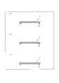
- (A)-(c) is sectional drawing which shows the shape of a projection part. In these drawings, a cross section taken along the line A-A ′ of the light guide shown in FIG. It is a side view which shows the other structural example of the backlight provided in the liquid crystal display device of this invention.
- Embodiments of the present invention will be described with reference to FIGS. 1 to 8 as follows. Note that the present invention is not limited to this.
- FIG. 2 shows a configuration of a liquid crystal display device 1 including a tandem illumination device as a backlight.
- the liquid crystal display device 1 includes a backlight 2 (illumination device) and a liquid crystal display panel 3 disposed to face the backlight 2.
- the liquid crystal display panel 3 is the same as a general liquid crystal display panel used in a conventional liquid crystal display device, and although not shown, for example, an active matrix substrate on which a plurality of TFTs (thin film transistors) are formed, and a liquid crystal display panel 3 is opposed thereto. And a liquid crystal layer sealed between the substrates by a sealing material.
- TFTs thin film transistors
- the configuration of the backlight 2 provided in the liquid crystal display device 1 will be described in detail below.
- the backlight 2 is arranged behind the liquid crystal display panel 3 (on the side opposite to the display surface).
- the backlight 2 includes a plurality of light emitting units 11, a diffusion plate 8, and an optical sheet 9.
- the light emitting unit 11 having one light guide 7 and the light emitting unit 11 having the other light guide 17 will be described as examples. Unless otherwise specified, one light guide 7 will be described as an example as a representative of both light guides 7 and 17.
- One light emitting unit 11 includes a light source 5, a light guide 7 that diffuses light from the light source 5 to emit light, a substrate 4 on which the light source 5 is disposed, a reflection sheet 6, and the like.
- the light guide 7 includes a light emitting part 7b having a light emitting surface 7a and a light guiding part 7c that guides light from the light source 5 to the light emitting part 7b, and at least a connection portion between the light emitting part 7b and the light guiding part 7c.
- the thicknesses of the light guides 7 are different from each other, and the light emitting part 17 b of the other light guide 17 is disposed on the light guide 7 c of the light guide 7.
- a plurality of light guides 7, 17,... Form a flush light emitting surface (light emitting surface of the entire backlight 2; light emitting region). Such an arrangement is called a tandem arrangement.
- the diffusion plate 8 and the optical sheet 9 are arranged in this order on the upper part of the structure in which the plurality of light emitting units 11 are arranged in tandem as shown in FIG.
- the diffusion plate 8 is disposed to face the light emitting surface 7a so as to cover the entire flush light emitting surface (light emitting region) formed by the light emitting surfaces 7a of the light guides 7, 17,.
- the diffusion plate 8 diffuses the light emitted from the light emitting surface 7 a of the light guide 7 and irradiates the optical sheet 9.
- the optical sheet 9 is composed of a plurality of sheets arranged on the front surface side of the light guide 7, uniformizes and collects light emitted from the light emitting surface 7 a of the light guide 7, and displays a liquid crystal display.
- the panel 3 is irradiated. That is, the optical sheet 9 reflects a diffusion sheet that collects and scatters light, a lens sheet that collects light and improves luminance in the front direction (the direction of the liquid crystal display panel), and reflects one polarization component of light. Then, a polarization reflection sheet or the like that improves the luminance of the liquid crystal display device 1 by transmitting the other polarization component can be applied. These are preferably used in appropriate combination depending on the price and performance of the liquid crystal display device 1.
- the configuration in which the diffusion plate 8 is directly placed on the light emitting surface 7a of the light guide 7 has been described as an example.
- the present invention is not limited to such a configuration.
- a transparent plate is disposed between the light guide 7 and the diffusion plate 8 can be cited.
- the transparent plate is formed of a translucent material such as a polyethylene film.
- the light emitted from the point light source 5 travels through the light guide 7 while receiving the scattering action and the reflection action, and is emitted from the light emitting surface 7a.
- the light emitted from the light emitting surface 7a is diffused by the diffusing sheet 8 and the optical sheet 9 to be uniformed and condensed and irradiated onto the liquid crystal display panel 3.
- FIG. 1 is a side view showing a partial configuration of a backlight 2 provided in the liquid crystal display device 1 shown in FIG. FIG. 1 shows a state where two light emitting units 11 are arranged in a tandem manner as a partial configuration of the backlight 2.
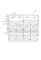
- FIG. 3 is a plan view showing a partial configuration of the backlight 2 provided in the liquid crystal display device 1 shown in FIG.
- the backlight 2 is formed by arranging a plurality of light emitting units 11 vertically and horizontally.
- FIG. 3 as a partial configuration of the backlight 2, a state in which four light emitting units 11 are arranged in two vertically and two horizontally is shown.
- the reflection sheet 6 is hatched.
- the reflection sheet 6 that is set with one light guide 7 and the reflection sheet 6 that is set with the other light guide 17 are the types of hatching. Is changing.
- FIGS. 1 and 3 the diffusion plate 8 and the optical sheet 9 are not shown.
- a protrusion 12 is provided on the back surface of the light guide 7 (the surface facing the reflection sheet 6). Further, the reflection sheet 6 is provided with a hole (hole) 14 into which the protrusion 12 is fitted at a position corresponding to the protrusion 12. Further, the substrate 4 is provided with through holes (holes) 13 into which the protrusions 12 are fitted at positions corresponding to the protrusions 12 and the holes 14.
- the light source 5 is fixedly disposed on the substrate 4 as described above, and the protrusion 12 of the light guide 7 is fitted to the reflection sheet 6 and the substrate 4.
- a hole 14 and a through hole 13 are provided.
- the light source 5 is a point light source such as a light emitting diode (LED).
- the light source 5 is composed of a plurality of types of light emitting diodes having different emission colors.
- the light source 5 is composed of an LED group in which a plurality of light emitting diodes of three colors of red (R), green (G), and blue (B) are arranged. By combining the light emitting diodes of these three colors to form a light source, white light can be irradiated on the light emitting surface.
- the light source does not necessarily need to be composed of a plurality of types having different emission colors.
- the light source may be composed of only one type of LED such as a white LED.
- the color combination of the light emitting diodes can be appropriately determined based on the color development characteristics of the LEDs of each color and the color development characteristics of the backlight desired according to the purpose of use of the liquid crystal display device 1.
- the light source 5 composed of this LED group is mounted on the substrate 4.
- a side light emitting type LED in which LED chips of respective colors are molded in one package may be used.
- a backlight having a wide color reproduction range can be obtained.
- the light source 5 having the above configuration is fixed and mounted on the substrate 4.
- FIG. 6A and 6B show a partial configuration of the substrate 4.
- FIG. 6A is a plan view of the substrate 4, and
- FIG. 6B is a side view of the substrate 4.
- a light source 5 is mounted on a substrate 4, and a through hole 13 for alignment is formed in the substrate 4.
- a driver (not shown) for controlling lighting of each LED constituting the light source 5 is mounted on the substrate 4. Since the driver is mounted on the same substrate 4 together with the light source 5, the number of substrates can be reduced, and connectors and the like connecting the substrates can be reduced, so that the cost of the apparatus can be reduced. Further, the backlight 2 can be thinned by reducing the number of substrates.
- one substrate 4 is provided for the plurality of light emitting units 11, 11, 11.
- the relative positioning of each light emitting unit 11 can be more accurately performed. Thereby, the brightness
- This configuration can also reduce the number of substrates.
- the light guide 7 causes the light emitted from the light source 5 to emit light from the light emitting surface 7a.
- the light emitting surface 7a is a surface for irradiating the irradiation target with light.
- the light guide 7 has a tandem structure as shown in FIGS. That is, the light guide 7 has a light emitting part 7b having a light emitting surface 7a and a light guiding part 7c that guides light from the light source 5 to the light emitting part 7b, and at least the light emitting part 7b and the light guiding part 7c.
- the thicknesses are different from each other, and the light emitting portion 17b of the other light guide 17 is disposed on the light guide 7c of the light guide 7.
- a plurality of light guides 7, 17,... Form a flush light emitting surface (light emitting surface of the entire backlight 2; light emitting region).
- FIG. 4A shows a planar configuration of the light guide 7.
- FIG. 4B is a side view of the light guide 7.
- two light source placement holes 15 are formed near the end of the light guide 7 on the light guide 7 c side.
- a protrusion 12 is provided on the back surface of the light guide 7 (surface opposite to the light emitting surface 7a).
- the protrusion 12 is provided on the light guide 7 c side of the light guide 7.
- the protrusion becomes an obstacle when the light guides are arranged in an overlapping manner, and the alignment of each light guide can be performed appropriately. There is a possibility of disappearing.
- the protrusions 12 are provided on the back surface of the light guide body 7 on the light guide section 7c side, so that the plurality of light guide bodies 7 (17) are tandem. When the layers are arranged in an overlapping manner, the light guides 7 (17) can be properly positioned on the substrate 4 without the protrusions 12 becoming an obstacle to the overlapping arrangement.
- the arrangement position of the protrusion 12 is indicated by a broken line.
- the protrusion 12 is provided near the end of the light guide 7 (in other words, closer to the end than the center of the light guide 7). Since the amount of light traveling in the light guide 7 is greater in the center than in the end of the light guide 7, the protrusion 12 is provided at a position close to the end of the light guide. The influence of the protrusion 12 on the light traveling in the light guide can be reduced.
- the protrusion 12 is provided in the region where the light beam is not sufficiently diffused at both ends of the light guide 7, that is, in the light guide 7 c of the light guide 7 at the end closer to the light source 5. More preferably.
- the present invention is not limited to this configuration.
- substrate 4 gave as an example the structure by which the through-hole 13 was formed as a member for alignment with the light guide 7 and the reflective sheet 6, this invention is given.
- the present invention is not limited to this, and the substrate 4 may be provided with a recess as an alignment member.
- the reflective sheet 6 may be provided with a recess into which the protrusion 12 is fitted.
- the protrusion 12 of the light guide 7 is fitted in the alignment hole or concave portion provided in the substrate 4 in a state of being in contact with the concave portion of the reflective sheet 6. Include. Therefore, the light that has entered the protrusion is also reflected by the action of the reflection sheet.
- the light guide 7 is mainly made of a transparent resin such as polycarbonate (PC) or polymethyl methacrylate (PMMA), but is not particularly limited, and is preferably made of a material having high light transmittance.
- the light guide 7 can be formed by, for example, injection molding, extrusion molding, hot press molding, cutting, or the like. However, it is not limited to these shaping
- FIGS. 7A and 7B show examples of the cross-sectional shape of the protruding portion 12.
- FIG. 4A the shape of the cross section along the line A-A ′ of the light guide 7 shown in FIG. 4A is shown.
- the protrusion 12 shown in FIGS. 7A and 7B is cylindrical, and the protrusion 12 shown in FIG. 7C is conical.
- the columnar protrusion 12 shown in FIG. 7 (a) has a higher column height than the columnar protrusion 12 shown in FIG. 7 (b). Thereby, it can be set as the structure which is hard to remove
- the conical protrusion 12 shown in FIG. 7C has an advantage that it is easy to fit in the through hole 13 formed in the substrate 4 compared to the columnar protrusion 12 because the tip is thin. There is.
- each shape of the above-mentioned projection part 12 is an example of this invention, and this invention is not limited to these.
- FIG. 5 shows a planar configuration of the reflection sheet 6. As shown in this figure, the reflection sheet 6 is provided with holes 14 at positions corresponding to the protrusions 12 provided on the light guide 7.
- the reflection sheet 6 is provided so as to be in contact with the back surface of the light guide 7 (the surface facing the light emitting surface 7a).
- the reflection sheet 6 reflects light and emits more light from the light emitting surface 7a.
- a plurality of light guides 7 are provided, and a reflection sheet 6 is provided for each of the light guides 7, 17,.
- the protrusion 12 is provided on the back surface of the light guide 7, and the reflection sheet 6 corresponds to the position of the protrusion 12.
- a hole 14 into which the projection 12 is fitted is formed, and a through hole 13 into which the projection 12 is fitted is formed in the substrate 4 on which the light source 5 is fixedly arranged.
- the positioning members are positioned so that the light guide 7, the reflection sheet 6, and the substrate 4 are arranged with a desired positional relationship.
- positioned can be accurately aligned and arrange
- two protrusions 12, through holes 13, and holes 14 are provided for each light emitting unit 11. As described above, since a plurality of positioning members are provided, the positions can be more accurately aligned.
- two protrusions 12, two through holes 13, and two holes 14 are provided as an example.
- the number of each is three or more, Good.
- one of the three protrusions provided on the light guide is the light emitting part of the light guide. It is preferable to be provided near the tip. Thereby, it can prevent that a brightness
- the provision of a large number of protrusions breaks down the conditions for total reflection of light and causes light to leak from the light guide. May be reduced. Therefore, when a large number of protrusions are provided, a coating is made on the surface other than the light emitting surface of the light guide so that light does not leak to the outside, so that light does not leak from other than the light emitting surface. A decrease in luminance efficiency due to the provision can be suppressed.
- Examples of the process for preventing the light from leaking to the outside include a mirror coating process.
- the mirror surface coating treatment is to finish the surface to a mirror surface by applying a predetermined coating agent to the surface.
- FIG. 8 shows another configuration example of the backlight according to the present invention.
- FIG. 8 is a side view showing a partial configuration of the backlight 52 provided in the liquid crystal display device of the present invention.
- FIG. 8 shows a state in which two light emitting units 61 are arranged by a tandem method as a partial configuration of the backlight 2.
- the backlight 52 is provided with a diffusion plate 8 and an optical sheet 9.
- the 8 includes a plurality of light emitting units 61.
- the light emitting unit 61 having one light guide 57 and the light emitting unit 61 having the other light guide 67 will be described as examples. Unless otherwise specified, one of the light guides 57 and 67 will be described as an example.
- One light emitting unit 61 includes a light source 55, a light guide 57 that diffuses light from the light source 55 to emit light, a substrate 54 on which the light source 55 is disposed, a reflection sheet 56, and the like.
- the light guide 57 includes a light emitting portion 57b having a light emitting surface 57a and a light guiding portion 57c that guides light from the light source 55 to the light emitting portion 57b, and at least a connection portion between the light emitting portion 57b and the light guiding portion 57c.
- the thicknesses of the light guides 57 are different from each other, and the light emitting part of the other light guide 67 is disposed on the light guide 57c of the light guide 57.
- a plurality of light guides 57, 67,... Form a flush light emitting surface (light emitting surface of the entire backlight 52; light emitting region).
- a protrusion 62 a is provided on the back surface of the light guide body 57 (the surface facing the reflection sheet 56). Further, the reflection sheet 56 is provided with a hole (hole) into which the projection 12 is fitted at a position corresponding to the projection 62a. Further, the substrate 54 is provided with through holes (holes) 63 into which the protrusions 62 a are fitted at positions corresponding to the protrusions 62 a and the holes of the reflection sheet 56.
- the backlight 52 includes an upper surface of the light guide portion 57 c of the light guide 57 (a surface opposite to the back surface of the light guide 57 and the same side as the light emitting surface 57 a).
- another protrusion 62b is provided on the surface) side.
- the protrusion part 62b is inserted in the hole provided in the reflective sheet 66 arrange
- an illuminating device with improved luminance uniformity can be realized.
- the illumination device of the present invention can be used as a backlight of a liquid crystal display device.
Landscapes
- Physics & Mathematics (AREA)
- General Physics & Mathematics (AREA)
- Optics & Photonics (AREA)
- Planar Illumination Modules (AREA)
Abstract
Description
2 バックライト(照明装置)
3 液晶表示パネル
4 基板
5 光源
6 反射シート
7 導光体
17 導光体
7a 発光面
7b 発光部
7c 導光部
11 発光ユニット
12 突起部
13 貫通孔(孔または凹部)
14 穴(孔)
52 バックライト(照明装置)
54 基板
55 光源
56 反射シート
57 導光体
67 導光体
57a 発光面
57b 発光部
57c 導光部
61 発光ユニット
62a 突起部
62b 突起部
63 貫通孔(孔または凹部)
66 反射シート
Claims (8)
- 光源、該光源からの光を拡散させて発光面から出射させる導光体、および、該導光体の発光面とは反対側に配置され、導光体内を進行する光を発光面の方へ反射させる反射シートを含む発光ユニットを複数個備え、
上記複数個の発光ユニットを構成する各導光体は、発光面を有する発光部と、該発光部へ上記光源からの光を導く導光部とを有し、一方の導光体の導光部に、該一方の導光体に隣り合う他方の導光体の発光部が乗り上げるようにして並んで配置されている照明装置であって、
上記光源を固定配置するための基板をさらに備え、
上記導光体には、上記反射シートとの対向面側に突起部が設けられているとともに、
上記反射シートおよび上記基板には、上記突起部と嵌合する孔または凹部が形成されていることを特徴とする照明装置。 - 上記基板は、複数の発光ユニットに対して1つ設けられていることを特徴とする請求項1に記載の照明装置。
- 上記突起部は、上記導光体の導光部に設けられていることを特徴とする請求項1または2に記載の照明装置。
- 上記突起部は、上記導光体の中央部よりも端部に近い位置に設けられていることを特徴とする請求項1~3の何れか1項に記載の照明装置。
- 上記突起部、および、上記孔または凹部は、複数個設けられていることを特徴とする請求項1~4の何れか1項に記載の照明装置。
- 上記導光体には、上記基板上に固定された上記光源が嵌り込む孔が形成されていることを特徴とする請求項1~5の何れか1項に記載の照明装置。
- 上記導光体の発光面以外の面には、鏡面コーティング処理が施されていることを特徴とする請求項1~6の何れか1項に記載の照明装置。
- 請求項1~7の何れか1項に記載の照明装置をバックライトとして備えていることを特徴とする液晶表示装置。
Priority Applications (2)
| Application Number | Priority Date | Filing Date | Title |
|---|---|---|---|
| CN2009801329526A CN102132083A (zh) | 2008-09-30 | 2009-06-24 | 照明装置和液晶显示装置 |
| US13/058,199 US20110141396A1 (en) | 2008-09-30 | 2009-06-24 | Illumination device and liquid crystal display device |
Applications Claiming Priority (2)
| Application Number | Priority Date | Filing Date | Title |
|---|---|---|---|
| JP2008-254399 | 2008-09-30 | ||
| JP2008254399 | 2008-09-30 |
Publications (1)
| Publication Number | Publication Date |
|---|---|
| WO2010038523A1 true WO2010038523A1 (ja) | 2010-04-08 |
Family
ID=42073300
Family Applications (1)
| Application Number | Title | Priority Date | Filing Date |
|---|---|---|---|
| PCT/JP2009/061516 Ceased WO2010038523A1 (ja) | 2008-09-30 | 2009-06-24 | 照明装置および液晶表示装置 |
Country Status (3)
| Country | Link |
|---|---|
| US (1) | US20110141396A1 (ja) |
| CN (1) | CN102132083A (ja) |
| WO (1) | WO2010038523A1 (ja) |
Families Citing this family (7)
| Publication number | Priority date | Publication date | Assignee | Title |
|---|---|---|---|---|
| WO2009017066A1 (ja) * | 2007-07-27 | 2009-02-05 | Sharp Kabushiki Kaisha | 照明装置、表示装置、並びに導光板 |
| CN102177393B (zh) * | 2008-10-31 | 2013-11-06 | 夏普株式会社 | 照明装置、显示装置和电视接收装置 |
| KR101676870B1 (ko) * | 2009-07-31 | 2016-11-16 | 엘지전자 주식회사 | 백라이트 유닛 및 그를 이용한 디스플레이 장치 |
| TWI448785B (zh) * | 2011-07-19 | 2014-08-11 | Innolux Corp | 多區域動態背光模組 |
| US8941795B2 (en) | 2011-12-20 | 2015-01-27 | Apple Inc. | Electronic device with backlit display |
| JP6167629B2 (ja) | 2013-04-12 | 2017-07-26 | 船井電機株式会社 | 表示装置 |
| CN106873240B (zh) * | 2017-02-07 | 2020-05-19 | 深圳市华星光电技术有限公司 | 背光组件及液晶显示模组 |
Citations (4)
| Publication number | Priority date | Publication date | Assignee | Title |
|---|---|---|---|---|
| JPS5953703U (ja) * | 1982-09-30 | 1984-04-09 | 日本精機株式会社 | 照明装置 |
| JP2001312916A (ja) * | 2000-02-24 | 2001-11-09 | Sony Corp | 面光源装置 |
| JP2002040423A (ja) * | 2000-07-31 | 2002-02-06 | Optrex Corp | 液晶表示素子の照明装置 |
| WO2008050509A1 (en) * | 2006-10-27 | 2008-05-02 | Sharp Kabushiki Kaisha | Light source device, backlight device, and liquid crystal display device |
Family Cites Families (1)
| Publication number | Priority date | Publication date | Assignee | Title |
|---|---|---|---|---|
| US7173677B2 (en) * | 2001-04-12 | 2007-02-06 | Rohm Co., Ltd. | Back light unit for liquid crystal display device and method for manufacturing the unit |
-
2009
- 2009-06-24 US US13/058,199 patent/US20110141396A1/en not_active Abandoned
- 2009-06-24 CN CN2009801329526A patent/CN102132083A/zh active Pending
- 2009-06-24 WO PCT/JP2009/061516 patent/WO2010038523A1/ja not_active Ceased
Patent Citations (4)
| Publication number | Priority date | Publication date | Assignee | Title |
|---|---|---|---|---|
| JPS5953703U (ja) * | 1982-09-30 | 1984-04-09 | 日本精機株式会社 | 照明装置 |
| JP2001312916A (ja) * | 2000-02-24 | 2001-11-09 | Sony Corp | 面光源装置 |
| JP2002040423A (ja) * | 2000-07-31 | 2002-02-06 | Optrex Corp | 液晶表示素子の照明装置 |
| WO2008050509A1 (en) * | 2006-10-27 | 2008-05-02 | Sharp Kabushiki Kaisha | Light source device, backlight device, and liquid crystal display device |
Also Published As
| Publication number | Publication date |
|---|---|
| CN102132083A (zh) | 2011-07-20 |
| US20110141396A1 (en) | 2011-06-16 |
Similar Documents
| Publication | Publication Date | Title |
|---|---|---|
| CN101680636B (zh) | 照明装置和液晶显示装置 | |
| CN101896765B (zh) | 照明装置和液晶显示装置 | |
| US8339539B2 (en) | Illumination device and liquid crystal display device | |
| CN101680637B (zh) | 照明装置和液晶显示装置 | |
| US20110164404A1 (en) | Illumination device, surface light source device, and liquid crystal display apparatus | |
| WO2010038523A1 (ja) | 照明装置および液晶表示装置 | |
| US20110109836A1 (en) | Illumination device and liquid crystal display device | |
| US8345188B2 (en) | Illumination device and liquid crystal display device | |
| JP5043198B2 (ja) | 照明装置および液晶表示装置 | |
| JP5189596B2 (ja) | 照明装置および液晶表示装置 | |
| US7796209B2 (en) | Illumination device and liquid crystal display device | |
| JPWO2010052955A1 (ja) | 面光源装置および液晶表示装置 | |
| US20110292684A1 (en) | Illumination device, surface illuminant device, and liquid crystal display device | |
| US8405796B2 (en) | Illumination device, surface light source device, and liquid crystal display device | |
| US20110109840A1 (en) | Light guide unit, surface light source device and liquid crystal display device | |
| US20110116006A1 (en) | Illumination device and liquid crystal display device | |
| HK1143850B (en) | Illuminating device and liquid crystal display device |
Legal Events
| Date | Code | Title | Description |
|---|---|---|---|
| WWE | Wipo information: entry into national phase |
Ref document number: 200980132952.6 Country of ref document: CN |
|
| 121 | Ep: the epo has been informed by wipo that ep was designated in this application |
Ref document number: 09817561 Country of ref document: EP Kind code of ref document: A1 |
|
| WWE | Wipo information: entry into national phase |
Ref document number: 13058199 Country of ref document: US |
|
| NENP | Non-entry into the national phase |
Ref country code: DE |
|
| 122 | Ep: pct application non-entry in european phase |
Ref document number: 09817561 Country of ref document: EP Kind code of ref document: A1 |
|
| NENP | Non-entry into the national phase |
Ref country code: JP |