WO2010023835A1 - 液晶素子及び光ピックアップ光学系 - Google Patents
液晶素子及び光ピックアップ光学系 Download PDFInfo
- Publication number
- WO2010023835A1 WO2010023835A1 PCT/JP2009/003880 JP2009003880W WO2010023835A1 WO 2010023835 A1 WO2010023835 A1 WO 2010023835A1 JP 2009003880 W JP2009003880 W JP 2009003880W WO 2010023835 A1 WO2010023835 A1 WO 2010023835A1
- Authority
- WO
- WIPO (PCT)
- Prior art keywords
- liquid crystal
- transparent electrode
- crystal element
- electrode layer
- phase difference
- Prior art date
- Legal status (The legal status is an assumption and is not a legal conclusion. Google has not performed a legal analysis and makes no representation as to the accuracy of the status listed.)
- Ceased
Links
Images

















Classifications
-
- G—PHYSICS
- G02—OPTICS
- G02F—OPTICAL DEVICES OR ARRANGEMENTS FOR THE CONTROL OF LIGHT BY MODIFICATION OF THE OPTICAL PROPERTIES OF THE MEDIA OF THE ELEMENTS INVOLVED THEREIN; NON-LINEAR OPTICS; FREQUENCY-CHANGING OF LIGHT; OPTICAL LOGIC ELEMENTS; OPTICAL ANALOGUE/DIGITAL CONVERTERS
- G02F1/00—Devices or arrangements for the control of the intensity, colour, phase, polarisation or direction of light arriving from an independent light source, e.g. switching, gating or modulating; Non-linear optics
- G02F1/29—Devices or arrangements for the control of the intensity, colour, phase, polarisation or direction of light arriving from an independent light source, e.g. switching, gating or modulating; Non-linear optics for the control of the position or the direction of light beams, i.e. deflection
-
- G—PHYSICS
- G11—INFORMATION STORAGE
- G11B—INFORMATION STORAGE BASED ON RELATIVE MOVEMENT BETWEEN RECORD CARRIER AND TRANSDUCER
- G11B7/00—Recording or reproducing by optical means, e.g. recording using a thermal beam of optical radiation by modifying optical properties or the physical structure, reproducing using an optical beam at lower power by sensing optical properties; Record carriers therefor
- G11B7/12—Heads, e.g. forming of the optical beam spot or modulation of the optical beam
- G11B7/135—Means for guiding the beam from the source to the record carrier or from the record carrier to the detector
- G11B7/1365—Separate or integrated refractive elements, e.g. wave plates
- G11B7/1369—Active plates, e.g. liquid crystal panels or electrostrictive elements
-
- G—PHYSICS
- G11—INFORMATION STORAGE
- G11B—INFORMATION STORAGE BASED ON RELATIVE MOVEMENT BETWEEN RECORD CARRIER AND TRANSDUCER
- G11B7/00—Recording or reproducing by optical means, e.g. recording using a thermal beam of optical radiation by modifying optical properties or the physical structure, reproducing using an optical beam at lower power by sensing optical properties; Record carriers therefor
- G11B7/12—Heads, e.g. forming of the optical beam spot or modulation of the optical beam
- G11B7/135—Means for guiding the beam from the source to the record carrier or from the record carrier to the detector
- G11B7/1392—Means for controlling the beam wavefront, e.g. for correction of aberration
- G11B7/13925—Means for controlling the beam wavefront, e.g. for correction of aberration active, e.g. controlled by electrical or mechanical means
-
- G—PHYSICS
- G02—OPTICS
- G02F—OPTICAL DEVICES OR ARRANGEMENTS FOR THE CONTROL OF LIGHT BY MODIFICATION OF THE OPTICAL PROPERTIES OF THE MEDIA OF THE ELEMENTS INVOLVED THEREIN; NON-LINEAR OPTICS; FREQUENCY-CHANGING OF LIGHT; OPTICAL LOGIC ELEMENTS; OPTICAL ANALOGUE/DIGITAL CONVERTERS
- G02F1/00—Devices or arrangements for the control of the intensity, colour, phase, polarisation or direction of light arriving from an independent light source, e.g. switching, gating or modulating; Non-linear optics
- G02F1/29—Devices or arrangements for the control of the intensity, colour, phase, polarisation or direction of light arriving from an independent light source, e.g. switching, gating or modulating; Non-linear optics for the control of the position or the direction of light beams, i.e. deflection
- G02F1/291—Two-dimensional analogue deflection
-
- G—PHYSICS
- G11—INFORMATION STORAGE
- G11B—INFORMATION STORAGE BASED ON RELATIVE MOVEMENT BETWEEN RECORD CARRIER AND TRANSDUCER
- G11B7/00—Recording or reproducing by optical means, e.g. recording using a thermal beam of optical radiation by modifying optical properties or the physical structure, reproducing using an optical beam at lower power by sensing optical properties; Record carriers therefor
- G11B2007/0003—Recording, reproducing or erasing systems characterised by the structure or type of the carrier
- G11B2007/0009—Recording, reproducing or erasing systems characterised by the structure or type of the carrier for carriers having data stored in three dimensions, e.g. volume storage
- G11B2007/0013—Recording, reproducing or erasing systems characterised by the structure or type of the carrier for carriers having data stored in three dimensions, e.g. volume storage for carriers having multiple discrete layers
Definitions
- the present invention relates to a liquid crystal element and an optical pickup optical system.
- the NA of the BD is 0.85, and the NA of a DVD (Digital Versatile Disc) is 0.65. Therefore, the spherical aberration generated when recording / reproducing BD is likely to increase as compared with a conventional optical disk such as DVD. Therefore, in an optical pickup optical system that records and reproduces BD, a correction mechanism that reduces spherical aberration based on the difference in substrate thickness of each recording layer is essential.
- Patent Document 1 describes a technique for moving the position of a collimator lens disposed between a light source and an objective lens in order to change the imaging magnification of the objective lens.
- DVD and CD Compact Disc
- Japanese Patent Application Laid-Open No. 2004-228561 describes a technique for moving each lens in the optical pickup optical system and changing the interval between the lenses. Thereby, the spherical aberration based on the difference in the substrate thickness of each recording layer in the two-layer optical recording medium is reduced.
- Patent Document 3 describes a technique in which an objective lens and a liquid crystal element are mounted on an actuator, and the objective lens and the liquid crystal element are integrally moved. This prevents aberration deterioration due to axial misalignment associated with tracking. Also described is a technique for reducing the number of elastic supports connected to the actuator by superimposing the liquid crystal element drive signal and the actuator drive signal.
- Patent Document 4 describes a technology in which a semiconductor element that drives a liquid crystal element is mounted on an actuator, and only a drive signal that drives the semiconductor element is conducted through an elastic support of the actuator. This further reduces the number of elastic supports.
- Patent Document 5 discloses a liquid crystal element that corrects spherical aberration based on the difference in substrate thickness of each recording layer, and a liquid crystal element that corrects spherical aberration based on variations in the substrate thickness of the recording layer of each optical recording medium. An optical pickup optical system is described.
- Patent Document 6 describes an optical pickup optical system including a liquid crystal element including two transparent substrates and a liquid crystal layer sandwiched between the two transparent substrates.
- a blaze grating is provided on the liquid crystal layer side of one transparent substrate.
- Each of the two transparent substrates is provided with a transparent electrode layer in which a plurality of transparent electrodes of different sizes formed in an annular shape are arranged concentrically with the optical axis as a concentricity.
- the spherical aberration based on the difference in the substrate thickness of each recording layer is corrected, and the voltage is applied to the transparent electrode layer of the other transparent substrate.
- spherical aberration based on variations in the substrate thickness of the recording layer of each optical recording medium is corrected.
- Patent Document 7 describes a liquid crystal element having a liquid crystal layer sandwiched between two transparent substrates. Then, the first transparent electrode layer for correcting the spherical aberration based on the difference in the substrate thickness of each recording layer is provided on one transparent substrate, and the substrate thickness of the recording layer of each optical recording medium varies on the other transparent substrate. A second transparent electrode layer for correcting spherical aberration based on the above is provided. The first transparent electrode layer and the second transparent electrode layer are formed by concentrically arranging a plurality of transparent electrodes formed in a ring shape and having different sizes.
- the fact that the phase difference is an integral multiple of the wavelength is the same as the case where there is no phase difference, thereby reducing the phase difference generated by applying a voltage to the first transparent electrode layer.
- a phase difference that is an integral multiple of the wavelength is subtracted from the phase difference required to correct spherical aberration based on the difference in substrate thickness of each recording layer. The phase difference is generated. Thereby, the thickness of the liquid crystal layer is reduced.
- Patent Documents 1 and 2 have a problem that the optical pickup optical system becomes large because a mechanism for driving the lens is required. Moreover, in patent document 3 and 4, since a liquid crystal element is mounted in an actuator, there exists a problem that an actuator will become large sized. Further, since the weight of the actuator increases, the frequency response performance of the actuator deteriorates. Therefore, there is a problem that it becomes an obstacle to high-speed signal reproduction. Further, in Patent Document 5, since two liquid crystal elements are required, there are problems that an increase in the number of parts, an increase in size of the apparatus, and an increase in cost are caused.
- Patent Document 6 it is necessary to match the position of the transparent electrode provided on one transparent substrate with the position of the transparent electrode provided on the other transparent substrate in the radial direction. Therefore, there is a problem that the degree of freedom of aberration correction is reduced.
- the transparent electrode layer that provides a phase difference for correcting spherical aberration based on the difference in substrate thickness of each recording layer The ring width of each transparent electrode becomes wider.
- the annular width of each transparent electrode of the transparent electrode layer that gives a phase difference for correcting spherical aberration based on the variation in the substrate thickness of the recording layer of each optical recording medium is widened, and a continuous phase component is generated. It cannot be generated.
- the range of substrate thickness variations that can be corrected may be about 0.075 ⁇ 0.005 mm and 0.1 ⁇ 0.005 mm. In this case, it is not possible to correct various aberrations based on variations in the wavelength of the emitted light beam of the laser light source, variations in the objective lens, changes in spherical aberration due to temperature changes, and the like.
- Patent Document 7 the number of transparent electrodes of the first transparent electrode layer for correcting spherical aberration based on the difference in substrate thickness of each recording layer is large, and it is necessary to apply different voltages to the transparent electrodes. For this reason, the number of lead electrodes from each transparent electrode increases, and the proportion of the lead electrode wiring portion on the surface of the liquid crystal element increases. Therefore, there is a problem that a large aberration occurs in the wiring portion of the extraction electrode.
- the present invention has been made to solve such problems, and an object thereof is to provide a liquid crystal element and an optical pickup optical system capable of correcting large aberrations substantially continuously.
- the liquid crystal element according to the present invention is sandwiched between a first transparent substrate, a second transparent substrate facing the first transparent substrate, and the first transparent substrate and the second transparent substrate. And a refractive index anisotropic medium layer. Further, the liquid crystal element includes a first transparent substrate in which a plurality of first transparent electrodes of different sizes formed in a substantially ring shape are arranged concentrically around the optical axis. A second transparent electrode in which a transparent electrode layer and a plurality of second transparent electrodes having different sizes formed in a substantially ring shape are arranged concentrically around the optical axis on the second transparent substrate. And a layer.
- the first transparent electrode for applying a voltage having substantially the same value is disposed approximately periodically in the radial direction of the first transparent substrate.
- the refractive index anisotropic medium layer has a light flux transmitted through the liquid crystal element in a range of ⁇ h ⁇ to + h ⁇ (h is an integer satisfying h ⁇ 1; ⁇ is a design wavelength), and provides a phase difference that changes substantially periodically along the radial direction of the light beam, and a portion that provides a phase difference of h ⁇ between the light beams that pass through the adjacent first transparent electrodes.
- a voltage is applied to the refractive index anisotropic medium layer.
- the second transparent electrode layer may be configured such that the refractive index anisotropic medium layer imparts a phase difference that changes substantially continuously along a radial direction of the light beam to the light beam transmitted through the liquid crystal element.
- a voltage is applied to the refractive index anisotropic medium layer.
- the first transparent electrode for applying substantially the same voltage is disposed approximately periodically in the radial direction of the first transparent substrate.
- the refractive index anisotropic medium layer causes the light beam transmitted through the liquid crystal element to travel in the radial direction of the light beam within a range of ⁇ h ⁇ to + h ⁇ .
- a phase difference that changes substantially periodically along the axis is given.
- the liquid crystal element can give a large phase difference of ⁇ 1 ⁇ or less and + 1 ⁇ or more to the light beam transmitted through the liquid crystal element.
- phase difference is an integral multiple of the wavelength is the same as no phase difference
- a large phase difference of ⁇ 1 ⁇ or less and + 1 ⁇ or more is a phase difference of an integral multiple of the wavelength from the phase difference. Is equivalent to subtracting. If a phase difference of an integral multiple of the wavelength is subtracted from a large phase difference of ⁇ 1 ⁇ or less and + 1 ⁇ or more, a phase difference that changes substantially periodically along the radial direction of the light beam within a range of ⁇ 1 ⁇ or more and + 1 ⁇ or less is obtained. .
- h 1 ⁇ or less
- the refractive index anisotropic medium layer has a portion that imparts a phase difference of h ⁇ between light beams that pass through the adjacent first transparent electrodes.
- the refractive index anisotropic medium layer to which a voltage is applied by the first transparent electrode layer can generate defocus aberration in the light beam by applying such a phase difference to the light beam. Then, spherical aberration can be corrected by the defocus aberration.
- the defocus aberration is based on a large phase difference of ⁇ 1 ⁇ or less and + 1 ⁇ or more. Therefore, the defocus aberration amount is a large value. Accordingly, by applying a voltage to the refractive index anisotropic medium layer by the first transparent electrode layer, a relatively limited phase difference within a range of ⁇ h ⁇ or more and + h ⁇ or less is applied to the light beam transmitted through the liquid crystal element. By simply adding, a large defocus aberration based on a large phase difference of ⁇ 1 ⁇ or less and + 1 ⁇ or more can be generated, and a large spherical aberration can be corrected.
- the defocus aberration generated in the light beam transmitted through the liquid crystal element becomes a discrete value. Therefore, in the present invention, when the voltage is applied by the second transparent electrode layer, the refractive index anisotropic medium layer substantially continuously transmits the light beam transmitted through the liquid crystal element along the radial direction of the light beam. A changing phase difference is given. Accordingly, it is possible to generate an aberration having a substantially continuous value within a predetermined range in the light beam transmitted through the liquid crystal element.
- the refractive index anisotropic medium layer imparts discrete defocus aberration to the light beam transmitted through the liquid crystal element, and the substantially continuous value. Combined with defocus aberration. Therefore, when a voltage is applied by the first transparent electrode layer and the second transparent electrode layer, the refractive index anisotropic medium layer has a large phase difference of ⁇ 1 ⁇ or less and + 1 ⁇ or more to the light beam transmitted through the liquid crystal element. Therefore, it is possible to generate a substantially continuous defocus aberration. As a result, the liquid crystal element can correct large aberrations substantially continuously.
- the range of spherical aberration to be corrected by causing the liquid crystal element to generate aberration in a light beam transmitted through the liquid crystal element is ⁇ S or more and + S or less (S is a positive number)
- the refractive index anisotropic medium layer transmits a light beam transmitted through the liquid crystal element,-(i / j) S (where j is an odd number, i is an even number satisfying i ⁇ j, j I is an odd number satisfying i ⁇ j), 0, + (i / j) in the refractive index anisotropic medium layer so as to generate an aberration that corrects the amount of spherical aberration. It is preferable to apply a voltage.
- the refractive index anisotropic medium layer is within a range of ⁇ (1 / j) S or more and + (1 / j) S or less to a light beam transmitted through the liquid crystal element. It is preferable to apply a voltage to the refractive index anisotropic medium layer so as to generate an aberration that corrects the spherical aberration amount having a substantially continuous value.
- the range of the spherical aberration amount to be corrected by the aberration generated in the light beam transmitted through the liquid crystal element is equally divided by an arbitrary number 2j, and the first transparent electrode layer is driven, whereby the refractive index anisotropic medium is obtained.
- the layer generates a defocus aberration in the luminous flux so as to correct a discrete spherical aberration amount (-(i / j) S, 0, + (i / j) S) obtained by equally dividing the layer. .
- an aberration can be generated in the light beam so as to substantially continuously correct a spherical aberration amount of ⁇ S or more and + S or less.
- the range of aberrations generated in the light flux can be reduced by driving the second transparent electrode layer. Therefore, by increasing the number of j, the number of ring zones of the second transparent electrode of the second transparent electrode layer can be reduced.
- the liquid crystal element is fixedly disposed at a predetermined position of an optical pickup optical system for condensing the light beam from the laser light source on the optical recording medium, and the liquid crystal element is applied to the light beam transmitted through the liquid crystal element.
- the phase difference preferably includes a defocus component.
- the liquid crystal element in order to correct the spherical aberration based on the difference in the substrate thickness of each recording layer of the optical recording medium, the liquid crystal element generates a spherical aberration proportional to the fourth power of the ray height in the light beam transmitted through the liquid crystal element. .
- a large coma aberration proportional to the cube of the ray height occurs.
- the aberration generated in the light beam is the first power of the light beam height. Only the tilt component proportional to is left.
- the tilt component does not affect the spot shape of the light beam. Therefore, by including a defocus component in the phase difference that the liquid crystal element gives to the light beam that passes through the liquid crystal element, coma aberration due to axial misalignment or the like can be reduced.
- the weight of the actuator can be reduced as compared with the case where the liquid crystal element is mounted on the actuator together with the objective lens. Thereby, it is not necessary to degrade the frequency response of the actuator. Therefore, high-speed signal reproduction can be realized.
- the first transparent electrode layer has a plurality of the first transparent electrodes to which different voltages are applied, and the first transparent electrode has a plurality of annular zones to which the same voltage is applied.
- the transparent electrode in the annular zone has an end part in which a part thereof is deleted, the end of the transparent electrode in the inner annular zone, and the transparent electrode in the inner annular zone,
- the ends of the outer ring-shaped transparent electrodes to which the same voltage is applied are sequentially connected by the extraction electrodes along the substantially radial direction so that the extraction electrodes of the plurality of first transparent electrodes do not overlap each other. It is preferable to arrange
- the several ring-shaped electrode which applies the same voltage can be used as one 1st transparent electrode.
- the number of extraction electrodes can be set to the number of voltages applied to the first transparent electrode. Therefore, the area of the extraction electrode can be minimized, and the deterioration of the aberration correction performance of the liquid crystal element can be prevented.
- the number of ring zones of the second transparent electrode provided in the second transparent electrode layer may be smaller than the number of ring zones of the first transparent electrode provided in the first transparent electrode layer.
- a plurality of ring-shaped electrodes to which the same voltage is applied can be used as one first transparent electrode, but in the second transparent electrode layer, a ring-shaped electrode to which the same voltage is applied. Since the number of electrodes is small, it is difficult to reduce the number of extraction electrodes. Therefore, by increasing the number of ring zones of the first transparent electrode of the first transparent electrode layer more than the number of ring zones of the second transparent electrode provided in the second transparent electrode layer, the second transparent electrode layer The number of lead electrodes provided can be reduced. As a result, residual aberration can be reduced while improving the light utilization efficiency.
- liquid crystal element for an optical pickup optical system that condenses a light beam from a laser light source on an optical recording medium. Thereby, a large aberration generated in the optical pickup optical system can be corrected substantially continuously.
- an objective lens for condensing the light beam from the laser light source on the optical recording medium is provided, and the objective lens is a plastic lens.
- a plastic lens has a larger refractive index change due to a temperature change than a glass lens. Therefore, the change in spherical aberration is large. Further, in order to correct the spherical aberration that increases due to temperature change, when an annular structure is provided in the objective lens, spherical aberration based on wavelength change tends to increase. Therefore, when using a plastic objective lens, it is necessary to correct large spherical aberration.
- the large spherical aberration in the optical pickup optical system using the plastic objective lens can be corrected.
- the weight can be reduced, and the responsiveness of the actuator can be increased. Further, by making the objective lens made of plastic, the cost of the objective lens can be reduced.
- FIG. 1 is a side view schematically showing an example of an optical pickup optical system according to Example 1.
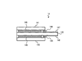
- FIG. 1 is a cross-sectional view schematically showing an example of a liquid crystal element according to Example 1.
- FIG. FIG. 6 is a plan view showing the arrangement of transparent electrodes in the first transparent electrode layer and the fourth transparent electrode layer of the liquid crystal element according to Example 1;
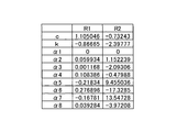
- 3 is a table showing an aspherical coefficient, a conic coefficient, and a curvature of the objective lens according to Example 1;
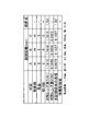
- 3 is a table showing the inter-surface distance and the refractive index of the optical pickup optical system according to Example 1.
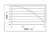
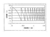
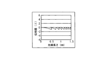
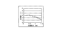
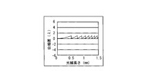
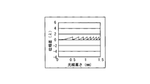
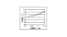
- Spherical aberration proportional to the cube of the ray height (r) generated by the difference in the substrate thickness of the recording layer, and coma aberration proportional to the cube of the ray height (r) generated by the axial deviation of 0.3 mm 3 is a graph showing a phase difference generated in a laser beam in a conventional liquid crystal element in order to reduce the noise. It is a graph which shows the phase difference obtained by subtracting the phase difference of the integral multiple of a wavelength from the phase difference shown in FIG. It is sectional drawing which shows the conventional liquid crystal element typically. It is sectional drawing which shows the conventional liquid crystal element typically. It is sectional drawing which shows the conventional liquid crystal element typically. It is sectional drawing which shows the conventional liquid crystal element typically. It is sectional drawing which shows the conventional liquid crystal element typically.
- FIG. It is a figure explaining spherical aberration corrected by generating aberration to laser light with the liquid crystal element concerning Example 1.
- FIG. It is a graph which shows an example of the phase difference given to the laser beam which permeate
- 6 is a graph showing an example of a phase difference imparted to laser light in the entire liquid crystal element according to Example 1.
- 6 is a graph showing an example of a phase difference imparted to laser light in the entire liquid crystal element according to Example 1. It is a graph which shows an example of the phase difference given to the laser beam which permeate
- 6 is a graph showing an example of a phase difference imparted to laser light in the entire liquid crystal element according to Example 1. It is a graph which shows an example of the phase difference given to the laser beam which permeate
- 6 is a graph showing an example of a phase difference imparted to laser light in the entire liquid crystal element according to Example 1. It is a graph which shows an example of the phase difference given to the laser beam which permeate
- 6 is a graph showing an example of a phase difference imparted to laser light in the entire liquid crystal element according to Example 1. It is a graph which shows an example of the phase difference given to the laser beam which permeate
- spherical aberration amount A the spherical aberration amount B, and the total spherical aberration amount (spherical aberration amount A + spherical aberration amount B) that are corrected by generating aberration in the laser light.
- the substrate thickness of the recording layer the value of coma aberration (COMA3), and the figure number.
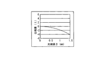
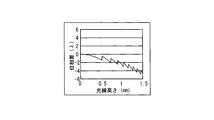
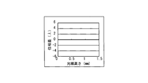
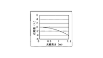
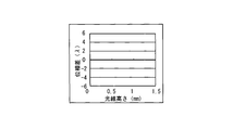
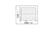
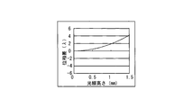
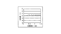
- 3 is a graph showing a phase difference actually given to laser light by the liquid crystal element according to Example 1; 3 is a graph showing a phase difference actually given to laser light by the liquid crystal element according to Example 1; 3 is a graph showing a phase difference actually given to laser light by the liquid crystal element according to Example 1; 3 is a graph showing a phase difference actually given to laser light by the liquid crystal element according to Example 1;
- the present invention is not limited to the following embodiments.
- the spherical aberration amount will be described by taking, as an example, spherical aberration caused by a difference in substrate thickness or variation of each recording layer of the optical recording medium.
- the variation of the laser diode, the objective lens It is also possible to correct the amount of spherical aberration caused by variations, temperature changes, and the like.
- FIG. 1 shows an example of an optical pickup optical system 1 according to the first embodiment.
- the optical pickup optical system 1 includes a laser diode 11 (laser light source), a polarization beam splitter (PBS) 12, a collimator lens 13, a liquid crystal element 14, a liquid crystal control circuit 15, a quarter wavelength plate 16, an objective lens 17, and a photodetector (PD). ) 18 etc.
- PBS polarization beam splitter
- PD photodetector
- a polarization beam splitter 12 is provided on the optical path of linearly polarized laser light (light beam) emitted from the laser diode 11.
- a collimator lens 13 is provided on the optical path of the laser light emitted from the polarization beam splitter 12. The collimator lens 13 converts the laser light emitted from the polarization beam splitter 12 from divergent light to substantially parallel light.
- a liquid crystal element is provided on the optical path of the laser light emitted from the collimator lens 13.
- a side view of the liquid crystal element 14 is shown in FIG.
- the liquid crystal element 14 includes a first transparent substrate 141 (first transparent substrate), a second transparent substrate 142 (second transparent substrate), and a third transparent substrate 143 (first transparent substrate).
- Transparent substrate first liquid crystal layer 144 (refractive index anisotropic medium layer), second liquid crystal layer 145 (refractive index anisotropic medium layer), and first transparent electrode layer 146 (first transparent electrode layer).
- the liquid crystal element 14 corrects the aberration of linearly polarized laser light.
- the first transparent electrode layer 146, the second transparent electrode layer 147, the third transparent electrode layer 148 and the fourth transparent electrode layer 149 of the liquid crystal element 14 are connected to the liquid crystal control circuit 15. Then, the liquid crystal control circuit 15 drives the first transparent electrode layer 146, the second transparent electrode layer 147, the third transparent electrode layer 148, and the fourth transparent electrode layer 149, whereby the liquid crystal element 14 is A phase difference is generated in the transmitted laser beam to correct the aberration.
- the liquid crystal element 14 corrects aberration by generating a phase difference in the laser light emitted from the collimator lens 13.
- the liquid crystal element 14 corrects aberration by generating a phase difference in the laser light reflected by the optical disk 19 (optical recording medium) and collected by the objective lens 17.
- first liquid crystal layer 144 and the second liquid crystal layer 145 are provided so that the alignment directions of the liquid crystal molecules are orthogonal to each other. Therefore, when the first liquid crystal layer 144 corrects the aberration of the laser light traveling from the laser diode 11 to the objective lens 17, the second liquid crystal layer 145 corrects the aberration of the laser light traveling from the optical disk 19 to the photodetector 18.
- a quarter-wave plate 16 is provided on the optical path of the laser light emitted from the liquid crystal element 14.
- the laser light emitted from the liquid crystal element 14 is converted into circularly polarized light by passing through the quarter-wave plate 16.
- the objective lens 17 is provided on the optical path of the laser beam that has passed through the quarter-wave plate 16.
- the objective lens 17 has a function of condensing incident laser light on the information recording surface of the optical disc 19 (optical recording medium).
- the objective lens 17 further has a function of guiding the laser beam reflected by the information recording surface of the optical disc 19 to the photodetector 18.
- the objective lens 17 is operated by an actuator (not shown).
- the objective lens 17 according to the example 1 converges the laser beam well on the recording layer having a substrate thickness of 0.0875 mm.
- the laser light emitted from the laser diode 11 passes through the polarization beam splitter 12 and enters the collimator lens 13.
- the collimator lens 13 converts the laser light emitted from the laser diode 11 from divergent light into substantially parallel light.
- the laser beam that has passed through the collimator lens 13 is incident on the liquid crystal element 14.
- the liquid crystal element 14 gives a phase difference that reduces aberration to the laser light transmitted through the liquid crystal element 14.
- the laser light that has passed through the liquid crystal element 14 passes through the quarter-wave plate 16 and then enters the objective lens 17. Then, the objective lens 17 focuses the laser beam on the information recording surface of the optical disc 19.
- the laser beam reflected by the information recording surface of the optical disc 19 enters the photodetector 18 through the objective lens 17 and is detected.
- the photodetector 18 detects the laser beam, performs photoelectric conversion, and outputs an output signal. Then, based on the output signal of the photodetector 18, a focus error signal, a track error signal, a reproduction signal, etc. are generated. Further, recording and / or reproduction of the optical disk 19 is performed using the focus error signal, track error signal, reproduction signal, and the like.
- the first transparent electrode layer 146 is formed on the surface of the first transparent substrate 141 on the first liquid crystal layer 144 side.
- the first transparent electrode layer 146 has a plurality of transparent electrodes (first transparent electrodes) formed in a substantially ring shape and having different sizes.
- the plurality of transparent electrodes are concentrically arranged on the first transparent substrate 141 around the optical axis of the liquid crystal element 14.
- the second transparent electrode layer 147 is formed on the surface of the second transparent substrate 142 on the first liquid crystal layer 144 side.
- the second transparent electrode layer 147 has a plurality of transparent electrodes (second transparent electrodes) formed in a substantially ring-shaped shape and having different sizes.
- the plurality of transparent electrodes are concentrically arranged on the second transparent substrate 142 with the optical axis of the liquid crystal element 14 as the center.
- the third transparent electrode layer 148 is formed on the surface of the second transparent substrate 142 on the second liquid crystal layer 145 side.
- the third transparent electrode layer 148 has a plurality of transparent electrodes (second transparent electrodes) formed in a substantially ring-shaped shape and having different sizes.
- the plurality of transparent electrodes are concentrically arranged on the second transparent substrate 142 with the optical axis of the liquid crystal element 14 as the center.
- the fourth transparent electrode layer 149 is formed on the surface of the third transparent substrate 143 on the second liquid crystal layer 145 side.
- the fourth transparent electrode layer 149 has a plurality of transparent electrodes (first transparent electrodes) formed in a substantially ring shape and having different sizes.
- the plurality of transparent electrodes are concentrically arranged on the third transparent substrate 143 with the optical axis of the liquid crystal element 14 as the center.
- the first transparent electrode layer 146 includes a first liquid crystal layer 144 that has a laser beam transmitted through the liquid crystal element 14 within the range of ⁇ h ⁇ to + h ⁇ (h is an integer that satisfies h ⁇ 1, Is a design wavelength), and a voltage is applied to the first liquid crystal layer 144 so as to give a phase difference that changes substantially periodically along the radial direction of the laser beam.
- the first liquid crystal layer 144 allows the laser light transmitted through the liquid crystal element 14 to emit laser light within a range of ⁇ h ⁇ to + h ⁇ .
- the first transparent electrode layer 146 has a portion in which the first liquid crystal layer 144 provides a phase difference of h ⁇ between laser beams that pass through adjacent transparent electrodes in the first transparent electrode layer 146.
- a voltage is applied to the first liquid crystal layer 144.
- the first liquid crystal layer 144 -(I / j) S (if j is an odd number, i is an even number satisfying i ⁇ j, and j is an even number, i is an odd number satisfying i ⁇ j).
- An aberration for correcting the spherical aberration amount of 0, + (i / j) S is generated.
- the first transparent electrode layer 146 has a spherical surface of ⁇ (i / j) S, 0, + (i / j) S to the laser light that the first liquid crystal layer 144 transmits through the liquid crystal element 14.
- a voltage is applied to the first liquid crystal layer 144 so as to generate an aberration that corrects the amount of aberration.
- the first liquid crystal layer 144 gives the laser light transmitted through the liquid crystal element 14 a phase difference that changes substantially periodically along the radial direction of the laser light within a range of ⁇ h ⁇ or more and + h ⁇ or less.
- the second transparent electrode layer 147 gives the first liquid crystal layer 144 a phase difference that changes substantially continuously along the radial direction of the laser light to the laser light transmitted through the liquid crystal element 14.
- a voltage is applied to the first liquid crystal layer 144.
- the first liquid crystal layer 144 imparts a phase difference that changes substantially continuously along the radial direction of the laser light to the laser light transmitted through the liquid crystal element 14, so that ⁇ (1 / J)
- An aberration for correcting the spherical aberration amount having a substantially continuous value within a range of S to + (1 / j) S is generated.
- the third transparent electrode layer 148 also causes the second liquid crystal layer 145 to give the laser beam transmitted through the liquid crystal element 14 a phase difference that changes substantially continuously along the radial direction of the laser beam.
- a voltage is applied to the second liquid crystal layer 145. Accordingly, when the range of the spherical aberration amount that is corrected by causing the liquid crystal element 14 to generate aberration in the laser light transmitted through the liquid crystal element 14 is ⁇ S or more and + S or less, the second liquid crystal layer 145 has the liquid crystal In the laser beam that passes through the element 14, an aberration that corrects the spherical aberration amount having a substantially continuous value within a range of ⁇ (1 / j) S or more and + (1 / j) S or less is generated.
- the second liquid crystal layer 145 imparts a phase difference that changes substantially continuously along the radial direction of the laser light to the laser light transmitted through the liquid crystal element 14, so that ⁇ (1 / J)
- An aberration for correcting the spherical aberration amount having a substantially continuous value within a range of S to + (1 / j) S is generated.
- the fourth transparent electrode layer 149 includes a second liquid crystal layer 145 in which laser light transmitted through the liquid crystal element 14 falls within a range of ⁇ h ⁇ to + h ⁇ (h is an integer satisfying h ⁇ 1, ⁇ Is a design wavelength), and a voltage is applied to the second liquid crystal layer 145 so as to give a phase difference that changes substantially periodically along the radial direction of the laser beam.
- the second liquid crystal layer 145 allows the laser light transmitted through the liquid crystal element 14 to emit laser light within a range of ⁇ h ⁇ or more and + h ⁇ or less. A phase difference that changes substantially periodically along the radial direction is applied. Further, the fourth transparent electrode layer 149 has a portion in which the second liquid crystal layer 145 gives a phase difference of h ⁇ between laser beams that pass through adjacent transparent electrodes in the fourth transparent electrode layer 149. A voltage is applied to the second liquid crystal layer 145.
- the second liquid crystal layer 145 has the liquid crystal An aberration that corrects the amount of spherical aberration of ⁇ (i / j) S, 0, + (i / j) S is generated in the laser light transmitted through the element 14.
- the fourth transparent electrode layer 149 has a spherical surface of ⁇ (i / j) S, 0, + (i / j) S in the laser beam transmitted from the second liquid crystal layer 145 through the liquid crystal element 14.
- a voltage is applied to the second liquid crystal layer 145 so as to generate an aberration for correcting the aberration amount.
- the second liquid crystal layer 145 gives the laser light transmitted through the liquid crystal element 14 a phase difference that changes approximately periodically along the radial direction of the laser light within a range of ⁇ h ⁇ or more and + h ⁇ or less.
- the laser beam can have ⁇ (i / j) S, 0, + (I / j) An aberration for correcting the spherical aberration amount of S is generated.
- the first transparent electrode layer 146 and the fourth transparent electrode layer 149 transparent electrodes that apply substantially the same voltage are periodically arranged in the radial direction of the first transparent substrate 141. Then, when a voltage is applied by the first transparent electrode layer 146 or the fourth transparent electrode layer 149, the first liquid crystal layer 144 or the second liquid crystal layer 145 changes the laser light transmitted through the liquid crystal element 14 into laser light. , A phase difference that changes substantially periodically along the radial direction of the laser beam is applied within a range of ⁇ h ⁇ to + h ⁇ . Thereby, the liquid crystal element 14 can give a large phase difference of ⁇ 1 ⁇ or less and + 1 ⁇ or more to the laser light transmitted through the liquid crystal element 14.
- phase difference is an integral multiple of the wavelength is the same as no phase difference
- a large phase difference of ⁇ 1 ⁇ or less and + 1 ⁇ or more is a phase difference of an integral multiple of the wavelength from the phase difference. Is equivalent to subtracting.
- a phase difference of an integral multiple of the wavelength is subtracted from a large phase difference of ⁇ 1 ⁇ or less and + 1 ⁇ or more, a phase difference that changes substantially periodically along the radial direction of the laser beam within a range of ⁇ 1 ⁇ or more and + 1 ⁇ or less. Become.
- h 1 ⁇
- a large phase difference of ⁇ 1 ⁇ or less and + 1 ⁇ or more can be imparted to the laser light.
- the first transparent electrode layer 146 or the fourth transparent electrode layer 149 when a voltage is applied by the first transparent electrode layer 146 or the fourth transparent electrode layer 149, the first liquid crystal layer 144 or the second liquid crystal layer 145 becomes the first transparent electrode layer 146 or the second transparent electrode layer 145.
- the fourth transparent electrode layer 149 has a portion that imparts a phase difference of h ⁇ between laser beams that pass through adjacent transparent electrodes.
- the first liquid crystal layer 144 or the second liquid crystal layer 145 to which a voltage is applied by the first transparent electrode layer 146 or the fourth transparent electrode layer 149 imparts such a phase difference to the laser light.
- defocus aberration can be generated in the laser light.
- the defocus aberration is an aberration based on the defocus component of the phase difference.
- the defocus component of the phase difference is a phase difference proportional to the square of the light beam height (r). Then, spherical aberration can be corrected by the defocus aberration.
- the defocus aberration is based on a large phase difference of ⁇ 1 ⁇ or less and + 1 ⁇ or more. Therefore, the defocus aberration amount is a large value. Therefore, by applying a voltage to the first liquid crystal layer 144 or the second liquid crystal layer 145 by the first transparent electrode layer 146 or the fourth transparent electrode layer 149, the laser light transmitted through the liquid crystal element 14 is ⁇
- a large defocus aberration based on a large phase difference of ⁇ 1 ⁇ or less and + 1 ⁇ or more can be generated only by giving a relatively limited phase difference within a range of h ⁇ or more and + 1 ⁇ or less, and a large spherical aberration is corrected. can do.
- Example 1 when a voltage is applied to the first liquid crystal layer 144 or the second liquid crystal layer 145 by the first transparent electrode layer 146 or the fourth transparent electrode layer 149, the laser light is generated through the liquid crystal element 14.
- the defocus aberration becomes a discrete value. Therefore, in Example 1, when the voltage is applied by the second transparent electrode layer 147 or the third transparent electrode layer 148, the first liquid crystal layer 144 or the second liquid crystal layer 145 becomes the liquid crystal element 14.
- a phase difference that changes substantially continuously along the radial direction of the laser beam is imparted to the laser beam that passes through.
- an approximately continuous value of aberration can be generated in the laser beam transmitted through the liquid crystal element 14 within a predetermined range.
- the first liquid crystal layer 144 or the second liquid crystal layer 145 changes the laser light transmitted through the liquid crystal element 14.
- the discrete defocus aberration to be applied is combined with the substantially continuous defocus aberration. Therefore, when a voltage is applied by the first transparent electrode layer 146 and the second transparent electrode layer 147 or the fourth transparent electrode layer 149 and the third transparent electrode layer 148, the first liquid crystal layer 144 or the second transparent electrode layer 148 is applied.
- the second liquid crystal layer 145 can give a substantially continuous defocus aberration to the laser light transmitted through the liquid crystal element 14 with a large defocus aberration based on a large phase difference of ⁇ 1 ⁇ or less and + 1 ⁇ or more. Thereby, the liquid crystal element 14 can correct large aberrations substantially continuously.
- the liquid crystal element 14 actually transmits the liquid crystal element 14 by subtracting the phase difference that is an integral multiple of the wavelength from the phase difference to be imparted to the laser light by the liquid crystal element 14.
- the range of the phase difference imparted to the laser light is set to ⁇ 1 ⁇ or more and + 1 ⁇ or less.
- the range of the spherical aberration amount to be corrected by causing the liquid crystal element 14 to generate an aberration in the laser light transmitted through the liquid crystal element 14 is reduced.
- the range of the reduced spherical aberration amount is ⁇ S or more and + S or less
- the range of the spherical aberration amount is equally divided by an arbitrary number 2j.
- the first transparent electrode layer 146 or the fourth transparent electrode layer 149 is obtained by equally dividing the first liquid crystal layer 144 or the fourth liquid crystal layer 145 into laser light that passes through the liquid crystal element 14.
- the first liquid crystal layer 144 or the second liquid crystal so as to generate defocus aberrations that correct the spherical aberration amounts ( ⁇ (i / j) S, 0, + (i / j) S) having discrete values.
- a voltage is applied to layer 145.
- the second transparent electrode layer 147 or the third transparent electrode layer 148 is configured such that the first liquid crystal layer 144 or the second liquid crystal layer 145 transmits ⁇ (1 / j) to the laser light transmitted through the liquid crystal element 14.
- the first liquid crystal layer 144 or the second liquid crystal layer 145 has a defocus aberration that corrects a spherical aberration amount having a substantially continuous value within a range of S to + (1 / j) S. Apply voltage.
- the first liquid crystal layer 144 and the second liquid crystal layer 145 can reduce the range of the reduced spherical aberration amount arbitrarily.
- the defocus aberration for correcting the spherical aberration amount ( ⁇ (i / j) S, 0, + (i / j) S) having a discrete value obtained by equally dividing by the equation 2j is transmitted through the liquid crystal element 14. Generated by laser light.
- the first liquid crystal layer 144 and the second liquid crystal layer 145 have ⁇ (1 / j) S or more and + (1 / J)
- a defocus aberration that corrects a spherical aberration amount having a substantially continuous value within a range of S or less is generated in the laser light.
- defocus aberrations for correcting discrete spherical aberration amounts ( ⁇ (i / j) S, 0, + (i / j) S), and ⁇ (1 / j) S or more, + (1 / j)
- the defocus aberration for correcting the spherical aberration amount having a substantially continuous value within the range of S or less is combined with the defocus aberration, and is generated in the laser light transmitted through the liquid crystal element 14.
- defocus aberration that substantially continuously corrects the amount of spherical aberration of ⁇ S or more and + S or less can be generated in the laser light.
- a large amount of spherical aberration can be corrected by causing the liquid crystal element 14 to generate a relatively small amount of defocus aberration in the laser light.
- the larger the number of j the smaller the range of spherical aberration to be corrected by generating aberration in the laser beam by driving the second transparent electrode layer 147 and the third transparent electrode layer 148. can do. Therefore, by increasing the number of j, the number of ring zones of the transparent electrodes of the second transparent electrode layer 147 and the third transparent electrode layer 148 can be reduced.
- FIG. 3 shows the arrangement of the transparent electrodes in the first transparent electrode layer 146 and the fourth transparent electrode layer 149.
- the first transparent electrode layer 146 is substantially periodic along the radial direction of the laser light within a range of ⁇ h ⁇ to + h ⁇ within the range of the laser light transmitted by the first liquid crystal layer 144 through the liquid crystal element 14. A voltage is applied to the first liquid crystal layer 144 so as to give a changing phase difference.
- the fourth transparent electrode layer 149 is substantially along the radial direction of the laser beam within the range of ⁇ h ⁇ to + h ⁇ with respect to the laser beam transmitted by the second liquid crystal layer 145 through the liquid crystal element 14. A voltage is applied to the second liquid crystal layer 145 so as to give a periodically changing phase difference. Therefore, in the first transparent electrode layer 146 and the fourth transparent electrode layer 149, there are a plurality of ring-shaped transparent electrodes to which the same voltage is applied.
- the first transparent electrode layer 146 and the fourth transparent electrode layer 149 a ring-shaped transparent electrode to which the same voltage is applied is connected to form a single transparent electrode.
- the first transparent electrode layer 146 and the fourth transparent electrode layer 149 have a plurality of transparent electrodes to which different voltages are applied.
- the said transparent electrode is formed from the several ring-shaped transparent electrode to which the same voltage is applied.
- the said ring-shaped transparent electrode has an edge part by which one part is deleted. Then, the end of the inner ring-shaped transparent electrode and the end of the outer ring-shaped transparent electrode that applies the same voltage as the inner ring-shaped transparent electrode are substantially drawn along the radial direction by the extraction electrode. Connected sequentially. Further, the lead electrodes of the plurality of transparent electrodes to which different voltages are applied are arranged so as not to overlap each other.
- the number of extraction electrodes can be set to the number of voltages applied to the transparent electrodes in the first transparent electrode layer 146 and the fourth transparent electrode layer 149. Therefore, the area of the extraction electrode can be minimized, and the deterioration of the aberration correction performance of the liquid crystal element can be prevented.
- the table of FIG. 4 shows the aspheric coefficient and the curvature c that define the surface shape of the objective lens 17.
- the surface shape of the objective lens 17 is defined by the following mathematical formula (1).
- Equation (1) r is the height of the light beam from the optical axis, and z is the distance from the intersection point with the optical axis when the aspherical surface at the height r is virtually extended to the optical axis and the tangent plane ( sag), c is the curvature on the optical axis of the aspherical surface, k is a conic coefficient, ⁇ 1, ⁇ 2, ⁇ 3, ⁇ 4, ⁇ , ⁇ 8 are each 2, fourth , 6th order, 8th order,..., 16th order aspherical coefficients.
- the table in FIG. 5 shows the inter-surface distance in the optical path from the collimator lens 13 to the optical disk 19.
- the object plane is a surface of a condensing point on the laser diode 11 side of substantially parallel light emitted from the collimator lens 13. Since the collimator lens 13 emits substantially parallel light, the distance between the object plane and the liquid crystal element 14 is represented by ⁇ .
- the diaphragm surface is a surface of a diaphragm (not shown) disposed on the incident surface side of the objective lens 17.
- state A is a state in which the objective lens 17 focuses laser light on a recording layer having a substrate thickness of 0.0875 mm.
- state B is a state in which the objective lens 17 condenses laser light on a recording layer having a substrate thickness of 0.1 mm.
- the objective lens 17 according to Example 1 condenses laser light satisfactorily on a recording layer having a substrate thickness of 0.0875 mm. Therefore, in the state B, spherical aberration as shown in FIG. 6 occurs. In other words, spherical aberration proportional to the cube of the light beam height (r) occurs due to the difference in the substrate thickness of each recording layer.
- the third-order spherical aberration (SA3) that occurs in the state B is ⁇ 188 m ⁇ rms.
- SA3 The third-order spherical aberration
- a phase difference as shown in FIG. 7 is given to laser light transmitted through the liquid crystal element by the liquid crystal element.
- the third-order spherical aberration (SA3) generated in the state B becomes approximately 0 m ⁇ rms. Therefore, spherical aberration based on the difference in substrate thickness between the recording layers can be reduced.
- spherical aberration proportional to the third power of the light beam height (r) can be reduced by giving the laser beam a phase difference proportional to the fourth power of the light beam height (r). it can.
- the objective lens is operated by the actuator, and an axial shift occurs between the liquid crystal element and the objective lens.
- the light beam height (r) A large coma aberration proportional to the third power is generated.
- state C is a state in which an axial shift occurs between the liquid crystal element and the objective lens, and coma aberration proportional to the cube of the ray height (r) is generated.
- third-order coma aberration (COMA3) of ⁇ 483 m ⁇ rms occurs.
- COMPA3 third-order coma aberration
- the third-order coma aberration is proportional to the cube of the light beam height (r)
- a phase difference (defocus component) proportional to the square of the light beam height (r) is caused to the laser light by the liquid crystal element.
- the tilt component does not affect the spot shape of the laser light.
- the coma generated by the axial deviation of 0.3 mm becomes 0 m ⁇ rms when the phase difference shown in FIG. 8 is given to the laser light by the liquid crystal element.
- the phase difference shown in FIG. 8 is as large as about ⁇ 13 ⁇ .
- the magnitude of the phase difference generated in the laser light by the liquid crystal element is proportional to the thickness of the liquid crystal layer.
- the response speed of the liquid crystal element is inversely proportional to the square of the thickness of the liquid crystal layer. Therefore, if the thickness of the liquid crystal layer is increased in order to generate the phase difference shown in FIG. 8 in the laser light, the response speed of the liquid crystal element is extremely deteriorated, resulting in a problem in practical use.
- phase difference generated in the liquid crystal element can be reduced by subtracting the phase difference of an integral multiple of the wavelength from the phase difference shown in FIG.
- the phase difference shown in FIG. 9 can be obtained by subtracting an integer multiple of the wavelength from the phase difference shown in FIG.
- FIG. 9 when a phase difference that is an integral multiple of the wavelength is subtracted from the phase difference shown in FIG. 8, it changes substantially periodically along the radial direction of the laser light within a range of ⁇ 1 ⁇ or more and + 1 ⁇ or less.
- phase difference when the phase difference shown in FIG. 9 is given, the phase difference of three values of ⁇ 1 ⁇ , 0 ⁇ , and + 1 ⁇ is given substantially periodically along the radial direction of the laser beam by the liquid crystal element.
- the amount of aberration having a value between ⁇ 188 m ⁇ rms and 0 m ⁇ rms cannot be reduced satisfactorily.
- the amount of aberration between -188 m ⁇ rms and 0 m ⁇ rms and between 0 m ⁇ rms and +188 m ⁇ rms cannot be continuously reduced. Therefore, it is not possible to satisfactorily correct aberrations caused by various variations.
- FIG. 10A to 10C are cross-sectional views of conventional liquid crystal elements.
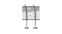
- the liquid crystal element shown in FIG. 10A has a plurality of ring-shaped transparent electrodes arranged concentrically on a transparent substrate, and applies different voltages to the individual transparent electrodes. As a result, the liquid crystal element is divided into a plurality of annular zones, and a phase difference is imparted between the light rays that have passed through different zones. Specifically, in FIG. 10A, a voltage is applied only to the transparent electrode on the right side of the drawing.
- the refractive index of the left region is the refractive index n 0 when no voltage is applied
- the refractive index of the right region is the refractive index n e because the orientation of the liquid crystal molecules is changed by voltage application. It has become. Then, a phase difference is generated between the light beam A transmitted through the left region and the light beam B transmitted through the right region due to the difference in refractive index between the regions. Further, by applying a voltage to the left transparent electrode and not applying a voltage to the right transparent electrode, it is possible to invert the phase difference generated between the light rays passing through each region.
- a step is provided on the surface of one transparent substrate on the liquid crystal layer side of the two transparent substrates sandwiching the liquid crystal layer.
- the step in the left region is higher than the step in the right region. Then, due to the difference in height of the step, a phase difference is generated between the light beam A that transmits the left region and the light beam B that transmits the right region.
- the refractive index of a resin for forming the transparent substrate and n 1 the refractive index of the liquid crystal layer to which no voltage is applied to the n 0, the refractive index of the liquid crystal layer where a voltage is applied to the case of the n e, n 1
- a voltage so as to satisfy (n 0 + n e ) / 2
- a phase difference of three values of ⁇ 1 ⁇ , 0 ⁇ , and + 1 ⁇ can be generated in the laser light.
- the three aberration amounts of ⁇ 188 m ⁇ rms, 0 m ⁇ rms, and +188 m ⁇ rms can be satisfactorily reduced.
- the liquid crystal element shown in FIG. 10B can satisfactorily reduce only three aberration amounts of -188 m ⁇ rms, 0 m ⁇ rms, and +188 m ⁇ rms. Therefore, it is not possible to satisfactorily correct aberrations caused by various variations.
- the thickness of one of the two transparent substrates sandwiching the liquid crystal layer is gradually changed.
- the thickness of the upper transparent substrate is gradually reduced from the right side toward the left side as viewed in the drawing. Then, due to the difference in thickness of the transparent substrate, a phase difference is generated between the light beam A transmitted through the left region and the light beam B transmitted through the right region.
- FIG. 10B only the three aberration amounts of ⁇ 188 m ⁇ rms, 0 m ⁇ rms, and +188 m ⁇ rms are satisfactorily reduced. Therefore, it is not possible to satisfactorily correct aberrations caused by various variations.
- the liquid crystal element 14 subtracts the phase difference that is an integral multiple of the wavelength from the phase difference that should be given to the laser light.
- the range of the phase difference to be applied is set to ⁇ 1 ⁇ or more and + 1 ⁇ or less.
- the range of the spherical aberration amount to be corrected by causing the liquid crystal element 14 to generate an aberration in the laser light transmitted through the liquid crystal element 14 is reduced.
- the range of the reduced spherical aberration amount is ⁇ S or more and + S or less
- the range of the spherical aberration amount is equally divided by an arbitrary number 2j.
- the first transparent electrode layer 146 or the fourth transparent electrode layer 149 is obtained by equally dividing the first liquid crystal layer 144 or the fourth liquid crystal layer 145 into laser light that passes through the liquid crystal element 14.
- the first liquid crystal layer 144 or the second liquid crystal layer 145 so as to generate an aberration that corrects a discrete amount of spherical aberration ( ⁇ (i / j) S, 0, + (i / j) S).
- the second transparent electrode layer 147 or the third transparent electrode layer 148 is configured such that the first liquid crystal layer 144 or the second liquid crystal layer 145 transmits ⁇ (1 / j) to the laser light transmitted through the liquid crystal element 14.
- a voltage is applied to the first liquid crystal layer 144 or the second liquid crystal layer 145 so as to generate an aberration that corrects the spherical aberration amount having a substantially continuous value within the range of S to + (1 / j) S. Apply.
- the laser beam transmitted through the liquid crystal element 14 has an aberration for correcting the discrete spherical aberration amount ( ⁇ (i / j) S, 0, + (i / j) S), and ⁇ (1 / j).
- a spherical aberration amount that occurs substantially continuously within a range from S to + (1 / j) S and below is generated by combining with correction aberration. Therefore, an aberration that substantially continuously corrects the spherical aberration amount of ⁇ S or more and + S or less can be generated in the laser light. Then, by causing the liquid crystal element 14 to generate a relatively small defocus aberration in the laser light, a large spherical aberration can be corrected.
- FIG. 11 shows a spherical aberration amount range (hereinafter, referred to as a spherical aberration amount range T) to be corrected by generating aberration in the laser beam in the liquid crystal element 14 according to the first embodiment, and the first transparent electrode layer 146.
- a spherical aberration amount (hereinafter referred to as a spherical aberration amount A) to be corrected by generating an aberration in the laser beam by driving the fourth transparent electrode layer 149, and the second transparent electrode layer 147 and the third transparent electrode layer 147.
- the relationship with the spherical aberration amount (hereinafter referred to as the spherical aberration amount B) to be corrected by generating aberration in the laser light by driving the transparent electrode layer 148 is shown.
- the spherical aberration amount range T is from ⁇ 188 m ⁇ rms to +188 m ⁇ rms.
- the spherical aberration amount range T is reduced by subtracting a phase difference that is an integral multiple of the wavelength from the phase difference that should be generated in the laser light in the liquid crystal element 14.
- the spherical aberration amount A is ⁇ 125 m ⁇ rms, 0 m ⁇ rms, and +125 m ⁇ rms.
- the spherical aberration amount B is a spherical aberration amount having a substantially continuous value in the range of ⁇ 63 m ⁇ rms to +63 m ⁇ rms.
- the first transparent electrode layer 146 and the fourth transparent electrode layer 149 are arranged such that the first liquid crystal layer 144 and the second liquid crystal layer 145 transmit ⁇ 125 m ⁇ rms, 0 m ⁇ rms, and +125 m ⁇ rms to the laser light transmitted through the liquid crystal element 14.
- a voltage is applied so as to generate an aberration that corrects the amount of spherical aberration.
- the second transparent electrode layer 147 and the third transparent electrode layer 148 are configured such that the first liquid crystal layer 144 and the second liquid crystal layer 145 transmit laser light transmitted through the liquid crystal element 14 to ⁇ 63 m ⁇ rms or more and +63 m ⁇ rms or less.
- a voltage is applied so as to generate an aberration that corrects the spherical aberration amount having a substantially continuous value in the range of. Then, by combining the aberration for correcting the spherical aberration amount A and the aberration for correcting the spherical aberration amount B (spherical aberration amount A + spherical aberration amount B), the spherical aberration within the spherical aberration amount range T is corrected substantially continuously. Aberration occurs in the laser light.
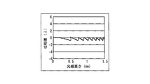
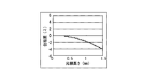
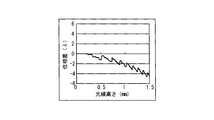
- phase difference A a phase difference imparted to the laser light transmitted through the liquid crystal element 14 is shown. 12A, B, and C to FIGS. 20A, 20B, and 20C, the second transparent electrode layer 147 or the second transparent electrode layer 147 is used to generate defocus aberration for correcting the spherical aberration amount B in the laser light transmitted through the liquid crystal element 14.
- phase difference B a phase difference imparted to the laser light transmitted through the liquid crystal element 14
- the vertical axis indicates the phase difference
- the horizontal axis indicates the ray height.
- 12A, FIG. 13A,..., FIG. 20A show the phase difference A
- FIG. 20C show the phase difference imparted to the laser light in the entire liquid crystal element 14, that is, the phase difference that combines the phase difference A and the phase difference B. Further, in the table shown in FIG. 21, in FIG.
- FIGS. 12A, B, C to FIGS. 20A, B, C the spherical aberration amount A, the spherical aberration amount B, and the total spherical surface corrected by generating defocus aberration in the laser light.
- Aberration amount spherical aberration amount A + spherical aberration amount B
- substrate thickness of recording layer coma aberration (COMA3) value, and figure number are shown in association with each other.
- the coma aberration (COMA3) is a third-order coma aberration generated by an axial deviation of 0.3 mm.
- the first transparent electrode layer 146 or the fourth transparent electrode layer 149 is the first liquid crystal layer 144 or the second liquid crystal layer 145 is the liquid crystal.
- the first liquid crystal layer 144 or the first liquid crystal layer 144 or the first liquid crystal layer 144 is provided so as to give the laser light transmitted through the element 14 a phase difference that varies substantially periodically along the radial direction of the laser light within a range of ⁇ 1 ⁇ or more and + 1 ⁇ or less.
- a voltage is applied to the second liquid crystal layer 145.
- a laser beam is emitted from the liquid crystal element 14. Shows the amount of phase difference generated.
- FIG. 12A when the first transparent electrode layer 146 or the fourth transparent electrode layer 149 is driven, the liquid crystal element 14 emits laser light within the range of ⁇ 1 ⁇ to 0 ⁇ .
- a phase difference that changes substantially periodically along the radial direction of the is provided.
- the first liquid crystal layer 144 or the fourth liquid crystal layer 149 is applied with a voltage from the first transparent electrode layer 146 or the fourth transparent electrode layer 149, whereby the first transparent electrode layer 146 or the fourth liquid crystal layer 149 is applied.
- the fourth transparent electrode layer 149 has a portion that imparts a phase difference of ⁇ 1 ⁇ between laser beams that pass through adjacent transparent electrodes.
- an aberration for correcting spherical aberration of ⁇ 125 m ⁇ rms spherical aberration amount A
- the second transparent electrode layer 147 or the third transparent electrode layer 148 is driven, so that the liquid crystal element 14 causes the laser light to travel approximately along the radial direction of the laser light.
- a phase difference that changes substantially continuously from ⁇ 4 ⁇ to 0 ⁇ is given.
- the liquid crystal element 14 is driven by driving the first transparent electrode layer 146 and the second transparent electrode layer 147 or the third transparent electrode layer 148 and the fourth transparent electrode layer 149.
- the phase difference A and the phase difference B are imparted to the laser light.
- the liquid crystal element 14 can generate an aberration for correcting the spherical aberration amount A and the spherical aberration amount B in the laser light.
- COMP3 coma aberration
- the first liquid crystal layer 144 or the fourth liquid crystal layer 149 is applied with a voltage from the first transparent electrode layer 146 or the fourth transparent electrode layer 149, whereby the first transparent electrode layer 146 or the fourth liquid crystal layer 149 is applied.
- the fourth transparent electrode layer 149 has a portion that imparts a phase difference of ⁇ 1 ⁇ between laser beams that pass through adjacent transparent electrodes. As a result, an aberration for correcting spherical aberration of ⁇ 125 m ⁇ rms (spherical aberration amount A) can be generated in the laser light.
- the phase difference imparted to the laser light in the entire liquid crystal element 14 is only the phase difference A.
- the liquid crystal element 14 By driving the first transparent electrode layer 146 or the fourth transparent electrode layer 149, the liquid crystal element 14 imparts a phase difference A to the laser light. Thereby, the liquid crystal element 14 can generate an aberration for correcting the spherical aberration amount A in the laser light. Further, it is possible to reduce spherical aberration that occurs when light is condensed on a recording layer having a substrate thickness of 0.100 mm and coma aberration (COMA3) of 0.1 m ⁇ rms.
- COMP3 coma aberration
- the first liquid crystal layer 144 or the fourth liquid crystal layer 149 is applied with a voltage from the first transparent electrode layer 146 or the fourth transparent electrode layer 149, whereby the first transparent electrode layer 146 or the fourth liquid crystal layer 149 is applied.
- the fourth transparent electrode layer 149 has a portion that imparts a phase difference of ⁇ 1 ⁇ between laser beams that pass through adjacent transparent electrodes.
- an aberration for correcting spherical aberration of ⁇ 125 m ⁇ rms spherical aberration amount A
- the liquid crystal element 14 causes the laser light to emit 0 ⁇ along the radial direction of the laser light.
- the liquid crystal element 14 is driven by driving the first transparent electrode layer 146 and the second transparent electrode layer 147 or the third transparent electrode layer 148 and the fourth transparent electrode layer 149.
- the phase difference A and the phase difference B are imparted to the laser light.
- the liquid crystal element 14 can generate an aberration for correcting the spherical aberration amount A and the spherical aberration amount B in the laser light.
- COMP3 coma aberration
- the liquid crystal element 14 uses laser light. Shows the amount of phase difference generated.
- the second transparent electrode layer 147 or the third transparent electrode layer 148 is driven, so that the liquid crystal element 14 causes the laser light to travel approximately along the radial direction of the laser light.
- a phase difference that changes substantially continuously from ⁇ 4 ⁇ to 0 ⁇ is given.
- the liquid crystal element 14 can generate an aberration for correcting the spherical aberration amount B in the laser light. Further, it is possible to reduce spherical aberration that occurs when light is condensed on a recording layer having a substrate thickness of 0.093 mm and coma aberration (COMA3) of 1.6 m ⁇ rms.
- spherical aberration amount B substantially continuous spherical aberration
- FIGS. 16A to 16C in order to reduce the spherical aberration generated when the light is condensed on the recording layer having a substrate thickness of 0.088 mm and the coma aberration (COMA3) of 0.0 m ⁇ rms, laser light is emitted from the liquid crystal element 14. Shows the amount of phase difference generated.
- the phase difference imparted to the laser light in the entire liquid crystal element 14 is also zero.
- the liquid crystal element 14 uses laser light. Shows the amount of phase difference generated.
- the liquid crystal element 14 receives 0 ⁇ along the radial direction of the laser light. To approximately + 4 ⁇ is given a phase difference that changes substantially continuously.
- the liquid crystal element 14 can generate an aberration for correcting the spherical aberration amount B in the laser light. Further, it is possible to reduce spherical aberration that occurs when light is condensed on a recording layer having a substrate thickness of 0.082 mm and coma aberration (COMA3) of 2.5 m ⁇ rms.
- spherical aberration amount B substantially continuous spherical aberration
- the first liquid crystal layer 144 or the fourth liquid crystal layer 149 is applied with a voltage from the first transparent electrode layer 146 or the fourth transparent electrode layer 149, whereby the first transparent electrode layer 146 or the fourth liquid crystal layer 149 is applied.
- 4 has a portion that gives a phase difference of + 1 ⁇ between laser beams that pass through adjacent transparent electrodes of the transparent electrode layer 149.
- an aberration for correcting the spherical aberration of +125 m ⁇ rms spherical aberration amount A
- the liquid crystal element 14 causes the laser light to travel approximately along the radial direction of the laser light.
- a phase difference that changes substantially continuously from ⁇ 4 ⁇ to 0 ⁇ is given.
- the liquid crystal element 14 is driven by driving the first transparent electrode layer 146 and the second transparent electrode layer 147 or the third transparent electrode layer 148 and the fourth transparent electrode layer 149.
- the phase difference A and the phase difference B are imparted to the laser light.
- the liquid crystal element 14 can generate an aberration for correcting the spherical aberration amount A and the spherical aberration amount B in the laser light.
- COMP3 coma aberration
- the first liquid crystal layer 144 or the fourth liquid crystal layer 149 is applied with a voltage from the first transparent electrode layer 146 or the fourth transparent electrode layer 149, whereby the first transparent electrode layer 146 or the fourth liquid crystal layer 149 is applied.
- 4 has a portion that gives a phase difference of + 1 ⁇ between laser beams that pass through adjacent transparent electrodes of the transparent electrode layer 149.
- an aberration for correcting the spherical aberration of +125 m ⁇ rms spherical aberration amount A
- spherical aberration amount A can be generated in the laser light.
- spherical aberration that occurs when the light is condensed on the recording layer having a substrate thickness of 0.076 mm can be reduced.
- the liquid crystal element 14 By driving the first transparent electrode layer 146 or the fourth transparent electrode layer 149, the liquid crystal element 14 imparts a phase difference A to the laser light. Thereby, the liquid crystal element 14 can generate an aberration for correcting the spherical aberration amount A in the laser light. Further, it is possible to reduce spherical aberration that occurs when light is condensed on a recording layer having a substrate thickness of 0.076 mm and coma aberration (COMA3) of 3.4 m ⁇ rms.
- COMP3 coma aberration
- the first transparent electrode layer 146 or the fourth transparent electrode layer 149 is driven, so that the liquid crystal element 14 emits laser light within the range of 0 ⁇ or more and + 1 ⁇ or less.
- a phase difference that changes substantially periodically along the radial direction is applied.
- the first liquid crystal layer 144 or the fourth liquid crystal layer 149 is applied with a voltage from the first transparent electrode layer 146 or the fourth transparent electrode layer 149, whereby the first transparent electrode layer 146 or the fourth liquid crystal layer 149 is applied.
- 4 has a portion that gives a phase difference of + 1 ⁇ between laser beams that pass through adjacent transparent electrodes of the transparent electrode layer 149.
- an aberration for correcting the spherical aberration of +125 m ⁇ rms spherical aberration amount A
- the second transparent electrode layer 147 or the third transparent electrode layer 148 is driven to cause the liquid crystal element 14 to emit 0 ⁇ along the radial direction of the laser light.
- the liquid crystal element 14 is driven by driving the first transparent electrode layer 146 and the second transparent electrode layer 147 or the third transparent electrode layer 148 and the fourth transparent electrode layer 149.
- the phase difference A and the phase difference B are imparted to the laser light.
- the liquid crystal element 14 can generate an aberration for correcting the spherical aberration amount A and the spherical aberration amount B in the laser light.
- COMP3 coma aberration
- the spherical aberration amount (spherical aberration amount A + spherical aberration amount B) corrected by the element 14 by causing aberration in the laser light is the same.
- the spherical aberration amount corrected by causing the liquid crystal element 14 to generate aberration in the laser light in FIGS. 17A to 17C and the spherical aberration amount corrected by causing the liquid crystal element 14 to generate aberration in the laser light in FIGS. 18A to 18C. Is the same.
- the phase difference B is a defocus component that is proportional to the square of the ray height (r). Accordingly, the phase difference imparted to the laser light by the liquid crystal element 14 includes a defocus component.
- the objective lens 17 is operated by the actuator, so that an axial deviation occurs between the liquid crystal element 14 and the objective lens 17.
- the liquid crystal element 14 causes the laser beam transmitted through the liquid crystal element 14 to be proportional to the fourth power of the light beam height (r).
- Spherical aberration is generated.
- a large coma aberration proportional to the cube of the ray height (r) is generated.
- the aberration generated in the laser light is as follows. Only the tilt component proportional to the first power of the ray height (r) remains.
- the tilt component does not affect the spot shape of the laser light. For this reason, the coma aberration due to axial misalignment or the like can be reduced by including a defocus component in the phase difference that the liquid crystal element 14 gives to the laser light transmitted through the liquid crystal element 14.
- a phase difference A that changes substantially periodically along the radial direction of the laser beam within a range of ⁇ 1 ⁇ or more and 0 ⁇ or less is given to the laser beam.
- an aberration for correcting the spherical aberration amount A of ⁇ 125 m ⁇ rms is generated.
- a phase difference B that changes substantially continuously from about ⁇ 4 ⁇ to about + 4 ⁇ along the radial direction of the laser light is given to the laser light.
- an aberration for correcting the spherical aberration amount B having a substantially continuous value from ⁇ 63 m ⁇ rms to +63 m ⁇ rms is generated.
- the liquid crystal element 14 generates a spherical aberration amount from ⁇ 188 m ⁇ rms to ⁇ 63 m ⁇ rms substantially continuously by generating a laser beam with an aberration that corrects the spherical aberration amount A and an aberration that corrects the spherical aberration amount B.
- Aberrations to be corrected are generated.
- the maximum absolute value of the sum of the phase difference A and the phase difference B is about 4 ⁇ .
- a phase difference A that substantially changes periodically along the radial direction of the laser beam within a range of 0 ⁇ or more and + 1 ⁇ or less is given to the laser beam.
- an aberration for correcting the spherical aberration amount A of +125 m ⁇ rms is generated.
- the laser beam is given a phase difference B that changes substantially continuously from about ⁇ 4 ⁇ to about + 4 ⁇ along the radial direction of the laser beam.
- an aberration for correcting the spherical aberration amount B having a substantially continuous value from ⁇ 63 m ⁇ rms to +63 m ⁇ rms is generated.
- the liquid crystal element 14 generates a spherical aberration amount from +63 m ⁇ rms to +188 m ⁇ rms substantially continuously by generating, in the laser beam, an aberration that corrects the spherical aberration amount A and an aberration that corrects the spherical aberration amount B.
- An aberration to be corrected is generated.
- the maximum absolute value of the sum of the phase difference A and the phase difference B is about 4 ⁇ .
- the liquid crystal element 14 generates a spherical aberration amount from ⁇ 63 m ⁇ rms to +63 m ⁇ rms substantially continuously by generating, in the laser beam, an aberration that corrects the spherical aberration amount A and an aberration that corrects the spherical aberration amount B. Aberrations to be corrected are generated.
- the maximum absolute value of the sum of the phase difference A and the phase difference B is about 4 ⁇ .
- the liquid crystal element 14 according to the example 1 causes the laser light to substantially continuously correct the aberration for correcting the spherical aberration of ⁇ 188 m ⁇ rms to +188 m ⁇ rms. Can be generated. Further, the maximum value of the absolute value of the phase difference imparted to the laser light by the liquid crystal element 14 in order to generate an aberration for correcting the spherical aberration substantially continuously in the laser light is about 4 ⁇ . On the other hand, the absolute value of the phase difference imparted to the laser light is about 13 ⁇ as shown in FIG.
- the liquid crystal element 14 in order to cause the conventional liquid crystal element to generate an aberration that substantially continuously corrects the spherical aberration in the laser light. is there. Therefore, by using the liquid crystal element 14 according to the first embodiment, it is possible to reduce the phase difference to be imparted to the laser light to correct the spherical aberration to about 1/3. In other words, the liquid crystal element 14 can correct large aberrations substantially continuously by giving a relatively small phase difference to the laser light.
- the phase difference imparted to the laser light transmitted through the liquid crystal element 14 is as shown in FIGS. 12A, B, C to 20A, It is not a continuous value as shown in B and C, but a value that changes stepwise.
- 22A to 22C show the phase difference actually applied to the laser light by the liquid crystal element 14.
- FIG. 22A to 22C show the case where a phase difference having the same value as the phase difference shown in FIGS. 12A to 12C is given to the laser light.
- 22A shows the phase difference A
- FIG. 22B shows the phase difference B.
- FIG. 22C shows the phase difference imparted to the laser light in the entire liquid crystal element 14, that is, the phase difference that combines the phase difference A and the phase difference B.
- each transparent electrode has a phase difference that is different by 0.2 ⁇ for each ring zone of each transparent electrode.
- the electrode applies a voltage.
- the phase difference given to the laser light increases by -0.2 ⁇ .
- the phase difference imparted to the laser beam reaches ⁇ 1 ⁇ in the fifth ring zone from the optical axis, the phase difference imparted to the laser beam transmitted through the sixth ring zone becomes 0 ⁇ .
- the phase difference between the laser beam that has passed through the fifth ring zone and the laser beam that has passed through the sixth zone is 1 ⁇ .
- the phase difference imparted to the laser light increases by ⁇ 0.2 ⁇ from the 6th ring zone to the 10th ring zone.
- a phase difference that changes substantially periodically along the radial direction of the is provided.
- the first liquid crystal layer 144 and the second liquid crystal layer 145 have the first transparent electrode layer 146 and the second transparent electrode layer 145.
- the fourth transparent electrode layer 149 has a portion that gives a phase difference of 1 ⁇ between laser beams that pass through adjacent transparent electrodes. Specifically, as shown in FIG. 22A, the phase difference between the laser light that passes through the five annular zones and the laser light that passes through the six annular zones, the laser light that passes through the ten annular zones, and the laser that passes through the eleven annular zones.
- the phase difference between the laser light and the laser light transmitted through the 36 annular zone, and the phase difference between the laser light transmitted through the 40 annular zone and the laser light transmitted through the 41 annular zone are 1 ⁇ .
- an electric field is generated at a boundary portion between adjacent transparent electrodes due to a potential difference between the adjacent transparent electrodes, or the direction of liquid crystal molecules changes smoothly. Therefore, the phase of the laser beam that passes through the boundary portion between adjacent transparent electrodes changes smoothly.
- the number of ring zones of the transparent electrode provided in the 1st transparent electrode layer 146 and the 4th transparent electrode layer 149 is 43 ring zones.
- the number of ring zones of the transparent electrodes provided in the second transparent electrode layer 147 and the third transparent electrode layer 148 is 20. Therefore, the transparent electrode provided in the second transparent electrode layer 147 and the third transparent electrode layer 148 is equal to the number of ring zones of the transparent electrode provided in the first transparent electrode layer 146 and the fourth transparent electrode layer 149. It is more than the number of ring zones. As shown in FIG.
- the number of extraction electrodes can be reduced by connecting the annular zones to which the same voltage is applied to form one transparent electrode.
- FIG. 22B in the second transparent electrode layer 147 and the third transparent electrode layer 148, there is no ring zone to which the same voltage is applied. Therefore, it is necessary to provide a lead electrode on the transparent electrode of each ring zone. Therefore, if the number of ring zones of the transparent electrode in the second transparent electrode layer 147 and the third transparent electrode layer 148 is large, the area occupied by the extraction electrode is increased accordingly.
- the number of ring zones of the transparent electrode formed on the liquid crystal element 14 is small.
- the number of transparent electrode zones formed on the liquid crystal element 14 increases, aberration correction can be performed more continuously, so that the light utilization efficiency is improved. Therefore, the number of zones of the transparent electrodes formed on the first transparent electrode layer 146 and the fourth transparent electrode layer 149 that can reduce the number of extraction electrodes is set to the second transparent electrode layer 147 and the third transparent electrode layer. It is preferable to increase the number of ring zones of the transparent electrode formed in 148. As a result, the area occupied by the extraction electrode in the liquid crystal element 14 can be reduced while improving the light utilization efficiency.
- a large aberration is corrected by giving a relatively small phase difference to the laser beam by the liquid crystal element 14, and the correction aberration is not limited to the spherical aberration.
- the phase difference generated in the liquid crystal element 14 is a defocus component proportional to the square of the light beam height.
- the defocus component may be reduced to include a spherical aberration component. Good.
- Optical pickup optical system 11
- Laser diode (laser light source) 14
- Liquid crystal element 141
- First transparent substrate (first transparent substrate) 142
- Second transparent substrate (second transparent substrate) 143
- Third transparent substrate (first transparent substrate) 144
- First liquid crystal layer (refractive index anisotropic medium layer) 145
- Second liquid crystal layer (refractive index anisotropic medium layer) 146
- First transparent electrode layer (first transparent electrode layer) 147
- Second transparent electrode layer (second transparent electrode layer) 148
- Third transparent electrode layer (second transparent electrode layer) 149
- Fourth transparent electrode layer (first transparent electrode layer) 17
- Objective lens 19
Landscapes
- Physics & Mathematics (AREA)
- Optics & Photonics (AREA)
- Nonlinear Science (AREA)
- Chemical & Material Sciences (AREA)
- Crystallography & Structural Chemistry (AREA)
- General Physics & Mathematics (AREA)
- Optical Head (AREA)
- Liquid Crystal (AREA)
Abstract
第1の液晶層144を駆動する第1の透明電極層146及び第2の透明電極層147を備える液晶素子14であって、第1の透明電極層146は、第1の液晶層144が、液晶素子14を透過するレーザ光に、-hλ以上、+hλ以下の範囲内(hは、h≧1を満たす整数、λは設計波長)で、レーザ光の径方向に沿って略周期的に変化する位相差を付与するとともに、第1の透明電極層146の隣り合う透明電極を透過するレーザ光間にhλの位相差を付与する部分を有するように、第1の液晶層144に電圧を印加し、第2の透明電極層147は、第1の液晶層144が、液晶素子14を透過するレーザ光に、レーザ光の径方向に沿って略連続的に変化する位相差を付与するように、第1の液晶層144に電圧を印加するように構成した。
Description
本発明は、液晶素子及び光ピックアップ光学系に関する。
最近、大画面薄型ディスプレイの普及により、高精細度で映像などを記録するニーズが高まっている。これに伴い、BD(Blu-ray Disc)などの光ディスクの記録容量の増大も図られている。例えば、記録層の多層化が試みられ、既に、50GBの2層BDも商品化されている。
多層光記録媒体を光ピックアップ光学系で記録再生する場合、多層光記録媒体の表面から各記録層までの厚み(基板厚み)の違いによって球面収差が発生する。球面収差は開口数(NA:Numerical Aperture)の4乗に比例する。また、BDのNAは0.85であり、DVD(Digital Versatile Disc)のNAは0.65である。そのため、DVDなどの従来の光ディスクに比べて、BDを記録再生する際に発生する球面収差は増大しやすい。したがって、BDを記録再生する光ピックアップ光学系では、各記録層の基板厚みの違いに基づく球面収差を低減する補正機構が必須である。
多層光記録媒体を光ピックアップ光学系で記録再生する場合、多層光記録媒体の表面から各記録層までの厚み(基板厚み)の違いによって球面収差が発生する。球面収差は開口数(NA:Numerical Aperture)の4乗に比例する。また、BDのNAは0.85であり、DVD(Digital Versatile Disc)のNAは0.65である。そのため、DVDなどの従来の光ディスクに比べて、BDを記録再生する際に発生する球面収差は増大しやすい。したがって、BDを記録再生する光ピックアップ光学系では、各記録層の基板厚みの違いに基づく球面収差を低減する補正機構が必須である。
また、BD用の対物レンズの材質として、ガラス、プラスティックなどが検討されている。プラスティックの生産性は、ガラスよりも優れる。しかし、プラスティックの温度変化に伴う屈折率変化は、ガラスよりも大きい。そのため、プラスティックにより形成された対物レンズにおいて発生する球面収差は、温度変化によっても増大しやすい。したがって、温度変化によって発生する球面収差を低減する補正機構の開発も望まれている。
球面収差の補正技術としては、対物レンズの結像倍率を変化させるものがある。対物レンズの結像倍率を変化させることにより、基板厚みの違いに基づく球面収差と反対の符号を持つ球面収差を発生させ、球面収差の低減を図っている。特許文献1には、対物レンズの結像倍率を変化させるため、光源と対物レンズとの間に配置されたコリメータレンズの位置を可動させる技術が記載されている。これにより、DVDとCD(Compact Disc)との互換を行っている。
また、特許文献2には、光ピックアップ光学系における各レンズを可動させ、各レンズ間の間隔を変化させる技術が記載されている。これにより、2層光記録媒体における各記録層の基板厚みの違いに基づく球面収差を低減している。
また、特許文献2には、光ピックアップ光学系における各レンズを可動させ、各レンズ間の間隔を変化させる技術が記載されている。これにより、2層光記録媒体における各記録層の基板厚みの違いに基づく球面収差を低減している。
また、他の球面収差の補正技術としては、補正機能を持った液晶素子を用いるものがある。例えば、特許文献3には、対物レンズと液晶素子をアクチュエータに搭載し、対物レンズと液晶素子とを一体的に可動する技術が記載されている。これにより、トラッキングに伴う軸ズレによる収差劣化を防止している。また、液晶素子駆動信号とアクチュエータ駆動信号とを重畳することにより、アクチュエータに接続する弾性支持体の数を減らす技術も記載されている。
また、特許文献4には、液晶素子を駆動する半導体素子をアクチュエータに搭載し、当該半導体素子を駆動する駆動信号のみをアクチュエータの弾性支持体を介して導通する技術が記載されている。これにより、弾性支持体の数をさらに低減している。
また、特許文献5には、各記録層の基板厚みの違いに基づく球面収差を補正する液晶素子と、各光記録媒体の記録層の基板厚みのばらつきなどに基づく球面収差を補正する液晶素子とを備える光ピックアップ光学系が記載されている。
また、特許文献6には、2枚の透明基板と、当該2枚の透明基板間に挟持された液晶層と、からなる液晶素子を備える光ピックアップ光学系が記載されている。特許文献6では、一方の透明基板の液晶層側にブレーズ格子を設けている。また、2枚の透明基板のそれぞれに、輪帯状に形成された大きさの異なる複数の透明電極が光軸を同心として同心円状に配置された透明電極層を設けている。そして、グレーズ格子が設けられた透明基板の透明電極層に電圧を印加することにより、各記録層の基板厚みの違いに基づく球面収差を補正し、もう一方の透明基板の透明電極層に電圧を印加することにより、各光記録媒体の記録層の基板厚みのばらつきなどに基づく球面収差を補正している。
また、特許文献7には、2枚の透明基板に挟持された液晶層を有する液晶素子が記載されている。そして、一方の透明基板に、各記録層の基板厚みの違いに基づく球面収差を補正する第1の透明電極層を設け、他方の透明基板に、各光記録媒体の記録層の基板厚みのばらつきなどに基づく球面収差を補正する第2の透明電極層を設けている。第1の透明電極層及び第2の透明電極層は、輪帯状に形成された大きさの異なる複数の透明電極が光軸を同心として同心円状に配置されてなる。また、位相差が波長の整数倍であることは位相差がないのと同じであることを利用して、第1の透明電極層に電圧を印加して発生させる位相差を低減している。具体的には、第1の透明電極層に電圧を印加することにより、各記録層の基板厚みの違いに基づく球面収差を補正するために必要な位相差から波長の整数倍の位相差を差し引いた位相差を発生させている。これにより、液晶層の厚みの低減を図っている。
しかしながら、特許文献1及び2では、レンズを駆動する機構が必要となるため、光ピックアップ光学系が大型になってしまうという問題がある。
また、特許文献3及び4では、アクチュエータに液晶素子を搭載するため、アクチュエータが大型になってしまうという問題がある。また、アクチュエータの重量が増加するため、アクチュエータの周波数応答性能が劣化する。そのため、高速な信号再生の障害となるという問題がある。
また、特許文献5では、液晶素子が2つ必要となるため、部品点数の増加、装置の大型化、高コスト化を招くという問題がある。
また、特許文献3及び4では、アクチュエータに液晶素子を搭載するため、アクチュエータが大型になってしまうという問題がある。また、アクチュエータの重量が増加するため、アクチュエータの周波数応答性能が劣化する。そのため、高速な信号再生の障害となるという問題がある。
また、特許文献5では、液晶素子が2つ必要となるため、部品点数の増加、装置の大型化、高コスト化を招くという問題がある。
また、特許文献6では、半径方向において、一方の透明基板に設けられる透明電極の位置と、他方の透明基板に設けられる透明電極の位置とを合わせる必要がある。そのため、収差補正の自由度が低下するという問題がある。例えば、2層BDのそれぞれの記録層の基板厚みが0.075mm、0.1mmである場合、各記録層の基板厚みの違いに基づく球面収差を補正するための位相差を付与する透明電極層の各透明電極の輪帯幅が広くなる。そのため、各光記録媒体の記録層の基板厚みのばらつきなどに基づく球面収差を補正するための位相差を付与する透明電極層の各透明電極の輪帯幅も広くなり、連続的な位相成分を発生させることができなくなる。結果として、例えば、補正可能な基板厚みのばらつきの範囲は、0.075±0.005mm、0.1±0.005mm程度となってしまう可能性がある。この場合、レーザ光源の出射光束の波長のばらつき、対物レンズのばらつき、温度変化による球面収差の変化などに基づく様々な収差を補正することはできない。
また、特許文献7では、各記録層の基板厚みの違いに基づく球面収差を補正する第1の透明電極層の透明電極数が多く、各透明電極に異なる電圧を付与する必要がある。そのため、各透明電極からの引き出し電極が多くなり、液晶素子表面における引き出し電極の配線部分が占める割合が大きくなる。そのため、引き出し電極の配線部分において大きな収差が発生してしまうという問題がある。
本発明は、このような問題点を解決するためになされたものであり、大きな収差を略連続的に補正可能な液晶素子及び光ピックアップ光学系を提供することを目的とする。
本発明にかかる液晶素子は、第1の透明基板と、前記第1の透明基板と対向する第2の透明基板と、前記第1の透明基板と前記第2の透明基板との間に挟持される屈折率異方性媒質層とを備えている。また、当該液晶素子は、前記第1の透明基板に、略輪帯状に形成された大きさの異なる複数の第1の透明電極が光軸を中心として同心円状に配設されてなる第1の透明電極層と、前記第2の透明基板に、略輪帯状に形成された大きさの異なる複数の第2の透明電極が光軸を中心として同心円状に配設されてなる第2の透明電極層と、を備えている。また、前記第1の透明電極層において、略同じ値の電圧を印加する前記第1の透明電極が前記第1の透明基板の径方向に略周期的に配設されている。また、前記第1の透明電極層は、前記屈折率異方性媒質層が、前記液晶素子を透過する光束に、-hλ以上、+hλ以下の範囲内(hは、h≧1を満たす整数、λは設計波長)で、光束の径方向に沿って略周期的に変化する位相差を付与するとともに、隣り合う前記第1の透明電極を透過する光束間にhλの位相差を付与する部分を有するように、前記屈折率異方性媒質層に電圧を印加する。また、前記第2の透明電極層は、前記屈折率異方性媒質層が、前記液晶素子を透過する光束に、光束の径方向に沿って略連続的に変化する位相差を付与するように、前記屈折率異方性媒質層に電圧を印加するものである。
本発明においては、第1の透明電極層において、略同じ値の電圧を印加する第1の透明電極が第1の透明基板の径方向に略周期的に配設されている。また、第1の透明電極層によって電圧が印加されることにより、屈折率異方性媒質層が、液晶素子を透過する光束に、-hλ以上、+hλ以下の範囲内で、光束の径方向に沿って略周期的に変化する位相差を付与する。これにより、液晶素子は、液晶素子を透過する光束に、-1λ以下、+1λ以上の大きな位相差を付与することができる。具体的には、位相差が波長の整数倍であることは位相差がないのと同じであるため、-1λ以下、+1λ以上の大きな位相差は、当該位相差から波長の整数倍の位相差を差し引いたものと等価である。-1λ以下、+1λ以上の大きな位相差から波長の整数倍の位相差を差し引くと、-1λ以上、+1λ以下の範囲内で、光束の径方向に沿って略周期的に変化する位相差となる。そのため、屈折率異方性媒質層が、液晶素子を透過する光束に、-1λ以上、+1λ以下の範囲内(この場合、h=1)で、光束の径方向に沿って略周期的に変化する位相差を付与することにより、当該光束に、-1λ以下、+1λ以上の大きな位相差を付与することができる。
また、第1の透明電極層によって電圧が印加されることにより、屈折率異方性媒質層は、隣り合う第1の透明電極を透過する光束間にhλの位相差を付与する部分を有する。そして、第1の透明電極層によって電圧が印加された屈折率異方性媒質層は、このような位相差を光束に付与することにより、光束に、デフォーカス収差を発生させることができる。そして、当該デフォーカス収差により、球面収差を補正することができる。また、当該デフォーカス収差は、-1λ以下、+1λ以上の大きな位相差に基づくものである。そのため、当該デフォーカス収差量は大きな値となる。したがって、第1の透明電極層によって屈折率異方性媒質層に電圧を印加することにより、液晶素子を透過する光束に、-hλ以上、+hλ以下の範囲内の比較的制限された位相差を付与するだけで、-1λ以下、+1λ以上の大きな位相差に基づく大きなデフォーカス収差を発生させることができ、大きな球面収差を補正することができる。
また、第1の透明電極層によって電圧が印加されることにより、屈折率異方性媒質層は、隣り合う第1の透明電極を透過する光束間にhλの位相差を付与する部分を有する。そして、第1の透明電極層によって電圧が印加された屈折率異方性媒質層は、このような位相差を光束に付与することにより、光束に、デフォーカス収差を発生させることができる。そして、当該デフォーカス収差により、球面収差を補正することができる。また、当該デフォーカス収差は、-1λ以下、+1λ以上の大きな位相差に基づくものである。そのため、当該デフォーカス収差量は大きな値となる。したがって、第1の透明電極層によって屈折率異方性媒質層に電圧を印加することにより、液晶素子を透過する光束に、-hλ以上、+hλ以下の範囲内の比較的制限された位相差を付与するだけで、-1λ以下、+1λ以上の大きな位相差に基づく大きなデフォーカス収差を発生させることができ、大きな球面収差を補正することができる。
しかし、第1の透明電極層によって屈折率異方性媒質層に電圧を印加することにより、液晶素子を透過する光束に発生されるデフォーカス収差は、離散的な値となってしまう。そこで、本発明においては、第2の透明電極層によって電圧が印加されることにより、屈折率異方性媒質層が、液晶素子を透過する光束に、光束の径方向に沿って略連続的に変化する位相差を付与する。これにより、液晶素子を透過する光束に所定の範囲内で略連続的な値の収差を発生させることができる。そして、第1の透明電極層によって電圧が印加されることにより、屈折率異方性媒質層が、液晶素子を透過する光束に付与する離散的なデフォーカス収差と、当該略連続的な値のデフォーカス収差とが合わさる。したがって、第1の透明電極層及び第2の透明電極層によって電圧が印加されることにより、屈折率異方性媒質層が、液晶素子を透過する光束に-1λ以下、+1λ以上の大きな位相差に基づく大きなデフォーカス収差であって略連続的なデフォーカス収差を発生させることができる。これにより、当該液晶素子は、大きな収差を略連続的に補正することができる。
また、前記液晶素子により、当該液晶素子を透過する光束に収差を発生させることにより補正する球面収差量の範囲が-S以上、+S以下(Sは正の数)である場合に、前記第1の透明電極層は、前記屈折率異方性媒質層が、前記液晶素子を透過する光束に、-(i/j)S(jが奇数の場合、iは、i≦jを満たす偶数、jが偶数の場合、iは、i≦jを満たす奇数)、0、+(i/j)Sの球面収差量を補正するような収差を発生させるように、前記屈折率異方性媒質層に電圧を印加することが好ましい。
さらに、前記第2の透明電極層は、前記屈折率異方性媒質層が、前記液晶素子を透過する光束に、-(1/j)S以上、+(1/j)S以下の範囲内で略連続的な値の球面収差量を補正するような収差を発生させるように、前記屈折率異方性媒質層に電圧を印加することが好ましい。
さらに、前記第2の透明電極層は、前記屈折率異方性媒質層が、前記液晶素子を透過する光束に、-(1/j)S以上、+(1/j)S以下の範囲内で略連続的な値の球面収差量を補正するような収差を発生させるように、前記屈折率異方性媒質層に電圧を印加することが好ましい。
これにより、液晶素子を透過する光束に発生させた収差により補正する球面収差量の範囲を任意の数2jで等分し、第1の透明電極層を駆動することにより、屈折率異方性媒質層は、等分して得られる離散的な値の球面収差量(-(i/j)S、0、+(i/j)S)を補正するようなデフォーカス収差を当該光束に発生させる。このとき、第2の透明電極層を駆動することにより、-(1/j)S以上、+(1/j)S以下の範囲内で略連続的な値の球面収差を補正するような収差を当該光束に発生させると、当該光束に、-S以上、+S以下の球面収差量を略連続的に補正するような収差を発生させることができる。そして、jの数を大きくする程、第2の透明電極層を駆動することにより、当該光束に発生させる収差の範囲を小さくすることができる。したがって、jの数を大きくすることにより、第2の透明電極層の第2の透明電極の輪帯数を少なくすることができる。
また、前記液晶素子は、レーザ光源からの光束を光記録媒体に集光する光ピックアップ光学系の所定位置に固定して配置されており、前記液晶素子が前記液晶素子を透過する光束に与える位相差は、デフォーカス成分を含むことが好ましい。
通常、液晶素子を光ピックアップ光学系の所定位置に固定して配置すると、アクチュエータによって対物レンズが動作することにより、液晶素子と対物レンズとの間に軸ズレが生じる。また、光記録媒体の各記録層の基板厚みの違いに基づく球面収差を補正するために、液晶素子により、液晶素子を透過する光束に、光線高さの4乗に比例する球面収差を発生させる。このとき、軸ズレなどが発生すると、光線高さの3乗に比例する大きなコマ収差が発生する。このとき、液晶素子により、液晶素子を透過する光束に、光線高さの2乗に比例するデフォーカス成分を含む位相差を付与すると、当該光束に発生する収差としては、光線高さの1乗に比例するチルト成分のみが残る。当該チルト成分は、光束のスポット形状に影響を与えない。そのため、液晶素子が当該液晶素子を透過する光束に与える位相差に、デフォーカス成分を含むことにより、軸ズレなどに起因するコマ収差を低減することができる。
通常、液晶素子を光ピックアップ光学系の所定位置に固定して配置すると、アクチュエータによって対物レンズが動作することにより、液晶素子と対物レンズとの間に軸ズレが生じる。また、光記録媒体の各記録層の基板厚みの違いに基づく球面収差を補正するために、液晶素子により、液晶素子を透過する光束に、光線高さの4乗に比例する球面収差を発生させる。このとき、軸ズレなどが発生すると、光線高さの3乗に比例する大きなコマ収差が発生する。このとき、液晶素子により、液晶素子を透過する光束に、光線高さの2乗に比例するデフォーカス成分を含む位相差を付与すると、当該光束に発生する収差としては、光線高さの1乗に比例するチルト成分のみが残る。当該チルト成分は、光束のスポット形状に影響を与えない。そのため、液晶素子が当該液晶素子を透過する光束に与える位相差に、デフォーカス成分を含むことにより、軸ズレなどに起因するコマ収差を低減することができる。
また、液晶素子を光ピックアップ光学系の所定位置に固定して配置することにより、液晶素子を対物レンズとともにアクチュエータに搭載する場合に比べて、アクチュエータの重量を低減することができる。これにより、アクチュエータの周波数応答性を劣化させずに済む。そのため、高速な信号再生を実現することができる。
さらに、また、前記第1の透明電極層は、異なる電圧が印加される複数本の前記第1の透明電極を有し、前記第1の透明電極は、同じ電圧が印加される複数の輪帯状の透明電極を備え、前記輪帯状の透明電極は、一部が欠失されてなる端部を有し、前記内側の輪帯状の透明電極の端部と、前記内側の輪帯状の透明電極と同じ電圧を印加する外側の輪帯状の透明電極の端部と、が略半径方向に沿って引き出し電極により順次接続され、複数本の前記第1の透明電極の前記引き出し電極が互いに重なり合わないように配置されていることが好ましい。
これにより、同じ電圧を印加する複数の輪帯状の電極を1本の第1の透明電極とすることができる。そして、引き出し電極の本数を第1の透明電極に印加する電圧数とすることができる。よって、引き出し電極の領域を最小限に抑えることができ、液晶素子の収差補正性能の低下を防ぐことができる。
これにより、同じ電圧を印加する複数の輪帯状の電極を1本の第1の透明電極とすることができる。そして、引き出し電極の本数を第1の透明電極に印加する電圧数とすることができる。よって、引き出し電極の領域を最小限に抑えることができ、液晶素子の収差補正性能の低下を防ぐことができる。
また、前記第1の透明電極層に設けられる前記第1の透明電極の輪帯数よりも、前記第2の透明電極層に設けられる前記第2の透明電極の輪帯数のほうが少ないことが好ましい。
第1の透明電極層では、同じ電圧を印加する複数の輪帯状の電極を1本の第1の透明電極とすることができるが、第2の透明電極層では、同じ電圧を印加する輪帯状の電極の数は少ないため、引き出し電極の本数を低減することが難しい。よって、第1の透明電極層の第1の透明電極の輪帯数を第2の透明電極層に設けられる第2の透明電極の輪帯数よりも増やすことにより、第2の透明電極層に設けられる引き出し電極の本数を低減することができる。これにより、光利用効率の向上を図りながら、残留収差を低減することができる。
第1の透明電極層では、同じ電圧を印加する複数の輪帯状の電極を1本の第1の透明電極とすることができるが、第2の透明電極層では、同じ電圧を印加する輪帯状の電極の数は少ないため、引き出し電極の本数を低減することが難しい。よって、第1の透明電極層の第1の透明電極の輪帯数を第2の透明電極層に設けられる第2の透明電極の輪帯数よりも増やすことにより、第2の透明電極層に設けられる引き出し電極の本数を低減することができる。これにより、光利用効率の向上を図りながら、残留収差を低減することができる。
また、レーザ光源からの光束を光記録媒体に集光する光ピックアップ光学系に、上述の液晶素子を用いることが好ましい。
これにより、光ピックアップ光学系において発生する大きな収差を略連続的に補正することができる。
これにより、光ピックアップ光学系において発生する大きな収差を略連続的に補正することができる。
さらに、前記レーザ光源からの光束を前記光記録媒体に集光する対物レンズを備え、前記対物レンズは、プラスティックレンズであることが好ましい。
プラスティックレンズは、ガラスレンズに比べて、温度変化による屈折率変化が大きい。そのため、球面収差の変化が大きい。また、温度変化によって増大する球面収差を補正するため、対物レンズに輪帯構造を設けた場合、波長変化に基づく球面収差が増大しやすくなってしまう。そのため、プラスティック製の対物レンズを用いる場合、大きな球面収差を補正する必要がある。本発明では、液晶素子により、大きな球面収差を略連続的に補正できるので、プラスティック製の対物レンズを用いた光ピックアップ光学系における大きな球面収差を補正することができる。そして、対物レンズをプラスティック製とすることにより、軽量化することができ、アクチュエータの応答性の高速化を図ることができる。また、対物レンズをプラスティック製とすることにより、対物レンズの低コスト化を実現することができる。
プラスティックレンズは、ガラスレンズに比べて、温度変化による屈折率変化が大きい。そのため、球面収差の変化が大きい。また、温度変化によって増大する球面収差を補正するため、対物レンズに輪帯構造を設けた場合、波長変化に基づく球面収差が増大しやすくなってしまう。そのため、プラスティック製の対物レンズを用いる場合、大きな球面収差を補正する必要がある。本発明では、液晶素子により、大きな球面収差を略連続的に補正できるので、プラスティック製の対物レンズを用いた光ピックアップ光学系における大きな球面収差を補正することができる。そして、対物レンズをプラスティック製とすることにより、軽量化することができ、アクチュエータの応答性の高速化を図ることができる。また、対物レンズをプラスティック製とすることにより、対物レンズの低コスト化を実現することができる。
本発明により、大きな収差を略連続的に補正可能な液晶素子及び光ピックアップ光学系を提供することができる。
以下、本発明を適用した具体的な実施の形態について、図面を参照しながら詳細に説明する。なお、本発明は、以下の実施の形態に限定されるものではない。また、以下、球面収差量として、光記録媒体の各記録層の基板厚みの違いやバラツキによって生じる球面収差を例に挙げて説明するが、本発明によれば、レーザダイオードのバラツキ、対物レンズのバラツキ、温度変化などによって生じる球面収差量を補正することも可能である。
(実施例1)
まず、本発明の実施例1にかかる光ピックアップ光学系1について説明する。図1は、実施例1にかかる光ピックアップ光学系1の一例を示したものである。光ピックアップ光学系1は、レーザダイオード11(レーザ光源)、偏光ビームスプリッタ(PBS)12、コリメータレンズ13、液晶素子14、液晶コントロール回路15、1/4波長板16、対物レンズ17、フォトディテクタ(PD)18等を備えている。
まず、本発明の実施例1にかかる光ピックアップ光学系1について説明する。図1は、実施例1にかかる光ピックアップ光学系1の一例を示したものである。光ピックアップ光学系1は、レーザダイオード11(レーザ光源)、偏光ビームスプリッタ(PBS)12、コリメータレンズ13、液晶素子14、液晶コントロール回路15、1/4波長板16、対物レンズ17、フォトディテクタ(PD)18等を備えている。
レーザダイオード11から出射された直線偏光のレーザ光(光束)の光路上に偏光ビームスプリッタ12が設けられている。また、偏光ビームスプリッタ12より出射したレーザ光の光路上に、コリメータレンズ13が設けられている。コリメータレンズ13は、偏光ビームスプリッタ12から出射されたレーザ光を発散光から略平行光に変換する。
コリメータレンズ13から出射されたレーザ光の光路上に液晶素子が設けられている。
液晶素子14の側面図を図2に示す。図2に示すように、液晶素子14は、第1の透明基板141(第1の透明基板)、第2の透明基板142(第2の透明基板)、第3の透明基板143(第1の透明基板)、第1の液晶層144(屈折率異方性媒質層)、第2の液晶層145(屈折率異方性媒質層)、第1の透明電極層146(第1の透明電極層)、第2の透明電極層147(第2の透明電極層)、第3の透明電極層148(第2の透明電極層)、第4の透明電極層149(第1の透明電極層)などを有している。
液晶素子14の側面図を図2に示す。図2に示すように、液晶素子14は、第1の透明基板141(第1の透明基板)、第2の透明基板142(第2の透明基板)、第3の透明基板143(第1の透明基板)、第1の液晶層144(屈折率異方性媒質層)、第2の液晶層145(屈折率異方性媒質層)、第1の透明電極層146(第1の透明電極層)、第2の透明電極層147(第2の透明電極層)、第3の透明電極層148(第2の透明電極層)、第4の透明電極層149(第1の透明電極層)などを有している。
液晶素子14は、直線偏光のレーザ光の収差を補正する。液晶素子14の第1の透明電極層146、第2の透明電極層147、第3の透明電極層148及び第4の透明電極層149は液晶コントロール回路15に接続されている。そして、液晶コントロール回路15によって、第1の透明電極層146、第2の透明電極層147、第3の透明電極層148及び第4の透明電極層149が駆動されることにより、液晶素子14は、透過するレーザ光に位相差を発生させ、収差を補正する。
具体的には、液晶素子14は、コリメータレンズ13から出射されたレーザ光に位相差を発生させて、収差補正を行う。一方、液晶素子14は、光ディスク19(光記録媒体)により反射され、対物レンズ17により集光されたレーザ光に位相差を発生させて、収差補正を行う。
具体的には、液晶素子14は、コリメータレンズ13から出射されたレーザ光に位相差を発生させて、収差補正を行う。一方、液晶素子14は、光ディスク19(光記録媒体)により反射され、対物レンズ17により集光されたレーザ光に位相差を発生させて、収差補正を行う。
また、第1の液晶層144と及び第2の液晶層145は、液晶分子の配向方向が互いに直交するように設けられている。そのため、第1の液晶層144がレーザダイオード11から対物レンズ17に向かうレーザ光の収差を補正する場合、第2の液晶層145が光ディスク19からフォトディテクタ18に向かうレーザ光の収差を補正する。
液晶素子14から出射されたレーザ光の光路上に1/4波長板16が設けられている。
そして、液晶素子14から出射されたレーザ光は、1/4波長板16を透過することにより、円偏光に変換される。
そして、液晶素子14から出射されたレーザ光は、1/4波長板16を透過することにより、円偏光に変換される。
対物レンズ17は、1/4波長板16を透過したレーザ光の光路上に設けられている。
対物レンズ17は、入射されたレーザ光を光ディスク19(光記録媒体)の情報記録面に集光させる機能を有する。対物レンズ17は、さらに、光ディスク19の情報記録面で反射されたレーザ光をフォトディテクタ18に導く機能も有する。
フォーカスサーボ時、及びトラッキングサーボ時には、対物レンズ17が図示されないアクチュエータにより動作する。
実施例1にかかる対物レンズ17は、基板厚み0.0875mmの記録層に良好にレーザ光を収束する。
対物レンズ17は、入射されたレーザ光を光ディスク19(光記録媒体)の情報記録面に集光させる機能を有する。対物レンズ17は、さらに、光ディスク19の情報記録面で反射されたレーザ光をフォトディテクタ18に導く機能も有する。
フォーカスサーボ時、及びトラッキングサーボ時には、対物レンズ17が図示されないアクチュエータにより動作する。
実施例1にかかる対物レンズ17は、基板厚み0.0875mmの記録層に良好にレーザ光を収束する。
次に、レーザダイオード11から出射されたレーザ光が光ディスク19の情報記録面で反射されフォトディテクタ18に検出されるまでの挙動について説明する。レーザダイオード11から出射されたレーザ光は偏光ビームスプリッタ12を透過してコリメータレンズ13に入射する。
コリメータレンズ13は、レーザダイオード11から出射されたレーザ光を発散光から略平行光に変換する。
コリメータレンズ13を透過したレーザ光は、液晶素子14に入射される。ここで、実施例1においては、液晶素子14によって、液晶素子14を透過するレーザ光に、収差を低減するような位相差を付与する。
次いで、液晶素子14を透過したレーザ光は、1/4波長板16を透過した後、対物レンズ17に入射される。そして、対物レンズ17は、レーザ光を光ディスク19の情報記録面に集光させる。
コリメータレンズ13は、レーザダイオード11から出射されたレーザ光を発散光から略平行光に変換する。
コリメータレンズ13を透過したレーザ光は、液晶素子14に入射される。ここで、実施例1においては、液晶素子14によって、液晶素子14を透過するレーザ光に、収差を低減するような位相差を付与する。
次いで、液晶素子14を透過したレーザ光は、1/4波長板16を透過した後、対物レンズ17に入射される。そして、対物レンズ17は、レーザ光を光ディスク19の情報記録面に集光させる。
光ディスク19の情報記録面で反射されたレーザ光は、対物レンズ17を介してフォトディテクタ18に入射し、検出される。フォトディテクタ18は、当該レーザ光を検出し、光電変換して出力信号を出力する。そして、フォトディテクタ18の出力信号に基づいて、フォーカスエラー信号、トラックエラー信号、再生信号などを生成する。また、当該フォーカスエラー信号、トラックエラー信号、再生信号などを用いて光ディスク19の記録及び/又は再生を行う。
次に、実施例1にかかる液晶素子14について詳細に説明する。
第1の透明電極層146は、第1の透明基板141の第1の液晶層144側の面に形成されている。第1の透明電極層146は、略輪帯状に形成された大きさの異なる複数の透明電極(第1の透明電極)を有している。そして、複数の透明電極は、第1の透明基板141上に、液晶素子14の光軸を中心として同心円状に配設されている。
第2の透明電極層147は、第2の透明基板142の第1の液晶層144側の面に形成されている。第2の透明電極層147は、略輪帯状に形成された大きさの異なる複数の透明電極(第2の透明電極)を有している。そして、複数の透明電極は、第2の透明基板142上に、液晶素子14の光軸を中心として同心円状に配設されている。
第3の透明電極層148は、第2の透明基板142の第2の液晶層145側の面に形成されている。第3の透明電極層148は、略輪帯状に形成された大きさの異なる複数の透明電極(第2の透明電極)を有している。そして、複数の透明電極は、第2の透明基板142上に、液晶素子14の光軸を中心として同心円状に配設されている。
第4の透明電極層149は、第3の透明基板143の第2の液晶層145側の面に形成されている。第4の透明電極層149は、略輪帯状に形成された大きさの異なる複数の透明電極(第1の透明電極)を有している。そして、複数の透明電極は、第3の透明基板143上に、液晶素子14の光軸を中心として同心円状に配設されている。
第1の透明電極層146は、第1の透明基板141の第1の液晶層144側の面に形成されている。第1の透明電極層146は、略輪帯状に形成された大きさの異なる複数の透明電極(第1の透明電極)を有している。そして、複数の透明電極は、第1の透明基板141上に、液晶素子14の光軸を中心として同心円状に配設されている。
第2の透明電極層147は、第2の透明基板142の第1の液晶層144側の面に形成されている。第2の透明電極層147は、略輪帯状に形成された大きさの異なる複数の透明電極(第2の透明電極)を有している。そして、複数の透明電極は、第2の透明基板142上に、液晶素子14の光軸を中心として同心円状に配設されている。
第3の透明電極層148は、第2の透明基板142の第2の液晶層145側の面に形成されている。第3の透明電極層148は、略輪帯状に形成された大きさの異なる複数の透明電極(第2の透明電極)を有している。そして、複数の透明電極は、第2の透明基板142上に、液晶素子14の光軸を中心として同心円状に配設されている。
第4の透明電極層149は、第3の透明基板143の第2の液晶層145側の面に形成されている。第4の透明電極層149は、略輪帯状に形成された大きさの異なる複数の透明電極(第1の透明電極)を有している。そして、複数の透明電極は、第3の透明基板143上に、液晶素子14の光軸を中心として同心円状に配設されている。
また、第1の透明電極層146において、略同じ値の電圧を印加する透明電極が第1の透明基板141の径方向に略周期的に配設されている。そして、第1の透明電極層146は、第1の液晶層144が、液晶素子14を透過するレーザ光に、-hλ以上、+hλ以下の範囲内(hは、h≧1を満たす整数、λは設計波長)で、レーザ光の径方向に沿って略周期的に変化する位相差を付与するように、第1の液晶層144に電圧を印加する。換言すれば、第1の透明電極層146によって駆動されることにより、第1の液晶層144は、液晶素子14を透過するレーザ光に、-hλ以上、+hλ以下の範囲内で、レーザ光の径方向に沿って略周期的に変化する位相差を付与する。
また、第1の透明電極層146は、第1の液晶層144が、第1の透明電極層146において隣り合う透明電極を透過するレーザ光間にhλの位相差を付与する部分を有するように、第1の液晶層144に電圧を印加する。
これにより、液晶素子14が当該液晶素子14を透過するレーザ光に収差を発生させることにより補正する球面収差量の範囲が-S以上、+S以下である場合、第1の液晶層144は、液晶素子14を透過するレーザ光に、-(i/j)S(jが奇数の場合、iは、i≦jを満たす偶数、jが偶数の場合、iは、i≦jを満たす奇数)、0、+(i/j)Sの球面収差量を補正する収差を発生させる。換言すれば、第1の透明電極層146は、第1の液晶層144が、液晶素子14を透過するレーザ光に、-(i/j)S、0、+(i/j)Sの球面収差量を補正する収差を発生させるように、第1の液晶層144に電圧を印加する。
即ち、第1の液晶層144は、液晶素子14を透過するレーザ光に、-hλ以上、+hλ以下の範囲内で、レーザ光の径方向に沿って略周期的に変化する位相差を付与するとともに、第1の透明電極層146の隣り合う透明電極を透過するレーザ光間にhλの位相差を付与する部分を有することにより、当該レーザ光に、-(i/j)S、0、+(i/j)Sの球面収差量を補正する収差を発生させる。
また、第1の透明電極層146は、第1の液晶層144が、第1の透明電極層146において隣り合う透明電極を透過するレーザ光間にhλの位相差を付与する部分を有するように、第1の液晶層144に電圧を印加する。
これにより、液晶素子14が当該液晶素子14を透過するレーザ光に収差を発生させることにより補正する球面収差量の範囲が-S以上、+S以下である場合、第1の液晶層144は、液晶素子14を透過するレーザ光に、-(i/j)S(jが奇数の場合、iは、i≦jを満たす偶数、jが偶数の場合、iは、i≦jを満たす奇数)、0、+(i/j)Sの球面収差量を補正する収差を発生させる。換言すれば、第1の透明電極層146は、第1の液晶層144が、液晶素子14を透過するレーザ光に、-(i/j)S、0、+(i/j)Sの球面収差量を補正する収差を発生させるように、第1の液晶層144に電圧を印加する。
即ち、第1の液晶層144は、液晶素子14を透過するレーザ光に、-hλ以上、+hλ以下の範囲内で、レーザ光の径方向に沿って略周期的に変化する位相差を付与するとともに、第1の透明電極層146の隣り合う透明電極を透過するレーザ光間にhλの位相差を付与する部分を有することにより、当該レーザ光に、-(i/j)S、0、+(i/j)Sの球面収差量を補正する収差を発生させる。
また、第2の透明電極層147は、第1の液晶層144が、液晶素子14を透過するレーザ光に、レーザ光の径方向に沿って略連続的に変化する位相差を付与するように、第1の液晶層144に電圧を印加する。これにより、液晶素子14が当該液晶素子14を透過するレーザ光に収差を発生させることにより補正する球面収差量の範囲が-S以上、+S以下である場合、第1の液晶層144は、液晶素子14を透過するレーザ光に、-(1/j)S以上、+(1/j)S以下の範囲内で略連続的な値の球面収差量を補正する収差を発生させる。即ち、第1の液晶層144は、液晶素子14を透過するレーザ光に、レーザ光の径方向に沿って略連続的に変化する位相差を付与することにより、当該レーザ光に、-(1/j)S以上、+(1/j)S以下の範囲内で略連続的な値の球面収差量を補正する収差を発生させる。
また、第3の透明電極層148は、第2の液晶層145が、液晶素子14を透過するレーザ光に、レーザ光の径方向に沿って略連続的に変化する位相差を付与するように、第2の液晶層145に電圧を印加する。これにより、液晶素子14が当該液晶素子14を透過するレーザ光に収差を発生させることにより補正する球面収差量の範囲が-S以上、+S以下である場合、第2の液晶層145は、液晶素子14を透過するレーザ光に、-(1/j)S以上、+(1/j)S以下の範囲内で略連続的な値の球面収差量を補正する収差を発生させる。即ち、第2の液晶層145は、液晶素子14を透過するレーザ光に、レーザ光の径方向に沿って略連続的に変化する位相差を付与することにより、当該レーザ光に、-(1/j)S以上、+(1/j)S以下の範囲内で略連続的な値の球面収差量を補正する収差を発生させる。
また、第4の透明電極層149において、略同じ値の電圧を印加する透明電極が第3の透明基板143の径方向に略周期的に配設されている。そして、第4の透明電極層149は、第2の液晶層145が、液晶素子14を透過するレーザ光に、-hλ以上、+hλ以下の範囲内(hは、h≧1を満たす整数、λは設計波長)で、レーザ光の径方向に沿って略周期的に変化する位相差を付与するように、第2の液晶層145に電圧を印加する。換言すれば、第4の透明電極層149によって駆動されることにより、第2の液晶層145は、液晶素子14を透過するレーザ光に、-hλ以上、+hλ以下の範囲内で、レーザ光の径方向に沿って略周期的に変化する位相差を付与する。
また、第4の透明電極層149は、第2の液晶層145が、第4の透明電極層149において隣り合う透明電極を透過するレーザ光間にhλの位相差を付与する部分を有するように、第2の液晶層145に電圧を印加する。
これにより、液晶素子14が当該液晶素子14を透過するレーザ光に収差を発生させることにより補正する球面収差量の範囲が-S以上、+S以下である場合、第2の液晶層145は、液晶素子14を透過するレーザ光に、-(i/j)S、0、+(i/j)Sの球面収差量を補正する収差を発生させる。換言すれば、第4の透明電極層149は、第2の液晶層145が、液晶素子14を透過するレーザ光に、-(i/j)S、0、+(i/j)Sの球面収差量を補正する収差を発生させるように、第2の液晶層145に電圧を印加する。
即ち、第2の液晶層145は、液晶素子14を透過するレーザ光に、-hλ以上、+hλ以下の範囲内で、レーザ光の径方向に沿って略周期的に変化する位相差を付与するとともに、第4の透明電極層149の隣り合う透明電極を透過するレーザ光間にhλの位相差を付与する部分を有することにより、当該レーザ光に、-(i/j)S、0、+(i/j)Sの球面収差量を補正する収差を発生させる。
また、第4の透明電極層149は、第2の液晶層145が、第4の透明電極層149において隣り合う透明電極を透過するレーザ光間にhλの位相差を付与する部分を有するように、第2の液晶層145に電圧を印加する。
これにより、液晶素子14が当該液晶素子14を透過するレーザ光に収差を発生させることにより補正する球面収差量の範囲が-S以上、+S以下である場合、第2の液晶層145は、液晶素子14を透過するレーザ光に、-(i/j)S、0、+(i/j)Sの球面収差量を補正する収差を発生させる。換言すれば、第4の透明電極層149は、第2の液晶層145が、液晶素子14を透過するレーザ光に、-(i/j)S、0、+(i/j)Sの球面収差量を補正する収差を発生させるように、第2の液晶層145に電圧を印加する。
即ち、第2の液晶層145は、液晶素子14を透過するレーザ光に、-hλ以上、+hλ以下の範囲内で、レーザ光の径方向に沿って略周期的に変化する位相差を付与するとともに、第4の透明電極層149の隣り合う透明電極を透過するレーザ光間にhλの位相差を付与する部分を有することにより、当該レーザ光に、-(i/j)S、0、+(i/j)Sの球面収差量を補正する収差を発生させる。
第1の透明電極層146及び第4の透明電極層149において、略同じ値の電圧を印加する透明電極が第1の透明基板141の径方向に略周期的に配設されている。そして、第1の透明電極層146又は第4の透明電極層149によって電圧が印加されることにより、第1の液晶層144又は第2の液晶層145が、液晶素子14を透過するレーザ光に、-hλ以上、+hλ以下の範囲内で、レーザ光の径方向に沿って略周期的に変化する位相差を付与する。これにより、液晶素子14は、液晶素子14を透過するレーザ光に、-1λ以下、+1λ以上の大きな位相差を付与することができる。具体的には、位相差が波長の整数倍であることは位相差がないのと同じであるため、-1λ以下、+1λ以上の大きな位相差は、当該位相差から波長の整数倍の位相差を差し引いたものと等価である。-1λ以下、+1λ以上の大きな位相差から波長の整数倍の位相差を差し引くと、-1λ以上、+1λ以下の範囲内で、レーザ光の径方向に沿って略周期的に変化する位相差となる。そのため、第1の液晶層144及び第2の液晶層145が、液晶素子14を透過するレーザ光に、-1λ以上、+1λ以下の範囲内(この場合、h=1)でレーザ光の径方向に沿って略周期的に変化する位相差を付与することにより、当該レーザ光に、-1λ以下、+1λ以上の大きな位相差を付与することができる。
また、第1の透明電極層146又は第4の透明電極層149によって電圧が印加されることにより、第1の液晶層144又は第2の液晶層145は、第1の透明電極層146又は第4の透明電極層149において隣り合う透明電極を透過するレーザ光間にhλの位相差を付与する部分を有する。そして、第1の透明電極層146又は第4の透明電極層149によって電圧が印加された第1の液晶層144又は第2の液晶層145は、このような位相差をレーザ光に付与することにより、レーザ光に、デフォーカス収差を発生させることができる。ここで、デフォーカス収差とは、位相差のデフォーカス成分に基づく収差である。また、位相差のデフォーカス成分とは、光線高さ(r)の2乗に比例する位相差である。そして、当該デフォーカス収差により、球面収差を補正することができる。また、当該デフォーカス収差は、-1λ以下、+1λ以上の大きな位相差に基づくものである。そのため、当該デフォーカス収差量は大きな値となる。したがって、第1の透明電極層146又は第4の透明電極層149によって第1の液晶層144又は第2の液晶層145に電圧を印加することにより、液晶素子14を透過するレーザ光に、-hλ以上、+1λ以下の範囲内の比較的制限された位相差を付与するだけで、-1λ以下、+1λ以上の大きな位相差に基づく大きなデフォーカス収差を発生させることができ、大きな球面収差を補正することができる。
また、第1の透明電極層146又は第4の透明電極層149によって電圧が印加されることにより、第1の液晶層144又は第2の液晶層145は、第1の透明電極層146又は第4の透明電極層149において隣り合う透明電極を透過するレーザ光間にhλの位相差を付与する部分を有する。そして、第1の透明電極層146又は第4の透明電極層149によって電圧が印加された第1の液晶層144又は第2の液晶層145は、このような位相差をレーザ光に付与することにより、レーザ光に、デフォーカス収差を発生させることができる。ここで、デフォーカス収差とは、位相差のデフォーカス成分に基づく収差である。また、位相差のデフォーカス成分とは、光線高さ(r)の2乗に比例する位相差である。そして、当該デフォーカス収差により、球面収差を補正することができる。また、当該デフォーカス収差は、-1λ以下、+1λ以上の大きな位相差に基づくものである。そのため、当該デフォーカス収差量は大きな値となる。したがって、第1の透明電極層146又は第4の透明電極層149によって第1の液晶層144又は第2の液晶層145に電圧を印加することにより、液晶素子14を透過するレーザ光に、-hλ以上、+1λ以下の範囲内の比較的制限された位相差を付与するだけで、-1λ以下、+1λ以上の大きな位相差に基づく大きなデフォーカス収差を発生させることができ、大きな球面収差を補正することができる。
しかし、第1の透明電極層146又は第4の透明電極層149によって第1の液晶層144又は第2の液晶層145に電圧を印加することにより、液晶素子14を透過するレーザ光に発生されるデフォーカス収差は、離散的な値となってしまう。そこで、実施例1においては、第2の透明電極層147又は第3の透明電極層148によって電圧が印加されることにより、第1の液晶層144又は第2の液晶層145が、液晶素子14を透過するレーザ光に、レーザ光の径方向に沿って略連続的に変化する位相差を付与する。これにより、液晶素子14を透過するレーザ光に所定の範囲内で略連続的な値の収差を発生させることができる。そして、第1の透明電極層145又は第4の透明電極層149によって電圧が印加されることにより、第1の液晶層144又は第2の液晶層145が、液晶素子14を透過するレーザ光に付与する離散的なデフォーカス収差と、当該略連続的な値のデフォーカス収差とが合わさる。したがって、第1の透明電極層146及び第2の透明電極層147又は第4の透明電極層149及び第3の透明電極層148によって電圧が印加されることにより、第1の液晶層144又は第2の液晶層145が、液晶素子14を透過するレーザ光に-1λ以下、+1λ以上の大きな位相差に基づく大きなデフォーカス収差であって略連続的なデフォーカス収差を付与することができる。これにより、当該液晶素子14は、大きな収差を略連続的に補正することができる。
さらに、具体的には、実施例1では、液晶素子14でレーザ光に付与すべき位相差から波長の整数倍の位相差を差し引いて、液晶素子14において、実際に、液晶素子14を透過するレーザ光に付与する位相差の範囲を-1λ以上、+1λ以下とする。これにより、液晶素子14によって、当該液晶素子14を透過するレーザ光に収差を発生させることにより補正する球面収差量の範囲が低減される。次いで、当該低減された球面収差量の範囲が、-S以上、+S以下である場合、当該球面収差量の範囲を任意の数2jで等分する。そして、第1の透明電極層146又は第4の透明電極層149は、第1の液晶層144又は第4の液晶層145が、液晶素子14を透過するレーザ光に、等分して得られる離散的な値の球面収差量(-(i/j)S、0、+(i/j)S)を補正するデフォーカス収差を発生させるように、第1の液晶層144又は第2の液晶層145に電圧を印加する。
また、第2の透明電極層147又は第3の透明電極層148は、第1の液晶層144又は第2の液晶層145が、液晶素子14を透過するレーザ光に、-(1/j)S以上、+(1/j)S以下の範囲内で略連続的な値の球面収差量を補正するデフォーカス収差を発生させるように、第1の液晶層144又は第2の液晶層145に電圧を印加する。
また、第2の透明電極層147又は第3の透明電極層148は、第1の液晶層144又は第2の液晶層145が、液晶素子14を透過するレーザ光に、-(1/j)S以上、+(1/j)S以下の範囲内で略連続的な値の球面収差量を補正するデフォーカス収差を発生させるように、第1の液晶層144又は第2の液晶層145に電圧を印加する。
これにより、第1の透明電極層146及び第4の透明電極層149を駆動することにより、第1の液晶層144及び第2の液晶層145は、低減された球面収差量の範囲を任意の数2jで等分して得られる離散的な値の球面収差量(-(i/j)S、0、+(i/j)S)を補正するデフォーカス収差を、液晶素子14を透過するレーザ光に発生させる。一方、第2の透明電極層147及び第3の透明電極層148を駆動することにより、第1の液晶層144及び第2の液晶層145が、-(1/j)S以上、+(1/j)S以下の範囲内で略連続的な値の球面収差量を補正するデフォーカス収差を当該レーザ光に発生させる。そのため、離散的な球面収差量(-(i/j)S、0、+(i/j)S)を補正するデフォーカス収差と、-(1/j)S以上、+(1/j)S以下の範囲内で略連続的な値の球面収差量を補正するデフォーカス収差とが合わさって、液晶素子14を透過するレーザ光に発生する。これにより、当該レーザ光に、-S以上、+S以下の球面収差量を略連続的に補正するデフォーカス収差を発生させることができる。そして、液晶素子14により、比較的小さいデフォーカス収差量をレーザ光に発生させることにより、大きな球面収差を補正することができる。
また、jの数を大きくする程、第2の透明電極層147及び第3の透明電極層148を駆動することにより、当該レーザ光に収差を発生させることにより補正する球面収差量の範囲を小さくすることができる。したがって、jの数を大きくすることにより、第2の透明電極層147及び第3の透明電極層148の透明電極の輪帯数を少なくすることができる。
また、jの数を大きくする程、第2の透明電極層147及び第3の透明電極層148を駆動することにより、当該レーザ光に収差を発生させることにより補正する球面収差量の範囲を小さくすることができる。したがって、jの数を大きくすることにより、第2の透明電極層147及び第3の透明電極層148の透明電極の輪帯数を少なくすることができる。
また、図3に、第1の透明電極層146及び第4の透明電極層149における透明電極の配置を示す。
第1の透明電極層146は、第1の液晶層144が、液晶素子14を透過するレーザ光に、-hλ以上、+hλ以下の範囲内で、レーザ光の径方向に沿って略周期的に変化する位相差を付与するように、第1の液晶層144に電圧を印加する。同様に、第4の透明電極層149は、第2の液晶層145が、液晶素子14を透過するレーザ光に、-hλ以上、+hλ以下の範囲内で、レーザ光の径方向に沿って略周期的に変化する位相差を付与するように、第2の液晶層145に電圧を印加する。したがって、第1の透明電極層146及び第4の透明電極層149において、同じ電圧を印加する輪帯状の透明電極が複数存在する。
第1の透明電極層146は、第1の液晶層144が、液晶素子14を透過するレーザ光に、-hλ以上、+hλ以下の範囲内で、レーザ光の径方向に沿って略周期的に変化する位相差を付与するように、第1の液晶層144に電圧を印加する。同様に、第4の透明電極層149は、第2の液晶層145が、液晶素子14を透過するレーザ光に、-hλ以上、+hλ以下の範囲内で、レーザ光の径方向に沿って略周期的に変化する位相差を付与するように、第2の液晶層145に電圧を印加する。したがって、第1の透明電極層146及び第4の透明電極層149において、同じ電圧を印加する輪帯状の透明電極が複数存在する。
そこで、第1の透明電極層146及び第4の透明電極層149では、同じ電圧を印加する輪帯状の透明電極をつないで、トグロ状の1本の透明電極としている。具体的には、第1の透明電極層146及び第4の透明電極層149は、異なる電圧が印加される複数本の透明電極を有している。そして、当該透明電極は、同じ電圧が印加される複数の輪帯状の透明電極から形成されている。また、当該輪帯状の透明電極は、一部が欠失されてなる端部を有している。そして、内側の輪帯状の透明電極の端部と、当該内側の輪帯状の透明電極と同じ電圧を印加する外側の輪帯状の透明電極の端部と、が略半径方向に沿って引き出し電極により順次接続されている。また、異なる電圧が印加される複数本の透明電極の引き出し電極が互いに重なり合わないように配置されている。
これにより、同じ電圧を印加する複数の輪帯状の電極を1本の透明電極とすることができる。そして、引き出し電極の本数を、第1の透明電極層146及び第4の透明電極層149において透明電極に印加する電圧数とすることができる。よって、引き出し電極の領域を最小限に抑えることができ、液晶素子の収差補正性能の低下を防ぐことができる。
次に、実施例1にかかる対物レンズ17について詳細に説明する。対物レンズ17の面形状を規定する非球面係数、曲率cを図4の表に示す。
対物レンズ17の面形状は、以下の数式(1)によって規定される。
 数式(1)において、rは、光軸からの光線の高さ、zは、高さrにおける非球面を光軸まで仮想的に延長したときの光軸との交点と接平面からの距離(サグ量)、cは、非球面の光軸上での曲率、kは、コーニック係数、α1、α2、α3、α4、・・・、α8は、それぞれ、2次、4次、6次、8次、・・・、16次の非球面係数である。なお、c=1/R、(Rは曲率半径)である。
そして、数式(1)と図4に示す係数の値とにより、実施例1にかかる対物レンズ17の入射面(R1)と出射面(R2)の面形状が規定される。
対物レンズ17の面形状は、以下の数式(1)によって規定される。
そして、数式(1)と図4に示す係数の値とにより、実施例1にかかる対物レンズ17の入射面(R1)と出射面(R2)の面形状が規定される。
図5の表に、コリメータレンズ13から光ディスク19までの光路における面間距離を示す。図5において、物体面とは、コリメータレンズ13から出射された略平行光のレーザダイオード11側における集光点の面である。コリメータレンズ13は、略平行光を出射するため、物体面と液晶素子14との面間距離は∞で表されている。また、絞り面とは、対物レンズ17の入射面側に配置された絞り(図示省略)の面である。
また、図5において、状態Aとは、対物レンズ17が基板厚み0.0875mmの記録層にレーザ光を集光する状態である。また、状態Bとは、対物レンズ17が基板厚み0.1mmの記録層にレーザ光を集光する状態である。実施例1にかかる対物レンズ17は、基板厚み0.0875mmの記録層に良好にレーザ光を集光する。そのため、状態Bにおいては、図6に示すような球面収差が発生する。換言すれば、各記録層の基板厚みの差によって、光線高さ(r)の3乗に比例する球面収差が発生する。状態Bにおいて発生する3次の球面収差(SA3)は、-188mλrmsである。この収差を補正するため、従来では、液晶素子によって、液晶素子を透過するレーザ光に、図7に示すような位相差を付与する。これにより、状態Bで発生する3次の球面収差(SA3)は、ほぼ0mλrmsになる。したがって、各記録層の基板厚みの差に基づく球面収差を低減することができる。換言すれば、液晶素子によって、レーザ光に光線高さ(r)の4乗に比例する位相差を付与することにより、光線高さ(r)の3乗に比例する球面収差を低減することができる。
しかし、液晶素子を光ピックアップ光学系の所定位置に固定して配置すると、アクチュエータによって対物レンズが動作することにより、液晶素子と対物レンズとの間に軸ズレが生じる。この場合に、液晶素子により、各記録層の基板厚みの違いに基づく球面収差を低減するため、光線高さ(r)の4乗に比例する位相差を付与すると、光線高さ(r)の3乗に比例する大きなコマ収差が発生する。ここで、液晶素子と対物レンズとの間に軸ズレが生じ、光線高さ(r)の3乗に比例するコマ収差が発生する状態を状態Cとする。
しかし、液晶素子を光ピックアップ光学系の所定位置に固定して配置すると、アクチュエータによって対物レンズが動作することにより、液晶素子と対物レンズとの間に軸ズレが生じる。この場合に、液晶素子により、各記録層の基板厚みの違いに基づく球面収差を低減するため、光線高さ(r)の4乗に比例する位相差を付与すると、光線高さ(r)の3乗に比例する大きなコマ収差が発生する。ここで、液晶素子と対物レンズとの間に軸ズレが生じ、光線高さ(r)の3乗に比例するコマ収差が発生する状態を状態Cとする。
例えば、0.3mmの軸ズレが生じると、-483mλrmsの3次コマ収差(COMA3)が発生する。この3次コマ収差(COMA3)を低減するためには、液晶素子によって、液晶素子を透過するレーザ光に、図8に示すような位相差を付与する必要がある。換言すれば、3次コマ収差(COMA3)を低減するためには、光線高さ(r)の2乗に比例する位相差(デフォーカス成分)をレーザ光に発生させる必要がある。3次のコマ収差(COMA3)は、光線高さ(r)の3乗に比例するため、液晶素子により光線高さ(r)の2乗に比例する位相差(デフォーカス成分)をレーザ光に発生させると、光線高さ(r)の1乗に比例するチルト成分のみが残る。当該チルト成分は、レーザ光のスポット形状に影響を与えない。実際に、0.3mmの軸ズレによって発生するコマ収差は、液晶素子によってレーザ光に図8に示す位相差を付与すると、0mλrmsとなる。
しかし、図8に示す位相差は、約-13λと大きい。液晶素子によってレーザ光に発生させる位相差の大きさは、液晶層に厚みに比例する。一方、液晶素子の応答速度は、液晶層の厚みの2乗に反比例する。そのため、図8に示す位相差をレーザ光に発生させるために、液晶層の厚みを厚くすると、液晶素子の応答速度が極端に劣化し、実使用上問題となってしまう。
しかし、図8に示す位相差は、約-13λと大きい。液晶素子によってレーザ光に発生させる位相差の大きさは、液晶層に厚みに比例する。一方、液晶素子の応答速度は、液晶層の厚みの2乗に反比例する。そのため、図8に示す位相差をレーザ光に発生させるために、液晶層の厚みを厚くすると、液晶素子の応答速度が極端に劣化し、実使用上問題となってしまう。
位相差が波長の整数倍であることは位相差がないのと同じであるため、-1λ以下、+1λ以上の大きな位相差は、当該位相差から波長の整数倍の位相差を差し引いたものと等価である。そこで、図8に示す位相差から波長の整数倍の位相差を差し引いて、液晶素子において発生させる位相差を低減することができる。具体的には、図8に示す位相差から波長の整数倍の位相差を差し引いて、図9に示す位相差とすることができる。図9に示すように、図8に示す位相差から波長の整数倍の位相差を差し引くと、-1λ以上、+1λ以下の範囲内で、レーザ光の径方向に沿って略周期的に変化する位相差となる。
ここで、図9に示す位相差を付与する場合、液晶素子によって、-1λ、0λ、+1λの3つの値の位相差をレーザ光の径方向に沿って略周期的に付与することになる。そして、レーザ光に、-1λ、0λ、+1λの位相差をレーザ光の径方向に沿って略周期的に付与することにより、レーザ光に、-188mλrms、0mλrms、+188mλrmsの球面収差を補正する収差を発生させる。したがって、-188mλrms、0mλrms、+188mλrmsの3つの収差量のみを良好に低減することになる。そのため、例えば、-188mλrmsと0mλrmsの間の値の収差量を良好に低減することができない。換言すれば、-188mλrmsと0mλrmsとの間、及び0mλrmsと+188mλrmsとの間の収差量を連続的に低減することができない。そのため、様々なバラツキに起因する収差を良好に補正することができない。
ここで、図9に示す位相差を付与する場合、液晶素子によって、-1λ、0λ、+1λの3つの値の位相差をレーザ光の径方向に沿って略周期的に付与することになる。そして、レーザ光に、-1λ、0λ、+1λの位相差をレーザ光の径方向に沿って略周期的に付与することにより、レーザ光に、-188mλrms、0mλrms、+188mλrmsの球面収差を補正する収差を発生させる。したがって、-188mλrms、0mλrms、+188mλrmsの3つの収差量のみを良好に低減することになる。そのため、例えば、-188mλrmsと0mλrmsの間の値の収差量を良好に低減することができない。換言すれば、-188mλrmsと0mλrmsとの間、及び0mλrmsと+188mλrmsとの間の収差量を連続的に低減することができない。そのため、様々なバラツキに起因する収差を良好に補正することができない。
図10A~Cに、従来の液晶素子の断面図を示す。図10Aに示す液晶素子は、透明基板上に同心円状に配置された複数の輪帯状の透明電極を有し、個々の透明電極に異なる電圧を与える。これにより、液晶素子を複数の輪帯状の領域に分け、異なる領域を透過した光線間に位相差を付与する。具体的には、図10Aでは、紙面向かって右側の透明電極のみに電圧を印加している。そのため、左側の領域の屈折率は、電圧が印加されていないときの屈折率n0となっており、右側の領域の屈折率は、電圧印加によって液晶分子の配向が変化したため、屈折率neとなっている。そして、当該各領域の屈折率の違いによって、左側の領域を透過する光線Aと右側の領域を透過する光線Bとの間に位相差を発生させている。また、左側の透明電極に電圧を印加し、右側の透明電極に電圧を印加しないことにより、各領域を透過する光線間に発生する位相差を反転させることができる。
図10Aにおいて、レーザ光に付与する位相差が各透明電極の輪帯毎に0.1λずつ異なるように、各透明電極に電圧を印加する場合、13/0.1=130本の輪帯状の透明電極が必要となる。130本の透明電極に個々に電圧を印加することにより、図9に示す位相差を略連続的にレーザ光に発生させることができる。しかし、130本の透明電極に電圧を個々に印加すると、電圧をコントロールするための回路が大規模になってしまう。これにより、高コスト化、光ピックアップ光学系の大型化を招来する。さらに、130本の透明電極に個々に電圧を印加するためには、130本の輪帯状の透明電極のそれぞれに引き出し電極を設ける必要がある。引き出し電極の電極幅を5μm、隣り合う引き出し電極間の幅を1μmとした場合、全ての引き出し電極が占める幅は、6×130=780μmとなる。したがって、対物レンズ17の有効半径が1200μmである場合、液晶素子の有効領域のうちかなりの部分が引き出し電極によって占められることになる。引き出し電極が占める領域では、不要な収差が発生する。そのため、引き出し電極が占める領域が大きいと、大きな収差劣化が生じてしまう。引き出し電極の電極幅を小さくすることも可能であるが、歩留まりの低下や、印加電圧の電圧降下が問題となってしまう。
図10Bに示す液晶素子では、液晶層を挟む2枚の透明基板のうち、一方の透明基板の液晶層側の面に段差が設けられている。図10Bでは、紙面向かって左側の領域の段差の方が、右側の領域の段差より高くなっている。そして、当該段差の高さの違いによって、左側の領域を透過する光線Aと右側の領域を透過する光線Bとの間に位相差を発生させている。透明基板を形成する樹脂の屈折率をn1とし、電圧が印加されていない液晶層の屈折率をn0とし、電圧が印加された液晶層の屈折率をneとした場合に、n1=(n0+ne)/2を満たすように、電圧を印加させることにより、-1λ、0λ、+1λの3つの値の位相差をレーザ光に発生させることが可能となる。これにより、-188mλrms、0mλrms、+188mλrmsの3つの収差量を良好に低減することができる。そして、同じ高さの段差を液晶素子の径方向に沿って略周期的に設けることにより、レーザ光に、-1λ以下、+1λ以上の大きな位相差を付与することができる。そのため、当該液晶素子により、大きな収差を補正することが可能となる。しかし、図10Bに示す液晶素子は、-188mλrms、0mλrms、+188mλrmsの3つの収差量のみを良好に低減することになる。そのため、様々なバラツキに起因する収差を良好に補正することができない。
図10Cに示す液晶素子では、液晶層を挟む2枚の透明基板のうち、一方の透明基板の厚みが徐々に変化している。図10Cでは、紙面向かって右側から左側に向かうにつれて、上側の透明基板の厚みが徐々に薄くなっている。そして、当該透明基板の厚みの違いによって、左側の領域を透過する光線Aと右側の領域を透過する光線Bとの間に位相差を発生させている。しかし、図10Bと同様に、-188mλrms、0mλrms、+188mλrmsの3つの収差量のみを良好に低減することになる。そのため、様々なバラツキに起因する収差を良好に補正することができない。
これに対し、実施例1では、液晶素子14でレーザ光に付与すべき位相差から波長の整数倍の位相差を差し引いて、液晶素子14において、実際に、液晶素子14を透過するレーザ光に付与する位相差の範囲を-1λ以上、+1λ以下とする。これにより、液晶素子14によって、当該液晶素子14を透過するレーザ光に収差を発生させることにより補正する球面収差量の範囲が低減される。次いで、当該低減された球面収差量の範囲が、-S以上、+S以下である場合、当該球面収差量の範囲を任意の数2jで等分する。そして、第1の透明電極層146又は第4の透明電極層149は、第1の液晶層144又は第4の液晶層145が、液晶素子14を透過するレーザ光に、等分して得られる離散的な値の球面収差量(-(i/j)S、0、+(i/j)S)を補正する収差を発生させるように、第1の液晶層144又は第2の液晶層145に電圧を印加する。
また、第2の透明電極層147又は第3の透明電極層148は、第1の液晶層144又は第2の液晶層145が、液晶素子14を透過するレーザ光に、-(1/j)S以上、+(1/j)S以下の範囲内で略連続的な値の球面収差量を補正する収差を発生させるように、第1の液晶層144又は第2の液晶層145に電圧を印加する。
また、第2の透明電極層147又は第3の透明電極層148は、第1の液晶層144又は第2の液晶層145が、液晶素子14を透過するレーザ光に、-(1/j)S以上、+(1/j)S以下の範囲内で略連続的な値の球面収差量を補正する収差を発生させるように、第1の液晶層144又は第2の液晶層145に電圧を印加する。
これにより、液晶素子14を透過するレーザ光に、離散的な球面収差量(-(i/j)S、0、+(i/j)S)を補正する収差と、-(1/j)S以上、+(1/j)S以下の範囲内で略連続的に発生する球面収差量を補正収差とが合わさって発生する。したがって、当該レーザ光に、-S以上、+S以下の球面収差量を略連続的に補正する収差を発生させることができる。そして、液晶素子14により、比較的小さいデフォーカス収差をレーザ光に発生させることにより、大きな球面収差を補正することができる。
図11を参照しながら、実施例1にかかる液晶素子14がレーザ光に収差を発生させることにより補正する球面収差量について説明する。図11は、実施例1にかかる液晶素子14でレーザ光に収差を発生させることにより補正する球面収差量の範囲(以下、球面収差量範囲Tと称する。)と、第1の透明電極層146及び第4の透明電極層149を駆動することによりレーザ光に収差を発生させることにより補正する球面収差量(以下、球面収差量Aと称する。)と、第2の透明電極層147及び第3の透明電極層148を駆動することによりレーザ光に収差を発生させることにより補正する球面収差量(以下、球面収差量Bと称する)との関係を示す。
図11において、球面収差量範囲Tは、-188mλrms以上+188mλrms以下である。この球面収差量範囲Tは、液晶素子14でレーザ光に発生すべき位相差から波長の整数倍の位相差を差し引くことにより、低減されている。まず、実施例1では、当該球面収差量範囲Tを6(この場合、2j=6より、j=3)等分する。このとき、-188×2/3≒-125、188×2/3≒125であるから、球面収差量Aは、-125mλrms、0mλrms、+125mλrmsである。また、-188×1/3≒-63、188×1/3≒63であるから、球面収差量Bは、-63mλrms以上、+63mλrms以下の範囲で略連続的な値の球面収差量となる。
そのため、第1の透明電極層146及び第4の透明電極層149は、第1の液晶層144及び第2の液晶層145が、液晶素子14を透過するレーザ光に、-125mλrms、0mλrms、+125mλrmsの球面収差量を補正する収差を発生させるように、電圧を印加する。
また、第2の透明電極層147及び第3の透明電極層148は、第1の液晶層144及び第2の液晶層145が、液晶素子14を透過するレーザ光に、-63mλrms以上、+63mλrms以下の範囲で略連続的な値の球面収差量を補正する収差を発生させるように、電圧を印加する。
そして、球面収差量Aを補正する収差と球面収差量Bを補正する収差とが合わさることにより(球面収差量A+球面収差量B)、球面収差量範囲T内の球面収差を略連続的に補正する収差が、レーザ光に発生する。
また、第2の透明電極層147及び第3の透明電極層148は、第1の液晶層144及び第2の液晶層145が、液晶素子14を透過するレーザ光に、-63mλrms以上、+63mλrms以下の範囲で略連続的な値の球面収差量を補正する収差を発生させるように、電圧を印加する。
そして、球面収差量Aを補正する収差と球面収差量Bを補正する収差とが合わさることにより(球面収差量A+球面収差量B)、球面収差量範囲T内の球面収差を略連続的に補正する収差が、レーザ光に発生する。
以下、図12A、B、C~図20A、B、Cに、液晶素子14を透過するレーザ光に球面収差量Aを補正するデフォーカス収差を発生させるために、第1の透明電極層146又は第4の透明電極層149を駆動することにより、液晶素子14を透過するレーザ光に付与する位相差(以下、位相差Aと称する。)を示す。また、図12A、B、C~図20A、B、Cに、液晶素子14を透過するレーザ光に球面収差量Bを補正するデフォーカス収差を発生させるために、第2の透明電極層147又は第3の透明電極層148を駆動することにより、液晶素子14を透過するレーザ光に付与する位相差(以下、位相差Bと称する。)を示す。図12A、B、C~図20A、B、Cにおいて、縦軸が位相差を示し、横軸が光線高さを示す。また、図12A、図13A、・・・、図20Aに、位相差Aを示し、図12B、図13B、・・・、図20Bに、位相差Bを示す。また、図12C、図13C、・・・、図20Cに、液晶素子14全体でレーザ光に付与する位相差、すなわち、位相差Aと位相差Bとを合わせた位相差を示す。
また、図21に示す表に、図12A、B、C~図20A、B、Cにおける、レーザ光にデフォーカス収差を発生させることにより補正する球面収差量A、球面収差量B、トータルの球面収差量(球面収差量A+球面収差量B)、記録層の基板厚み、コマ収差(COMA3)の値、図番号を対応付けて示す。なお、コマ収差(COMA3)は、0.3mmの軸ズレにより発生する3次のコマ収差である。
なお、図12A、B、C~図20A、B、Cにおいては、h=1の場合を例に挙げて説明する。即ち、図12A、B、C~図20A、B、Cにおいて、第1の透明電極層146又は第4の透明電極層149は、第1の液晶層144又は第2の液晶層145が、液晶素子14を透過するレーザ光に、-1λ以上、+1λ以下の範囲内で、レーザ光の径方向に沿って略周期的に変化する位相差を付与するように、第1の液晶層144又は第2の液晶層145に電圧を印加する。
また、図21に示す表に、図12A、B、C~図20A、B、Cにおける、レーザ光にデフォーカス収差を発生させることにより補正する球面収差量A、球面収差量B、トータルの球面収差量(球面収差量A+球面収差量B)、記録層の基板厚み、コマ収差(COMA3)の値、図番号を対応付けて示す。なお、コマ収差(COMA3)は、0.3mmの軸ズレにより発生する3次のコマ収差である。
なお、図12A、B、C~図20A、B、Cにおいては、h=1の場合を例に挙げて説明する。即ち、図12A、B、C~図20A、B、Cにおいて、第1の透明電極層146又は第4の透明電極層149は、第1の液晶層144又は第2の液晶層145が、液晶素子14を透過するレーザ光に、-1λ以上、+1λ以下の範囲内で、レーザ光の径方向に沿って略周期的に変化する位相差を付与するように、第1の液晶層144又は第2の液晶層145に電圧を印加する。
図12A~Cに、基板厚みが0.106mmの記録層に集光する場合に発生する球面収差と、0.3mλrmsのコマ収差(COMA3)とを低減するために、液晶素子14において、レーザ光に発生させる位相差量を示す。
図12Aに示すように、第1の透明電極層146又は第4の透明電極層149が駆動されることにより、液晶素子14は、レーザ光に、-1λ以上、0λ以下の範囲内でレーザ光の径方向に沿って略周期的に変化する位相差を付与する。また、第1の液晶層144又は第4の液晶層149は、第1の透明電極層146又は第4の透明電極層149から電圧が印加されることにより、第1の透明電極層146又は第4の透明電極層149の隣り合う透明電極を透過するレーザ光間に-1λの位相差を付与する部分を有する。これにより、レーザ光に、-125mλrms(球面収差量A)の球面収差を補正する収差を発生させることができる。
また、図12Bに示すように、第2の透明電極層147又は第3の透明電極層148が駆動されることにより、液晶素子14は、レーザ光に、当該レーザ光の径方向に沿って約-4λから0λまで略連続的に変化する位相差を付与する。これにより、レーザ光に、-63mλrmsから0mλrmsまでの略連続的な球面収差(球面収差量B)を補正する収差を発生させることができる。
そして、図12Cに示すように、第1の透明電極層146及び第2の透明電極層147又は第3の透明電極層148及び第4の透明電極層149を駆動することにより、液晶素子14は、レーザ光に、位相差A及び位相差Bを付与する。これにより、液晶素子14は、レーザ光に球面収差量A及び球面収差量Bを補正する収差を発生させることができる。そして、基板厚みが0.106mmの記録層に集光する場合に発生する球面収差と、0.3mλrmsのコマ収差(COMA3)とを低減することができる。
図12Aに示すように、第1の透明電極層146又は第4の透明電極層149が駆動されることにより、液晶素子14は、レーザ光に、-1λ以上、0λ以下の範囲内でレーザ光の径方向に沿って略周期的に変化する位相差を付与する。また、第1の液晶層144又は第4の液晶層149は、第1の透明電極層146又は第4の透明電極層149から電圧が印加されることにより、第1の透明電極層146又は第4の透明電極層149の隣り合う透明電極を透過するレーザ光間に-1λの位相差を付与する部分を有する。これにより、レーザ光に、-125mλrms(球面収差量A)の球面収差を補正する収差を発生させることができる。
また、図12Bに示すように、第2の透明電極層147又は第3の透明電極層148が駆動されることにより、液晶素子14は、レーザ光に、当該レーザ光の径方向に沿って約-4λから0λまで略連続的に変化する位相差を付与する。これにより、レーザ光に、-63mλrmsから0mλrmsまでの略連続的な球面収差(球面収差量B)を補正する収差を発生させることができる。
そして、図12Cに示すように、第1の透明電極層146及び第2の透明電極層147又は第3の透明電極層148及び第4の透明電極層149を駆動することにより、液晶素子14は、レーザ光に、位相差A及び位相差Bを付与する。これにより、液晶素子14は、レーザ光に球面収差量A及び球面収差量Bを補正する収差を発生させることができる。そして、基板厚みが0.106mmの記録層に集光する場合に発生する球面収差と、0.3mλrmsのコマ収差(COMA3)とを低減することができる。
図13A~Cに、基板厚みが0.100mmの記録層に集光する場合に発生する球面収差と、0.1mλrmsのコマ収差(COMA3)とを低減するために、液晶素子14において、レーザ光に発生させる位相差量を示す。
図13Aに示すように、第1の透明電極層146又は第4の透明電極層149が駆動されることにより、液晶素子14は、レーザ光に、-1λ以上、0λ以下の範囲内でレーザ光の径方向に沿って略周期的に変化する位相差を付与する。また、第1の液晶層144又は第4の液晶層149は、第1の透明電極層146又は第4の透明電極層149から電圧が印加されることにより、第1の透明電極層146又は第4の透明電極層149の隣り合う透明電極を透過するレーザ光間に-1λの位相差を付与する部分を有する。これにより、レーザ光に、-125mλrms(球面収差量A)の球面収差を補正する収差を発生させることができる。
図13Bでは、第2の透明電極層147又は第3の透明電極層148を駆動しない。そのため、位相差B=0となっている。
そして、図13Cに示すように、位相差B=0であるため、液晶素子14全体でレーザ光に付与する位相差は位相差Aだけとなる。第1の透明電極層146又は第4の透明電極層149を駆動することにより、液晶素子14は、レーザ光に、位相差Aを付与する。これにより、液晶素子14は、レーザ光に球面収差量Aを補正する収差を発生させることができる。そして、基板厚みが0.100mmの記録層に集光する場合に発生する球面収差と、0.1mλrmsのコマ収差(COMA3)とを低減することができる。
図13Aに示すように、第1の透明電極層146又は第4の透明電極層149が駆動されることにより、液晶素子14は、レーザ光に、-1λ以上、0λ以下の範囲内でレーザ光の径方向に沿って略周期的に変化する位相差を付与する。また、第1の液晶層144又は第4の液晶層149は、第1の透明電極層146又は第4の透明電極層149から電圧が印加されることにより、第1の透明電極層146又は第4の透明電極層149の隣り合う透明電極を透過するレーザ光間に-1λの位相差を付与する部分を有する。これにより、レーザ光に、-125mλrms(球面収差量A)の球面収差を補正する収差を発生させることができる。
図13Bでは、第2の透明電極層147又は第3の透明電極層148を駆動しない。そのため、位相差B=0となっている。
そして、図13Cに示すように、位相差B=0であるため、液晶素子14全体でレーザ光に付与する位相差は位相差Aだけとなる。第1の透明電極層146又は第4の透明電極層149を駆動することにより、液晶素子14は、レーザ光に、位相差Aを付与する。これにより、液晶素子14は、レーザ光に球面収差量Aを補正する収差を発生させることができる。そして、基板厚みが0.100mmの記録層に集光する場合に発生する球面収差と、0.1mλrmsのコマ収差(COMA3)とを低減することができる。
図14A~Cに、基板厚みが0.094mmの記録層に集光する場合に発生する球面収差と、0.9mλrmsのコマ収差(COMA3)とを低減するために、液晶素子14において、レーザ光に発生させる位相差量を示す。
図14Aに示すように、第1の透明電極層146又は第4の透明電極層149が駆動されることにより、液晶素子14は、レーザ光に、-1λ以上、0λ以下の範囲内でレーザ光の径方向に沿って略周期的に変化する位相差を付与する。また、第1の液晶層144又は第4の液晶層149は、第1の透明電極層146又は第4の透明電極層149から電圧が印加されることにより、第1の透明電極層146又は第4の透明電極層149の隣り合う透明電極を透過するレーザ光間に-1λの位相差を付与する部分を有する。これにより、レーザ光に、-125mλrms(球面収差量A)の球面収差を補正する収差を発生させることができる。
また、図14Bに示すように、第2の透明電極層147又は第3の透明電極層148が駆動されることにより、液晶素子14は、レーザ光に、当該レーザ光の径方向に沿って0λから約4λまで略連続的に変化する位相差を付与する。これにより、レーザ光に、0mλrmsから+63mλrmsまでの略連続的な球面収差(球面収差量B)を補正する収差を発生させることができる。
そして、図14Cに示すように、第1の透明電極層146及び第2の透明電極層147又は第3の透明電極層148及び第4の透明電極層149を駆動することにより、液晶素子14は、レーザ光に、位相差A及び位相差Bを付与する。これにより、液晶素子14は、レーザ光に球面収差量A及び球面収差量Bを補正する収差を発生させることができる。そして、基板厚みが0.094mmの記録層に集光する場合に発生する球面収差と、0.9mλrmsのコマ収差(COMA3)とを低減することができる。
図14Aに示すように、第1の透明電極層146又は第4の透明電極層149が駆動されることにより、液晶素子14は、レーザ光に、-1λ以上、0λ以下の範囲内でレーザ光の径方向に沿って略周期的に変化する位相差を付与する。また、第1の液晶層144又は第4の液晶層149は、第1の透明電極層146又は第4の透明電極層149から電圧が印加されることにより、第1の透明電極層146又は第4の透明電極層149の隣り合う透明電極を透過するレーザ光間に-1λの位相差を付与する部分を有する。これにより、レーザ光に、-125mλrms(球面収差量A)の球面収差を補正する収差を発生させることができる。
また、図14Bに示すように、第2の透明電極層147又は第3の透明電極層148が駆動されることにより、液晶素子14は、レーザ光に、当該レーザ光の径方向に沿って0λから約4λまで略連続的に変化する位相差を付与する。これにより、レーザ光に、0mλrmsから+63mλrmsまでの略連続的な球面収差(球面収差量B)を補正する収差を発生させることができる。
そして、図14Cに示すように、第1の透明電極層146及び第2の透明電極層147又は第3の透明電極層148及び第4の透明電極層149を駆動することにより、液晶素子14は、レーザ光に、位相差A及び位相差Bを付与する。これにより、液晶素子14は、レーザ光に球面収差量A及び球面収差量Bを補正する収差を発生させることができる。そして、基板厚みが0.094mmの記録層に集光する場合に発生する球面収差と、0.9mλrmsのコマ収差(COMA3)とを低減することができる。
図15A~Cに、基板厚みが0.093mmの記録層に集光する場合に発生する球面収差と、1.6mλrmsのコマ収差(COMA3)とを低減するために、液晶素子14において、レーザ光に発生させる位相差量を示す。
図15Aでは、第1の透明電極層146及び第4の透明電極層149を駆動しない。そのため、位相差A=0となっている。
また、図15Bに示すように、第2の透明電極層147又は第3の透明電極層148が駆動されることにより、液晶素子14は、レーザ光に、当該レーザ光の径方向に沿って約-4λから0λまで略連続的に変化する位相差を付与する。これにより、レーザ光に、-63mλrmsから0mλrmsまでの略連続的な球面収差(球面収差量B)を補正する収差を発生させることができる。
そして、図15Cに示すように、位相差A=0であるため、液晶素子14全体でレーザ光に付与する位相差は位相差Bだけとなる。第2の透明電極層147又は第3の透明電極層148を駆動することにより、液晶素子14は、レーザ光に、位相差Bを付与する。これにより、液晶素子14は、レーザ光に球面収差量Bを補正する収差を発生させることができる。そして、基板厚みが0.093mmの記録層に集光する場合に発生する球面収差と、1.6mλrmsのコマ収差(COMA3)とを低減することができる。
図15Aでは、第1の透明電極層146及び第4の透明電極層149を駆動しない。そのため、位相差A=0となっている。
また、図15Bに示すように、第2の透明電極層147又は第3の透明電極層148が駆動されることにより、液晶素子14は、レーザ光に、当該レーザ光の径方向に沿って約-4λから0λまで略連続的に変化する位相差を付与する。これにより、レーザ光に、-63mλrmsから0mλrmsまでの略連続的な球面収差(球面収差量B)を補正する収差を発生させることができる。
そして、図15Cに示すように、位相差A=0であるため、液晶素子14全体でレーザ光に付与する位相差は位相差Bだけとなる。第2の透明電極層147又は第3の透明電極層148を駆動することにより、液晶素子14は、レーザ光に、位相差Bを付与する。これにより、液晶素子14は、レーザ光に球面収差量Bを補正する収差を発生させることができる。そして、基板厚みが0.093mmの記録層に集光する場合に発生する球面収差と、1.6mλrmsのコマ収差(COMA3)とを低減することができる。
図16A~Cに、基板厚みが0.088mmの記録層に集光する場合に発生する球面収差と、0.0mλrmsのコマ収差(COMA3)とを低減するために、液晶素子14において、レーザ光に発生させる位相差量を示す。
図16Aでは、第1の透明電極層146及び第4の透明電極層149を駆動しない。そのため、位相差A=0となっている。
また、図16Bでは、第2の透明電極層147及び第3の透明電極層148を駆動しない。そのため、位相差B=0となっている。
そして、図16Cに示すように、位相差A=0、位相差B=0であるため、液晶素子14全体でレーザ光に付与する位相差も0となる。
図16Aでは、第1の透明電極層146及び第4の透明電極層149を駆動しない。そのため、位相差A=0となっている。
また、図16Bでは、第2の透明電極層147及び第3の透明電極層148を駆動しない。そのため、位相差B=0となっている。
そして、図16Cに示すように、位相差A=0、位相差B=0であるため、液晶素子14全体でレーザ光に付与する位相差も0となる。
図17A~Cに、基板厚みが0.082mmの記録層に集光する場合に発生する球面収差と、2.5mλrmsのコマ収差(COMA3)とを低減するために、液晶素子14において、レーザ光に発生させる位相差量を示す。
図17Aでは、第1の透明電極層146及び第4の透明電極層149を駆動しない。そのため、位相差A=0となっている。
また、図17Bに示すように、第2の透明電極層147又は第3の透明電極層148が駆動されることにより、液晶素子14は、レーザ光に、当該レーザ光の径方向に沿って0λから約+4λまで略連続的に変化する位相差を付与する。これにより、レーザ光に、0mλrmsから+63mλrmsまでの略連続的な球面収差(球面収差量B)を補正する収差を発生させることができる。
そして、図17Cに示すように、位相差A=0であるため、液晶素子14全体でレーザ光に付与する位相差は位相差Bだけとなる。第2の透明電極層147又は第3の透明電極層148を駆動することにより、液晶素子14は、レーザ光に、位相差Bを付与する。これにより、液晶素子14は、レーザ光に球面収差量Bを補正する収差を発生させることができる。そして、基板厚みが0.082mmの記録層に集光する場合に発生する球面収差と、2.5mλrmsのコマ収差(COMA3)とを低減することができる。
図17Aでは、第1の透明電極層146及び第4の透明電極層149を駆動しない。そのため、位相差A=0となっている。
また、図17Bに示すように、第2の透明電極層147又は第3の透明電極層148が駆動されることにより、液晶素子14は、レーザ光に、当該レーザ光の径方向に沿って0λから約+4λまで略連続的に変化する位相差を付与する。これにより、レーザ光に、0mλrmsから+63mλrmsまでの略連続的な球面収差(球面収差量B)を補正する収差を発生させることができる。
そして、図17Cに示すように、位相差A=0であるため、液晶素子14全体でレーザ光に付与する位相差は位相差Bだけとなる。第2の透明電極層147又は第3の透明電極層148を駆動することにより、液晶素子14は、レーザ光に、位相差Bを付与する。これにより、液晶素子14は、レーザ光に球面収差量Bを補正する収差を発生させることができる。そして、基板厚みが0.082mmの記録層に集光する場合に発生する球面収差と、2.5mλrmsのコマ収差(COMA3)とを低減することができる。
図18A~Cに、基板厚みが0.081mmの記録層に集光する場合に発生する球面収差と、0.0mλrmsのコマ収差(COMA3)とを低減するために、液晶素子14において、レーザ光に発生させる位相差量を示す。
図18Aに示すように、第1の透明電極層146又は第4の透明電極層149が駆動されることにより、液晶素子14は、レーザ光に、0λ以上、+1λ以下の範囲内でレーザ光の径方向に沿って略周期的に変化する位相差を付与する。また、第1の液晶層144又は第4の液晶層149は、第1の透明電極層146又は第4の透明電極層149から電圧が印加されることにより、第1の透明電極層146又は第4の透明電極層149の隣り合う透明電極を透過するレーザ光間に+1λの位相差を付与する部分を有する。これにより、レーザ光に、+125mλrms(球面収差量A)の球面収差を補正する収差を発生させることができる。
また、図18Bに示すように、第2の透明電極層147又は第3の透明電極層148が駆動されることにより、液晶素子14は、レーザ光に、当該レーザ光の径方向に沿って約-4λから0λまで略連続的に変化する位相差を付与する。これにより、レーザ光に、-63mλrmsから0mλrmsまでの略連続的な球面収差(球面収差量B)を補正する収差を発生させることができる。
そして、図18Cに示すように、第1の透明電極層146及び第2の透明電極層147又は第3の透明電極層148及び第4の透明電極層149を駆動することにより、液晶素子14は、レーザ光に、位相差A及び位相差Bを付与する。これにより、液晶素子14は、レーザ光に球面収差量A及び球面収差量Bを補正する収差を発生させることができる。そして、基板厚みが0.081mmの記録層に集光する場合に発生する球面収差と、0.0mλrmsのコマ収差(COMA3)とを低減することができる。
図18Aに示すように、第1の透明電極層146又は第4の透明電極層149が駆動されることにより、液晶素子14は、レーザ光に、0λ以上、+1λ以下の範囲内でレーザ光の径方向に沿って略周期的に変化する位相差を付与する。また、第1の液晶層144又は第4の液晶層149は、第1の透明電極層146又は第4の透明電極層149から電圧が印加されることにより、第1の透明電極層146又は第4の透明電極層149の隣り合う透明電極を透過するレーザ光間に+1λの位相差を付与する部分を有する。これにより、レーザ光に、+125mλrms(球面収差量A)の球面収差を補正する収差を発生させることができる。
また、図18Bに示すように、第2の透明電極層147又は第3の透明電極層148が駆動されることにより、液晶素子14は、レーザ光に、当該レーザ光の径方向に沿って約-4λから0λまで略連続的に変化する位相差を付与する。これにより、レーザ光に、-63mλrmsから0mλrmsまでの略連続的な球面収差(球面収差量B)を補正する収差を発生させることができる。
そして、図18Cに示すように、第1の透明電極層146及び第2の透明電極層147又は第3の透明電極層148及び第4の透明電極層149を駆動することにより、液晶素子14は、レーザ光に、位相差A及び位相差Bを付与する。これにより、液晶素子14は、レーザ光に球面収差量A及び球面収差量Bを補正する収差を発生させることができる。そして、基板厚みが0.081mmの記録層に集光する場合に発生する球面収差と、0.0mλrmsのコマ収差(COMA3)とを低減することができる。
図19A~Cに、基板厚みが0.076mmの記録層に集光する場合に発生する球面収差と、3.4mλrmsのコマ収差(COMA3)とを低減するために、液晶素子14において、レーザ光に発生させる位相差量を示す。
図19Aに示すように、第1の透明電極層146又は第4の透明電極層149が駆動されることにより、液晶素子14は、レーザ光に、0λ以上、+1λ以下の範囲内でレーザ光の径方向に沿って略周期的に変化する位相差を付与する。また、第1の液晶層144又は第4の液晶層149は、第1の透明電極層146又は第4の透明電極層149から電圧が印加されることにより、第1の透明電極層146又は第4の透明電極層149の隣り合う透明電極を透過するレーザ光間に+1λの位相差を付与する部分を有する。これにより、レーザ光に、+125mλrms(球面収差量A)の球面収差を補正する収差を発生させることができる。そして、基板厚みが0.076mmの記録層に集光する場合に発生する球面収差を低減することができる。
図19Bでは、第2の透明電極層147又は第3の透明電極層148を駆動しない。そのため、位相差B=0となっている。
そして、図19Cに示すように、位相差B=0であるため、液晶素子14全体でレーザ光に付与する位相差は位相差Aだけとなる。第1の透明電極層146又は第4の透明電極層149を駆動することにより、液晶素子14は、レーザ光に、位相差Aを付与する。これにより、液晶素子14は、レーザ光に球面収差量Aを補正する収差を発生させることができる。そして、基板厚みが0.076mmの記録層に集光する場合に発生する球面収差と、3.4mλrmsのコマ収差(COMA3)とを低減することができる。
図19Aに示すように、第1の透明電極層146又は第4の透明電極層149が駆動されることにより、液晶素子14は、レーザ光に、0λ以上、+1λ以下の範囲内でレーザ光の径方向に沿って略周期的に変化する位相差を付与する。また、第1の液晶層144又は第4の液晶層149は、第1の透明電極層146又は第4の透明電極層149から電圧が印加されることにより、第1の透明電極層146又は第4の透明電極層149の隣り合う透明電極を透過するレーザ光間に+1λの位相差を付与する部分を有する。これにより、レーザ光に、+125mλrms(球面収差量A)の球面収差を補正する収差を発生させることができる。そして、基板厚みが0.076mmの記録層に集光する場合に発生する球面収差を低減することができる。
図19Bでは、第2の透明電極層147又は第3の透明電極層148を駆動しない。そのため、位相差B=0となっている。
そして、図19Cに示すように、位相差B=0であるため、液晶素子14全体でレーザ光に付与する位相差は位相差Aだけとなる。第1の透明電極層146又は第4の透明電極層149を駆動することにより、液晶素子14は、レーザ光に、位相差Aを付与する。これにより、液晶素子14は、レーザ光に球面収差量Aを補正する収差を発生させることができる。そして、基板厚みが0.076mmの記録層に集光する場合に発生する球面収差と、3.4mλrmsのコマ収差(COMA3)とを低減することができる。
図20A~Cに、基板厚みが0.070mmの記録層に集光する場合に発生する球面収差と、-7.6mλrmsのコマ収差(COMA3)とを低減するために、液晶素子14において、レーザ光に発生させる位相差量を示す。
図20Aに示すように、第1の透明電極層146又は第4の透明電極層149が駆動されることにより、液晶素子14は、レーザ光に、0λ以上、+1λ以下の範囲内でレーザ光の径方向に沿って略周期的に変化する位相差を付与する。また、第1の液晶層144又は第4の液晶層149は、第1の透明電極層146又は第4の透明電極層149から電圧が印加されることにより、第1の透明電極層146又は第4の透明電極層149の隣り合う透明電極を透過するレーザ光間に+1λの位相差を付与する部分を有する。これにより、レーザ光に、+125mλrms(球面収差量A)の球面収差を補正する収差を発生させることができる。
また、図20Bに示すように、第2の透明電極層147又は第3の透明電極層148が駆動されることにより、液晶素子14は、レーザ光に、当該レーザ光の径方向に沿って0λから約4λまで略連続的に変化する位相差を付与する。これにより、レーザ光に、0mλrmsから+63mλrmsまでの略連続的な球面収差(球面収差量B)を補正する収差を発生させることができる。
そして、図20Cに示すように、第1の透明電極層146及び第2の透明電極層147又は第3の透明電極層148及び第4の透明電極層149を駆動することにより、液晶素子14は、レーザ光に、位相差A及び位相差Bを付与する。これにより、液晶素子14は、レーザ光に球面収差量A及び球面収差量Bを補正する収差を発生させることができる。そして、基板厚みが0.070mmの記録層に集光する場合に発生する球面収差と、-7.6mλrmsのコマ収差(COMA3)とを低減することができる。
図20Aに示すように、第1の透明電極層146又は第4の透明電極層149が駆動されることにより、液晶素子14は、レーザ光に、0λ以上、+1λ以下の範囲内でレーザ光の径方向に沿って略周期的に変化する位相差を付与する。また、第1の液晶層144又は第4の液晶層149は、第1の透明電極層146又は第4の透明電極層149から電圧が印加されることにより、第1の透明電極層146又は第4の透明電極層149の隣り合う透明電極を透過するレーザ光間に+1λの位相差を付与する部分を有する。これにより、レーザ光に、+125mλrms(球面収差量A)の球面収差を補正する収差を発生させることができる。
また、図20Bに示すように、第2の透明電極層147又は第3の透明電極層148が駆動されることにより、液晶素子14は、レーザ光に、当該レーザ光の径方向に沿って0λから約4λまで略連続的に変化する位相差を付与する。これにより、レーザ光に、0mλrmsから+63mλrmsまでの略連続的な球面収差(球面収差量B)を補正する収差を発生させることができる。
そして、図20Cに示すように、第1の透明電極層146及び第2の透明電極層147又は第3の透明電極層148及び第4の透明電極層149を駆動することにより、液晶素子14は、レーザ光に、位相差A及び位相差Bを付与する。これにより、液晶素子14は、レーザ光に球面収差量A及び球面収差量Bを補正する収差を発生させることができる。そして、基板厚みが0.070mmの記録層に集光する場合に発生する球面収差と、-7.6mλrmsのコマ収差(COMA3)とを低減することができる。
図21の表に示すように、図14A~Cにおいて液晶素子14がレーザ光に収差を発生させることにより補正する球面収差量(球面収差量A+球面収差量B)と、図15A~Cにおいて液晶素子14がレーザ光に収差を発生させることにより補正する球面収差量(球面収差量A+球面収差量B)とは、同じとなっている。同様に、図17A~Cにおいて液晶素子14がレーザ光に収差を発生させることにより補正する球面収差量と図18A~Cにおいて液晶素子14がレーザ光に収差を発生させることにより補正する球面収差量とは同じとなっている。
また、図12A、B、C~図20A、B、Cに示すように、位相差Bは、光線高さ(r)の2乗に比例するデフォーカス成分となっている。したがって、液晶素子14がレーザ光に付与する位相差は、デフォーカス成分を含んでいる。
通常、液晶素子14を光ピックアップ光学系1の所定位置に固定して配置すると、アクチュエータによって対物レンズ17が動作することにより、液晶素子14と対物レンズ17との間に軸ズレが生じる。また、光ディスク19の各記録層の基板厚みの違いに基づく球面収差を補正するために、液晶素子14により、液晶素子14を透過するレーザ光に、光線高さ(r)の4乗に比例する球面収差を発生させる。このとき、軸ズレなどが発生すると、光線高さ(r)の3乗に比例する大きなコマ収差が発生する。このとき、液晶素子14により、液晶素子14を透過するレーザ光に、光線高さ(r)の2乗に比例するデフォーカス成分を含む位相差を付与すると、当該レーザ光に発生する収差としては、光線高さ(r)の1乗に比例するチルト成分のみが残る。当該チルト成分は、レーザ光のスポット形状に影響を与えない。そのため、液晶素子14が当該液晶素子14を透過するレーザ光に与える位相差に、デフォーカス成分を含むことにより、軸ズレなどに起因するコマ収差を低減することができる。
通常、液晶素子14を光ピックアップ光学系1の所定位置に固定して配置すると、アクチュエータによって対物レンズ17が動作することにより、液晶素子14と対物レンズ17との間に軸ズレが生じる。また、光ディスク19の各記録層の基板厚みの違いに基づく球面収差を補正するために、液晶素子14により、液晶素子14を透過するレーザ光に、光線高さ(r)の4乗に比例する球面収差を発生させる。このとき、軸ズレなどが発生すると、光線高さ(r)の3乗に比例する大きなコマ収差が発生する。このとき、液晶素子14により、液晶素子14を透過するレーザ光に、光線高さ(r)の2乗に比例するデフォーカス成分を含む位相差を付与すると、当該レーザ光に発生する収差としては、光線高さ(r)の1乗に比例するチルト成分のみが残る。当該チルト成分は、レーザ光のスポット形状に影響を与えない。そのため、液晶素子14が当該液晶素子14を透過するレーザ光に与える位相差に、デフォーカス成分を含むことにより、軸ズレなどに起因するコマ収差を低減することができる。
また、図12A、B、C~図14A、B、Cでは、レーザ光に、-1λ以上、0λ以下の範囲内でレーザ光の径方向に沿って略周期的に変化する位相差Aを付与することにより、-125mλrmsの球面収差量Aを補正する収差を発生させている。また、図12A、B、C~図14A、B、Cでは、レーザ光に、当該レーザ光の径方向に沿って約-4λから約+4λまで略連続的に変化する位相差Bを付与することにより、-63mλrmsから+63mλrmsまでの略連続的な値の球面収差量Bを補正する収差を発生させている。そして、液晶素子14は、レーザ光に、球面収差量Aを補正する収差と球面収差量Bを補正する収差とを合わせて発生させることにより、-188mλrmsから-63mλrmsまでの球面収差量を略連続的に補正する収差を発生させている。ここで、図12A、B、C~図14A、B、Cにおいて、位相差Aと位相差Bとを合わせた値の絶対値の最大値は、約4λとなっている。
同様に、図18A、B、C~図20A、B、Cでは、レーザ光に、0λ以上、+1λ以下の範囲内でレーザ光の径方向に沿って略周期的に変化する位相差Aを付与することにより、+125mλrmsの球面収差量Aを補正する収差を発生させている。また、図18A、B、C~図20A、B、Cでは、レーザ光に、当該レーザ光の径方向に沿って約-4λから約+4λまで略連続的に変化する位相差Bを付与することにより、-63mλrmsから+63mλrmsまでの略連続的な値の球面収差量Bを補正する収差を発生させている。そして、液晶素子14は、レーザ光に、球面収差量Aを補正する収差と球面収差量Bを補正する収差とを合わせて発生させることにより、+63mλrmsから+188mλrmsまでの球面収差量を略連続的に補正する収差を発生させている。ここで、図18A、B、C~図20A、B、Cにおいて、位相差Aと位相差Bとを合わせた値の絶対値の最大値は、約4λとなっている。
また、図15A、B、C~図17A、B、Cでは、位相差A=0であるため、球面収差量A=0となっている。また、図15A、B、C~図17A、B、Cでは、レーザ光に、当該レーザ光の径方向に沿って約-4λから約+4λまで略連続的に変化する位相差Bを付与することにより、-63mλrmsから+63mλrmsまでの略連続的な値の球面収差量Bを補正する収差を発生させている。そして、液晶素子14は、レーザ光に、球面収差量Aを補正する収差と球面収差量Bを補正する収差とを合わせて発生させることにより、-63mλrmsから+63mλrmsまでの球面収差量を略連続的に補正する収差を発生させている。ここで、図15A、B、C~図17A、B、Cにおいて、位相差Aと位相差Bとを合わせた値の絶対値の最大値は、約4λとなっている。
したがって、図12A、B、C~図21A、B、Cに示すように、実施例1にかかる液晶素子14により、レーザ光に、-188mλrms~+188mλrmsの球面収差を補正する収差を略連続的に発生させることができる。また、レーザ光に当該球面収差を略連続的に補正する収差を発生させるために、液晶素子14により、レーザ光に付与する位相差の絶対値の最大値は、約4λである。一方、従来の液晶素子により、レーザ光に当該球面収差を略連続的に補正する収差を発生させるために、レーザ光に付与する位相差の絶対値は、図8に示すように、約13λである。したがって、実施例1にかかる液晶素子14を用いることにより、球面収差を補正するためにレーザ光に付与すべき位相差を約1/3に低減することができる。
換言すれば、液晶素子14は、レーザ光に比較的小さな位相差を付与することにより、大きな収差を略連続的に補正することができる。
換言すれば、液晶素子14は、レーザ光に比較的小さな位相差を付与することにより、大きな収差を略連続的に補正することができる。
実際には、液晶素子14は、略輪帯状に形成された透明電極により駆動されるため、液晶素子14を透過するレーザ光に付与される位相差は、図12A、B、C~図20A、B、Cに示すように連続した値ではなく、階段状に変化する値となる。図22A~Cに、実際に、液晶素子14により、レーザ光に付与される位相差を示す。図22A~Cは、図12A~Cに示す位相差と同じ値の位相差をレーザ光に付与する場合について示している。
図22Aに、位相差Aを示し、図22Bに、位相差Bを示す。また、図22Cに、液晶素子14全体でレーザ光に付与する位相差、すなわち、位相差Aと位相差Bとを合わせた位相差を示す。
図22Aに、位相差Aを示し、図22Bに、位相差Bを示す。また、図22Cに、液晶素子14全体でレーザ光に付与する位相差、すなわち、位相差Aと位相差Bとを合わせた位相差を示す。
図22Aに示すように、第1の透明電極層146及び第4の透明電極層149において、レーザ光に付与する位相差が各透明電極の輪帯毎に0.2λずつ異なるように、各透明電極は電圧を印加する。例えば、第2の透明電極層147、第3の透明電極層148に印加する電圧を無視した場合、図22Aでは、レーザ光の光軸から外縁側に向かうにつれて、各透明電極の輪帯毎に-0.2λずつレーザ光に付与される位相差が増えていく。そして、レーザ光に付与される位相差は、光軸から5輪帯目で-1λに達した後、6輪帯目を透過したレーザ光に付与される位相差は0λとなる。したがって、5輪帯目を透過したレーザ光と6輪帯目を透過したレーザ光との位相差は1λとなる。そして、6輪帯から10輪帯まで、-0.2λずつレーザ光に付与される位相差が増えていく。このように、第1の透明電極層146及び第4の透明電極層149により電圧が印加されることにより、第1の液晶層144及び第2の液晶層145は、レーザ光に、当該レーザ光の径方向に沿って略周期的に変化する位相差を付与する。また、第1の透明電極層146及び第4の透明電極層149により電圧が印加されることにより、第1の液晶層144及び第2の液晶層145は、第1の透明電極層146及び第4の透明電極層149において隣り合う透明電極を透過するレーザ光間に1λの位相差を付与する部分を有する。具体的には、図22Aに示すように、5輪帯を透過するレーザ光と6輪帯を透過するレーザ光との位相差、10輪帯を透過するレーザ光と11輪帯を透過するレーザ光との位相差、15輪帯を透過するレーザ光と16輪帯を透過するレーザ光との位相差、20輪帯を透過するレーザ光と21輪帯を透過するレーザ光との位相差、25輪帯を透過するレーザ光と26輪帯を透過するレーザ光との位相差、30輪帯を透過するレーザ光と31輪帯を透過するレーザ光との位相差、35輪帯を透過するレーザ光と36輪帯を透過するレーザ光との位相差、40輪帯を透過するレーザ光と41輪帯を透過するレーザ光との位相差が1λとなっている。なお、実際には、隣り合う透明電極間の境界部分は、隣接する透明電極との電位差により電界が発生したり、液晶分子の方向が滑らかに変化したりする。そのため、隣り合う透明電極間の境界部分を透過するレーザ光の位相は滑らかに変化する。
また、図22Aに示すように、第1の透明電極層146及び第4の透明電極層149に設けられる透明電極の輪帯数は43輪帯となっている。一方、図22Bに示すように、第2の透明電極層147及び第3の透明電極層148に設けられる透明電極の輪帯数は20輪帯となっている。したがって、第1の透明電極層146及び第4の透明電極層149に設けられる透明電極の輪帯数の方が、第2の透明電極層147及び第3の透明電極層148に設けられる透明電極の輪帯数よりも多くなっている。
図22Aに示すように、第1の透明電極層146及び第4の透明電極層149では、同じ電圧を印加する輪帯が複数存在する。そのため、図3に示すように、同じ電圧を印加する輪帯をつないで1本の透明電極とすることにより、引き出し電極の本数を低減することができる。しかし、図22Bに示すように、第2の透明電極層147及び第3の透明電極層148では、同じ電圧を印加する輪帯が存在しない。そのため、個々の輪帯の透明電極に引き出し電極を設ける必要がある。したがって、第2の透明電極層147及び第3の透明電極層148における透明電極の輪帯数が多いと、その分、引き出し電極が占める面積が増大する。
図22Aに示すように、第1の透明電極層146及び第4の透明電極層149では、同じ電圧を印加する輪帯が複数存在する。そのため、図3に示すように、同じ電圧を印加する輪帯をつないで1本の透明電極とすることにより、引き出し電極の本数を低減することができる。しかし、図22Bに示すように、第2の透明電極層147及び第3の透明電極層148では、同じ電圧を印加する輪帯が存在しない。そのため、個々の輪帯の透明電極に引き出し電極を設ける必要がある。したがって、第2の透明電極層147及び第3の透明電極層148における透明電極の輪帯数が多いと、その分、引き出し電極が占める面積が増大する。
また、液晶素子14のレーザ光が透過する部分のうち、引き出し電極が占める部分では、不要な収差などが発生してしまう。したがって、引き出し電極が占める面積を低減することが好ましい。そのため、液晶素子14に形成する透明電極の輪帯数は少ない方が好ましい。一方、液晶素子14に形成する透明電極の輪帯数が多いほど、収差補正をより連続的に行うことができるため、光利用効率が向上する。
そのため、引き出し電極の本数を低減可能な第1の透明電極層146及び第4の透明電極層149に形成する透明電極の輪帯数を、第2の透明電極層147及び第3の透明電極層148に形成する透明電極の輪帯数よりも多くする方が好ましい。これにより、光利用効率の向上を図りながら、液晶素子14において引き出し電極が占める面積の低減を図ることができる。
そのため、引き出し電極の本数を低減可能な第1の透明電極層146及び第4の透明電極層149に形成する透明電極の輪帯数を、第2の透明電極層147及び第3の透明電極層148に形成する透明電極の輪帯数よりも多くする方が好ましい。これにより、光利用効率の向上を図りながら、液晶素子14において引き出し電極が占める面積の低減を図ることができる。
なお、本発明は、液晶素子14によりレーザ光に比較的小さい位相差を付与することにより大きな収差を補正するものであり、補正する収差は球面収差に限られるものではない。例えば、実施例1では、液晶素子14において発生する位相差を光線高さの2乗に比例するデフォーカス成分としたが、デフォーカス成分を減らして、その分、球面収差成分が含まれてもよい。
大きな収差を略連続的に補正可能な液晶素子及び光ピックアップ光学系を提供することができる。
1 光ピックアップ光学系
11 レーザダイオード(レーザ光源)
14 液晶素子
141 第1の透明基板(第1の透明基板)
142 第2の透明基板(第2の透明基板)
143 第3の透明基板(第1の透明基板)
144 第1の液晶層(屈折率異方性媒質層)
145 第2の液晶層(屈折率異方性媒質層)
146 第1の透明電極層(第1の透明電極層)
147 第2の透明電極層(第2の透明電極層)
148 第3の透明電極層(第2の透明電極層)
149 第4の透明電極層(第1の透明電極層)
17 対物レンズ
19 光ディスク(光記録媒体)
11 レーザダイオード(レーザ光源)
14 液晶素子
141 第1の透明基板(第1の透明基板)
142 第2の透明基板(第2の透明基板)
143 第3の透明基板(第1の透明基板)
144 第1の液晶層(屈折率異方性媒質層)
145 第2の液晶層(屈折率異方性媒質層)
146 第1の透明電極層(第1の透明電極層)
147 第2の透明電極層(第2の透明電極層)
148 第3の透明電極層(第2の透明電極層)
149 第4の透明電極層(第1の透明電極層)
17 対物レンズ
19 光ディスク(光記録媒体)
Claims (8)
- 第1の透明基板と、
前記第1の透明基板と対向する第2の透明基板と、
前記第1の透明基板と前記第2の透明基板との間に挟持される屈折率異方性媒質層と、
前記第1の透明基板に、略輪帯状に形成された大きさの異なる複数の第1の透明電極が光軸を中心として同心円状に配設されてなる第1の透明電極層と、
前記第2の透明基板に、略輪帯状に形成された大きさの異なる複数の第2の透明電極が光軸を中心として同心円状に配設されてなる第2の透明電極層と、
を備え、
前記第1の透明電極層において、略同じ値の電圧を印加する前記第1の透明電極が前記第1の透明基板の径方向に略周期的に配設されており、
前記第1の透明電極層は、前記屈折率異方性媒質層が、前記液晶素子を透過する光束に、-hλ以上、+hλ以下の範囲内(hは、h≧1を満たす整数、λは設計波長)で、光束の径方向に沿って略周期的に変化する位相差を付与するとともに、隣り合う前記第1の透明電極を透過する光束間にhλの位相差を付与する部分を有するように、前記屈折率異方性媒質層に電圧を印加し、
前記第2の透明電極層は、前記屈折率異方性媒質層が、前記液晶素子を透過する光束に、光束の径方向に沿って略連続的に変化する位相差を付与するように、前記屈折率異方性媒質層に電圧を印加する液晶素子。 - 前記液晶素子により当該液晶素子を透過する光束に収差を発生させることによって補正する球面収差量の範囲が-S以上、+S以下(Sは正の数)である場合に、
前記第1の透明電極層は、前記屈折率異方性媒質層が、前記液晶素子を透過する光束に、-(i/j)S(jが奇数の場合、iは、i≦jを満たす偶数、jが偶数の場合、iは、i≦jを満たす奇数)、0、+(i/j)Sの球面収差量を補正するような収差を発生させるように、前記屈折率異方性媒質層に電圧を印加する請求項1に記載の液晶素子。 - 前記第2の透明電極層は、前記屈折率異方性媒質層が、前記液晶素子を透過する光束に、-(1/j)S以上、+(1/j)S以下の範囲内で略連続的な値の球面収差量を補正するような収差を発生させるように、前記屈折率異方性媒質層に電圧を印加する請求項2に記載の液晶素子。
- 前記液晶素子は、レーザ光源からの光束を光記録媒体に集光する光ピックアップ光学系の所定位置に固定して配置されており、
前記液晶素子が前記液晶素子を透過する光束に与える位相差は、デフォーカス成分を含む請求項1乃至3の何れか一項に記載の液晶素子。 - 前記第1の透明電極層は、異なる電圧が印加される複数本の前記第1の透明電極を有し、
前記第1の透明電極は、同じ電圧が印加される複数の輪帯状の透明電極を備え、
前記輪帯状の透明電極は、一部が欠失されてなる端部を有し、
前記内側の輪帯状の透明電極の端部と、前記内側の輪帯状の透明電極と同じ電圧を印加する外側の輪帯状の透明電極の端部と、が略半径方向に沿って引き出し電極により順次接続され、
複数本の前記第1の透明電極の前記引き出し電極が互いに重なり合わないように配置されている請求項1乃至4の何れか一項に記載の液晶素子。 - 前記第1の透明電極層に設けられる前記第1の透明電極の輪帯数よりも、前記第2の透明電極層に設けられる前記第2の透明電極の輪帯数のほうが少ない請求項1乃至5の何れか一項に記載の液晶素子。
- レーザ光源からの光束を光記録媒体に集光する光ピックアップ光学系であって、
請求項1乃至6の何れか一項に記載の液晶素子を用いる光ピックアップ光学系。 - 前記レーザ光源からの光束を前記光記録媒体に集光する対物レンズを備え、
前記対物レンズは、プラスティックレンズである請求項7に記載の光ピックアップ光学系。
Applications Claiming Priority (2)
| Application Number | Priority Date | Filing Date | Title |
|---|---|---|---|
| JP2008-217871 | 2008-08-27 | ||
| JP2008217871A JP2010055666A (ja) | 2008-08-27 | 2008-08-27 | 液晶素子及び光ピックアップ光学系 |
Publications (1)
| Publication Number | Publication Date |
|---|---|
| WO2010023835A1 true WO2010023835A1 (ja) | 2010-03-04 |
Family
ID=41721020
Family Applications (1)
| Application Number | Title | Priority Date | Filing Date |
|---|---|---|---|
| PCT/JP2009/003880 Ceased WO2010023835A1 (ja) | 2008-08-27 | 2009-08-12 | 液晶素子及び光ピックアップ光学系 |
Country Status (2)
| Country | Link |
|---|---|
| JP (1) | JP2010055666A (ja) |
| WO (1) | WO2010023835A1 (ja) |
Families Citing this family (1)
| Publication number | Priority date | Publication date | Assignee | Title |
|---|---|---|---|---|
| KR20140128295A (ko) * | 2012-02-10 | 2014-11-05 | 니폰 덴키 가라스 가부시키가이샤 | 액정 렌즈 및 액정 렌즈용 셀 |
Citations (5)
| Publication number | Priority date | Publication date | Assignee | Title |
|---|---|---|---|---|
| JP2002015454A (ja) * | 2000-06-30 | 2002-01-18 | Pioneer Electronic Corp | 収差補正液晶ユニット、光ピックアップ装置及び収差補正装置 |
| JP2004101885A (ja) * | 2002-09-10 | 2004-04-02 | Pioneer Electronic Corp | 液晶レンズ並びにその駆動方法及び装置 |
| WO2006013901A1 (ja) * | 2004-08-04 | 2006-02-09 | Asahi Glass Company, Limited | 液晶レンズ素子および光ヘッド装置 |
| JP2008065864A (ja) * | 2006-09-04 | 2008-03-21 | Sony Corp | 光ピックアップ装置、フォーカス制御方法、及びフォーカスジャンプ方法 |
| WO2008047750A1 (en) * | 2006-10-18 | 2008-04-24 | Nec Corporation | Optical head device, and optical type information recording/reproducing device |
-
2008
- 2008-08-27 JP JP2008217871A patent/JP2010055666A/ja not_active Withdrawn
-
2009
- 2009-08-12 WO PCT/JP2009/003880 patent/WO2010023835A1/ja not_active Ceased
Patent Citations (5)
| Publication number | Priority date | Publication date | Assignee | Title |
|---|---|---|---|---|
| JP2002015454A (ja) * | 2000-06-30 | 2002-01-18 | Pioneer Electronic Corp | 収差補正液晶ユニット、光ピックアップ装置及び収差補正装置 |
| JP2004101885A (ja) * | 2002-09-10 | 2004-04-02 | Pioneer Electronic Corp | 液晶レンズ並びにその駆動方法及び装置 |
| WO2006013901A1 (ja) * | 2004-08-04 | 2006-02-09 | Asahi Glass Company, Limited | 液晶レンズ素子および光ヘッド装置 |
| JP2008065864A (ja) * | 2006-09-04 | 2008-03-21 | Sony Corp | 光ピックアップ装置、フォーカス制御方法、及びフォーカスジャンプ方法 |
| WO2008047750A1 (en) * | 2006-10-18 | 2008-04-24 | Nec Corporation | Optical head device, and optical type information recording/reproducing device |
Also Published As
| Publication number | Publication date |
|---|---|
| JP2010055666A (ja) | 2010-03-11 |
Similar Documents
| Publication | Publication Date | Title |
|---|---|---|
| US6898168B2 (en) | Optical pick-up apparatus | |
| KR100918330B1 (ko) | 대물 렌즈, 집광 광학계, 광 픽업 장치 및 기록 재생 장치 | |
| KR20040091553A (ko) | 광 픽업 장치, 광 정보 기록 재생 장치, 익스팬더 렌즈,커플링 렌즈 및 색수차 보정용 광학 소자 | |
| JP4817035B2 (ja) | 対物レンズ、光ピックアップ装置、及び記録・再生装置 | |
| JP2011014236A (ja) | 光ピックアップ装置用の対物光学系、光ピックアップ装置、光情報記録媒体のドライブ装置、集光レンズ、及び光路合成素子 | |
| JP2005166227A (ja) | 光ピックアップ装置、光情報記録再生装置、エキスパンダーレンズ、カップリングレンズ、及び色収差補正用光学素子 | |
| JP4621964B2 (ja) | 光ピックアップ装置、記録・再生装置及び光ピックアップ装置における球面収差変動の補正方法 | |
| WO2004021065A1 (ja) | 光ピックアップ装置用の対物レンズ、光ピックアップ装置及び光情報記録再生装置 | |
| JP2002082280A (ja) | 光ピックアップ装置、対物レンズ及びビームエキスパンダー | |
| CN101794593B (zh) | 物镜、光学拾取器和光盘设备 | |
| JP2008181612A (ja) | 光ピックアップ | |
| US7564764B2 (en) | Optical element, optical pickup device and optical information recording and reproducing apparatus | |
| WO2011077647A1 (ja) | 光学ヘッド、光ディスク装置、情報処理装置及び対物レンズ | |
| WO2010023835A1 (ja) | 液晶素子及び光ピックアップ光学系 | |
| JP2011165224A (ja) | 光ピックアップおよび光ディスク装置、コンピュータ、光ディスクプレーヤ、光ディスクレコーダ | |
| JP4981560B2 (ja) | 光ピックアップ装置 | |
| US20090052305A1 (en) | Optical pick-up | |
| JPWO2005117002A1 (ja) | 対物光学系、光ピックアップ装置、及び光ディスクドライブ装置 | |
| US7489615B2 (en) | Objective optical element, optical pickup apparatus and optical disc driving apparatus | |
| JP2010140550A (ja) | 液晶素子及び光ピックアップ光学系 | |
| JP4621965B2 (ja) | 光ピックアップ用光学系、光ピックアップ装置及び記録・再生装置 | |
| JP4581969B2 (ja) | 液晶デバイスおよび光ピックアップ | |
| JP2009146486A (ja) | レンズユニット、収差補正用素子、及び収差補正用素子の設計方法 | |
| JP5585879B2 (ja) | 光ピックアップ装置及び光情報記録再生装置 | |
| JP2010152956A (ja) | 液晶素子及び光ピックアップ光学系 |
Legal Events
| Date | Code | Title | Description |
|---|---|---|---|
| 121 | Ep: the epo has been informed by wipo that ep was designated in this application |
Ref document number: 09809492 Country of ref document: EP Kind code of ref document: A1 |
|
| NENP | Non-entry into the national phase |
Ref country code: DE |
|
| 122 | Ep: pct application non-entry in european phase |
Ref document number: 09809492 Country of ref document: EP Kind code of ref document: A1 |