WO2010004456A1 - Digital-to-analogue converter - Google Patents
Digital-to-analogue converter Download PDFInfo
- Publication number
- WO2010004456A1 WO2010004456A1 PCT/IB2009/052497 IB2009052497W WO2010004456A1 WO 2010004456 A1 WO2010004456 A1 WO 2010004456A1 IB 2009052497 W IB2009052497 W IB 2009052497W WO 2010004456 A1 WO2010004456 A1 WO 2010004456A1
- Authority
- WO
- WIPO (PCT)
- Prior art keywords
- analogue
- signal
- input
- plate
- operational amplifier
- Prior art date
- Legal status (The legal status is an assumption and is not a legal conclusion. Google has not performed a legal analysis and makes no representation as to the accuracy of the status listed.)
- Ceased
Links
Classifications
-
- H—ELECTRICITY
- H03—ELECTRONIC CIRCUITRY
- H03M—CODING; DECODING; CODE CONVERSION IN GENERAL
- H03M1/00—Analogue/digital conversion; Digital/analogue conversion
- H03M1/66—Digital/analogue converters
- H03M1/70—Automatic control for modifying converter range
-
- H—ELECTRICITY
- H03—ELECTRONIC CIRCUITRY
- H03G—CONTROL OF AMPLIFICATION
- H03G1/00—Details of arrangements for controlling amplification
- H03G1/0005—Circuits characterised by the type of controlling devices operated by a controlling current or voltage signal
- H03G1/0088—Circuits characterised by the type of controlling devices operated by a controlling current or voltage signal using discontinuously variable devices, e.g. switch-operated
- H03G1/0094—Circuits characterised by the type of controlling devices operated by a controlling current or voltage signal using discontinuously variable devices, e.g. switch-operated using switched capacitors
-
- H—ELECTRICITY
- H03—ELECTRONIC CIRCUITRY
- H03M—CODING; DECODING; CODE CONVERSION IN GENERAL
- H03M1/00—Analogue/digital conversion; Digital/analogue conversion
- H03M1/12—Analogue/digital converters
- H03M1/34—Analogue value compared with reference values
- H03M1/38—Analogue value compared with reference values sequentially only, e.g. successive approximation type
- H03M1/44—Sequential comparisons in series-connected stages with change in value of analogue signal
- H03M1/442—Sequential comparisons in series-connected stages with change in value of analogue signal using switched capacitors
-
- H—ELECTRICITY
- H03—ELECTRONIC CIRCUITRY
- H03M—CODING; DECODING; CODE CONVERSION IN GENERAL
- H03M1/00—Analogue/digital conversion; Digital/analogue conversion
- H03M1/66—Digital/analogue converters
- H03M1/74—Simultaneous conversion
- H03M1/80—Simultaneous conversion using weighted impedances
- H03M1/802—Simultaneous conversion using weighted impedances using capacitors, e.g. neuron-mos transistors, charge coupled devices
- H03M1/804—Simultaneous conversion using weighted impedances using capacitors, e.g. neuron-mos transistors, charge coupled devices with charge redistribution
Definitions
- the invention relates to a multiplying digital-to-analogue converter (MDAC) circuit for use In a stage of a pipelined analogue-to-digital converter (ADC).
- MDAC multiplying digital-to-analogue converter
- Pipelined ADCs are a common class of ADC.
- Figure 1 shows a block schematic representation of a stage of a pipelined ADC 10.
- An input analogue signal V ⁇ is sampled and held 11 before being encoded 12 into a preset number of bits of the final output of the ADC.
- the preset number of bits are output to other parts of the pipelined ADC. such as a digital post-processing circuit 13 for calibration and encoding of the final ADC output.
- the encoded bits are also converted back to an analogue voltage representation of the encoded bits using a digital-to-analogue converter (DAC) 14.
- the analogue voltage representation is then differenced 16 with the sampled analogue signal to provide a residue voltage.
- the residue voltage is then amplified 17 and passed to subsequent stages of the pipelined ADC for use in encoding the remaining bits of the final output of the ADC.
- DAC digital-to-analogue converter
- ADSC analogue-to-digital sub-converter
- a switched-capacitor MDAC the conversion takes place in two separate phases; a first phase where an input capacitance is charged with an analogue input voltage, and a second phase where feedback is applied to an operational amplifier circuit to give the amplified residue voltage.
- the gain is 2 N-1 . Therefore, as explained in detail below, the output signal range of a typical pipeline stage is equal to its input signal range.
- the gain bandwidth product of an operational amplifier in an MOAC circuit can be reduced by an amount proportional to the reduction in gain of the circuit, whilst achieving the same circuit speed.
- This translates into a reduction in power as gain bandwidth product is roughly proportional to power.
- the slew rate requirements are also relaxed with a reduction in circuit gain, also translating into a proportional power reduction.
- input range when applied to a stage of a pipelined AOC relates to the maximum range of an analogue signal which may be presented Io the input of the stage, or alternatively the maximum signal range that can be digitized by the stage.
- output range relates to the range of the output signal of the stage, or alternatively the maximum signal range that can be digitized by a subsequent stage.
- the output range of a stage may be governed by the gain of the MOAC circuit. Range scaling may therefore be defined as being when the input and output ranges of a stage are different.
- the settling speed of the circuit and therefore the residue voltage depends on the feedback factor.
- a high feedback factor is desirable since it gives a shorter settling time, shortening the overall conversion time of a pipelined AOC.
- a multiplying digital- to-analogue converter circuit for a stage of a pipelined analogue-to-digital converter, the multiplying digital-to-anaiogue converter circuit comprising: an operational amplifier; at least one sampling capacitor having a first plate connected to an input of the operational amplifier.
- a first feedback capacitor having a first piate connected to the input of the operational amplifier, a second piate of the at least one sampling capacitor and the first feedback capacitor being switchably connected to an analogue signal input according to a first clock signal to permit sampling of an analogue signal, the second plate of the at least one sampling capacitor being additionally switchably connected to a reference voltage according to a second clock signal
- the second plate of the first feedback capacitor being switchably connected to an output of the operational amplifier according to the second clock signal
- a second feedback capacitor having a first plate connected to the input to the operational amplifier, and a second plate switchably connected to the Input of the operational amplifier according to the first clock signal, the second plate being switchabfy connected to the output of the operational amplifier according to the second clock signal.
- the second plate of the second feedback capacitor may be switchably connected to the a fixed voltage node (e.g. electrical ground or a fixed voltage supply), the fixed voltage node being Itself switchably connected to the input of the operational amplifier.
- a fixed voltage node e.g. electrical ground or a fixed voltage supply
- the second plate of the second feedback capacitor may be switchably connected directly to the input of the operational amplifier.
- the Inclusion of the second feedback capacitor allows control of the gain of the MDAC such that the output range can be controlled relative to the input range. As mentioned above and described in detail below, an input range greater than the output range is desirable as this improves the power efficiency of a pipeline stage.
- some applications e.g. 14-bit ADC for cellular phone base stations, require a 2V peak-tc-peak input range.
- This high signal range can not be accommodated at the output of a pipelined ADC stage, i.e. the output of an operational amplifier, when using a supply in the order of 1.2V.
- the second feedback capacitor also alters the feedback factor of the MDAC circuit, increasing the feedback factor allows the settling time of the stage to be reduced, thereby improving the time of conversion of the pipeline ADC.
- the configuration of the second feedback capacitor means that the capacitor is reset, i.e. discharged, when the first clock signal connects the second plate of the second feedback capacitor to the input of the operational amplifier.
- the second feedback capacitor is then switched in when the second dock signal connects the second plate of the second feedback capacitor to the output of the operational amplifier.
- This configuration means that the second feedback capacitor is able to affect the total feedback capacitance of the circuit.
- the input of the operational amplifier may be switchably connected to a fixed voltage node (e.g. electrical ground or a fixed voltage supply) according to a third clock signal, such that any operational amplifier noise added to the voltage over the sampling capacitor is minimised or removed, and the signal to noise ratio is improved.
- the inverting and non-inverting inputs of the operational amplifier may be switchably connected together according to the third clock signal to achieve the same effect.
- the invention may include a plurality of sampling capacitors arranged in parallel, each sampling capacitor corresponding to a bit of a digital signal input to the circuit
- the digital signal input to the MDAC circuit may be the output from the comparators of an ADSC circuit, ⁇ y providing a plurality of sampling capacitors, each of which corresponds to a bit of the digital signal, multi-bit digital signals may be accommodated by the circuit
- a larger number of bits (or an increased resolution) in a pipeline stage results in a larger gain of the stage and a decrease in input-related noise and non-linearity of subsequent stages. This is to be traded off with a larger number of comparators, resulting in a larger ca ⁇ acitive load at the input. .
- each of the sampling capacitors may be substantially the same.
- values of the sampling capacitors may be weighted.
- sampling capacitors means that different types of coded signal from the ADSC may be accommodated.
- a digital signal received from an ADSC may be encoded such that each bit of the digital signal has equal weight, in this case sampling capacitors of equal value may be used in the MOAC circuit.
- the digital signal received from an ADSC may be binary coded in which case weighted capacitor values may be used.
- the first feedback capacitor and the second feedback capacitor may be of equal value. This results in an MDAC circuit the gain of which is reduced by a half when compared to a circuit containing no second feedback resistor. This feature permits range scaling, thereby increasing power efficiency of the circuit.
- the use of equal value first and second feedback capacitors also increases the feedback factor k of the circuit, which results in a reduction in the conversion time of the pipelined ADC.
- the values of the first and the second feedback capacitors may be different thereby permitting different gains to be implemented to suit circuit requirements.
- a method for providing an amplified residue voltage in a stage of a pipelined anaiogue-to-digitai converter using a multiplying digitai-to-anaJogue converter circuit comprising the steps of: a) sampling an analogue signal presented at the analogue signal input of the circuit; b) holding a charge corresponding to an instantaneous value of the sampled analogue signal on the second plate of the at least one sampling capacitor; c) differencing the sampled analogue signal with an analogue representation of a digital signal presented to the circuit to provide a residue voltage; and d) amplifying the residue voltage to provide an output signal to a further stage of a pipelined analogue-to-digital converter.
- Amplification of the residue voltage such that the input range of the circuit is different to the output range of the circuit provides the advantage that the circuit may be more power efficient.
- the increase in the feedback factor for the circuit may reduce the conversion time of the pipelined AOC.
- Step a) of the invention may include connecting the second plate of the at least one sampling capacitor and the first feedback capacitor to the analogue signal input to sample an analogue signal, while connecting the second plate of the second feedback capacitor to the input of the operational amplifier. This step, allows the second feedback capacitor to be reset or discharged ready for use in the feedback loop of the operational amplifier white the analogue input signal is sampled.
- the second feedback capacitor Is thereby able to be periodically discharged between samples.
- Step b) may include disconnecting the second plate of file at least one sampling capacitor and the first feedback capacitor from the analogue signal input, while disconnecting the second plate of the second feedback capacitor from the input of the operational amplifier. This step removes the short circuit across the two plates of the second feedback capacitor by disconnecting the second plate from the input to the operational amplifier. The second feedback capacitor is then ready to be incorporated into the operational amplifier feedback loop.
- Step c) may include, after disconnecting the second plate of file at least one sampling capacitor and the first feedback capacitor from the analogue signal input, connecting the second plate of the at least one sampling capacitor to the reference voltage according to the level of a bit of a digital signal.
- Step d) may include connecting the second plate of the first and second feedback capacitors to the output of the operational amplifier to provide an amplified residue voltage representing the difference between the sampled analogue signal and an analogue representation of the digital signal. This step switches the second feedback capacitor into the feedback loop of the operational amplifier during amplification of the difference voltage. As explained in greater detail below the second feedback capacitor is therefore able improve the feedback factor of the circuit by increasing the feedback capacitance.
- Steps c) and d) above in combination result in an amplified difference, and in practice take place at substantially the same moment.
- the mechanism for this is described in terms of charge transfer relationships detailed below.
- figure 1 shows a block schematic diagram of a pipeline stage of a pipelined ADC
- figure 2 shows an MDAC circuit for use in a stage of a pipelined ADC
- figure 3 shows a timing diagram representing a relationship between exemplary clock signals used in operating an MDAC circuit
- figure 4 shows an exemplary MDAC circuit for use in a stage of a pipelined ADC including a second feedback capacitor
- figure 5 shows a further exemplary MDAC circuit for use in a stage of a pipelined ADC including a second feedback capacitor
- figure 6 shows a modified version of the MDAC circuit of figure 4, including a charge-reset switch arrangement
- figure 7 shows a timing diagram of the sequence of switches for the circuit of figure 6.
- the circuit may in practice
- the example in figure 2 employs unit capacitances, each having an equal capacitance value, as the digital signal to be received by the MDAC circuit is intended to be a thermometer coded digital signal.
- Alternative capacitor configurations may be employed if other types of encoded digital signal are to be presented to the MDAC circuit. For example when binary coded data is used binary weighted capacitor values may be employed.
- sampling capacitors 21 of the MDAC circuit corresponds to a bit of the encoded digital signal received from the ADSC.
- a first plate 23 of each of the sampling capacitors 21 and a first plate 24 of the feedback capacitor 22 are connected to the inverting input 35a of an operational amplifier 26.
- the inverting input 35a is also connected to electrical ground 25 through a switch 27.
- the non-inverting input 35b of operational amplifier 26 is connected to electrical ground 25.
- a second plate 28 of feedback capacitor 22 is connected to the output of operational amplifier 26 through switch 29.
- the second plate 28 of feedback capacitor 22 is also connected through switch 31 to an analogue signal input 32.
- Second plates 33 of sampling capacitors 21 are connected through switches 34 to the analogue signal Input 32.
- the second plates 33 of sampling capacitors 21 are also connected through switches 36 to a positive reference voltage 37, and through switches 38 to a negative reference voltage input 39.
- Switch 27 is opened and closed according to a dock signal ⁇ 1e.
- Switches 31 and 34 are opened and closed according to a clock signal ⁇ i.
- Switch 29 is opened and closed according to a clock signal ⁇ 2.
- Switches 36 and 38 are opened and closed according to clock signal ⁇ 2 in combination with the encoded digital signal received by the MDAC circuit from an ADSC.
- Clock signals q>1 and ⁇ 2 constitute a non-overlapping clocking scheme and ⁇ 1 e is a slightly advanced version of clock signal ⁇ 1.
- the switches 27, 29, 31 , 34, 36, 38 are closed when the relevant clock signals are high.
- An analogue input signal V in is presented to the MDAC circuit 20 at the analogue signal input 32 and positive and negative reference voltages Vref -Vref are presented to the reference voltage inputs 37 and 39 respectively.
- Figure 3 shows an exemplary timing diagram depicting each of the three dock signals ⁇ i, ⁇ 2 and ⁇ 1e implemented in operation of the circuits shown in figures 2, 4 and 5.
- Times to, ti, t 2 and t 3 are sequential discrete times which relate to different stages of the operation of the MDAC circuit 20.
- the first clock signal ⁇ 1 transitions from high to low in advance of the second clock signal ⁇ 2 transitioning from low to high, and the second dock signal ⁇ 2 transitions from high to low in advance of the first clock signal ⁇ 1 transitioning from low to high.
- This advanced dock signal ⁇ 1e allows for a sample to be acquired from the signal input 32 by opening switch 27 in advance of opening switches 31, 34, thereby minimizing errors and distortion due to signal-dependent sampling timing.
- Switch 27 effectively has a fixed voltage at both its source and drain (when using a MOSFET transistor switch), which improves the linearity of the sampling action.
- the remaining capacitance i.e. the feedback capacitor 22 is connected in a feedback configuration across operational amplifier 26 when switch 29 is closed.
- the output of the MOAC circuit 20 is an amplified residue voltage between the sampled analogue signal and an analogue voltage representation of the encoded digital signal received from the ADSC.
- the charge transfer in the MDAC circuit 20 can be written as:
- the switched capacitor MOAC circuit for a pipeline stage of a pipelined ADC shown in figure 2 therefore has a gain of 8 and a subtraction of the analogue input signal from the analogue voltage representation of the encoded digital signal according to -(1- 2D)Vref
- the feedback factor k of the MDAC circuit 20 is calculated by:
- the feedback capacitor 22 which is connected in feedback configuration with operational amplifier 26 at time t 3 , and is the total capacitance in the circuit i.e. the sum of ail of sampling capacitors 21 and the feedback capacitor 22.
- a high feedback factor is desirable since it gives a shorter settling time of the MDAC circuit 20. shortening the overall conversion time of the pipelined AOC.
- the (4 bit) MOAC circuit shown in Rg. 2 has a feedback factor of:
- MDAC drc ⁇ it 20 is restricted to a gain factor of 8 by the relative values of the capacitances used. There are circumstances such as when range scaling is required when a different gain factor may be advantageous.
- FIG. 4 shows a single-ended equivalent representation of an embodiment of an MDAC circuit 40 according to the invention, in which a second feedback capacitor 41 is included. As with the circuit shown in figure 2, this may in practice be implemented as a differential circuit
- a first piate 42 of second feedback capacitor 41 is connected to the inverting input 35a of operational amplifier 26.
- a second piate 43 of second feedback capacitor 41 is connected through switch
- Ai time I 3 ⁇ 2 goes high, connecting second plates 33 of 14 of the 16 unit capacitances i.e. sampling capacitors 21, to either a positive reference voltage 37 or the negative reference voltage 39 depending on the value of D*. If Ds is high then the second plates 33 are connected to the positive reference voltage 37 and if O: is low then the second plates 33 are connected to the negative reference voltage 39.
- the remaining capacitance i.e. the first feedback capacitor 22 is connected in a feedback configuration across operational amplifier 26.
- Second feedback capacitor 41 is also connected In a feedback configuration across operational amplifier 26 as switch 46 is closed.
- the charge transfer in the MDAC circuit 40 can be written as:
- the input to output relationship of the MDAC circuit 40 shown in figure 3 is therefore:
- the value of second feedback capacitor 41 may be set to C ⁇ /8 and the input to output relationship can then be written as:
- MDAC circuit 40 may have a gain of 4 and a subtraction of the analogue input signal from the analogue representation of the encoded digital signal according to -(1-2D)V ref .
- the gain of MOAC circuit 40 is therefore half that of MOAC circuit 20.
- MDAC circuit 40 results in a range scaling of the input range to output range by a factor of 2.
- connection of second feedback capacitor 41 in a feedback configuration across operational amplifier 26 increases the value of and therefore increases the feedback factor of the MDAC circuit 40.
- the speed of the circuit is characterized by its ⁇ 3d8-frequency where QBW is the gain-bandwidth product of the amplifier.
- the speed thus is proportional to the feedback factor, making a high feedback factor desirable.
- the feedback factor of MDAC circuit 40 can be calculated as:
- C 12 is the capacitance of second feedback capacitor 41. If second feedback capacitor 41 is set to have a capacitance equal to the feedback factor of MDAC circuit 40 can be calculated as:
- MOAC circuit 40 therefore exhibits an increased feedback factor over MOAC circuit 20. This results in a shorter settling time of the MOAC circuit
- the sum of capacitance values of the first feedback capacitor 22 and the sampling capacitors should be equal to C, for the MOAC stage to perform the required functions of sampling, digital to analogue conversion, differencing and amplification.
- the same effect as described above could not therefore be achieved simply by increasing the size of the first feedback capacitor 22.
- This invention describes an MDAC circuit using an N-bit ADSC, capable of realising various required gains, and with an up to 20% speed improvement as compared to typical MDAC circuits.
- Shown in figure 5 is an alternative embodiment of an MOAC circuit 50 according to the invention, in which the inverting input 35a of the operational amplifier 26 is instead switchably connected to a fixed voltage node 51.
- the second plate 43 of the second feedback capacitor 41 is also switchably connected to the same fixed voltage node.
- the operation of the circuit in figure 5 is essentially identical to that of figure 4, as described above, with the only difference being that the second feedback capacitor 41 is discharged directly to the fixed voltage node 51 via switch 44.
- switch 27 may be connected between the inverting 35a and non-inverting 35b inputs of the operational amplifier.
- the range-scaling function of the MDAC is implemented with an additional second feedback capacitor 41.
- the value of this capacitor equals Ca/8, and the open-loop gain Ao. of the operational amplifier 26 is high, the signal range of the output is scaled by a factor of 2 compared with the input.
- the introduction of the second feedback capacitor requires some attention to be paid to maintain linearity.
- a non-linear portion of the charge sampled by the total input capacitance C, is transferred to the second feedback capacitor 41.
- the input capacitance is reconnected to the input to acquire the next sample, its remaining charge couid cause distortion due to inter-symbol interference (ISI).
- ISI inter-symbol interference
- a charge-reset switch arrangement 61 can be implemented in the pipeline stage circuit 60, as shown in figure 6.
- the circuit 60 of figure 6 is otherwise similar to the circuit shown in figure 4.
- the charge-reset switch arrangement 61 comprises a plurality of switches, each switch connected between a plate of each of the sampling capacitors 22, 21 and a fixed voltage node 62. which may be held at ground or a fixed voltage supply.
- Figure 7 shows an exemplary timing diagram for the switches 61 of figure 6.
- Adding the charge-reset switching arrangement 61 to the input stage of the circuit 60 avoids the nee ⁇ for a dummy input sampling capacitance (for example as disclosed by P. Bogner et al., in "A 14b 100MS/S digitally self-calibrated pipelined AOC in 0.13 ⁇ m
- the invention may be applied in the design of 14-bit 125-MS/s ADCs for highspeed analogue-to-digital and digital-to-anaiog ⁇ e conversion. Future products possibly incorporating the invention are e.g. a standalone 14-bit ADC for communication infrastructure and an embedded 12-bit ADC for consumer products.
Landscapes
- Engineering & Computer Science (AREA)
- Power Engineering (AREA)
- Theoretical Computer Science (AREA)
- Analogue/Digital Conversion (AREA)
Abstract
A multiplying digital-to-anatogue converter circuit for a stage of a pipelined analogue-to-digital converter, the multiplying digital-to-analogue circuit comprising: an operational amplifier (28); at least one sampling capacitor (21) having a first plate (23) connected to an input of the operational amplifier; a first feedback capacitor {22} having a first plate {24) connected to the input of the operational amplifier, a second plate (33, 28) of the at least one sampling capacitor and the first feedback capacitor being switchably connected to an analogue signal input (32) according to a first dock signal to permit sampling of an analogue signal, the second plate (33) of the at least one sampling capacitor (21 ) being additionally switchably connected to a reference voltage (37, 39) according to a second dock signal in combination with a digital signal to permit differencing of a sampled analogue signal an-d an analogue representation of the digital signal, and the second plate of the first feedback capacitor being switchably connected to an output of the operational amplifier according to the second clock signal; and a second feedback capacitor (41} having a first plate (42) connected to the input to the operational amplifier, and a second plate (43) switchably connected to the input of the operational amplifier according to the first clock signal, the second plate being switchably connected to the output of the operational amplifier according to the second clock signal.
Description
DIGITAL-TO-ANALOGUE CONVERTER
The invention relates to a multiplying digital-to-analogue converter (MDAC) circuit for use In a stage of a pipelined analogue-to-digital converter (ADC).
Pipelined ADCs are a common class of ADC. Figure 1 shows a block schematic representation of a stage of a pipelined ADC 10. An input analogue signal VΛ is sampled and held 11 before being encoded 12 into a preset number of bits of the final output of the ADC. The preset number of bits are output to other parts of the pipelined ADC. such as a digital post-processing circuit 13 for calibration and encoding of the final ADC output. The encoded bits are also converted back to an analogue voltage representation of the encoded bits using a digital-to-analogue converter (DAC) 14. The analogue voltage representation is then differenced 16 with the sampled analogue signal to provide a residue voltage. The residue voltage is then amplified 17 and passed to subsequent stages of the pipelined ADC for use in encoding the remaining bits of the final output of the ADC.
The term "residue voltage" when related to a stage of a pipelined ADC reiates to the proportion of the analogue signal remaining after the stage has encoded the predetermined number of bits of the ADC output
Typically, the function of encoding the preset number of bits is undertaken in an analogue-to-digital sub-converter (ADSC) 12. The remaining operations of sampling 11, digital to analogue conversion 14, differencing 16 and amplification 17 are undertaken by an MDAC circuit.
in a switched-capacitor MDAC the conversion takes place in two separate phases; a first phase where an input capacitance is charged with an analogue input voltage, and a second phase where feedback is applied to an operational amplifier circuit to give the amplified residue voltage.
Typically in a pipeline stage using an N-bit ADSC, the gain is 2N-1. Therefore, as explained in detail below, the output signal range of a typical pipeline stage is equal to its input signal range.
In a pipelined ADC it is power efficient to implement a large signal range in the front-end pipeline stages and a smaller signal range in the back-end pipeline stages.
This is because the input signal ranges of the second and subsequent stages are constrained by the supply voltage. The input signal range of the first stage is typically maximized for maximal signal-to-noise-ratio (SNR), to enable a power-efficient realization of high SNR at a low supply voltage. Thus there exists a need for a pipeline stage in which the gain is other than 2N-1 for an N-bit AOSC.
For example if the gain of an MOAC circuit is reduced, the gain bandwidth product of an operational amplifier in an MOAC circuit can be reduced by an amount proportional to the reduction in gain of the circuit, whilst achieving the same circuit speed. This translates into a reduction in power as gain bandwidth product is roughly proportional to power. Moreover the slew rate requirements are also relaxed with a reduction in circuit gain, also translating into a proportional power reduction.
The term "input range" when applied to a stage of a pipelined AOC relates to the maximum range of an analogue signal which may be presented Io the input of the stage, or alternatively the maximum signal range that can be digitized by the stage. The term
"output range" relates to the range of the output signal of the stage, or alternatively the maximum signal range that can be digitized by a subsequent stage. The output range of a stage may be governed by the gain of the MOAC circuit. Range scaling may therefore be defined as being when the input and output ranges of a stage are different.
Additionally, the settling speed of the circuit and therefore the residue voltage depends on the feedback factor. A high feedback factor is desirable since it gives a shorter settling time, shortening the overall conversion time of a pipelined AOC.
According to a first aspect of tire invention there is provided a multiplying digital- to-analogue converter circuit for a stage of a pipelined analogue-to-digital converter, the multiplying digital-to-anaiogue converter circuit comprising: an operational amplifier; at least one sampling capacitor having a first plate connected to an input of the operational amplifier. a first feedback capacitor having a first piate connected to the input of the operational amplifier, a second piate of the at least one sampling capacitor and the first feedback capacitor being switchably connected to an analogue signal input according to a first clock signal to permit sampling of an analogue signal,
the second plate of the at feast one sampling capacitor being additionally switchably connected to a reference voltage according to a second clock signal In combination with a digital input, the second plate of the first feedback capacitor being switchably connected to an output of the operational amplifier according to the second clock signal; and a second feedback capacitor having a first plate connected to the input to the operational amplifier, and a second plate switchably connected to the Input of the operational amplifier according to the first clock signal, the second plate being switchabfy connected to the output of the operational amplifier according to the second clock signal.
The second plate of the second feedback capacitor may be switchably connected to the a fixed voltage node (e.g. electrical ground or a fixed voltage supply), the fixed voltage node being Itself switchably connected to the input of the operational amplifier.
Alternatively, the second plate of the second feedback capacitor may be switchably connected directly to the input of the operational amplifier.
The Inclusion of the second feedback capacitor allows control of the gain of the MDAC such that the output range can be controlled relative to the input range. As mentioned above and described in detail below, an input range greater than the output range is desirable as this improves the power efficiency of a pipeline stage.
Moreover, some applications, e.g. 14-bit ADC for cellular phone base stations, require a 2V peak-tc-peak input range. This high signal range can not be accommodated at the output of a pipelined ADC stage, i.e. the output of an operational amplifier, when using a supply in the order of 1.2V.
The second feedback capacitor also alters the feedback factor of the MDAC circuit, increasing the feedback factor allows the settling time of the stage to be reduced, thereby improving the time of conversion of the pipeline ADC.
The configuration of the second feedback capacitor means that the capacitor is reset, i.e. discharged, when the first clock signal connects the second plate of the second feedback capacitor to the input of the operational amplifier. The second feedback capacitor is then switched in when the second dock signal connects the second plate of the second feedback capacitor to the output of the operational amplifier. This configuration means that the second feedback capacitor is able to affect the total feedback capacitance of the circuit.
The input of the operational amplifier may be switchably connected to a fixed voltage node (e.g. electrical ground or a fixed voltage supply) according to a third clock signal, such that any operational amplifier noise added to the voltage over the sampling capacitor is minimised or removed, and the signal to noise ratio is improved. Alternatively, the inverting and non-inverting inputs of the operational amplifier may be switchably connected together according to the third clock signal to achieve the same effect.
The invention may include a plurality of sampling capacitors arranged in parallel, each sampling capacitor corresponding to a bit of a digital signal input to the circuit
The digital signal input to the MDAC circuit may be the output from the comparators of an ADSC circuit, βy providing a plurality of sampling capacitors, each of which corresponds to a bit of the digital signal, multi-bit digital signals may be accommodated by the circuit A larger number of bits (or an increased resolution) in a pipeline stage results in a larger gain of the stage and a decrease in input-related noise and non-linearity of subsequent stages. This is to be traded off with a larger number of comparators, resulting in a larger caøacitive load at the input. .
The value of each of the sampling capacitors may be substantially the same. Alternatively, values of the sampling capacitors may be weighted.
The use of different weighting schemes for the sampling capacitors means that different types of coded signal from the ADSC may be accommodated. For instance a digital signal received from an ADSC may be encoded such that each bit of the digital signal has equal weight, in this case sampling capacitors of equal value may be used in the MOAC circuit. Alternatively, the digital signal received from an ADSC may be binary coded in which case weighted capacitor values may be used.
The first feedback capacitor and the second feedback capacitor may be of equal value. This results in an MDAC circuit the gain of which is reduced by a half when compared to a circuit containing no second feedback resistor. This feature permits range scaling, thereby increasing power efficiency of the circuit.
The use of equal value first and second feedback capacitors also increases the feedback factor k of the circuit, which results in a reduction in the conversion time of the pipelined ADC.
The values of the first and the second feedback capacitors may be different thereby permitting different gains to be implemented to suit circuit requirements.
According to a second aspect of the invention there is provided a method for providing an amplified residue voltage in a stage of a pipelined anaiogue-to-digitai converter using a multiplying digitai-to-anaJogue converter circuit according to the first aspect, the method comprising the steps of: a) sampling an analogue signal presented at the analogue signal input of the circuit; b) holding a charge corresponding to an instantaneous value of the sampled analogue signal on the second plate of the at least one sampling capacitor; c) differencing the sampled analogue signal with an analogue representation of a digital signal presented to the circuit to provide a residue voltage; and d) amplifying the residue voltage to provide an output signal to a further stage of a pipelined analogue-to-digital converter.
Amplification of the residue voltage such that the input range of the circuit is different to the output range of the circuit provides the advantage that the circuit may be more power efficient. In addition the increase in the feedback factor for the circuit may reduce the conversion time of the pipelined AOC.
Step a) of the invention may include connecting the second plate of the at least one sampling capacitor and the first feedback capacitor to the analogue signal input to sample an analogue signal, while connecting the second plate of the second feedback capacitor to the input of the operational amplifier. This step, allows the second feedback capacitor to be reset or discharged ready for use in the feedback loop of the operational amplifier white the analogue input signal is sampled. The second feedback capacitor Is thereby able to be periodically discharged between samples.
Step b) may include disconnecting the second plate of file at least one sampling capacitor and the first feedback capacitor from the analogue signal input, while disconnecting the second plate of the second feedback capacitor from the input of the operational amplifier. This step removes the short circuit across the two plates of the
second feedback capacitor by disconnecting the second plate from the input to the operational amplifier. The second feedback capacitor is then ready to be incorporated into the operational amplifier feedback loop.
Step c) may include, after disconnecting the second plate of file at least one sampling capacitor and the first feedback capacitor from the analogue signal input, connecting the second plate of the at least one sampling capacitor to the reference voltage according to the level of a bit of a digital signal.
Step d) may include connecting the second plate of the first and second feedback capacitors to the output of the operational amplifier to provide an amplified residue voltage representing the difference between the sampled analogue signal and an analogue representation of the digital signal. This step switches the second feedback capacitor into the feedback loop of the operational amplifier during amplification of the difference voltage. As explained in greater detail below the second feedback capacitor is therefore able improve the feedback factor of the circuit by increasing the feedback capacitance.
Steps c) and d) above in combination result in an amplified difference, and in practice take place at substantially the same moment. The mechanism for this is described in terms of charge transfer relationships detailed below.
There now follows a description of preferred embodiments of the invention, by way of non-limiting example, with reference being made to the accompanying drawings in which: figure 1 shows a block schematic diagram of a pipeline stage of a pipelined ADC; figure 2 shows an MDAC circuit for use in a stage of a pipelined ADC; figure 3 shows a timing diagram representing a relationship between exemplary clock signals used in operating an MDAC circuit; figure 4 shows an exemplary MDAC circuit for use in a stage of a pipelined ADC including a second feedback capacitor; figure 5 shows a further exemplary MDAC circuit for use in a stage of a pipelined ADC including a second feedback capacitor: figure 6 shows a modified version of the MDAC circuit of figure 4, including a charge-reset switch arrangement; and figure 7 shows a timing diagram of the sequence of switches for the circuit of figure 6.
Figure 2 shows a single-ended equivalent representation of an N= 4 bit MDAC circuit 20 where N is the number of bits to a digital signal received by the MDAC circuit from and ADSC (not shown). The circuit may in practice be implemented as a differential circuit.
A total sampling capacitance Cs is split into 2N = 16 equally sized unit capacitances 21. it will be appreciated by the skilled worker that the number of unit capacitances will differ dependent on the number of bits encoded by the ADSC. The number of unit capacitances may be equal to 2N.
The example in figure 2 employs unit capacitances, each having an equal capacitance value, as the digital signal to be received by the MDAC circuit is intended to be a thermometer coded digital signal. Alternative capacitor configurations may be employed if other types of encoded digital signal are to be presented to the MDAC circuit. For example when binary coded data is used binary weighted capacitor values may be employed.
In the example shown in figure 2, two of the unit capacitances are combined to provide a feedback capacitor 22. it will be appreciated by the skilled worker that other MDAC circuit configurations may be employed e.g. in some circuits only one of the unit capacitances may be used as feedback capacitor 22.
The remaining unit capacitors form the sampling capacitors 21 of the MDAC circuit. Each sampling capacitor 21 corresponds to a bit of the encoded digital signal received from the ADSC.
A first plate 23 of each of the sampling capacitors 21 and a first plate 24 of the feedback capacitor 22 are connected to the inverting input 35a of an operational amplifier 26. The inverting input 35a is also connected to electrical ground 25 through a switch 27. The non-inverting input 35b of operational amplifier 26 is connected to electrical ground 25.
A second plate 28 of feedback capacitor 22 is connected to the output of operational amplifier 26 through switch 29. The second plate 28 of feedback capacitor 22 is also connected through switch 31 to an analogue signal input 32.
Second plates 33 of sampling capacitors 21 are connected through switches 34 to the analogue signal Input 32. The second plates 33 of sampling capacitors 21 are also connected through switches 36 to a positive reference voltage 37, and through switches 38 to a negative reference voltage input 39.
Switch 27 is opened and closed according to a dock signal φ1e. Switches 31 and 34 are opened and closed according to a clock signal φi. Switch 29 is opened and closed according to a clock signal φ2. Switches 36 and 38 are opened and closed according to clock signal φ2 in combination with the encoded digital signal received by the MDAC circuit from an ADSC. Switches 36 are dosed when φ2 is high and D, is high, and switches 38 are closed when φ2 is high and D, is low, where D, * OJ 1 (i = 1-14) and is the output of the comparators of an ADSC
Clock signals q>1 and φ2 constitute a non-overlapping clocking scheme and φ1e is a slightly advanced version of clock signal φ1. in the example shown in figure 2 the switches 27, 29, 31 , 34, 36, 38 are closed when the relevant clock signals are high.
An analogue input signal Vin is presented to the MDAC circuit 20 at the analogue signal input 32 and positive and negative reference voltages Vref -Vref are presented to the reference voltage inputs 37 and 39 respectively.
Figure 3 shows an exemplary timing diagram depicting each of the three dock signals φi, φ2 and φ1e implemented in operation of the circuits shown in figures 2, 4 and 5. Times to, ti, t2 and t3 are sequential discrete times which relate to different stages of the operation of the MDAC circuit 20. The first clock signal φ1 transitions from high to low in advance of the second clock signal φ2 transitioning from low to high, and the second dock signal φ2 transitions from high to low in advance of the first clock signal φ1 transitioning from low to high. The third dock signal φ1. Is a slightly advanced version of the first clock signal, such that high to low and low to high transitions of φ1e always occur in advance of those of φ1 This advanced dock signal φ1e allows for a sample to be acquired from the signal input 32 by opening switch 27 in advance of opening switches 31, 34, thereby minimizing errors and distortion due to signal-dependent sampling timing.
At time to φ1 and φ1e are high and switches 27, 31 and 34 are dosed, and φ2 is low and switches 29, 38 and 38 are open. The voltage across the total sampling capacitance Cs tracks the analogue input signal Vin.
At time t1 φ1e goes low and switch 27 is opened. The inverting input to operational amplifier 26 Is no longer connected to electrical ground and the input signal Vin Is sampled on Cs. The sampled analogue signal Vin is therefore held as a charge on the total sampling capacitance Ce.
At time t2 φ1 goes tow disconnecting the analogue input signal 32 from the sampling capacitors 21 and the feedback capacitor 22 by opening switches 31 and 34.
The above steps are commonly referred to as bottom-plate sampling, in which switch 27 performs the sampling action. Switch 27 effectively has a fixed voltage at both its source and drain (when using a MOSFET transistor switch), which improves the linearity of the sampling action.
At time X3 φ2 goes high, connecting the second plates 33 of 14 of the 16 unit capacitances i.e. the sampling capacitors 21, to either the positive reference voltage 37 or the negative reference voltage 39 depending on the value of Di. If D, is high then the second plates 33 are connected to the positive reference voltage 37 and if D, is low then the second plates 33 are connected to the negative reference voltage 39.
The remaining capacitance i.e. the feedback capacitor 22 is connected in a feedback configuration across operational amplifier 26 when switch 29 is closed.
The output of the MOAC circuit 20 is an amplified residue voltage between the sampled analogue signal and an analogue voltage representation of the encoded digital signal received from the ADSC.
The charge transfer in the MDAC circuit 20 can be written as:

And with D defined as:

The input to output relationship of the MDAC circuit 20 Is:

The switched capacitor MOAC circuit for a pipeline stage of a pipelined ADC shown in figure 2 therefore has a gain of 8 and a subtraction of the analogue input signal from the analogue voltage representation of the encoded digital signal according to -(1- 2D)Vref
in the N-bit MDAC circuit for a pipeline stage shown in figure 2 the gain is equal to 2(N-1 )=8.
The input range of the MDAC circuit 20 is divided by 2N= 16, and the residue voltage is amplified by 8. Thus, without redundancy, file input range of the circuit 20 is scaled down by a factor 2.
However, in typical pipelined ADCs half of the total output range is redundant such that offsets in the comparators of the ADSC, and operational amplifier 26 offset do not result in the output of the MDAC circuit 20 being outside the output range. Therefore the output range of the stage is equal to the input range.
The feedback factor k of the MDAC circuit 20 is calculated by:

Where
 is the value of the feedback capacitor 22, which is connected in feedback configuration with operational amplifier 26 at time t3, and
 is the total capacitance in the circuit i.e. the sum of ail of sampling capacitors 21 and the feedback capacitor 22.
A high feedback factor is desirable since it gives a shorter settling time of the MDAC circuit 20. shortening the overall conversion time of the pipelined AOC.
is the total capacitance in the circuit i.e. the sum of ail of sampling capacitors 21 and the feedback capacitor 22.
A high feedback factor is desirable since it gives a shorter settling time of the MDAC circuit 20. shortening the overall conversion time of the pipelined AOC.
The (4 bit) MOAC circuit shown in Rg. 2 has a feedback factor of:

MDAC drcυit 20 is restricted to a gain factor of 8 by the relative values of the capacitances used. There are circumstances such as when range scaling is required when a different gain factor may be advantageous.
Figure 4 shows a single-ended equivalent representation of an embodiment of an MDAC circuit 40 according to the invention, in which a second feedback capacitor 41 is included. As with the circuit shown in figure 2, this may in practice be implemented as a differential circuit
A first piate 42 of second feedback capacitor 41 is connected to the inverting input 35a of operational amplifier 26.
A second piate 43 of second feedback capacitor 41 is connected through switch
44 to the inverting input of operational amplifier 26. As in figure 2, the inverting input of operational amplifier 26 is connected to electrical ground through switch 27. The second plate 43 of second feedback capacitor 41 is also connected, through switch 46, to the output of operational amplifier 26.
The following description of the operation of the circuit represented in figure 4 refers also to the timing diagram of figure 3.
At time to φi and φ1e are high and switches 27,. 31, 34 and 44 are closed. Switches 44 and 46 are controlled by clock signals φ1 and φ2 respectively. Clock signal φ2 is low and switches 29, 36, 38 and 46 are open. The voltage across the total sampling capacitance Cs tracks the analogue input signal Vin. Additionally, the second plate 43 of second feedback capacitor 41 is discharged through switches 44 and 27 to electrical ground. This removes any charge remaining on second feedback capacitor 41 from previous processing by the MDAC circuit 40.
At time ti φ1e goes low and switch 27 is opened. The inverting input to operational amplifier 26 and the second plate 43 of second feedback capacitor 41 are no longer connected to electrical ground and the input signal Vin is sampled on Cs i.e. the sampling capacitors 21 and the first feedback capacitor 22. The sampled analogue signal is therefore held as a charge on total sampling capacitance Cs.
At time t2 <p1 goes low disconnecting the analogue input signal from the sampling capacitors 21 and the feedback capacitor 22 by opening switches 31 and 34. Additionally, second plate 43 of second feedback capacitor 41 is disconnected from the non-inverting input of operational amplifier 26 as switch 44 is opened.
Ai time I3 φ2 goes high, connecting second plates 33 of 14 of the 16 unit capacitances i.e. sampling capacitors 21, to either a positive reference voltage 37 or the negative reference voltage 39 depending on the value of D*. If Ds is high then the second plates 33 are connected to the positive reference voltage 37 and if O: is low then the second plates 33 are connected to the negative reference voltage 39.
The remaining capacitance i.e. the first feedback capacitor 22 is connected in a feedback configuration across operational amplifier 26. Second feedback capacitor 41 is also connected In a feedback configuration across operational amplifier 26 as switch 46 is closed.
The charge transfer in the MDAC circuit 40 can be written as:
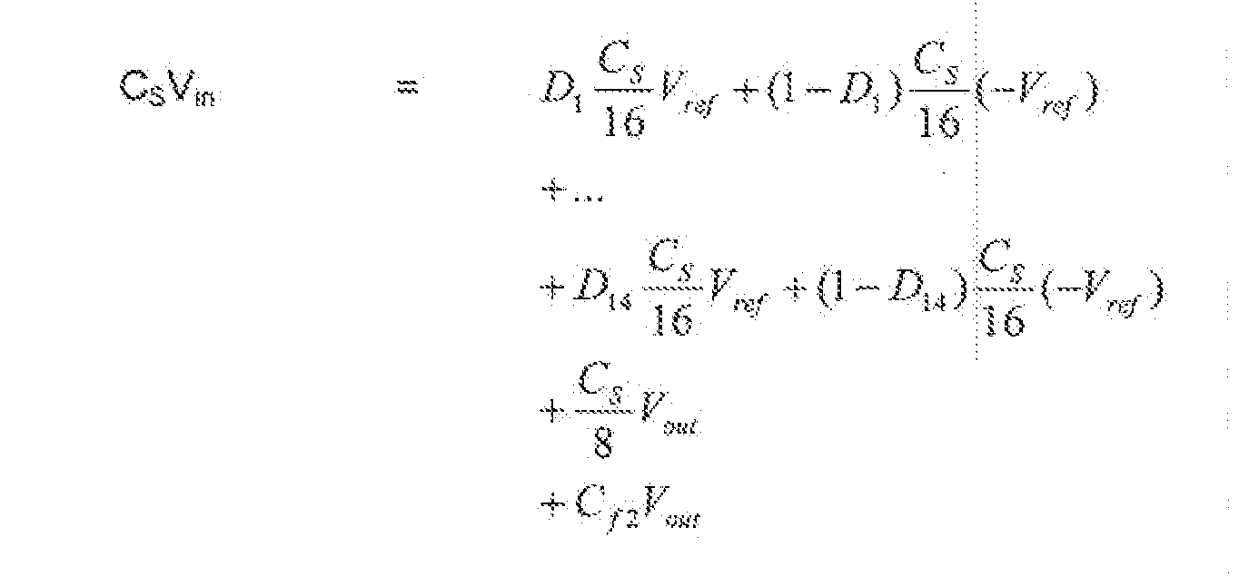
The input to output relationship of the MDAC circuit 40 shown in figure 3 is therefore:
The value of second feedback capacitor 41 may be set to Cς/8 and the input to output relationship can then be written as:
Therefore MDAC circuit 40 may have a gain of 4 and a subtraction of the analogue input signal from the analogue representation of the encoded digital signal according to -(1-2D)Vref. The gain of MOAC circuit 40 is therefore half that of MOAC circuit 20. As in MDAC circuit 20, the analogue input signal is divided by 2N= 16 when sampling, but the residue voltage in MDAC circuit 40 is amplified by 4. Therefore, including redundancy, the input range of MDAC circuit 40 is scaled down by a factor 2.
Therefore MDAC circuit 40 results in a range scaling of the input range to output range by a factor of 2.
It will be appreciated that through selection of alternative values of second feedback capacitor 41 , different gains may be realised using MDAC circuit 40.
The connection of second feedback capacitor 41 in a feedback configuration across operational amplifier 26 increases the value of and therefore increases
 the feedback factor of the MDAC circuit 40.
The speed of the circuit is characterized by its ~3d8-frequency
 where QBW is the gain-bandwidth product of the amplifier. The speed thus is proportional to the feedback factor, making a high feedback factor desirable.
The feedback factor of MDAC circuit 40 can be calculated as:


MOAC circuit 40 therefore exhibits an increased feedback factor over MOAC circuit 20. This results in a shorter settling time of the MOAC circuit
The sum of capacitance values of the first feedback capacitor 22 and the sampling capacitors should be equal to C, for the MOAC stage to perform the required functions of sampling, digital to analogue conversion, differencing and amplification. The same effect as described above could not therefore be achieved simply by increasing the size of the first feedback capacitor 22.
in switched-capacitor MDAC circuits the setting speed is proportional to the feedback factor. This invention describes an MDAC circuit using an N-bit ADSC, capable of realising various required gains, and with an up to 20% speed improvement as compared to typical MDAC circuits.
Shown in figure 5 is an alternative embodiment of an MOAC circuit 50 according to the invention, in which the inverting input 35a of the operational amplifier 26 is instead switchably connected to a fixed voltage node 51. The second plate 43 of the second feedback capacitor 41 is also switchably connected to the same fixed voltage node. The operation of the circuit in figure 5 is essentially identical to that of figure 4, as described above, with the only difference being that the second feedback capacitor 41 is discharged directly to the fixed voltage node 51 via switch 44.
In other alternative embodiments, switch 27 may be connected between the inverting 35a and non-inverting 35b inputs of the operational amplifier.
As described above in relation to the embodiments shown in figures 4 and 5. the range-scaling function of the MDAC is implemented with an additional second feedback capacitor 41. When the value of this capacitor equals Ca/8, and the open-loop gain Ao. of the operational amplifier 26 is high, the signal range of the output is scaled by a factor
of 2 compared with the input. The introduction of the second feedback capacitor requires some attention to be paid to maintain linearity. A non-linear portion of the charge sampled by the total input capacitance C, is transferred to the second feedback capacitor 41. When the input capacitance is reconnected to the input to acquire the next sample, its remaining charge couid cause distortion due to inter-symbol interference (ISI). in order to avoid this, a charge-reset switch arrangement 61 can be implemented in the pipeline stage circuit 60, as shown in figure 6. The circuit 60 of figure 6 is otherwise similar to the circuit shown in figure 4. The charge-reset switch arrangement 61 comprises a plurality of switches, each switch connected between a plate of each of the sampling capacitors 22, 21 and a fixed voltage node 62. which may be held at ground or a fixed voltage supply.
Figure 7 shows an exemplary timing diagram for the switches 61 of figure 6.
Operation (i.e. closing) of the switches 61 is triggered by a dock signal R, causing the input capacitors to be reset A further clock signal φ,R then causes the input witches to close, shortly after the switches 61 are opened. The remaining operation of the circuit 60 is similar to that described above in relation to figure 4.
Adding the charge-reset switching arrangement 61 to the input stage of the circuit 60 avoids the neeά for a dummy input sampling capacitance (for example as disclosed by P. Bogner et al., in "A 14b 100MS/S digitally self-calibrated pipelined AOC in 0.13μm
CMOS." ISSCC Dig. Tech. Papers, pp. 224-225, Feb. 2006}, thereby saving a significant amount of power needed to drive the capacitive loading on the circuit
The invention may be applied in the design of 14-bit 125-MS/s ADCs for highspeed analogue-to-digital and digital-to-anaiogυe conversion. Future products possibly incorporating the invention are e.g. a standalone 14-bit ADC for communication infrastructure and an embedded 12-bit ADC for consumer products.
Other embodiments are intentionally within the scope of the invention, as defined by the appended claims.
Claims
1. A multiplying digital-to-analogue converter circuit for a stage of a pipelined analogue-to-digital converter, the multiplying digital-to-analogue circuit comprising: an operational amplifier, at least one sampling capacitor having a first plate connected to an input of the
a first feedback capacitor having a first plate connected to the input of the operational amplifier, a second plate of the at least one sampling capacitor and the first feedback capacitor being swKchably connected to an analogue signal input according to a first dock signal to permit sampling of an analogue signal. the second plate of the at least one sampling capacitor being additionally switchabiy connected to a reference voltage according to a second clock signal in combination with a digital input, the second plate of the first feedback capacitor being switchabiy connected to an output of the operational amplifier according to the second clock signal; and a second feedback capacitor having a first plate connected to the input to the operational amplifier, and a second plate switchabiy connected to the input of the operational amplifier according to the first clock signal, the second plate being switchabiy connected to the output of the operational amplifier according to the second clock signal.
2. The multiplying digital-to-analogue converter circuit of ciaim 1 , wherein the input of the operational amplifier is switchabiy connected to a fixed voltage node according to a third dock signal.
3. The multiplying digital-to-analogue converter αrcuit of claim 1 wherein the non-inverting and inverting inputs of the operational amplifier are switchabiy connected together according to a third clock signal.
4. The multiplying digital-to-analogue converter circuit of claim 1 wherein the second plate of the second feedback capacitor is switchabiy connected directly to the input of the operational amplifier according to the first clock signal.
5. The multiplying digital-to-analogue converter circuit of claim 2 wherein the second plate of the second feedback capacitor is switchabiy connected to the fixed voltage node according to the first dock signal.
6. The multiplying digital-to-anaiogue converter circuit of claim 1 including a plurality of sampling capacitors arranged in parallel, each sampling capacitor corresponding to a bit of the digital signal input.
7. The multiplying digital-to-analogue converter circuit of claim 6 wherein the value of each of the sampling capacitors is the same.
8. The multiplying digital-to-analogue converter circuit of claim 6 wherein the values of the sampling capacitors are binary weighted.
9. The multiplying digital-to-analogue converter circuit of any preceding claim wherein the value of the first feedback capacitor and the second feedback capacitor are the same.
10. The multiplying digital-to-analogue converter circuit of any preceding claim wherein the first plate of each of the at least one sampling capacitor is switchabiy connected to a fixed voltage node according to a third clock signal.
11. A pipelined analogue-to-digital converter including a multiplying digital-to- analogυe converter circuit according to any preceding claim.
12. A method for providing an amplified residue voltage in a stage of a pipelined analogue-to-digitaf converter using a multiplying digital-to-analogue converter circuit according to claim 1 , the method comprising the steps of: a) sampling an analogue signal presented at the analogue signal input of the circuit; b) holding a charge corresponding to an instantaneous value of the sampled analogue signal on the second plate of the at least one sampling capacitor; c) differencing the sampled analogue signal with an analogue representation of a digital signal presented to the circuit to provide a residue voltage; and d) amplifying the residue voltage to provide an output signal to a further stage of a pipelined analogue-to-digital converter.
Applications Claiming Priority (2)
| Application Number | Priority Date | Filing Date | Title |
|---|---|---|---|
| EP08104422.4 | 2008-06-16 | ||
| EP08104422 | 2008-06-16 |
Publications (1)
| Publication Number | Publication Date |
|---|---|
| WO2010004456A1 true WO2010004456A1 (en) | 2010-01-14 |
Family
ID=41151806
Family Applications (1)
| Application Number | Title | Priority Date | Filing Date |
|---|---|---|---|
| PCT/IB2009/052497 Ceased WO2010004456A1 (en) | 2008-06-16 | 2009-06-11 | Digital-to-analogue converter |
Country Status (1)
| Country | Link |
|---|---|
| WO (1) | WO2010004456A1 (en) |
Citations (7)
| Publication number | Priority date | Publication date | Assignee | Title |
|---|---|---|---|---|
| US5499027A (en) * | 1994-02-24 | 1996-03-12 | Massachusetts Institute Of Technology | Digitally self-calibrating pipeline analog-to-digital converter |
| EP0899884A2 (en) * | 1997-07-31 | 1999-03-03 | Asahi Kasei Microsystems Co., Ltd. | D/A converter and delta-sigma D/A converter |
| JP2004336197A (en) * | 2003-05-01 | 2004-11-25 | Canon Inc | Analog-to-digital converter |
| US7102557B1 (en) * | 2005-04-19 | 2006-09-05 | Wolfson Microelectronics Plc | Switched capacitor DAC |
| US20070290915A1 (en) * | 2006-05-31 | 2007-12-20 | Renesas Technology Corp. | Pipeline A/D converter conterting analog signal to digital signal |
| US20070290914A1 (en) * | 2006-06-16 | 2007-12-20 | Matsushita Electric Industrial Co., Ltd. | A/d converter |
| US20080018514A1 (en) * | 2006-07-19 | 2008-01-24 | Samsung Electronics Co., Ltd. | Pipelined analog-to-digital converter and method of analog-to-digital conversion |
-
2009
- 2009-06-11 WO PCT/IB2009/052497 patent/WO2010004456A1/en not_active Ceased
Patent Citations (7)
| Publication number | Priority date | Publication date | Assignee | Title |
|---|---|---|---|---|
| US5499027A (en) * | 1994-02-24 | 1996-03-12 | Massachusetts Institute Of Technology | Digitally self-calibrating pipeline analog-to-digital converter |
| EP0899884A2 (en) * | 1997-07-31 | 1999-03-03 | Asahi Kasei Microsystems Co., Ltd. | D/A converter and delta-sigma D/A converter |
| JP2004336197A (en) * | 2003-05-01 | 2004-11-25 | Canon Inc | Analog-to-digital converter |
| US7102557B1 (en) * | 2005-04-19 | 2006-09-05 | Wolfson Microelectronics Plc | Switched capacitor DAC |
| US20070290915A1 (en) * | 2006-05-31 | 2007-12-20 | Renesas Technology Corp. | Pipeline A/D converter conterting analog signal to digital signal |
| US20070290914A1 (en) * | 2006-06-16 | 2007-12-20 | Matsushita Electric Industrial Co., Ltd. | A/d converter |
| US20080018514A1 (en) * | 2006-07-19 | 2008-01-24 | Samsung Electronics Co., Ltd. | Pipelined analog-to-digital converter and method of analog-to-digital conversion |
Non-Patent Citations (2)
| Title |
|---|
| BOGNER P: "A 28mW 10b 80MS/s pipelined ADC in 0.13[mu]m CMOS", PROCEEDINGS - IEEE INTERNATIONAL SYMPOSIUM ON CIRCUITS AND SYSTEMS - 2004 IEEE INTERNATIONAL SYMPOSIUM ON CIRCUITS AND SYSTEMS - PROCEEDINGS; VOLUME I OF V: ANALOG SIGNAL PROCESSING 2004 INSTITUTE OF ELECTRICAL AND ELECTRONICS ENGINEERS INC. US, vol. 1, 2004, pages I17 - I20, XP002551101 * |
| DATABASE INSPEC [online] THE INSTITUTION OF ELECTRICAL ENGINEERS, STEVENAGE, GB; 2000, HUI LIU ET AL: "Components of a 12-bit 50 Ms/s non-radix 2 pipeline analog-to-digital converter", XP002551102, Database accession no. 7145791 * |
Similar Documents
| Publication | Publication Date | Title |
|---|---|---|
| US5710563A (en) | Pipeline analog to digital converter architecture with reduced mismatch error | |
| US9954549B2 (en) | Charge-sharing and charge-redistribution DAC and method for successive approximation analog-to-digital converters | |
| EP0749205B1 (en) | Switched capacitor gain stage | |
| US8159382B2 (en) | Low power converter and shutdown SAR ADC architecture | |
| US8643529B2 (en) | SAR assisted pipelined ADC and method for operating the same | |
| US7852254B1 (en) | 1-bit cell circuit used in a pipelined analog to digital converter | |
| CN102484479A (en) | Switched capacitor circuit and stage circuit for ad converter | |
| EP1638208A1 (en) | Switched-capacitor circuit and pipelined A/D converter | |
| CN116366061A (en) | Pipelined successive approximation analog-to-digital converter based on switched load capacitor | |
| US8018361B2 (en) | Area-efficient analog-to-digital converter | |
| KR100810793B1 (en) | Nested pipelined analog-to-digital converter | |
| CN112511167A (en) | Low noise analog-to-digital converter | |
| US7821436B2 (en) | System and method for reducing power dissipation in an analog to digital converter | |
| US7034737B1 (en) | Switched capacitor circuits | |
| US7573417B2 (en) | Multi-bit per stage pipelined analog to digital converters | |
| US8451161B2 (en) | Switched-capacitor pipeline stage | |
| WO2010004456A1 (en) | Digital-to-analogue converter | |
| CN102790619B (en) | Switched Capacitor Circuit and Pipelined Analog-to-Digital Converter | |
| CN111147077B (en) | Gain calibration device and method for residual amplifier of analog-digital converter | |
| KR100888262B1 (en) | Signal Converters and Signal Conversion Methods | |
| CN113839675A (en) | Pipelined analog-to-digital converter based on non-50% duty cycle sampling clock | |
| Lee et al. | A 10-bit 100MS/s pipelined ADC in 0.18 μm CMOS technology | |
| Roy et al. | A parallel pipeline ADC with a Sub-ADC employing an improvized dynamic comparator | |
| Lu et al. | A 1.5 V 12-b 40 MSamples/s CMOS pipelined ADC | |
| Rydholm | Analysis of noise and offset in the comparator of ananalog-to-digital converter |
Legal Events
| Date | Code | Title | Description |
|---|---|---|---|
| 121 | Ep: the epo has been informed by wipo that ep was designated in this application |
Ref document number: 09786422 Country of ref document: EP Kind code of ref document: A1 |
|
| NENP | Non-entry into the national phase |
Ref country code: DE |
|
| 122 | Ep: pct application non-entry in european phase |
Ref document number: 09786422 Country of ref document: EP Kind code of ref document: A1 |