WO2010001497A1 - Semiconductor die pickup apparatus and semiconductor die pickup method - Google Patents
Semiconductor die pickup apparatus and semiconductor die pickup method Download PDFInfo
- Publication number
- WO2010001497A1 WO2010001497A1 PCT/JP2008/064516 JP2008064516W WO2010001497A1 WO 2010001497 A1 WO2010001497 A1 WO 2010001497A1 JP 2008064516 W JP2008064516 W JP 2008064516W WO 2010001497 A1 WO2010001497 A1 WO 2010001497A1
- Authority
- WO
- WIPO (PCT)
- Prior art keywords
- semiconductor die
- lid
- holding sheet
- stage
- contact surface
- Prior art date
Links
Images


Classifications
-
- H—ELECTRICITY
- H01—ELECTRIC ELEMENTS
- H01L—SEMICONDUCTOR DEVICES NOT COVERED BY CLASS H10
- H01L21/00—Processes or apparatus adapted for the manufacture or treatment of semiconductor or solid state devices or of parts thereof
- H01L21/67—Apparatus specially adapted for handling semiconductor or electric solid state devices during manufacture or treatment thereof; Apparatus specially adapted for handling wafers during manufacture or treatment of semiconductor or electric solid state devices or components ; Apparatus not specifically provided for elsewhere
- H01L21/683—Apparatus specially adapted for handling semiconductor or electric solid state devices during manufacture or treatment thereof; Apparatus specially adapted for handling wafers during manufacture or treatment of semiconductor or electric solid state devices or components ; Apparatus not specifically provided for elsewhere for supporting or gripping
- H01L21/6835—Apparatus specially adapted for handling semiconductor or electric solid state devices during manufacture or treatment thereof; Apparatus specially adapted for handling wafers during manufacture or treatment of semiconductor or electric solid state devices or components ; Apparatus not specifically provided for elsewhere for supporting or gripping using temporarily an auxiliary support
-
- H—ELECTRICITY
- H01—ELECTRIC ELEMENTS
- H01L—SEMICONDUCTOR DEVICES NOT COVERED BY CLASS H10
- H01L21/00—Processes or apparatus adapted for the manufacture or treatment of semiconductor or solid state devices or of parts thereof
- H01L21/67—Apparatus specially adapted for handling semiconductor or electric solid state devices during manufacture or treatment thereof; Apparatus specially adapted for handling wafers during manufacture or treatment of semiconductor or electric solid state devices or components ; Apparatus not specifically provided for elsewhere
- H01L21/67005—Apparatus not specifically provided for elsewhere
- H01L21/67011—Apparatus for manufacture or treatment
- H01L21/67132—Apparatus for placing on an insulating substrate, e.g. tape
-
- H—ELECTRICITY
- H01—ELECTRIC ELEMENTS
- H01L—SEMICONDUCTOR DEVICES NOT COVERED BY CLASS H10
- H01L21/00—Processes or apparatus adapted for the manufacture or treatment of semiconductor or solid state devices or of parts thereof
- H01L21/67—Apparatus specially adapted for handling semiconductor or electric solid state devices during manufacture or treatment thereof; Apparatus specially adapted for handling wafers during manufacture or treatment of semiconductor or electric solid state devices or components ; Apparatus not specifically provided for elsewhere
- H01L21/683—Apparatus specially adapted for handling semiconductor or electric solid state devices during manufacture or treatment thereof; Apparatus specially adapted for handling wafers during manufacture or treatment of semiconductor or electric solid state devices or components ; Apparatus not specifically provided for elsewhere for supporting or gripping
- H01L21/6835—Apparatus specially adapted for handling semiconductor or electric solid state devices during manufacture or treatment thereof; Apparatus specially adapted for handling wafers during manufacture or treatment of semiconductor or electric solid state devices or components ; Apparatus not specifically provided for elsewhere for supporting or gripping using temporarily an auxiliary support
- H01L21/6836—Wafer tapes, e.g. grinding or dicing support tapes
-
- H—ELECTRICITY
- H01—ELECTRIC ELEMENTS
- H01L—SEMICONDUCTOR DEVICES NOT COVERED BY CLASS H10
- H01L2221/00—Processes or apparatus adapted for the manufacture or treatment of semiconductor or solid state devices or of parts thereof covered by H01L21/00
- H01L2221/67—Apparatus for handling semiconductor or electric solid state devices during manufacture or treatment thereof; Apparatus for handling wafers during manufacture or treatment of semiconductor or electric solid state devices or components; Apparatus not specifically provided for elsewhere
- H01L2221/683—Apparatus for handling semiconductor or electric solid state devices during manufacture or treatment thereof; Apparatus for handling wafers during manufacture or treatment of semiconductor or electric solid state devices or components; Apparatus not specifically provided for elsewhere for supporting or gripping
- H01L2221/68304—Apparatus for handling semiconductor or electric solid state devices during manufacture or treatment thereof; Apparatus for handling wafers during manufacture or treatment of semiconductor or electric solid state devices or components; Apparatus not specifically provided for elsewhere for supporting or gripping using temporarily an auxiliary support
- H01L2221/68318—Auxiliary support including means facilitating the separation of a device or wafer from the auxiliary support
- H01L2221/68322—Auxiliary support including means facilitating the selective separation of some of a plurality of devices from the auxiliary support
-
- H—ELECTRICITY
- H01—ELECTRIC ELEMENTS
- H01L—SEMICONDUCTOR DEVICES NOT COVERED BY CLASS H10
- H01L2221/00—Processes or apparatus adapted for the manufacture or treatment of semiconductor or solid state devices or of parts thereof covered by H01L21/00
- H01L2221/67—Apparatus for handling semiconductor or electric solid state devices during manufacture or treatment thereof; Apparatus for handling wafers during manufacture or treatment of semiconductor or electric solid state devices or components; Apparatus not specifically provided for elsewhere
- H01L2221/683—Apparatus for handling semiconductor or electric solid state devices during manufacture or treatment thereof; Apparatus for handling wafers during manufacture or treatment of semiconductor or electric solid state devices or components; Apparatus not specifically provided for elsewhere for supporting or gripping
- H01L2221/68304—Apparatus for handling semiconductor or electric solid state devices during manufacture or treatment thereof; Apparatus for handling wafers during manufacture or treatment of semiconductor or electric solid state devices or components; Apparatus not specifically provided for elsewhere for supporting or gripping using temporarily an auxiliary support
- H01L2221/68327—Apparatus for handling semiconductor or electric solid state devices during manufacture or treatment thereof; Apparatus for handling wafers during manufacture or treatment of semiconductor or electric solid state devices or components; Apparatus not specifically provided for elsewhere for supporting or gripping using temporarily an auxiliary support used during dicing or grinding
- H01L2221/68336—Apparatus for handling semiconductor or electric solid state devices during manufacture or treatment thereof; Apparatus for handling wafers during manufacture or treatment of semiconductor or electric solid state devices or components; Apparatus not specifically provided for elsewhere for supporting or gripping using temporarily an auxiliary support used during dicing or grinding involving stretching of the auxiliary support post dicing
Definitions
- the present invention relates to a structure of a pickup device for a semiconductor die and a pickup method.
- the semiconductor die is manufactured by cutting a wafer having a size of 6 inches or 8 inches into a predetermined size. At the time of cutting, an adhesive holding tape is attached to the back surface so that the cut semiconductor dies do not fall apart, and the wafer is cut from the front side with a dicing saw or the like. At this time, the holding tape attached to the back surface is slightly cut, but is not cut and holds each semiconductor die. Each cut semiconductor die is picked up from the holding tape one by one and sent to the next process such as die bonding.
- this method using the push-up needle has a problem that the semiconductor die is broken by the push-up when the thickness of the semiconductor die is reduced, and it has become difficult to use it for the pickup of a thin semiconductor die in recent years. .
- Patent Document 1 a semiconductor die to be picked up is placed on a suction hole of a stage having a plurality of suction holes, and the suction hole is held in a vacuum while the semiconductor die is sucked and held on a collet. The sheet is sucked into each suction hole, deformed, the part of the holding sheet corresponding to the suction hole is peeled off from the semiconductor die, and then the stage is moved or rotated to hold the remaining part without being peeled off. There has been proposed a method of peeling a sheet from a semiconductor die (see FIGS. 1 to 4 of Patent Document 1).
- Patent Document 1 a protrusion having a narrower width than the semiconductor die to be picked up is provided on the surface of the stage, a suction hole is provided in the stage surface around the protrusion, and the semiconductor die is picked up.
- the semiconductor die to be picked up on the projecting part is placed so as to protrude from the projecting part, and is sucked and held by a collet, and the holding sheet of the part protruding from the projecting part is vacuum-sucked by the suction hole and the semiconductor sheet is held out of the projecting part.
- Patent Document 1 The method described in Patent Document 1 is a method in which the suction hole is evacuated, the holding tape is sucked into the suction hole, and the holding tape is peeled off from the semiconductor die. Since the surface is covered, air cannot be sucked from the portion around the suction hole after the holding tape just above the suction hole is peeled off. For this reason, the holding sheet directly above the suction hole can be peeled off by suction, but the portion around the suction hole cannot be peeled off by vacuum suction of the suction hole and remains in a state of being adhered to the semiconductor die. (See FIGS. 1 and 2 of Patent Document 1).
- the stage when the stage is moved to separate the peeled remaining portion of the holding sheet, the smaller the area of the remaining portion, the less the force applied to the semiconductor die, and the damage to the semiconductor die can be suppressed.
- the suction hole in order to reduce the remaining portion to be peeled off by the suction hole, it is necessary to make the suction hole large in accordance with the size of the semiconductor to be picked up. If the holding sheet is sucked at once by such a large suction hole, a large force may be applied to the semiconductor die when the adhesive force of the holding sheet is large.
- recent semiconductor dies are thin and low in strength, and this force may cause cracking or deformation.
- Patent Document 1 Another method described in Patent Document 1 is to evacuate a small suction hole arranged only around the protruding portion to peel off the portion of the semiconductor die holding sheet protruding from the protruding portion, Because the holding sheet of the semiconductor die is peeled off by the tensile force applied to the holding sheet, it is necessary to increase the height of the protruding part in order to reliably peel off the holding sheet. If there is a semiconductor die adjacent in the direction, the protrusion may hit the semiconductor die and damage the semiconductor die, so the height of the protrusion is limited and the holding sheet cannot be peeled off reliably. There was a problem.
- an object of the present invention is to easily pick up a semiconductor die while suppressing a force applied to the semiconductor die when the holding sheet is peeled off in a semiconductor die pickup apparatus.
- the semiconductor die pick-up device of the present invention is a semiconductor die pick-up device for picking up a semiconductor die attached to a holding sheet, and is in close contact with the surface of the holding sheet opposite to the surface to which the semiconductor die is attached.
- a cylindrical stage including a close contact surface, a suction opening provided on the close contact surface and extending in a straight line from the inner periphery side to the outer periphery side of the stage with substantially the same width as the semiconductor die to be picked up, and the width of the suction opening It is provided on the stage so that the tip on the side that closes the suction opening can move forward from the contact surface with approximately the same width, slide along the contact surface to open and close the suction opening, and let the tip of the lid advance from the contact surface
- the surface that pushes up the holding sheet of the lid is inclined downward from the front end side of the lid toward the rear end side of the lid opening side, and is recessed from the contact surface by the thickness of the lid.
- the inclination angle of the inclined surface with respect to the contact surface is preferably larger than the inclination angle with respect to the contact surface of the surface opposite to the surface that pushes up the holding sheet of the lid, A step portion extending from the inclined surface to the outer peripheral surface of the stage along the contact surface is provided. It is also preferable that the inclination angle is larger than the inclination angle of the contact surface, and the inclination surface is also preferably a plane substantially perpendicular to the contact surface.
- a pin is provided that extends in the width direction of the suction opening, and includes a slider that slides in the direction in which the suction opening extends by a slider drive mechanism provided inside the stage and moves forward and backward with respect to the contact surface. It is also preferable that the lid includes an arm projecting from the tip to the side of closing the suction opening and is rotatably attached to the slider pin via the arm.
- the semiconductor die pick-up method of the present invention is a semiconductor die pick-up method for picking up a semiconductor die attached to a holding sheet, wherein the semiconductor die of the holding sheet to which the semiconductor die to be picked up is attached is attached.
- a cylindrical stage including a contact surface that is in close contact with the surface opposite to the surface on which it is located, and a linear surface extending from the inner periphery side of the stage toward the outer periphery side with the same width as the semiconductor die to be picked up, provided on the contact surface
- the suction opening and the width of the suction opening are substantially the same width, provided on the stage so that the tip of the suction opening closing side can be advanced from the contact surface, slide along the contact surface to open and close the suction opening, When the front end of the lid is advanced from the contact surface, the surface that pushes up the holding sheet of the lid is inclined downward from the front end side of the lid toward the rear end side of the lid opening side.
- a semiconductor die pick-up device comprising a collet for adsorbing the die is prepared, one end of the semiconductor die to be picked up is aligned with the tip of the closed lid, and the width direction position of the lid and the width direction position of the semiconductor die are Alignment process, the tip of the lid is advanced from the contact surface, the holding sheet and the semiconductor die are pushed up, and the surface on the opposite side of the lid from which the holding sheet is pushed up is inclined with the bottom surface of the slide groove Slide the lid from one end to the other end of the semiconductor die to be picked up while making contact with the edge with the surface to open the suction openings sequentially, and pick up the open suction opening from one end of the semiconductor die to the other end.
- the holding sheet is sequentially sucked toward and picked up from the semiconductor die to be picked up sequentially, and the semiconductor die is sequentially adsorbed from one end side to the other end side on the collet waiting immediately above the semiconductor die to be picked up, A pickup step of picking up a semiconductor die.
- the present invention provides an effect that a semiconductor die can be easily picked up while suppressing a force applied to the semiconductor die when the holding sheet is peeled off in the semiconductor die pick-up device.
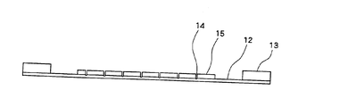
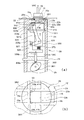
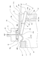
- an adhesive holding sheet 12 is attached to the back surface of the wafer 11, and the holding sheet 12 is attached to a metal ring 13.
- the wafer 11 is handled in such a state that it is attached to the metal ring 13 via the holding sheet 12 in this way.
- the wafer 11 is cut by a dicing saw or the like from the surface side into a semiconductor die 15 in the cutting process.
- a notch gap 14 formed during dicing is formed between the semiconductor dies 15. The depth of the cut gap 14 reaches from the semiconductor die 15 to a part of the holding sheet 12, but the holding sheet 12 is not cut and each semiconductor die 15 is held by the holding sheet 12.
- the wafer holder 10 includes an annular expand ring 16 having a flange portion and a ring presser 17 for fixing the ring 13 on the flange of the expand ring 16.
- the ring retainer 17 is driven in a direction to advance and retract toward the flange of the expand ring 16 by a ring retainer drive unit (not shown).
- the inner diameter of the expand ring 16 is larger than the diameter of the wafer on which the semiconductor die 15 is arranged, the expand ring 16 has a predetermined thickness, and the flange is outside the expand ring 16 and is separated from the holding sheet 12.
- the wafer holder 10 is configured to be movable in a direction along the surface of the holding sheet 12 by a wafer holder horizontal direction drive unit (not shown).
- the holding sheet 12 to which the semiconductor die 15 is attached is in a substantially planar state before being set on the expanding ring 16.
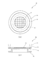
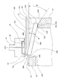
- FIG. 4 is a diagram showing a configuration of the semiconductor die pick-up apparatus 100, and FIG. 4 shows a state in which the semiconductor die 15 attached to the holding sheet 12 is set in the semiconductor die pick-up apparatus 100.
- the ring presser 17 is lowered on the ring 13, and the ring 13 is sandwiched between the flanges of the expand ring 16. Since there is a step between the upper surface where the holding sheet 12 of the expand ring 16 contacts and the flange surface, when the ring 13 is pressed against the flange surface, the holding sheet 12 is the same as the step between the upper surface of the expand ring 16 and the flange surface.
- the expansion ring 16 is stretched along the curved surface.
- the holding sheet 12 fixed on the expand ring 16 is subjected to a pulling force from the center of the holding sheet toward the periphery.
- a gap between the semiconductor dies 15 attached on the holding sheet 12 is widened.
- the wafer holder 10 is attached with a wafer holder horizontal direction driving unit 72 that moves the wafer holder 10 along a surface along the holding sheet 12.
- the wafer holder horizontal direction driving unit 72 may be, for example, a unit that drives the wafer holder 10 in the horizontal direction by a motor and a gear provided inside, or along a guide by a driving source such as a motor provided outside.
- the wafer holder 10 may be moved in the XY direction.
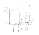
- a collet 18 for attracting and moving the semiconductor die 15 is provided on the wafer holder 10.
- the collet 18 includes suction holes 19 for sucking the semiconductor die 15 on the suction surface, and each suction hole 19 is connected to a vacuum device 71.
- a stage 20 is provided below the wafer holder 10, and the stage 20 is driven in a vertical direction that is an advancing / retreating direction with respect to the holding sheet 12 by a stage vertical direction driving mechanism 73.
- the stage vertical direction drive mechanism 73 may be, for example, a mechanism that drives the stage 20 in the vertical direction by a motor and a gear provided inside, or is vertically moved along a guide by a drive source such as a motor provided outside.
- the stage 20 may be moved in the direction.
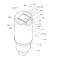
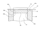
- the stage 20 has a cylindrical casing 21 having a close contact surface 22 in close contact with the holding sheet 12 on the upper surface thereof, and a base portion 24 provided on the opposite side of the close contact surface 22 of the casing 21. And a drive unit 25 that is attached to the base unit 24 and drives a slider drive mechanism 300 attached to the inside of the housing 21.
- the base portion 24 of the stage 20 is attached to a stage fixing portion (not shown).
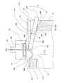
- the suction opening 41 is provided in the contact surface 22, is substantially the same width as the semiconductor die 15 to be picked up shown in FIG. 4, and is longer than the semiconductor die 15, from the inner peripheral side of the stage 20 toward the outer peripheral side. It extends in a straight line.
- a lid 23 that slides along the direction in which the suction opening 41 extends and opens and closes the suction opening 41 is attached to the suction opening 41.
- the side of the lid 23 that closes the suction opening 41 along the sliding direction is the front end 23a, and the end on the side where the lid 23 opens is the rear end 23c.
- the side surface 23b of the lid 23 and the side surface 41b of the suction opening 41 constitute a slide surface. If the suction opening 41 has substantially the same width as the semiconductor die 15 to be picked up on the contact surface 22, a step is provided inside, and a slit communicating with the stage 20 is provided in the step portion. May be.
- the tip 23a of the lid 23 is a curved surface that is convex toward the side of closing the suction opening 41, and the end surface 41 a of the suction opening against which the tip 23 a of the lid 23 is pressed has a curved surface along the curved surface of the tip 23 a of the lid 23.
- the curved surface may be a cylindrical surface, a combination of cylindrical surfaces having a plurality of radii, or a curved surface having another shape.
- a longitudinal groove 364 that extends in the direction and sucks the holding sheet 12 is provided.
- the vertical groove 364 is configured by a fan-shaped cylindrical surface of approximately 270 degrees connected to the suction opening 41, and the tangent line 500 that contacts the cylindrical surface of each vertical groove 364 at both corners of the suction opening 41 is the cylindrical surface of the end surface 41a. It protrudes from the end face 41a in the direction in which the lid 23 is closed to a position that becomes a tangent.
- a vertical groove 364 having a fan-shaped cylindrical surface of approximately 270 degrees communicates the contact surface 22 and the inside of the housing 21.
- 7B when the one end 15a of the semiconductor die 15 is aligned with the end face 41a of the suction opening 41 or the tip 23a of the lid 23, a part of the semiconductor die 15 is part of the tip of the lid 23.
- the fan-shaped hatched portion that protrudes from 23 a and is approximately 90 degrees is located above the vertical groove 364.
- the surface on the holding sheet 12 side becomes substantially flush with the contact surface 22.
- a chamfered portion 23 e is provided around the surface of the lid 23, and when the lid 23 closes the suction opening 41, a small V-shaped groove is formed between the contact surface 22 and the lid 23.
- the width of the suction opening 41, the width of the lid 23, and the width of the semiconductor die 15 are substantially the same, and the side surfaces 41b of the suction opening 41 and the side surfaces 23b of the lid 23 slide. It touches.
- the stage 20 is recessed from the contact surface 22 by the thickness of the lid 23, and is substantially the same width as the lid 23 from the end of the suction opening 41 on the side where the lid 23 opens to the outer peripheral side of the stage 20.
- An extending slide groove 22a and an inclined surface 22b following the bottom surface 22a 'of the slide groove 22a are provided.
- the side surface 22h of the slide groove 22a is the same surface as the side surface 41b of the suction opening 41, and the side surface 23b of the lid 23 and the side surface 22h of the slide groove 22a constitute a slide surface.
- the bottom surface 22 a ′ of the slide groove 22 a is substantially parallel to the contact surface 22 and does not cover the cylindrical surface of the outer periphery of the stage 20, and is more than the position of the rear end 23 c of the lid 23 when the lid 23 closes the suction opening 41. It extends to the end 22c located at the stage inner peripheral side.
- the end 22c is linear, and the rear end 23c of the lid 23 projects slightly toward the outer periphery of the stage 20 from the end 22c of the slide groove 22a with the lid 23 closed.
- the inclined surface 22b is inclined downward from the end 22c of the sliding groove 22a in the direction opposite to the contact surface 22. Side surfaces 22j that are flush with the side surface 22h of the sliding groove 22a extend on both sides of the inclined surface 22b.
- the side surface 22j and the side surface 23b of the lid 23 constitute a slide surface.
- a line of intersection between the inclined surface 22b and the bottom surface 22a 'of the slide groove 22a forms a linear ridge line edge 22d extending in a direction perpendicular to the slide direction of the lid 23.
- the rear end 23c of the lid 23 protrudes to the outer peripheral side of the stage 20 from the end 22c of the slide groove 22a and the edge 22d in a state where the lid 23 closes the suction opening 41.
- the lower surface 23g which is the surface opposite to the surface to be pushed up, is supported by the edge 22d.
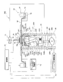
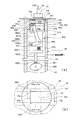
- a slider drive mechanism 300 for sliding a slider 332 to which a lid 23 is rotatably attached is provided inside the stage 20.
- the slider drive mechanism 300 is slidably attached to the first link 326 driven in the forward and backward direction with respect to the contact surface 22 by the drive unit 25 attached to the base portion 24 of the stage 20 and the housing 21 of the stage 20.
- a piston 370 that moves forward and backward with respect to the contact surface 22; a stopper 321a that is provided inside the housing 21 and that engages with a flange 371 of the piston 370 to limit the movement of the piston 370 in the forward / backward direction; A spring 373 that connects one link 326 and the piston 370 in a direction that advances and retreats with respect to the contact surface 22; a guide rail 331 that is attached to the piston 370 and extends substantially parallel to the contact surface 22 and extends in the direction of the suction opening 41; A slider 332 slidably attached to the guide rail 331 and a piston 370 can be freely rotated by a pin 328.
- a cylindrical pin 330 extending in the width direction of the suction opening 41 is attached to the slider 332, and an inverted U-shape provided on an arm 23 f that protrudes from the tip 23 a of the lid 23 toward the closing side of the suction opening 41.
- the mold notch is rotatably engaged.
- casing 21 is connected to the vacuum apparatus 71, and is comprised so that an inside can be made into a vacuum.
- the pin 327 provided at one end enters the engagement groove 326a of the first link 326, and the engagement groove 329a provided at the other end sandwiches the pin 330a of the slider 332, whereby the first link 326 and the first link 326 are engaged with the first link 326.
- a link 326 is connected.
- a motor 381 for operating the slider drive mechanism 300 is attached inside the drive unit 25, and a cam that contacts a roller 326 c provided at the tip of the shaft 326 b of the first link 326 on the rotating shaft of the motor 381. 383 is attached.
- the slider drive mechanism 300 changes the operation of the first link 326 that moves in the forward and backward direction toward the contact surface 22 to the operation in the direction in which the slider 332 is moved in parallel with the contact surface 22 by the L-shaped second link 329. Since it is converted, the structure can be made compact, and the mechanism can be stored inside the cylindrical casing 21.
- a semiconductor die pick-up device 100 includes a control unit 70 which is a computer including a CPU and the like, and includes a driving unit 25, a vacuum device 71, a collet 18, a wafer holder horizontal driving unit 72, a stage.
- the vertical drive mechanism 73 is connected to each other, and the drive unit 25, vacuum device 71, collet 18 and wafer holder horizontal drive unit 72, and stage vertical drive mechanism 73 are configured to be driven by commands output from the control unit 70.
- a one-dot chain line indicates a signal line that connects the control unit 70, the drive unit 25, the vacuum device 71, the collet 18, the wafer holder horizontal direction drive unit 72, and the stage vertical direction drive mechanism 73.
- FIGS. 1 to 8 The portions described with reference to FIGS. 1 to 8 are denoted by the same reference numerals, and description thereof is omitted.
- the control unit 70 starts the alignment process between the lid 23 and the semiconductor die 15 with the lid 23 closed. Since the lid 23 is in a position where the suction opening 41 is closed, the tip 23a of the lid 23 is in contact with the end surface 41a of the suction opening 41, and the lower surface of the rear end 23c of the lid 23 is the surface of the slide groove 22a. And is supported by the slide groove 22a. Further, the surface of the lid 23 and the contact surface 22 are substantially the same surface.
- the controller 70 moves the wafer holder 10 horizontally above the standby position of the stage 20 by the wafer holder horizontal direction driving unit 72 shown in FIG.
- the controller 70 once stops the horizontal movement of the wafer holder 10, and the stage 20 is brought into close contact with the stage vertical drive mechanism 73.
- the stage 20 is raised until the surface 22 and the surface of the lid 23 are in close contact with the lower surface of the holding sheet 12.
- the control unit 70 stops raising the stage 20.
- the control unit 70 again aligns the one end 15a of the semiconductor die 15 to be picked up with the tip 23a of the lid 23 in the closed state by the wafer holder horizontal direction driving unit 72, and the position in the width direction of the lid 23 and the position of the semiconductor die 15
- the width direction position is adjusted and adjusted so that the side surface of the semiconductor die 15 matches the side surface 23 b of the lid 23. Since the width of the lid 23 is substantially the same as that of the semiconductor die 15 to be picked up, the position of each side surface of the semiconductor die 15 and each side surface 23b of the lid 23 when the one side surface 23b is aligned with the side surface of the semiconductor die 15. Can be combined.
- the holding sheet 12 receives a tensile force by the expanding ring 16 of the wafer holder 10.
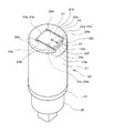
- FIG. 9B is a plan view of the contact surface 22 of the stage 20 and the surface of the lid 23.
- the holding sheet 12 and the semiconductor die 15 placed thereon are indicated by a one-dot chain line so that the positional relationship can be understood.
- the lid 23 is shown slightly larger than the semiconductor die 15 in order to distinguish between the semiconductor die 15 and the lid 23 having substantially the same width.
- FIGS. 10B and 12B As shown in FIG. 9 (b), when the positions of the lid 23 and the semiconductor die 15 are aligned, the approximately 90-degree fan-shaped hatched portion of the semiconductor die 15 is located on the vertical groove 364.
- the control unit 70 ends the alignment process. Then, the control unit 70 moves to the position immediately above the semiconductor die 15 from which the collet 18 is to be picked up, and holds the collet 18 at a height with a slight gap. When the movement of the collet 18 is finished, the control unit 70 starts sucking air from the suction hole 19 by the vacuum device 71, and puts the collet 18 in a suction standby state of the semiconductor die 15.
- the control unit 70 starts the holding sheet peeling process.
- the control unit 70 evacuates the inside of the casing 21 of the stage 20 using the vacuum device 71.
- the vertical groove 364 communicating with the inside of the housing 21 shown in FIG. 10B is also evacuated, and the holding sheet 12 is attracted to the contact surface 22.
- the holding sheet 12 is pulled downward by the vacuum, but in this state, the holding sheet 12 is not yet peeled from the semiconductor die 15.
- the V-shaped groove between the chamfered portion 23e provided on the surface of the lid 23 shown in FIG. 8 and the suction opening 41 air flows from the outer peripheral side of the stage 20 toward the vertical groove 364 that becomes a vacuum. Flowing.
- the pressure in the V-shaped groove is lower than the atmospheric pressure, but the holding sheet 12 is not peeled off at this negative pressure.
- the cam 383 attached to the shaft of the motor 381 is rotated.
- the cam 383 has an elliptical shape, and the cam surface is in contact with the roller 326c attached to the tip of the shaft 326b of the first link 326.
- the cam surface of the cam 383 becomes the roller 326c. Is pushed up toward the contact surface 22.
- the shaft 326 b rises and the entire first link 326 rises toward the contact surface 22.
- the tip 23 a of the lid 23 advances upward from the contact surface 22, the tip 23 a of the lid 23 pushes up the holding sheet 12 and one end 15 a of the semiconductor die 15. Then, since the tip 23 a receives a downward force from the holding sheet 12, the lid 23 rotates clockwise about the pin 330.
- the lower surface 23g which is the surface opposite to the surface that pushes up the holding sheet 12 of the lid 23, is supported by an edge 22d between the slide groove 22a and the inclined surface 22b, and the surface of the rear end 23c on the holding sheet 12 side is in close contact. Since the surface is substantially flush with the surface 22, the surface of the lid 23 that pushes up the holding sheet 12 is inclined downward from the front end 23a side of the lid 23 toward the rear end 23c side.
- the inclination angle is an angle ⁇ with respect to the contact surface 22.
- the inclined surface 22b is inclined with respect to the contact surface 22 by an angle ⁇ larger than the angle ⁇ . For this reason, the inclined surface 22b does not hinder the movement of the rear end 23c of the lid 23, and the lower surface 23g of the lid 23 is always in line contact with the edge 22d.
- the lid 23 pushes up the semiconductor die 15 and the holding sheet 12 to be picked up.
- the holding sheets 12 at both corners of the semiconductor die 15 located on the vertical grooves 364 that have become vacuum are sucked and fixed to the contact surface 22.
- the holding sheet 12 attached to the semiconductor die 15 to be picked up is pulled obliquely downward toward the contact surface 22, and the diagonal downward pulling force causes the holding sheet 12 to be placed on the vertical groove 364.
- the holding sheet 12 begins to peel from both corners of the semiconductor die 15 positioned, and the approximately 90-degree fan-shaped holding sheet 12 positioned on the longitudinal groove 364 is peeled off.
- the holding sheet 12 of the substantially triangular portion of the semiconductor die 15 that protrudes from the tip 23 a of the lid 23 to the contact surface 22 is pulled obliquely downward toward the contact surface 22.
- the semiconductor die 15 is peeled from both sides in the width direction toward the center in the width direction.
- the peeling line 53 is formed at a position slightly closer to the sliding direction of the lid 23 than the one end 15 a of the semiconductor die 15.
- the portion of the semiconductor die 15 from which the holding sheet 12 is peeled loses the force drawn toward the contact surface 22 by the holding sheet 12.
- the pressure on the surface of the semiconductor die 15 on the collet 18 side is reduced by approaching the adsorption surface of the collet 18 by the upward movement of the tip 23a of the lid 23.
- the pressure of the surface of the semiconductor die 15 on the holding sheet 12 side becomes higher than the pressure on the collet 18 side, and the portion of the semiconductor die 15 peeled off from the holding sheet 12 is adsorbed by the collet 18.
- a portion of the semiconductor die 15 on the rear end 23c side of the lid 23 from the peeling line 53 where the holding sheet 12 has not yet been peeled is left with a slight gap between the semiconductor die 15 and the collet 18. Since the pressure difference between the holding sheet 12 side and the collet 18 side is not so large and there is a pulling force by the holding sheet 12, it is not yet adsorbed by the collet 18. For this reason, the semiconductor die 15 undergoes minute bending deformation between a portion adsorbed by the collet 18 and a portion not adsorbed by the collet 18.
- the peeling line 53 is a line extending from the side surface in the width direction of the semiconductor die 15 to the side surface along the tip 23 a of the lid 23, and in the portion along the side surface 23 b of the lid 23.
- the peeling line 53 does not extend.
- each side surface 23b of the lid 23 is in contact with each side surface 41b of the suction opening 41. It has become a state.
- the lower surface of the rear end 23c of the lid 23 is in contact with the surface of the slide groove 22a.
- the holding sheet 12 peeled off from the semiconductor die 15 is covered on the vertical groove 364. For this reason, since almost no air flows from the outside of the housing 21 toward the inside of the housing 21, the inside of the housing 21 is kept in a vacuum.
- the spring 373 of the slider drive mechanism 300 has such a stiffness that it hardly bends when the tip 23 a of the lid 23 is pushed up from the contact surface 22, the tip 23 a of the lid 23 has a predetermined advance height from the contact surface 22. Even if pushed up, the distance between the piston 370 and the first link 326 hardly changes. For this reason, the lid 23 only protrudes from the contact surface 22 by the rising of the first link 326 and does not slide.
- the pin 328 of the piston 370 does not rise with respect to the contact surface 22, and only the pin 327 of the second link 329 entering the engagement groove 326 a of the first link 326 rises in the direction of the contact surface 22. Then, the second link 329 starts to rotate around the pin 328. By this rotation operation, the engaging groove 329a at the other end of the second link 329 moves toward the outer periphery of the stage 20, and the slider 332 and the pin of the slider 332 to which the pin 330a in the engaging groove 329a is fixed.
- the lid 23 that is rotatably engaged with the 330 via the arm 23 f starts to slide toward the outer peripheral side of the stage 20.
- the tip 23a of the lid 23 is separated from the end face 41a of the suction opening 41, and the suction opening 41 is opened to have an opening having substantially the same width as the semiconductor die 15 to be picked up.
- An opening 42 is formed. Since the inside of the housing 21 of the stage 20 is in a vacuum state by the vacuum device 71, the opening opening 42 sucks the holding sheet 12 therein. Then, the holding sheet 12 is drawn into the opening portion 42 as the lid 23 slides, and is peeled off from the semiconductor die 15.
- the center in the width direction of the lid 23 from the adhesion surface 22 is a ridge line that rises in a mountain shape.
- each side surface 23 b side of the lid 23 is a line inclined toward the sliding direction from the center portion. For this reason, the holding sheet 12 on each side of the semiconductor die 15 is peeled off before the holding sheet 12 at the center portion in the width direction of the semiconductor die 15.
- the peeling line 53 is inclined with respect to the ends 15a and 15b of the semiconductor die 15 or with respect to the sliding direction in the plane along the contact surface 22, the portion adsorbed by the collet 18 and the collet The stress generated by a minute bending deformation between the portion not adsorbed by 18 is relieved, and damage to the semiconductor die 15 can be effectively suppressed.
- the opening portion 42 increases toward the outer peripheral side of the stage 20, and the peeling line 53 sequentially moves in parallel to the outer peripheral side of the stage 20.
- the holding sheet 12 is sequentially peeled from the one end 15 a to the other end 15 b of the semiconductor die 15 along the peeling line 53, and is sequentially sucked into the opening opening 42.
- the lower surface 23g opposite to the surface pushing up the holding sheet 12 of the lid 23 slides in contact with the edge 22d.
- the tangent line of the lower surface 23g of 23 is a seal line that separates the outside of the casing 21 at atmospheric pressure from the inside of the casing 21 in a vacuum state.
- the side surface 23b of the lid 23, the side surface 22j of the slide groove 22a, and the side surfaces 22h on both sides of the lid 23 and the inclined surface 22b constitute a slide surface.
- the opening portion 42 is covered by the peeled holding sheet 12, but the holding sheet 12 is sucked into the opening portion 42, and the tip 23 a of the lid 23 faces the portion where the holding sheet 12 is not peeled off. Therefore, the suction of the holding sheet 12 by the opening 42 is not stopped, and the entire holding sheet 12 is sequentially sucked from the one end 15a of the semiconductor die 15 to the other end 15b by the opening 42. It can be peeled off and the remaining part of the peeling can be prevented.
- the semiconductor die 15 is entirely adsorbed by the collet 18 and picked up by the collet 18.
- the cam 383 of the slider drive mechanism 300 After the semiconductor die 15 is picked up, when the cam 383 of the slider drive mechanism 300 further rotates according to a command from the control unit 70, the shaft 326b of the first link 326 is lowered due to the rotation of the cam 383.
- the lid 23 closes the suction opening 41 when the tip 23a is in contact with the end face 41a, sliding in the direction toward the end face 41a of the suction opening 41. Then, the compression force of the spring 373 is released.
- the cam 383 further rotates and the shaft 326b is lowered, the piston 370, the first link 326, and the second link 329 are both lowered, and the tip 23a of the lid 23 is lowered to substantially the same position as the surface of the contact surface 22. To return to the initial position.
- the lid 23 is slid in a state in which the tip 23a of the lid 23 is advanced upward from the contact surface 22, and substantially the same width as that of the semiconductor die 15 appearing immediately below the semiconductor die 15.
- the holding sheet 12 is sequentially pulled into the opening portion 42 of the suction opening 41 to sequentially peel off the holding sheet 12, and the semiconductor die 15 is sequentially placed on the collet 18 waiting immediately above the semiconductor die 15. Since the adsorption is performed, the semiconductor die 15 can be easily picked up while suppressing the force applied to the semiconductor die 15 when the holding sheet 12 is peeled off.
- the tip 23a of the lid 23 is advanced upward from the contact surface 22 in a state where the vertical groove 364 is evacuated, and the semiconductor die 15 is pushed up and picked up by the downward pulling force generated in the holding sheet 12. Since a trigger for peeling is created by peeling off the holding sheets 12 at both corners of the one end 15a of the semiconductor die 15, and then the lid 23 is slid to suck the holding sheet 12 into the opening 42, There is an effect that the holding sheet 12 can be peeled off more easily.
- the lid 23 is slid from the one end 15a side to the other end 15b side of the semiconductor die 15, and the holding sheet 12 is sequentially sucked into the opening opening 42 to peel off the holding sheet 12. Even if the opening portion 42 is covered by the holding sheet 12 sucked into the opening portion 42, the lid 23 slides toward the portion where the holding sheet 12 is not peeled, so that the entire holding sheet 12 is sequentially opened. The opening 42 can be sucked and peeled off, and the entire holding sheet 12 can be easily peeled off.
- the tip 23 a of the lid 23 is a curved surface
- the peeling line 53 is inclined with respect to the ends 15 a and 15 b of the semiconductor die 15 or with respect to the sliding direction within the plane along the contact surface 22.
- the part that advances upward from the contact surface 22 is a part of the vicinity of the tip 23a of the lid 23, and the rear end 23c of the lid 23 does not advance upward from the contact surface 22, so that the lid 23 is slid.
- the rear end 23c of the lid 23 does not collide with the adjacent semiconductor die 15, and the adjacent semiconductor die 15 is not damaged by the sliding of the lid 23. Therefore, even when there are adjacent semiconductor dies 15 around The semiconductor die 15 can be picked up.
- the stage 20 includes only a vertical movement in the advancing and retreating direction with respect to the holding sheet 12 by the stage vertical driving mechanism 73, and a moving mechanism with respect to the horizontal direction that is along the holding sheet 12. Therefore, there is no backlash of the mechanism in the horizontal direction, and the position stability in the direction along the holding sheet 12 is good. Further, since the alignment of the semiconductor die 15 to be picked up and the lid 23 in the direction along the surface of the holding sheet 12 is performed by the wafer holder horizontal direction driving unit 72, the horizontal position of the stage 20 is adjusted during the horizontal alignment. Is stable, and it is possible to reduce the occurrence of misalignment during alignment between the lid 23 of the stage 20 and the semiconductor die 15 attached to the holding sheet 12.
- FIGS. 1 to 13 Parts similar to those of the embodiment described with reference to FIGS. 1 to 13 are denoted by the same reference numerals and description thereof is omitted.
- the stage 20 is recessed from the contact surface 22 by the thickness of the lid 23, from the end of the suction opening 41 on the side where the lid 23 opens with substantially the same width as the lid 23 toward the outer peripheral side of the stage 20.
- the bottom surface 22a 'of the slide groove 22a a flat surface 22e substantially perpendicular to the contact surface 22 and a step portion 22f are provided.
- the side surface 22h of the slide groove 22a is the same surface as the side surface 41b of the suction opening 41, and the side surface 23b of the lid 23 and the side surface 22h of the slide groove 22a constitute a slide surface.
- the bottom surface 22a ′ of the slide groove 22a is substantially parallel to the contact surface 22 and does not cover the cylindrical surface on the outer periphery of the stage 20, and from the position of the rear end 23c of the lid 23 with the lid 23 closing the suction opening 41. Also extends to the end 22c at the position on the inner periphery side of the stage.
- the end 22c is linear, and the rear end 23c of the lid 23 protrudes slightly to the outer peripheral side of the stage 20 from the end 22c of the slide groove 22a with the lid 23 closed.
- the flat surface 22e extends vertically from the end 22c of the slide groove 22a in the direction opposite to the contact surface 22 and downward in the longitudinal direction of the housing 21.
- An intersection line between the flat surface 22e and the bottom surface 22a 'of the slide groove 22a forms an edge 22d of a linear ridge line extending in a direction perpendicular to the sliding direction of the lid 23.
- the flat surface 22e continues to a step 22f extending from the flat surface 22e to the outer peripheral surface of the housing 21 substantially in parallel with the contact surface 22. Since the step 22 f extends to the outer peripheral surface of the cylindrical casing 21, the outer peripheral end 22 g is an arc along the cylinder of the casing 21.
- Side surfaces 22j that are flush with the side surface 22h of the slide groove 22a extend on both sides of the step 22f.
- the side surface 22j and the side surface 23b of the lid 23 constitute a slide surface.
- the rear end 23c of the lid 23 protrudes to the outer peripheral side of the stage 20 from the end 22c of the slide groove 22a and the edge 22d in a state where the lid 23 closes the suction opening 41.
- the lower surface 23g which is the surface opposite to the surface to be pushed up, is supported by the edge 22d.
- the angle of the surface including the edge 22d and the outer peripheral side end 22g of the step portion 22f with respect to the contact surface 22 is an angle ⁇ , and the contact surface of the lower surface 23g of the lid 23 when the lid 23 slides.
- the inclination angle with respect to 22 is ⁇ . Since the angle ⁇ is always larger than the angle ⁇ with respect to the contact surface 22 of the lower surface 23g of the lid 23 even when the lid 23 is slid, the outer peripheral side end 22g of the step 22f does not interfere with the rear end 23c of the lid 23. While the lid 23 is sliding, the lower surface 23g of the lid 23 is always in line contact with the edge 22d.
- the lower surface 23g of the lid 23 opposite to the surface pushing up the holding sheet 12 slides in contact with the edge 22d, so the tangent between the edge 22d and the lower surface 23g of the lid 23 Is a seal line that separates the outside of the casing 21 at atmospheric pressure from the inside of the casing 21 in a vacuum state.
- the side surface 23b of the lid 23, the side surface 22j of the slide groove 22a, and the side surfaces 22h of the lid 23 and both sides of the step portion 22f constitute a slide surface.
- the step portion 22f has been described as extending from the flat surface 22e substantially perpendicular to the contact surface 22 toward the outer peripheral side of the stage 20, but as shown in FIG.
- an inclined surface 22 b is provided following the bottom surface 22 a ′ of the sliding groove 22 a, and the stepped portion 22 f may extend from the inclined surface 22 b toward the outer peripheral side of the stage 20.
- the angle of the inclined surface 22b with respect to the contact surface 22 is larger than the angle ⁇ with respect to the contact surface 22 of the surface including the edge 22d and the outer peripheral end 22g of the step portion 22f.
Abstract
A semiconductor die pickup apparatus is provided with a stage (20) including an adhering surface (22) to be adhered to a holding sheet (12); a suction opening (41) arranged on the adhering surface (22); a cover (23) which slides along the adhering surface (22) and opens/closes the suction opening (41); and a collet (18) for sucking a semiconductor die (15). At the time of picking up the semiconductor die (15), a leading end (23a) of the cover (23) is advanced from the adhering surface (22), and the cover (23) is slid while pressing up the holding sheet (12) and the semiconductor die (15) to successively open the suction hole (41). The holding sheet (12) is successively sucked by the opened suction opening (41) to successively pull and remove the holding sheet (12) from the semiconductor die (15), and at the same time, a collet (18) waiting directly above the semiconductor (15) is made to successively suck the semiconductor dies (15) to pickup the semiconductor dies (15). Thus, the semiconductor die pickup device easily picks up the semiconductor die while suppressing a force applied to the semiconductor die at the time of pulling and removing the holding sheet.
Description
本発明は、半導体ダイのピックアップ装置の構造及びピックアップ方法に関する。
The present invention relates to a structure of a pickup device for a semiconductor die and a pickup method.
半導体ダイは、6インチや8インチの大きさのウェーハを所定の大きさに切断して製造される。切断の際には切断した半導体ダイがバラバラにならないように、裏面に粘着性の保持テープを貼り付け、表面側からダイシングソーなどによってウェーハを切断する。この際、裏面に貼り付けられた保持テープは若干切り込まれるが切断されないで各半導体ダイを保持した状態となっている。そして切断された各半導体ダイは一つずつ保持テープからピックアップされてダイボンディング等の次の工程に送られる。
The semiconductor die is manufactured by cutting a wafer having a size of 6 inches or 8 inches into a predetermined size. At the time of cutting, an adhesive holding tape is attached to the back surface so that the cut semiconductor dies do not fall apart, and the wafer is cut from the front side with a dicing saw or the like. At this time, the holding tape attached to the back surface is slightly cut, but is not cut and holds each semiconductor die. Each cut semiconductor die is picked up from the holding tape one by one and sent to the next process such as die bonding.
従来、粘着性の保持テープから半導体ダイをピックアップする方法としては、突き上げ針による方法が多く用いられている(例えば、特許文献1の図15参照)。これは、コレットで半導体ダイを吸引した状態で、周囲に向かって引っ張り力が掛けられている保持シートの下側から突き上げ針によって半導体ダイの中央を突き上げ、保持シートに掛かっている引張り力によって半導体ダイから粘着性の保持シートを引き剥がし、コレットで半導体ダイをピックアップする方法である。
Conventionally, as a method of picking up a semiconductor die from an adhesive holding tape, a method using a push-up needle is often used (see, for example, FIG. 15 of Patent Document 1). This is because the semiconductor die is sucked by the collet and the center of the semiconductor die is pushed up from the lower side of the holding sheet on which the tensile force is applied toward the periphery by the push-up needle, and the semiconductor is pulled by the tensile force applied to the holding sheet. In this method, the adhesive holding sheet is peeled off from the die and the semiconductor die is picked up by a collet.
しかし、この突き上げ針による方法は半導体ダイの厚さが薄くなってくると突き上げによって半導体ダイが割れてしまうという問題があり、近年の薄型半導体ダイのピックアップには用いることが困難となってきている。
However, this method using the push-up needle has a problem that the semiconductor die is broken by the push-up when the thickness of the semiconductor die is reduced, and it has become difficult to use it for the pickup of a thin semiconductor die in recent years. .
そこで、突き上げ針を用いずに半導体ダイを粘着性の保持シートから分離、ピックアップする方法が提案されている。たとえば、特許文献1には、複数の吸引孔を備えるステージの吸引孔の上にピックアップしようとする半導体ダイを載せ、コレットにその半導体ダイを吸着保持させた状態で、吸引孔を真空にして保持シートを各吸引孔の中に吸い込んで変形させ、吸引孔に対応する部分の保持シートを半導体ダイから引き剥がした後、ステージを水平に移動または回転させることにより引き剥がされずに残った部分の保持シートを半導体ダイから引き剥がす方法が提案されている(特許文献1の図1から図4参照)。
Therefore, a method for separating and picking up a semiconductor die from an adhesive holding sheet without using a push-up needle has been proposed. For example, in Patent Document 1, a semiconductor die to be picked up is placed on a suction hole of a stage having a plurality of suction holes, and the suction hole is held in a vacuum while the semiconductor die is sucked and held on a collet. The sheet is sucked into each suction hole, deformed, the part of the holding sheet corresponding to the suction hole is peeled off from the semiconductor die, and then the stage is moved or rotated to hold the remaining part without being peeled off. There has been proposed a method of peeling a sheet from a semiconductor die (see FIGS. 1 to 4 of Patent Document 1).
また、特許文献1には、ステージの表面にピックアップしようとする半導体ダイよりも幅の狭い突出部を設け、突出部の周辺のステージ表面には吸引孔を設け、半導体ダイをピックアップする際には、突出部の上にピックアップしようとする半導体ダイを突出部からはみ出すように載せてコレットによって吸着保持し、吸引孔で保持シートを下方に真空吸引して突出部分からはみ出した部分の保持シートを半導体ダイより引き剥がし、その後、半導体ダイをコレットで吸着したまま突出部をステージ表面に対して水平に移動させて半導体ダイの残りの部分の保持シートを引き剥がす他の方法が提案されている(特許文献1の図9から図10参照)。
Further, in Patent Document 1, a protrusion having a narrower width than the semiconductor die to be picked up is provided on the surface of the stage, a suction hole is provided in the stage surface around the protrusion, and the semiconductor die is picked up. The semiconductor die to be picked up on the projecting part is placed so as to protrude from the projecting part, and is sucked and held by a collet, and the holding sheet of the part protruding from the projecting part is vacuum-sucked by the suction hole and the semiconductor sheet is held out of the projecting part. Another method has been proposed in which the semiconductor die is peeled off from the die, and then the protrusion is moved horizontally with respect to the stage surface while the semiconductor die is attracted by the collet to peel off the remaining sheet of the semiconductor die (patent) (See FIGS. 9 to 10 of Document 1).
特許文献1に記載された方法は、吸引孔を真空にして保持テープを吸引孔に吸い込み、保持テープを半導体ダイから引き剥がす方法であるが、保持テープは半導体ダイから引き剥がされると吸引孔の表面を覆ってしまうため、吸引孔の真上にある保持テープを引き剥がした後は吸引孔の周囲の部分から空気を吸い込むことができなくなる。このため、吸引孔の真上にある保持シートは吸引によって引き剥がすことができるが、吸引孔の周囲の部分は吸引孔の真空吸引によって引き剥がすことができず、半導体ダイと接着した状態が残ってしまう(特許文献1の図1、図2参照)。一方、ステージを移動させて、この引き剥がし残り部分の保持シートの分離を行う場合には、残り部分の面積が少ないほうが半導体ダイに加わる力が少なくなり半導体ダイの損傷を抑制することができる。しかし、吸引孔による引き剥がし残り部分を少なくしようとすると、吸引孔をピックアップする半導体の大きさにあわせた大きなものとすることが必要となる。この様に大きな吸引孔によって保持シートを一度に吸引すると保持シートの接着力が大きい場合には半導体ダイに大きな力がかかる場合がある。特に近年の半導体ダイは薄く強度が低いため、この力によって割れや変形が生じる場合がある。このように、特許文献に記載された方法は、大きな吸引孔を用いると吸引の際に半導体ダイに大きな力が加わってしまい、小さな吸引孔を用いるとステージの移動の際に半導体ダイに大きな力がかかってしまうので、保持シートの引き剥がしの際に半導体ダイにかかる力を抑制できず、半導体ダイの損傷を招く場合があるという問題があった。
The method described in Patent Document 1 is a method in which the suction hole is evacuated, the holding tape is sucked into the suction hole, and the holding tape is peeled off from the semiconductor die. Since the surface is covered, air cannot be sucked from the portion around the suction hole after the holding tape just above the suction hole is peeled off. For this reason, the holding sheet directly above the suction hole can be peeled off by suction, but the portion around the suction hole cannot be peeled off by vacuum suction of the suction hole and remains in a state of being adhered to the semiconductor die. (See FIGS. 1 and 2 of Patent Document 1). On the other hand, when the stage is moved to separate the peeled remaining portion of the holding sheet, the smaller the area of the remaining portion, the less the force applied to the semiconductor die, and the damage to the semiconductor die can be suppressed. However, in order to reduce the remaining portion to be peeled off by the suction hole, it is necessary to make the suction hole large in accordance with the size of the semiconductor to be picked up. If the holding sheet is sucked at once by such a large suction hole, a large force may be applied to the semiconductor die when the adhesive force of the holding sheet is large. In particular, recent semiconductor dies are thin and low in strength, and this force may cause cracking or deformation. As described above, in the method described in the patent document, if a large suction hole is used, a large force is applied to the semiconductor die during suction, and if a small suction hole is used, a large force is applied to the semiconductor die during the stage movement. Therefore, there is a problem that the force applied to the semiconductor die when the holding sheet is peeled off cannot be suppressed, and the semiconductor die may be damaged.
また、特許文献1に記載された他の方法は、突出部の周辺にのみ配置された小さな吸引孔を真空にすることによって突出部からはみ出た部分の半導体ダイの保持シートを引き剥がし、残りの部分の半導体ダイの保持シートの引き剥がしを保持シートにかかっている引張り力によって行うため、確実に保持シートの引き剥がしを行うためには突出部高さを高くする必要があり、突出部の移動方向に隣接する半導体ダイがある場合にはその半導体ダイに突出部が当たって半導体ダイを損傷させる場合があるので、突出部の高さが制限され、保持シートを確実に引き剥がすことができないという問題があった。
Another method described in Patent Document 1 is to evacuate a small suction hole arranged only around the protruding portion to peel off the portion of the semiconductor die holding sheet protruding from the protruding portion, Because the holding sheet of the semiconductor die is peeled off by the tensile force applied to the holding sheet, it is necessary to increase the height of the protruding part in order to reliably peel off the holding sheet. If there is a semiconductor die adjacent in the direction, the protrusion may hit the semiconductor die and damage the semiconductor die, so the height of the protrusion is limited and the holding sheet cannot be peeled off reliably. There was a problem.
そこで、本発明は、半導体ダイのピックアップ装置において、保持シートの引き剥がしの際に半導体ダイに加わる力を抑制しつつ半導体ダイを容易にピックアップすることを目的とする。
Therefore, an object of the present invention is to easily pick up a semiconductor die while suppressing a force applied to the semiconductor die when the holding sheet is peeled off in a semiconductor die pickup apparatus.
本発明の半導体ダイのピックアップ装置は、保持シートに貼り付けられた半導体ダイをピックアップする半導体ダイのピックアップ装置であって、保持シートの半導体ダイが貼り付けられている面と反対側の面に密着する密着面を含む円筒形のステージと、密着面に設けられ、ピックアップする半導体ダイと略同一幅でステージの内周側から外周側に向かって直線状に延びる吸引開口と、吸引開口の幅と略同一幅で、吸引開口を閉じる側の先端が密着面から進出自在となるようにステージに設けられ、密着面に沿ってスライドして吸引開口を開閉し、蓋の先端を密着面から進出させた際に、蓋の保持シートを押し上げる面が蓋の先端側から蓋が開く側の後端側に向かって下向きに傾斜する蓋と、密着面から蓋の厚さだけ凹み、蓋と略同一幅で、蓋が開く側の吸引開口の端から、ステージ外周の円筒面にかからない位置で蓋が吸引開口を閉じた状態での蓋の後端の位置よりもステージ内周側の位置まで、ステージ外周面に向かって延びるスライド用溝と、ステージ外周側端のスライド用溝の底面から密着面と反対側に向かって延びる傾斜面と、半導体ダイを吸着するコレットと、を備え、半導体ダイをピックアップする際に、蓋の先端を密着面から進出させ、保持シートと半導体ダイとを押し上げると共に、蓋の保持シートを押し上げる面と反対側の面をスライド用溝の底面と傾斜面とのエッジに接触させながら蓋をスライドさせて吸引開口を順次開き、開いた吸引開口に保持シートを順次吸引させてピックアップする半導体ダイから保持シートを順次引き剥がすと共にピックアップする半導体ダイの直上で待機しているコレットに半導体ダイを順次吸着させること、を特徴とする。
The semiconductor die pick-up device of the present invention is a semiconductor die pick-up device for picking up a semiconductor die attached to a holding sheet, and is in close contact with the surface of the holding sheet opposite to the surface to which the semiconductor die is attached. A cylindrical stage including a close contact surface, a suction opening provided on the close contact surface and extending in a straight line from the inner periphery side to the outer periphery side of the stage with substantially the same width as the semiconductor die to be picked up, and the width of the suction opening It is provided on the stage so that the tip on the side that closes the suction opening can move forward from the contact surface with approximately the same width, slide along the contact surface to open and close the suction opening, and let the tip of the lid advance from the contact surface When the cover is pressed, the surface that pushes up the holding sheet of the lid is inclined downward from the front end side of the lid toward the rear end side of the lid opening side, and is recessed from the contact surface by the thickness of the lid. The outer peripheral surface of the stage from the end of the suction opening on the opening side of the lid to the position on the inner peripheral side of the stage rather than the position of the rear end of the lid in a state where the lid closes the suction opening at a position that does not cover the cylindrical surface of the outer periphery of the stage When picking up a semiconductor die, a slide groove extending toward the surface, an inclined surface extending from the bottom surface of the slide groove on the outer periphery side of the stage toward the opposite side of the contact surface, and a collet that adsorbs the semiconductor die In addition, the front end of the lid is advanced from the contact surface, and the holding sheet and the semiconductor die are pushed up, and the surface opposite to the side of the lid that pushes up the holding sheet is brought into contact with the edge of the bottom surface of the slide groove and the inclined surface. Slide the lid to open the suction openings one after the other, pull the holding sheets sequentially from the semiconductor die to be picked up by sequentially sucking the holding sheets into the opened suction openings and pick up. Be sequentially adsorb semiconductor die collet waiting immediately above the semiconductor die to be, characterized by.
本発明の半導体ダイのピックアップ装置において、傾斜面の密着面に対する傾斜角度は、蓋の保持シートを押し上げる面と反対側の面の密着面に対する傾斜角度よりも大きいこと、としても好適であるし、傾斜面から密着面に沿ってステージ外周面まで延びる段部を備え、エッジと段部のステージ外周側端とを含む面の密着面に対する角度は、蓋の保持シートを押し上げる面と反対側の面の密着面に対する傾斜角度よりも大きいこと、としても好適であるし、傾斜面は、密着面に対して略直角な平面としても好適である。
In the semiconductor die pick-up device of the present invention, the inclination angle of the inclined surface with respect to the contact surface is preferably larger than the inclination angle with respect to the contact surface of the surface opposite to the surface that pushes up the holding sheet of the lid, A step portion extending from the inclined surface to the outer peripheral surface of the stage along the contact surface is provided. It is also preferable that the inclination angle is larger than the inclination angle of the contact surface, and the inclination surface is also preferably a plane substantially perpendicular to the contact surface.
本発明の半導体ダイのピックアップ装置において、吸引開口の幅方向に延びるピンが取り付けられ、ステージ内部に設けられるスライダ駆動機構によって吸引開口の延びる方向にスライドするとともに密着面に対して進退するスライダを備え、蓋は、先端から吸引開口を閉じる側に張り出したアームを備え、アームを介してスライダのピンに回転自在に取り付けられていること、としても好適である。
In the semiconductor die pick-up device of the present invention, a pin is provided that extends in the width direction of the suction opening, and includes a slider that slides in the direction in which the suction opening extends by a slider drive mechanism provided inside the stage and moves forward and backward with respect to the contact surface. It is also preferable that the lid includes an arm projecting from the tip to the side of closing the suction opening and is rotatably attached to the slider pin via the arm.
本発明の半導体ダイのピックアップ方法は、保持シートに貼り付けられた半導体ダイをピックアップする半導体ダイのピックアップ方法であって、ピックアップする半導体ダイが貼り付けられた保持シートの半導体ダイが貼り付けられている面と反対側の面に密着する密着面を含む円筒形のステージと、密着面に設けられ、ピックアップする半導体ダイと略同一幅でステージの内周側から外周側に向かって直線状に延びる吸引開口と、吸引開口の幅と略同一幅で、吸引開口を閉じる側の先端が密着面から進出自在となるようにステージに設けられ、密着面に沿ってスライドして吸引開口を開閉し、蓋の先端を密着面から進出させた際に、蓋の保持シートを押し上げる面が蓋の先端側から蓋が開く側の後端側に向かって下向きに傾斜する蓋と、密着面から蓋の厚さだけ凹み、蓋と略同一幅で、蓋が開く側の吸引開口の端から、ステージ外周の円筒面にかからない位置で蓋が吸引開口を閉じた状態での蓋の後端の位置よりもステージ内周側の位置まで、ステージ外周面に向かって延びるスライド用溝と、ステージ外周側端のスライド用溝の底面から密着面と反対側に向かって延びる傾斜面と、半導体ダイを吸着するコレットと、を備える半導体ダイのピックアップ装置を用意し、閉じている状態の蓋の先端にピックアップする半導体ダイの一端を合わせ、蓋の幅方向位置と半導体ダイの幅方向位置とを合わせる位置合わせ工程と、蓋の先端を密着面から進出させ、保持シートと半導体ダイとを押し上げると共に、蓋の保持シートを押し上げる面と反対側の面をスライド用溝の底面と傾斜面とのエッジに接触させながらピックアップする半導体ダイの一端側から他端側に向かって蓋をスライドさせて吸引開口を順次開き、開いた吸引開口にピックアップする半導体ダイの一端側から他端側に向かって保持シートを順次吸引させてピックアップする半導体ダイから保持シートを順次引き剥がすと共にピックアップする半導体ダイの直上で待機しているコレットに半導体ダイを一端側から他端側に向かって順次吸着させ、半導体ダイをピックアップするピックアップ工程と、を有することを特徴とする。
The semiconductor die pick-up method of the present invention is a semiconductor die pick-up method for picking up a semiconductor die attached to a holding sheet, wherein the semiconductor die of the holding sheet to which the semiconductor die to be picked up is attached is attached. A cylindrical stage including a contact surface that is in close contact with the surface opposite to the surface on which it is located, and a linear surface extending from the inner periphery side of the stage toward the outer periphery side with the same width as the semiconductor die to be picked up, provided on the contact surface The suction opening and the width of the suction opening are substantially the same width, provided on the stage so that the tip of the suction opening closing side can be advanced from the contact surface, slide along the contact surface to open and close the suction opening, When the front end of the lid is advanced from the contact surface, the surface that pushes up the holding sheet of the lid is inclined downward from the front end side of the lid toward the rear end side of the lid opening side. After the lid with the lid closed with the suction opening at a position that is recessed from the contact surface by the thickness of the lid, is approximately the same width as the lid, and does not cover the cylindrical surface on the outer periphery of the stage from the end of the suction opening on the side where the lid opens. A slide groove extending toward the outer peripheral surface of the stage from the end position to a position on the inner peripheral side of the stage, an inclined surface extending from the bottom surface of the slide groove on the outer peripheral side of the stage toward the side opposite to the contact surface, and a semiconductor A semiconductor die pick-up device comprising a collet for adsorbing the die is prepared, one end of the semiconductor die to be picked up is aligned with the tip of the closed lid, and the width direction position of the lid and the width direction position of the semiconductor die are Alignment process, the tip of the lid is advanced from the contact surface, the holding sheet and the semiconductor die are pushed up, and the surface on the opposite side of the lid from which the holding sheet is pushed up is inclined with the bottom surface of the slide groove Slide the lid from one end to the other end of the semiconductor die to be picked up while making contact with the edge with the surface to open the suction openings sequentially, and pick up the open suction opening from one end of the semiconductor die to the other end. The holding sheet is sequentially sucked toward and picked up from the semiconductor die to be picked up sequentially, and the semiconductor die is sequentially adsorbed from one end side to the other end side on the collet waiting immediately above the semiconductor die to be picked up, A pickup step of picking up a semiconductor die.
本発明は、半導体ダイのピックアップ装置において、保持シートの引き剥がしの際に半導体ダイに加わる力を抑制しつつ半導体ダイを容易にピックアップすることができるという効果を奏する。
The present invention provides an effect that a semiconductor die can be easily picked up while suppressing a force applied to the semiconductor die when the holding sheet is peeled off in the semiconductor die pick-up device.
10 ウェーハホルダ、11 ウェーハ、12 保持シート、13 リング、14 切り込み隙間、15 半導体ダイ、15a 一端、15b 他端、16 エキスパンドリング、17 リング押さえ、18 コレット、19 吸着孔、20 ステージ、21 筐体、22 密着面、22a スライド用溝、22a’ 底面、22b 傾斜面、22c 端部、22d エッジ、22e 平面、22f 段部、22g 外周側端、22h,22j 側面、23 蓋、23a 先端、23b 側面、23c 後端、23e 面取り部分、23f アーム、23g 下面、24 基体部、25 駆動部、41 吸引開口、41a 端面、41b 側面、42 開口開き部、53 剥離線、70 制御部、71 真空装置、72 ウェーハホルダ水平方向駆動部、73 ステージ上下方向駆動機構、100 半導体ダイのピックアップ装置、300 スライダ駆動機構、321a ストッパ、326 第1リンク、326a,329a 係合溝、326b シャフト、326c ローラ、327,328,330,330a ピン、329 第2リンク、331 ガイドレール、332 スライダ、364 縦溝、370 ピストン、371 フランジ、373 ばね、381 モータ、383 カム、500 接線、α,β,γ 角度。
10 wafer holder, 11 wafer, 12 holding sheet, 13 ring, 14 notch gap, 15 semiconductor die, 15a one end, 15b other end, 16 expanding ring, 17 ring presser, 18 collet, 19 suction hole, 20 stage, 21 housing 22 contact surface, 22a slide groove, 22a 'bottom surface, 22b inclined surface, 22c edge, 22d edge, 22e flat surface, 22f step, 22g outer peripheral side end, 22h, 22j side surface, 23 lid, 23a front end, 23b side surface , 23c rear end, 23e chamfered part, 23f arm, 23g lower surface, 24 base part, 25 drive part, 41 suction opening, 41a end face, 41b side face, 42 opening side part, 53 peeling line, 70 control part, 71 vacuum device, 72 Wafer holder water Direction drive unit, 73 stage vertical drive mechanism, 100 semiconductor die pickup device, 300 slider drive mechanism, 321a stopper, 326 first link, 326a, 329a engagement groove, 326b shaft, 326c roller, 327, 328, 330, 330a pin, 329 second link, 331 guide rail, 332 slider, 364 vertical groove, 370 piston, 371 flange, 373 spring, 381 motor, 383 cam, 500 tangent, α, β, γ angles.
以下、本発明の好適な実施形態について図面を参照しながら説明する。本発明の半導体ダイのピックアップ装置について説明する前にウェーハとウェーハホルダについて説明する。
Hereinafter, preferred embodiments of the present invention will be described with reference to the drawings. Before describing the semiconductor die pick-up apparatus of the present invention, the wafer and the wafer holder will be described.
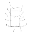
図1に示すように、ウェーハ11は裏面に粘着性の保持シート12が貼り付けられており、保持シート12は金属製のリング13に取付けられている。ウェーハ11はこのように保持シート12を介して金属製のリング13に取付けられた状態でハンドリングされる。そして、図2に示すように、ウェーハ11は切断工程で表面側からダイシングソーなどによって切断されて各半導体ダイ15となる。各半導体ダイ15の間にはダイシングの際に出来た切り込み隙間14が出来る。切り込み隙間14の深さは半導体ダイ15から保持シート12の一部にまで達しているが、保持シート12は切断されておらず、各半導体ダイ15は保持シート12によって保持されている。
As shown in FIG. 1, an adhesive holding sheet 12 is attached to the back surface of the wafer 11, and the holding sheet 12 is attached to a metal ring 13. The wafer 11 is handled in such a state that it is attached to the metal ring 13 via the holding sheet 12 in this way. As shown in FIG. 2, the wafer 11 is cut by a dicing saw or the like from the surface side into a semiconductor die 15 in the cutting process. A notch gap 14 formed during dicing is formed between the semiconductor dies 15. The depth of the cut gap 14 reaches from the semiconductor die 15 to a part of the holding sheet 12, but the holding sheet 12 is not cut and each semiconductor die 15 is held by the holding sheet 12.
このように、保持シート12とリング13とが取付けられた半導体ダイ15は図3に示すように、ウェーハホルダ10に取付けられる。ウェーハホルダ10は、フランジ部を持つ円環状のエキスパンドリング16とエキスパンドリング16のフランジの上にリング13を固定するリング押さえ17とを備えている。リング押さえ17は図示しないリング押さえ駆動部によってエキスパンドリング16のフランジに向かって進退する方向に駆動される。エキスパンドリング16の内径は半導体ダイ15が配置されているウェーハの径よりも大きく、エキスパンドリング16は所定の厚さを備えており、フランジはエキスパンドリング16の外側にあって、保持シート12から離れた方向の端面側に外側に突出するように取付けられている。また、エキスパンドリング16の保持シート12側の外周は保持シート12をエキスパンドリング16に取付ける際に、保持シート12をスムーズに引き伸ばすことができるように曲面構成となっている。また、ウェーハホルダ10は図示しないウェーハホルダ水平方向駆動部によって保持シート12の面に沿った方向に移動することができるように構成されている。
As described above, the semiconductor die 15 to which the holding sheet 12 and the ring 13 are attached is attached to the wafer holder 10 as shown in FIG. The wafer holder 10 includes an annular expand ring 16 having a flange portion and a ring presser 17 for fixing the ring 13 on the flange of the expand ring 16. The ring retainer 17 is driven in a direction to advance and retract toward the flange of the expand ring 16 by a ring retainer drive unit (not shown). The inner diameter of the expand ring 16 is larger than the diameter of the wafer on which the semiconductor die 15 is arranged, the expand ring 16 has a predetermined thickness, and the flange is outside the expand ring 16 and is separated from the holding sheet 12. It is attached so as to protrude outward on the end face side in the direction. Further, the outer periphery of the expanding ring 16 on the holding sheet 12 side has a curved surface configuration so that the holding sheet 12 can be smoothly stretched when the holding sheet 12 is attached to the expanding ring 16. Further, the wafer holder 10 is configured to be movable in a direction along the surface of the holding sheet 12 by a wafer holder horizontal direction drive unit (not shown).
図3(b)に示すように、半導体ダイ15が貼り付けられた保持シート12はエキスパンドリング16にセットされる前は略平面状態となっている。
As shown in FIG. 3B, the holding sheet 12 to which the semiconductor die 15 is attached is in a substantially planar state before being set on the expanding ring 16.
図4は半導体ダイのピックアップ装置100の構成を示す図であり、また図4は半導体ダイのピックアップ装置100に保持シート12に貼り付けられた半導体ダイ15をセットした状態を示している。この状態では、リング13の上にリング押さえ17が降下し、リング13をエキスパンドリング16のフランジとの間に挟み込んでいる。エキスパンドリング16の保持シート12の当たる上面とフランジ面との間には段差があるので、リング13がフランジ面に押し付けられると、保持シート12はエキスパンドリング16の上面とフランジ面との段差分だけエキスパンドリング16上部の曲面に沿って引き伸ばされる。このため、エキスパンドリング16の上に固定された保持シート12には保持シートの中心から周囲に向かう引っ張り力が働いている。また、この引っ張り力によって保持シート12が延びるので、保持シート12の上に貼り付けられた各半導体ダイ15間の隙間が広がっている。
FIG. 4 is a diagram showing a configuration of the semiconductor die pick-up apparatus 100, and FIG. 4 shows a state in which the semiconductor die 15 attached to the holding sheet 12 is set in the semiconductor die pick-up apparatus 100. In this state, the ring presser 17 is lowered on the ring 13, and the ring 13 is sandwiched between the flanges of the expand ring 16. Since there is a step between the upper surface where the holding sheet 12 of the expand ring 16 contacts and the flange surface, when the ring 13 is pressed against the flange surface, the holding sheet 12 is the same as the step between the upper surface of the expand ring 16 and the flange surface. The expansion ring 16 is stretched along the curved surface. For this reason, the holding sheet 12 fixed on the expand ring 16 is subjected to a pulling force from the center of the holding sheet toward the periphery. In addition, since the holding sheet 12 is extended by the pulling force, a gap between the semiconductor dies 15 attached on the holding sheet 12 is widened.
ウェーハホルダ10には保持シート12に沿った面でウェーハホルダ10を移動させるウェーハホルダ水平方向駆動部72が取付けられている。ウェーハホルダ水平方向駆動部72は、例えば、内部に設けたモータとギヤによってウェーハホルダ10を水平方向に駆動するものであってもよいし、外部に設けられたモータなどの駆動源によってガイドに沿ってXY方向にウェーハホルダ10を移動させるようなものであってもよい。また、ウェーハホルダ10の上部には半導体ダイ15を吸着移動させるコレット18が設けられている。コレット18は吸着面に半導体ダイ15を吸着するための吸着孔19を備え、各吸着孔19は真空装置71に接続されている。また、ウェーハホルダ10の下側にはステージ20が設けられ、ステージ20はステージ上下方向駆動機構73によって保持シート12に対して進退方向である上下方向に駆動される。ステージ上下方向駆動機構73は、例えば、内部に設けたモータとギヤによってステージ20を上下方向に駆動するものであってもよいし、外部に設けられたモータなどの駆動源によってガイドに沿って上下方向にステージ20を移動させるようなものであってもよい。
The wafer holder 10 is attached with a wafer holder horizontal direction driving unit 72 that moves the wafer holder 10 along a surface along the holding sheet 12. The wafer holder horizontal direction driving unit 72 may be, for example, a unit that drives the wafer holder 10 in the horizontal direction by a motor and a gear provided inside, or along a guide by a driving source such as a motor provided outside. The wafer holder 10 may be moved in the XY direction. In addition, a collet 18 for attracting and moving the semiconductor die 15 is provided on the wafer holder 10. The collet 18 includes suction holes 19 for sucking the semiconductor die 15 on the suction surface, and each suction hole 19 is connected to a vacuum device 71. In addition, a stage 20 is provided below the wafer holder 10, and the stage 20 is driven in a vertical direction that is an advancing / retreating direction with respect to the holding sheet 12 by a stage vertical direction driving mechanism 73. The stage vertical direction drive mechanism 73 may be, for example, a mechanism that drives the stage 20 in the vertical direction by a motor and a gear provided inside, or is vertically moved along a guide by a drive source such as a motor provided outside. The stage 20 may be moved in the direction.
図5に示すように、ステージ20はその上面に保持シート12に密着する密着面22を備えた円筒形の筐体21と、筐体21の密着面22と反対側に設けられた基体部24と、基体部24に取付けられ、筐体21の内部に取付けられたスライダ駆動機構300を駆動する駆動部25とを備えている。ステージ20の基体部24は図示しないステージ固定部に取付けられている。吸引開口41は、密着面22に設けられ、図4に示したピックアップする半導体ダイ15と略同一幅でその長さが半導体ダイ15よりも長く、ステージ20の内周側から外周側に向かって直線状に延びている。吸引開口41には、吸引開口41の幅と略同一幅で、吸引開口41の延びる方向に沿ってスライドして吸引開口41を開閉する蓋23が取り付けられている。蓋23はスライド方向に沿って吸引開口41を閉じる側が先端23aで、蓋23が開く側の端が後端23cである。蓋23の側面23bと吸引開口41の側面41bとはスライド面を構成している。吸引開口41は密着面22においてピックアップしようとする半導体ダイ15と略同一の幅となっていれば、内部に段差を設け、その段差部分にステージ20に連通するスリットを設けるように構成してあってもよい。
As shown in FIG. 5, the stage 20 has a cylindrical casing 21 having a close contact surface 22 in close contact with the holding sheet 12 on the upper surface thereof, and a base portion 24 provided on the opposite side of the close contact surface 22 of the casing 21. And a drive unit 25 that is attached to the base unit 24 and drives a slider drive mechanism 300 attached to the inside of the housing 21. The base portion 24 of the stage 20 is attached to a stage fixing portion (not shown). The suction opening 41 is provided in the contact surface 22, is substantially the same width as the semiconductor die 15 to be picked up shown in FIG. 4, and is longer than the semiconductor die 15, from the inner peripheral side of the stage 20 toward the outer peripheral side. It extends in a straight line. A lid 23 that slides along the direction in which the suction opening 41 extends and opens and closes the suction opening 41 is attached to the suction opening 41. The side of the lid 23 that closes the suction opening 41 along the sliding direction is the front end 23a, and the end on the side where the lid 23 opens is the rear end 23c. The side surface 23b of the lid 23 and the side surface 41b of the suction opening 41 constitute a slide surface. If the suction opening 41 has substantially the same width as the semiconductor die 15 to be picked up on the contact surface 22, a step is provided inside, and a slit communicating with the stage 20 is provided in the step portion. May be.
図6、図7に示すように、蓋23の先端23aは吸引開口41を閉じる際には吸引開口41のステージ内周側にある端面41aに押し当てられる。蓋23の先端23aは、吸引開口41を閉じる側に向かって凸の曲面であり、蓋23の先端23aが押し当てられる吸引開口の端面41aは、蓋23の先端23aの曲面に沿った曲面を備えている。曲面は円筒面でもよいし、複数の半径の円筒面を組み合わせたものでもよいし、他の形状の曲面で構成されていてもよい。
6 and 7, when the suction opening 41 is closed, the tip 23a of the lid 23 is pressed against the end surface 41a on the stage inner peripheral side of the suction opening 41. The tip 23 a of the lid 23 is a curved surface that is convex toward the side of closing the suction opening 41, and the end surface 41 a of the suction opening against which the tip 23 a of the lid 23 is pressed has a curved surface along the curved surface of the tip 23 a of the lid 23. I have. The curved surface may be a cylindrical surface, a combination of cylindrical surfaces having a plurality of radii, or a curved surface having another shape.
また、蓋23の先端23aが接する側の吸引開口41の両角部には、吸引開口41の側面41bから吸引開口41の幅方向に向かって突出し、密着面22からステージ20の内面に向かって上下方向に延びて保持シート12を吸引する縦溝364を有している。縦溝364は、吸引開口41とつながった略270度の扇型の円筒面によって構成され、吸引開口41の両角部において、各縦溝364の円筒面に接する接線500が端面41aの円筒面の接線となる位置まで蓋23が閉となる方向に向かって端面41aよりも突出している。
Further, the corners of the suction opening 41 on the side where the tip 23 a of the lid 23 contacts are projected from the side surface 41 b of the suction opening 41 toward the width direction of the suction opening 41, and vertically moved from the contact surface 22 toward the inner surface of the stage 20. A longitudinal groove 364 that extends in the direction and sucks the holding sheet 12 is provided. The vertical groove 364 is configured by a fan-shaped cylindrical surface of approximately 270 degrees connected to the suction opening 41, and the tangent line 500 that contacts the cylindrical surface of each vertical groove 364 at both corners of the suction opening 41 is the cylindrical surface of the end surface 41a. It protrudes from the end face 41a in the direction in which the lid 23 is closed to a position that becomes a tangent.
図7(a)に示すように、蓋23が閉じた場合には、蓋23の先端23aは端面41aに接するので、蓋23が閉じた状態では、蓋23、吸引開口41の両角部には、略270度の扇型の円筒面を持つ縦溝364が密着面22と筐体21の内部とを連通する。また、図7(b)に示すように、半導体ダイ15の一端15aを吸引開口41の端面41aあるいは蓋23の先端23aに合わせた場合には、半導体ダイ15の一部は、蓋23の先端23aからはみ出し、略90度の扇形の斜線部分は縦溝364の上に位置する。
As shown in FIG. 7A, when the lid 23 is closed, the tip 23a of the lid 23 contacts the end surface 41a. Therefore, when the lid 23 is closed, both corners of the lid 23 and the suction opening 41 are provided. A vertical groove 364 having a fan-shaped cylindrical surface of approximately 270 degrees communicates the contact surface 22 and the inside of the housing 21. 7B, when the one end 15a of the semiconductor die 15 is aligned with the end face 41a of the suction opening 41 or the tip 23a of the lid 23, a part of the semiconductor die 15 is part of the tip of the lid 23. The fan-shaped hatched portion that protrudes from 23 a and is approximately 90 degrees is located above the vertical groove 364.
図8に示すように、蓋23は吸引開口41を閉じた際には保持シート12側にある表面が密着面22と略同一面となる。蓋23の表面の周囲には面取り部分23eが設けられており、蓋23が吸引開口41を閉じた際には、密着面22と蓋23との間には小さなV字形の溝が形成される。また、先に説明したように、吸引開口41の幅と蓋23の幅と半導体ダイ15の幅はそれぞれ略同一で、吸引開口41の各側面41bと蓋23の各側面23bはスライドするように接している。
As shown in FIG. 8, when the lid 23 closes the suction opening 41, the surface on the holding sheet 12 side becomes substantially flush with the contact surface 22. A chamfered portion 23 e is provided around the surface of the lid 23, and when the lid 23 closes the suction opening 41, a small V-shaped groove is formed between the contact surface 22 and the lid 23. . Further, as described above, the width of the suction opening 41, the width of the lid 23, and the width of the semiconductor die 15 are substantially the same, and the side surfaces 41b of the suction opening 41 and the side surfaces 23b of the lid 23 slide. It touches.
図5に示すように、ステージ20は、密着面22から蓋23の厚さだけ凹み、蓋23と略同一幅で蓋23が開く側の吸引開口41の端からステージ20の外周側に向かって延びるスライド用溝22aと、スライド用溝22aの底面22a’に続く傾斜面22bとを備えている。スライド用溝22aの側面22hは吸引開口41の側面41bと同一の面となっており、蓋23の側面23bとスライド用溝22aの側面22hとはスライド面を構成している。スライド用溝22aの底面22a’は密着面22に略平行に、ステージ20外周の円筒面にかからない位置で、蓋23が吸引開口41を閉じた状態での蓋23の後端23cの位置よりもステージ内周側の位置にある端部22cまで延びている。端部22cは直線状で、蓋23の後端23cは蓋23が閉じた状態でスライド用溝22aの端部22cよりも若干ステージ20外周側に突出している。傾斜面22bは、スライド用溝22aの端部22cから密着面22と反対の方向の下側に向かって傾斜している。傾斜面22bの両側にはスライド用溝22aの側面22hと同一面となっている側面22jが延びている。側面22jと蓋23の側面23bとはスライド面を構成している。傾斜面22bとスライド用溝22aの底面22a’との交線は蓋23のスライド方向と直角方向に延びる直線状の稜線のエッジ22dを形成している。蓋23の後端23cは蓋23が吸引開口41を閉じた状態でスライド用溝22aの端部22c、及びエッジ22dよりもステージ20の外周側に突出しているので、蓋23の保持シート12を押し上げる面と反対側の面である下面23gはエッジ22dで支持される。
As shown in FIG. 5, the stage 20 is recessed from the contact surface 22 by the thickness of the lid 23, and is substantially the same width as the lid 23 from the end of the suction opening 41 on the side where the lid 23 opens to the outer peripheral side of the stage 20. An extending slide groove 22a and an inclined surface 22b following the bottom surface 22a 'of the slide groove 22a are provided. The side surface 22h of the slide groove 22a is the same surface as the side surface 41b of the suction opening 41, and the side surface 23b of the lid 23 and the side surface 22h of the slide groove 22a constitute a slide surface. The bottom surface 22 a ′ of the slide groove 22 a is substantially parallel to the contact surface 22 and does not cover the cylindrical surface of the outer periphery of the stage 20, and is more than the position of the rear end 23 c of the lid 23 when the lid 23 closes the suction opening 41. It extends to the end 22c located at the stage inner peripheral side. The end 22c is linear, and the rear end 23c of the lid 23 projects slightly toward the outer periphery of the stage 20 from the end 22c of the slide groove 22a with the lid 23 closed. The inclined surface 22b is inclined downward from the end 22c of the sliding groove 22a in the direction opposite to the contact surface 22. Side surfaces 22j that are flush with the side surface 22h of the sliding groove 22a extend on both sides of the inclined surface 22b. The side surface 22j and the side surface 23b of the lid 23 constitute a slide surface. A line of intersection between the inclined surface 22b and the bottom surface 22a 'of the slide groove 22a forms a linear ridge line edge 22d extending in a direction perpendicular to the slide direction of the lid 23. The rear end 23c of the lid 23 protrudes to the outer peripheral side of the stage 20 from the end 22c of the slide groove 22a and the edge 22d in a state where the lid 23 closes the suction opening 41. The lower surface 23g, which is the surface opposite to the surface to be pushed up, is supported by the edge 22d.
図4に示すように、本実施形態の半導体ダイのピックアップ装置100は、蓋23が回転自在に取り付けられたスライダ332をスライドさせるスライダ駆動機構300がステージ20の内部に設けられている。スライダ駆動機構300はステージ20の基体部24に取付けられた駆動部25によって密着面22に対して進退方向に駆動される第1リンク326と、ステージ20の筐体21に滑動自在に取付けられ、密着面22に対して進退するピストン370と、筐体21の内部に設けられ、ピストン370のフランジ371に係合してピストン370の密着面22に対する進退方向の動作を制限するストッパ321aと、第1リンク326とピストン370とを密着面22に対して進退する方向に接続するばね373と、ピストン370に取付けられ、密着面22に略平行で吸引開口41の延びる方向に延びるガイドレール331と、ガイドレール331に滑動自在に取付けられたスライダ332と、ピストン370にピン328によって回転自在に取付けられ、スライダ332と第1リンク326とを接続し、ピストン370がストッパ321aに当接すると、第1リンク326の密着面22に対する進退方向の動作をスライダ332のガイドレール331に沿った方向の動作に変換する第2リンク329と、によって構成されている。スライダ332には吸引開口41の幅方向に延びる円筒形状のピン330が取り付けられ、ピン330には、蓋23の先端23aから吸引開口41を閉じる側に張り出したアーム23fに設けられた逆U字型の切り欠きが回転自在に係合している。また、筐体21は真空装置71に接続され、内部を真空にすることができるよう構成されている。
As shown in FIG. 4, in the semiconductor die pick-up device 100 of this embodiment, a slider drive mechanism 300 for sliding a slider 332 to which a lid 23 is rotatably attached is provided inside the stage 20. The slider drive mechanism 300 is slidably attached to the first link 326 driven in the forward and backward direction with respect to the contact surface 22 by the drive unit 25 attached to the base portion 24 of the stage 20 and the housing 21 of the stage 20. A piston 370 that moves forward and backward with respect to the contact surface 22; a stopper 321a that is provided inside the housing 21 and that engages with a flange 371 of the piston 370 to limit the movement of the piston 370 in the forward / backward direction; A spring 373 that connects one link 326 and the piston 370 in a direction that advances and retreats with respect to the contact surface 22; a guide rail 331 that is attached to the piston 370 and extends substantially parallel to the contact surface 22 and extends in the direction of the suction opening 41; A slider 332 slidably attached to the guide rail 331 and a piston 370 can be freely rotated by a pin 328. When the slider 332 and the first link 326 are connected and the piston 370 contacts the stopper 321a, the movement of the first link 326 in the advancing / retreating direction with respect to the contact surface 22 is performed in the direction along the guide rail 331 of the slider 332. And a second link 329 for converting the operation. A cylindrical pin 330 extending in the width direction of the suction opening 41 is attached to the slider 332, and an inverted U-shape provided on an arm 23 f that protrudes from the tip 23 a of the lid 23 toward the closing side of the suction opening 41. The mold notch is rotatably engaged. Moreover, the housing | casing 21 is connected to the vacuum apparatus 71, and is comprised so that an inside can be made into a vacuum.
第2リンク329は一端に設けられたピン327が第1リンク326の係合溝326aに入り、他端に設けられた係合溝329aがスライダ332のピン330aを挟み込むことによってスライダ332と第1リンク326とを接続している。駆動部25の内部には、スライダ駆動機構300を動作させるためのモータ381が取付けられており、モータ381の回転軸には第1リンク326のシャフト326bの先端に設けられたローラ326cに接するカム383が取付けられている。
In the second link 329, the pin 327 provided at one end enters the engagement groove 326a of the first link 326, and the engagement groove 329a provided at the other end sandwiches the pin 330a of the slider 332, whereby the first link 326 and the first link 326 are engaged with the first link 326. A link 326 is connected. A motor 381 for operating the slider drive mechanism 300 is attached inside the drive unit 25, and a cam that contacts a roller 326 c provided at the tip of the shaft 326 b of the first link 326 on the rotating shaft of the motor 381. 383 is attached.
このように、スライダ駆動機構300は密着面22に向かって進退方向に動作する第1リンク326の動作をL字形の第2リンク329によってスライダ332を密着面22に平行に移動させる方向の動作に変換しているため、コンパクトな構成とすることができ、円筒形状の筐体21の内部にその機構を収納することができるようになっている。
As described above, the slider drive mechanism 300 changes the operation of the first link 326 that moves in the forward and backward direction toward the contact surface 22 to the operation in the direction in which the slider 332 is moved in parallel with the contact surface 22 by the L-shaped second link 329. Since it is converted, the structure can be made compact, and the mechanism can be stored inside the cylindrical casing 21.
図4に示すように、半導体ダイのピックアップ装置100は、CPUなどを内部に含むコンピュータである制御部70を備え、駆動部25、真空装置71、コレット18及びウェーハホルダ水平方向駆動部72、ステージ上下方向駆動機構73がそれぞれ接続され、駆動部25、真空装置71、コレット18及びウェーハホルダ水平方向駆動部72、ステージ上下方向駆動機構73は制御部70から出力される指令によって駆動されるよう構成されている。なお、図4において1点鎖線は制御部70と駆動部25、真空装置71、コレット18及びウェーハホルダ水平方向駆動部72、ステージ上下方向駆動機構73を接続する信号線を示している。
As shown in FIG. 4, a semiconductor die pick-up device 100 includes a control unit 70 which is a computer including a CPU and the like, and includes a driving unit 25, a vacuum device 71, a collet 18, a wafer holder horizontal driving unit 72, a stage. The vertical drive mechanism 73 is connected to each other, and the drive unit 25, vacuum device 71, collet 18 and wafer holder horizontal drive unit 72, and stage vertical drive mechanism 73 are configured to be driven by commands output from the control unit 70. Has been. In FIG. 4, a one-dot chain line indicates a signal line that connects the control unit 70, the drive unit 25, the vacuum device 71, the collet 18, the wafer holder horizontal direction drive unit 72, and the stage vertical direction drive mechanism 73.
次に、図9から図12を参照しながら半導体ダイのピックアップ装置100によって、保持シート12から半導体ダイ15をピックアップする動作について説明する。図1から図8を参照して説明した部分については同様の符号を付して説明は省略する。
Next, the operation of picking up the semiconductor die 15 from the holding sheet 12 by the semiconductor die pickup device 100 will be described with reference to FIGS. The portions described with reference to FIGS. 1 to 8 are denoted by the same reference numerals, and description thereof is omitted.
図9(a)に示すように、制御部70は蓋23が閉じた状態で蓋23と半導体ダイ15との位置合わせ工程を開始する。蓋23は吸引開口41を閉じた位置にあるので、蓋23の先端23aは吸引開口41の端面41aに接した位置となっており、蓋23の後端23cの下面はスライド用溝22aの表面に載って、スライド用溝22aによって支持されている。また、蓋23の表面と密着面22とは略同一面となっている。制御部70は、図4に示したウェーハホルダ水平方向駆動部72によってウェーハホルダ10をステージ20の待機位置の上まで水平方向に移動させる。そして、制御部70は、ウェーハホルダ10がステージ20の待機位置の上の所定の位置まで移動したら、ウェーハホルダ10の水平方向の移動を一端停止し、ステージ上下方向駆動機構73によってステージ20の密着面22と蓋23の表面が保持シート12の下面に密着するまでステージ20を上昇させる。ステージ20の密着面22と蓋23の表面が保持シート12の下面に密着したら、制御部70はステージ20の上昇を停止する。そして、制御部70は、再度ウェーハホルダ水平方向駆動部72によって、閉じている状態の蓋23の先端23aにピックアップする半導体ダイ15の一端15aを合わせ、蓋23の幅方向位置と半導体ダイ15の幅方向位置とを合わせ、半導体ダイ15の側面が蓋23の側面23bに合うように調整する。蓋23の幅はピックアップしようとする半導体ダイ15と略同一幅であるので、一方の側面23bを半導体ダイ15の側面にあわせると、半導体ダイ15の各側面と蓋23の各側面23bとの位置合わせを行うことができる。この時、保持シート12はウェーハホルダ10のエキスパンドリング16によって引っ張り力を受けている。
As shown in FIG. 9A, the control unit 70 starts the alignment process between the lid 23 and the semiconductor die 15 with the lid 23 closed. Since the lid 23 is in a position where the suction opening 41 is closed, the tip 23a of the lid 23 is in contact with the end surface 41a of the suction opening 41, and the lower surface of the rear end 23c of the lid 23 is the surface of the slide groove 22a. And is supported by the slide groove 22a. Further, the surface of the lid 23 and the contact surface 22 are substantially the same surface. The controller 70 moves the wafer holder 10 horizontally above the standby position of the stage 20 by the wafer holder horizontal direction driving unit 72 shown in FIG. Then, when the wafer holder 10 moves to a predetermined position above the standby position of the stage 20, the controller 70 once stops the horizontal movement of the wafer holder 10, and the stage 20 is brought into close contact with the stage vertical drive mechanism 73. The stage 20 is raised until the surface 22 and the surface of the lid 23 are in close contact with the lower surface of the holding sheet 12. When the contact surface 22 of the stage 20 and the surface of the lid 23 are in close contact with the lower surface of the holding sheet 12, the control unit 70 stops raising the stage 20. Then, the control unit 70 again aligns the one end 15a of the semiconductor die 15 to be picked up with the tip 23a of the lid 23 in the closed state by the wafer holder horizontal direction driving unit 72, and the position in the width direction of the lid 23 and the position of the semiconductor die 15 The width direction position is adjusted and adjusted so that the side surface of the semiconductor die 15 matches the side surface 23 b of the lid 23. Since the width of the lid 23 is substantially the same as that of the semiconductor die 15 to be picked up, the position of each side surface of the semiconductor die 15 and each side surface 23b of the lid 23 when the one side surface 23b is aligned with the side surface of the semiconductor die 15. Can be combined. At this time, the holding sheet 12 receives a tensile force by the expanding ring 16 of the wafer holder 10.
図9(b)はステージ20の密着面22と蓋23の表面の平面図であり、その上に載っている保持シート12と半導体ダイ15を1点鎖線で表示してその位置関係がわかるようにした図で、図9(b)では略同一幅の半導体ダイ15と蓋23とを区別するために蓋23を半導体ダイ15よりも若干大きく図示している。図10(b)、図12(b)も同様である。図9(b)に示すように、蓋23と半導体ダイ15との位置が合わせられると、半導体ダイ15の略90度の扇形の斜線部分は縦溝364の上に位置する。
FIG. 9B is a plan view of the contact surface 22 of the stage 20 and the surface of the lid 23. The holding sheet 12 and the semiconductor die 15 placed thereon are indicated by a one-dot chain line so that the positional relationship can be understood. In FIG. 9B, the lid 23 is shown slightly larger than the semiconductor die 15 in order to distinguish between the semiconductor die 15 and the lid 23 having substantially the same width. The same applies to FIGS. 10B and 12B. As shown in FIG. 9 (b), when the positions of the lid 23 and the semiconductor die 15 are aligned, the approximately 90-degree fan-shaped hatched portion of the semiconductor die 15 is located on the vertical groove 364.
ステージ20の保持シート12の下面への進出、密着と半導体ダイ15の位置合わせとが終わると、制御部70は位置合わせ工程を終了する。そして、制御部70は、コレット18をピックアップしようとする半導体ダイ15の直上に移動し、半導体ダイ15と若干の隙間を開けた高さに保持する。制御部70はコレット18の移動が終わると真空装置71によって吸着孔19から空気の吸引を開始し、コレット18を半導体ダイ15の吸着待機状態とする。
When the advancement and adhesion of the stage 20 to the lower surface of the holding sheet 12 and the alignment of the semiconductor die 15 are completed, the control unit 70 ends the alignment process. Then, the control unit 70 moves to the position immediately above the semiconductor die 15 from which the collet 18 is to be picked up, and holds the collet 18 at a height with a slight gap. When the movement of the collet 18 is finished, the control unit 70 starts sucking air from the suction hole 19 by the vacuum device 71, and puts the collet 18 in a suction standby state of the semiconductor die 15.
図10から図13に示すように、制御部70は保持シート引き剥がし工程を開始する。制御部70は真空装置71によってステージ20の筐体21の内部を真空とする。筐体21の内部の圧力を真空にすると、図10(b)に示す筐体21の内部と連通している縦溝364も真空となり、保持シート12を密着面22に吸着する。この際、保持シート12は、真空によって下向きに引かれるがこの状態ではまだ保持シート12は半導体ダイ15から剥離していない。また、図8に示した蓋23の表面に設けられた面取り部分23eと吸引開口41との間のV字形の溝には、ステージ20の外周側から真空となる縦溝364に向かって空気が流れている。このV字形の溝の圧力は大気圧よりは低い圧力であるが、この負圧では保持シート12は剥がれていない。
10 to 13, the control unit 70 starts the holding sheet peeling process. The control unit 70 evacuates the inside of the casing 21 of the stage 20 using the vacuum device 71. When the pressure inside the housing 21 is evacuated, the vertical groove 364 communicating with the inside of the housing 21 shown in FIG. 10B is also evacuated, and the holding sheet 12 is attracted to the contact surface 22. At this time, the holding sheet 12 is pulled downward by the vacuum, but in this state, the holding sheet 12 is not yet peeled from the semiconductor die 15. Further, in the V-shaped groove between the chamfered portion 23e provided on the surface of the lid 23 shown in FIG. 8 and the suction opening 41, air flows from the outer peripheral side of the stage 20 toward the vertical groove 364 that becomes a vacuum. Flowing. The pressure in the V-shaped groove is lower than the atmospheric pressure, but the holding sheet 12 is not peeled off at this negative pressure.
図10(a)に示すように、制御部70の指令によってスライダ駆動機構300の駆動部25のモータ381が回転すると、モータ381の軸に取付けられているカム383が回転する。カム383は楕円形状で、カム面が第1リンク326のシャフト326bの先端に取付けられたローラ326cに接しており、図10(a)の矢印の方向に回転するとカム383のカム面はローラ326cを密着面22の方向に向かって押し上げる。この動作によってシャフト326bが上昇し、第1リンク326全体が密着面22に向かって上昇する。第1リンク326全体が上昇すると、密着面22の側にばね373によって接続されているピストン370は第1リンク326によって押し上げられて、ピストン370の全体が密着面22に向かって上昇する。ピストン370の全体が密着面22に向かって上昇すると、密着面22の側に取付けられているガイドレール331もピストン370とともに密着面22に向かって上昇する。ガイドレール331が上昇すると、ガイドレール331の上面に沿ってスライドするよう取付けられているスライダ332も密着面22に向かって上昇する。そして、スライダ332にアーム23fを介して回転自在に係合されている蓋23の先端23aは、スライダ332の上昇と共に密着面22から上方に向かって進出する。
As shown in FIG. 10A, when the motor 381 of the drive unit 25 of the slider drive mechanism 300 is rotated by a command from the control unit 70, the cam 383 attached to the shaft of the motor 381 is rotated. The cam 383 has an elliptical shape, and the cam surface is in contact with the roller 326c attached to the tip of the shaft 326b of the first link 326. When the cam 383 rotates in the direction of the arrow in FIG. 10A, the cam surface of the cam 383 becomes the roller 326c. Is pushed up toward the contact surface 22. By this operation, the shaft 326 b rises and the entire first link 326 rises toward the contact surface 22. When the entire first link 326 rises, the piston 370 connected to the contact surface 22 side by the spring 373 is pushed up by the first link 326, and the entire piston 370 rises toward the contact surface 22. When the entire piston 370 rises toward the contact surface 22, the guide rail 331 attached to the contact surface 22 side also moves up toward the contact surface 22 together with the piston 370. When the guide rail 331 rises, the slider 332 attached so as to slide along the upper surface of the guide rail 331 also rises toward the contact surface 22. The tip 23a of the lid 23 that is rotatably engaged with the slider 332 via the arm 23f advances upward from the contact surface 22 as the slider 332 rises.
蓋23の先端23aが密着面22から上方に向かって進出すると蓋23の先端23aは、保持シート12と半導体ダイ15の一端15aを押し上げる。すると、先端23aは保持シート12から下向きの力を受けるので、蓋23はピン330を中心に時計方向に回転する。蓋23の保持シート12を押し上げる面と反対側の面である下面23gは、スライド用溝22aと傾斜面22bとの間のエッジ22dで支持され、後端23cの保持シート12側の面は密着面22と略同一面になっているので、蓋23の保持シート12を押し上げている表面は蓋23の先端23a側から後端23c側に向かって下向きに傾斜する。傾斜角度は、密着面22に対して角度αである。一方、傾斜面22bは密着面22に対して角度αよりも大きい角度βだけ傾斜している。このため、傾斜面22bは蓋23の後端23cの移動を妨げることが無く、蓋23の下面23gは常にエッジ22dと線接触する。
When the tip 23 a of the lid 23 advances upward from the contact surface 22, the tip 23 a of the lid 23 pushes up the holding sheet 12 and one end 15 a of the semiconductor die 15. Then, since the tip 23 a receives a downward force from the holding sheet 12, the lid 23 rotates clockwise about the pin 330. The lower surface 23g, which is the surface opposite to the surface that pushes up the holding sheet 12 of the lid 23, is supported by an edge 22d between the slide groove 22a and the inclined surface 22b, and the surface of the rear end 23c on the holding sheet 12 side is in close contact. Since the surface is substantially flush with the surface 22, the surface of the lid 23 that pushes up the holding sheet 12 is inclined downward from the front end 23a side of the lid 23 toward the rear end 23c side. The inclination angle is an angle α with respect to the contact surface 22. On the other hand, the inclined surface 22b is inclined with respect to the contact surface 22 by an angle β larger than the angle α. For this reason, the inclined surface 22b does not hinder the movement of the rear end 23c of the lid 23, and the lower surface 23g of the lid 23 is always in line contact with the edge 22d.
蓋23の先端23aが上昇するにつれて、蓋23はピックアップしようとする半導体ダイ15と保持シート12とを上に押し上げる。一方、真空となった縦溝364の上に位置している半導体ダイ15の両角の部分の保持シート12は密着面22に吸引固定されている。このため、蓋23の上昇によって、ピックアップしようとする半導体ダイ15に張りつけられている保持シート12は密着面22に向かって斜め下向きに引っ張られ、この斜め下向きの引っ張り力によって縦溝364の上に位置している半導体ダイ15の両角の部分から保持シート12が剥がれ始め、縦溝364の上に位置している略90度の扇形部分の保持シート12が剥がれる。そして、蓋23の先端23aが上昇するにつれて蓋23の先端23aよりも密着面22にはみ出している半導体ダイ15の略三角形状の部分の保持シート12が密着面22に向かって斜め下向きに引っ張られ、半導体ダイ15の幅方向の両側から幅方向の中心に向かって剥がれていく。
As the tip 23a of the lid 23 rises, the lid 23 pushes up the semiconductor die 15 and the holding sheet 12 to be picked up. On the other hand, the holding sheets 12 at both corners of the semiconductor die 15 located on the vertical grooves 364 that have become vacuum are sucked and fixed to the contact surface 22. For this reason, when the lid 23 is raised, the holding sheet 12 attached to the semiconductor die 15 to be picked up is pulled obliquely downward toward the contact surface 22, and the diagonal downward pulling force causes the holding sheet 12 to be placed on the vertical groove 364. The holding sheet 12 begins to peel from both corners of the semiconductor die 15 positioned, and the approximately 90-degree fan-shaped holding sheet 12 positioned on the longitudinal groove 364 is peeled off. Then, as the tip 23 a of the lid 23 rises, the holding sheet 12 of the substantially triangular portion of the semiconductor die 15 that protrudes from the tip 23 a of the lid 23 to the contact surface 22 is pulled obliquely downward toward the contact surface 22. The semiconductor die 15 is peeled from both sides in the width direction toward the center in the width direction.
そして、制御部70の指令によって更にスライダ駆動機構300のモータ381が回転し、モータ381と共に回転するカム383によって更に第1リンク326とピストン370とが密着面22の方向に向かって上昇すると、ピストン370の外面に張り出したフランジ371の端面が筐体21に設けられたストッパ321aにぶつかる。するとピストン370はストッパ321aによって密着面22に対してそれ以上進出できなくなり、蓋23の先端23aの密着面22からの進出が所定の位置で停止する。先端23aが所定の位置まで上昇すると、先端23aの曲面に沿って保持シート12の剥離線53が形成される。
When the motor 381 of the slider drive mechanism 300 further rotates according to the command from the control unit 70, and the first link 326 and the piston 370 further rise in the direction of the contact surface 22 by the cam 383 that rotates together with the motor 381, the piston The end surface of the flange 371 projecting to the outer surface of 370 hits the stopper 321 a provided on the housing 21. Then, the piston 370 can no longer advance with respect to the contact surface 22 by the stopper 321a, and the advancement of the tip 23a of the lid 23 from the contact surface 22 stops at a predetermined position. When the tip 23a rises to a predetermined position, a peeling line 53 of the holding sheet 12 is formed along the curved surface of the tip 23a.
図11に示すように、蓋23の先端23aが上昇するにつれて蓋23が回転するので、蓋23の先端23aは半導体ダイ15の一端15aよりも蓋23のスライド方向に向かってわずかに移動する。このため、剥離線53は半導体ダイ15の一端15aよりもわずかに蓋23のスライド方向に寄った位置に形成される。
As shown in FIG. 11, since the lid 23 rotates as the tip 23a of the lid 23 rises, the tip 23a of the lid 23 moves slightly toward the sliding direction of the lid 23 from one end 15a of the semiconductor die 15. For this reason, the peeling line 53 is formed at a position slightly closer to the sliding direction of the lid 23 than the one end 15 a of the semiconductor die 15.
図11に示すように、半導体ダイ15の保持シート12が剥がれた部分は、保持シート12によって密着面22に向かって引かれる力がなくなる。また、保持シート12が剥がれた一端15aから剥離線53までの部分の半導体ダイ15と保持シート12との間には空気が入り込み、この部分の半導体ダイ15の保持シート12側の面の圧力は大気圧となる。一方、半導体ダイ15のコレット18側の面は、蓋23の先端23aの上方への進出によってコレット18の吸着面に接近することにより圧力が低下する。このため、半導体ダイ15の保持シート12側の面の圧力がコレット18側の圧力よりも高くなり、保持シート12から剥がれた半導体ダイ15の部分はコレット18に吸着される。半導体ダイ15の剥離線53から蓋23の後端23c側にあってまだ保持シート12が剥がれていない部分は、半導体ダイ15とコレット18との間に若干の隙間が残っており、半導体ダイ15の保持シート12側とコレット18側との圧力差があまり大きくなっていないことと、保持シート12による引き下げ力があることにより、まだコレット18に吸着されていない。このため、半導体ダイ15は、コレット18に吸着された部分とコレット18に吸着されていない部分との間で微小な曲げ変形を生じている。
As shown in FIG. 11, the portion of the semiconductor die 15 from which the holding sheet 12 is peeled loses the force drawn toward the contact surface 22 by the holding sheet 12. In addition, air enters between the portion of the semiconductor die 15 from the one end 15a where the holding sheet 12 is peeled off to the peeling line 53 and the holding sheet 12, and the pressure on the surface of the semiconductor die 15 on the holding sheet 12 side of this portion is It becomes atmospheric pressure. On the other hand, the pressure on the surface of the semiconductor die 15 on the collet 18 side is reduced by approaching the adsorption surface of the collet 18 by the upward movement of the tip 23a of the lid 23. For this reason, the pressure of the surface of the semiconductor die 15 on the holding sheet 12 side becomes higher than the pressure on the collet 18 side, and the portion of the semiconductor die 15 peeled off from the holding sheet 12 is adsorbed by the collet 18. A portion of the semiconductor die 15 on the rear end 23c side of the lid 23 from the peeling line 53 where the holding sheet 12 has not yet been peeled is left with a slight gap between the semiconductor die 15 and the collet 18. Since the pressure difference between the holding sheet 12 side and the collet 18 side is not so large and there is a pulling force by the holding sheet 12, it is not yet adsorbed by the collet 18. For this reason, the semiconductor die 15 undergoes minute bending deformation between a portion adsorbed by the collet 18 and a portion not adsorbed by the collet 18.
図10(a)に示すように、蓋23の先端23aが密着面22から上方に進出し、保持シート12を押し上げている側の表面が傾斜すると、剥離線53よりも蓋23の後端23c側にある蓋23の表面と保持シート12との間には隙間が生じ、剥離線53よりも蓋23の後端23c側にある蓋23の表面の圧力は略大気圧となる。また、蓋23の面取り部分23eの表面の圧力は蓋23の表面の圧力と同様の大気圧となるため、先端23aに隣接する一部を除いて面取り部分23eの保持シート12は半導体ダイ15から剥がれていない。したがって、剥離線53は図10(b)に示すように、蓋23の先端23aに沿って半導体ダイ15の幅方向の側面から側面にかけて延びる線であり、蓋23の側面23bに沿った部分には剥離線53は延びていない。
As shown in FIG. 10A, when the front end 23 a of the lid 23 advances upward from the contact surface 22 and the surface on the side where the holding sheet 12 is pushed up is inclined, the rear end 23 c of the lid 23 with respect to the peeling line 53. A gap is generated between the surface of the lid 23 on the side and the holding sheet 12, and the pressure on the surface of the lid 23 on the rear end 23 c side of the lid 23 with respect to the peeling line 53 is substantially atmospheric pressure. Further, since the pressure on the surface of the chamfered portion 23e of the lid 23 is the same atmospheric pressure as the pressure on the surface of the lid 23, the holding sheet 12 of the chamfered portion 23e is removed from the semiconductor die 15 except for a portion adjacent to the tip 23a. Not peeled off. Therefore, as shown in FIG. 10B, the peeling line 53 is a line extending from the side surface in the width direction of the semiconductor die 15 to the side surface along the tip 23 a of the lid 23, and in the portion along the side surface 23 b of the lid 23. The peeling line 53 does not extend.
図10(a)に示すように、蓋23の厚さは、先端23aの密着面22からの所定の進出高さよりも厚いので、蓋23の各側面23bは吸引開口41の各側面41bと接した状態となっている。また、蓋23の後端23cの下面は、スライド用溝22aの表面に接している。そして、縦溝364の上には半導体ダイ15から剥がれた保持シート12が覆いかぶさっている。このため、筐体21の外部から筐体21の内部に向かってほとんど空気が流れこまないため筐体21の内部は真空に保持されている。
As shown in FIG. 10A, since the thickness of the lid 23 is thicker than a predetermined advance height from the contact surface 22 of the tip 23a, each side surface 23b of the lid 23 is in contact with each side surface 41b of the suction opening 41. It has become a state. The lower surface of the rear end 23c of the lid 23 is in contact with the surface of the slide groove 22a. The holding sheet 12 peeled off from the semiconductor die 15 is covered on the vertical groove 364. For this reason, since almost no air flows from the outside of the housing 21 toward the inside of the housing 21, the inside of the housing 21 is kept in a vacuum.
また、スライダ駆動機構300のばね373は蓋23の先端23aを密着面22から押し上げる程度ではほとんど撓まない程度のこわさを持っているので、蓋23の先端23aが密着面22から所定の進出高さまで押し上げられてもピストン370と第1リンク326との間の距離はほとんど変化しない。このため、第1リンク326の上昇によって蓋23は密着面22から突出するのみで、スライドはしていない。
Further, since the spring 373 of the slider drive mechanism 300 has such a stiffness that it hardly bends when the tip 23 a of the lid 23 is pushed up from the contact surface 22, the tip 23 a of the lid 23 has a predetermined advance height from the contact surface 22. Even if pushed up, the distance between the piston 370 and the first link 326 hardly changes. For this reason, the lid 23 only protrudes from the contact surface 22 by the rising of the first link 326 and does not slide.
図12(a)に示すように、制御部70の指令によって更にスライダ駆動機構300のカム383が回転し、第1リンク326が密着面22に向かって押し上げられると、密着面22に向かって移動できないピストン370と第1リンク326との間のばね373がモータ381とカム383によって密着面22に対して進退する方向に圧縮され始める。ばね373が圧縮されると、ピストン370は密着面22に対して進出せず、第1リンク326だけが密着面22に対して進出することとなる。このため、ピストン370のピン328は密着面22に対して上昇せず、第1リンク326の係合溝326aに入っている第2リンク329のピン327だけが密着面22の方向に上昇する。すると第2リンク329はピン328を中心に回転を始める。この回転動作によって第2リンク329の他端の係合溝329aがステージ20の外周側に向かって移動し、係合溝329aに入っているピン330aが固定されているスライダ332とスライダ332のピン330にアーム23fを介して回転自在に係合されている蓋23がステージ20の外周側に向かってスライドを始める。
As shown in FIG. 12A, when the cam 383 of the slider drive mechanism 300 is further rotated by a command from the control unit 70 and the first link 326 is pushed up toward the contact surface 22, it moves toward the contact surface 22. The spring 373 between the impossible piston 370 and the first link 326 starts to be compressed by the motor 381 and the cam 383 in the direction of moving back and forth with respect to the contact surface 22. When the spring 373 is compressed, the piston 370 does not advance with respect to the contact surface 22, and only the first link 326 extends with respect to the contact surface 22. For this reason, the pin 328 of the piston 370 does not rise with respect to the contact surface 22, and only the pin 327 of the second link 329 entering the engagement groove 326 a of the first link 326 rises in the direction of the contact surface 22. Then, the second link 329 starts to rotate around the pin 328. By this rotation operation, the engaging groove 329a at the other end of the second link 329 moves toward the outer periphery of the stage 20, and the slider 332 and the pin of the slider 332 to which the pin 330a in the engaging groove 329a is fixed. The lid 23 that is rotatably engaged with the 330 via the arm 23 f starts to slide toward the outer peripheral side of the stage 20.
図12(a)、図13に示すように、蓋23がスライドを始めると、蓋23の保持シート12を押し上げている表面と反対側の下面23gは、エッジ22dに接してエッジ22dに支持されながらスライドするので、蓋23の傾斜角度は蓋23がスライドするにつれて次第に大きくなってくる。しかし、蓋23がスライドした状態でも傾斜面22bと密着面22とのなす角度βは、蓋23と密着面22とのなす角度αよりも大きいので、蓋23の下面23gは傾斜面22bと干渉しない。そして、蓋23がスライドしている間、蓋23の下面23gは常にエッジ22dに接した状態となっている。
As shown in FIGS. 12A and 13, when the lid 23 starts to slide, the lower surface 23g of the lid 23 opposite to the surface pushing up the holding sheet 12 is in contact with the edge 22d and supported by the edge 22d. Therefore, the inclination angle of the lid 23 gradually increases as the lid 23 slides. However, since the angle β formed between the inclined surface 22b and the contact surface 22 is larger than the angle α formed between the cover 23 and the contact surface 22 even when the cover 23 is slid, the lower surface 23g of the cover 23 interferes with the inclined surface 22b. do not do. While the lid 23 is sliding, the lower surface 23g of the lid 23 is always in contact with the edge 22d.
図12(b)に示すように、蓋23がスライドすると、蓋23の先端23aが吸引開口41の端面41aから離れ、吸引開口41が開いてピックアップしようとする半導体ダイ15と略同一幅の開口開き部42ができる。ステージ20の筐体21の内部は真空装置71によって真空状態となっていることから、開口開き部42はその中に保持シート12を吸引する。そして、蓋23のスライドに伴って開口開き部42の中に保持シート12が引き込まれて半導体ダイ15から引き剥がされる。半導体ダイ15と保持シート12との間の剥離線53は蓋23の先端23aの曲面に沿った形状となるので、密着面22から蓋23の幅方向の中央が山形に盛り上がった稜線で、密着面22に沿った面内では蓋23の各側面23bの側は中央部分よりもスライド方向に向かって傾斜した線となっている。このため、半導体ダイ15の各側面側の保持シート12は半導体ダイ15の幅方向の中央部分の保持シート12よりも先に剥がれることとなる。このように、剥離線53が密着面22に沿った面内では半導体ダイ15の各端15a,15bに対してあるいはスライド方向に対して傾斜しているので、コレット18に吸着された部分とコレット18に吸着されていない部分との間の微小な曲げ変形によって発生する応力が緩和され、半導体ダイ15の損傷を効果的に抑制することができる。
As shown in FIG. 12B, when the lid 23 is slid, the tip 23a of the lid 23 is separated from the end face 41a of the suction opening 41, and the suction opening 41 is opened to have an opening having substantially the same width as the semiconductor die 15 to be picked up. An opening 42 is formed. Since the inside of the housing 21 of the stage 20 is in a vacuum state by the vacuum device 71, the opening opening 42 sucks the holding sheet 12 therein. Then, the holding sheet 12 is drawn into the opening portion 42 as the lid 23 slides, and is peeled off from the semiconductor die 15. Since the peeling line 53 between the semiconductor die 15 and the holding sheet 12 has a shape along the curved surface of the tip 23a of the lid 23, the center in the width direction of the lid 23 from the adhesion surface 22 is a ridge line that rises in a mountain shape. Within the surface along the surface 22, each side surface 23 b side of the lid 23 is a line inclined toward the sliding direction from the center portion. For this reason, the holding sheet 12 on each side of the semiconductor die 15 is peeled off before the holding sheet 12 at the center portion in the width direction of the semiconductor die 15. Thus, since the peeling line 53 is inclined with respect to the ends 15a and 15b of the semiconductor die 15 or with respect to the sliding direction in the plane along the contact surface 22, the portion adsorbed by the collet 18 and the collet The stress generated by a minute bending deformation between the portion not adsorbed by 18 is relieved, and damage to the semiconductor die 15 can be effectively suppressed.
蓋23のスライドにつれて開口開き部42はステージ20の外周側に向かって大きくなり、剥離線53も順次ステージ20の外周側に平行移動する。保持シート12は剥離線53に沿って半導体ダイ15の一端15aから他端15bに向かって順次剥がれ、開口開き部42に順次吸引される。
As the lid 23 slides, the opening portion 42 increases toward the outer peripheral side of the stage 20, and the peeling line 53 sequentially moves in parallel to the outer peripheral side of the stage 20. The holding sheet 12 is sequentially peeled from the one end 15 a to the other end 15 b of the semiconductor die 15 along the peeling line 53, and is sequentially sucked into the opening opening 42.
図13に示すように、蓋23がスライドして剥離線53が半導体ダイ15の一端15aから他端15bに向かって移動すると、図11を参照して説明したのと同様に、保持シート12が剥がれた一端15aから剥離線53までの部分の半導体ダイ15と保持シート12との間には空気が入り込み、この部分の半導体ダイ15の保持シート12側の面の圧力は大気圧となる。一方、半導体ダイ15のコレット18側の面は、コレット18の吸着面に接近することにより圧力が低下するので、保持シート12が剥がれた一端15aから剥離線53の手前までの半導体ダイ15の部分はコレット18に吸着される。そして、蓋23のスライドによって剥離線53が半導体ダイ15の一端15aから他端15bに向かって移動するにつれて、半導体ダイ15は一端15aから他端15bに向かって順次コレット18に吸着されていく。
As shown in FIG. 13, when the lid 23 slides and the peeling line 53 moves from one end 15 a of the semiconductor die 15 toward the other end 15 b, the holding sheet 12 is moved as described with reference to FIG. 11. Air enters between the part of the semiconductor die 15 and the holding sheet 12 from the peeled end 15a to the peeling line 53, and the pressure on the surface of the semiconductor die 15 on the side of the holding sheet 12 becomes atmospheric pressure. On the other hand, since the pressure of the surface of the semiconductor die 15 on the collet 18 side approaches the adsorption surface of the collet 18, the portion of the semiconductor die 15 from one end 15 a where the holding sheet 12 is peeled to the front of the peeling line 53. Is adsorbed by the collet 18. Then, as the peeling line 53 moves from one end 15a to the other end 15b of the semiconductor die 15 by the slide of the lid 23, the semiconductor die 15 is sequentially attracted to the collet 18 from the one end 15a to the other end 15b.
図12(a)、図13に示すように、蓋23がスライドすると、蓋23の保持シート12を押し上げている表面と反対側の下面23gがエッジ22dに接してスライドするので、エッジ22dと蓋23の下面23gの接線は大気圧の筐体21の外部と真空状態の筐体21の内部とを仕切るシール線となる。また、図5に示すように蓋23の側面23bとスライド用溝22aの側面22j及び蓋23と傾斜面22bの両側の側面22hはそれぞれスライド面を構成している。このため、蓋23の下面23gとスライド用溝22aの底面22a’との隙間および蓋23の側面23bと各側面22h,22jとの隙間から空気が筐体21の内部に入り込むことを抑制できるので、蓋23をスライドさせている間、筐体21の内部の真空を良好に保持でき、保持シート12を効果的に吸引開口41の中に真空吸引することができる。また、蓋23がスライドすると蓋23の後端23cは密着面22から下方に移動していくので、蓋23をスライドさせた際に蓋23の後端23cが隣接する半導体ダイ15にぶつかることが無く、蓋23のスライドによって隣接する半導体ダイ15を損傷させることが無いので、周囲に隣接した半導体ダイ15がある場合でも容易に半導体ダイ15をピックアップすることができる。
As shown in FIG. 12A and FIG. 13, when the lid 23 slides, the lower surface 23g opposite to the surface pushing up the holding sheet 12 of the lid 23 slides in contact with the edge 22d. The tangent line of the lower surface 23g of 23 is a seal line that separates the outside of the casing 21 at atmospheric pressure from the inside of the casing 21 in a vacuum state. Further, as shown in FIG. 5, the side surface 23b of the lid 23, the side surface 22j of the slide groove 22a, and the side surfaces 22h on both sides of the lid 23 and the inclined surface 22b constitute a slide surface. For this reason, air can be prevented from entering the inside of the casing 21 from the gap between the lower surface 23g of the lid 23 and the bottom surface 22a ′ of the sliding groove 22a and the gap between the side surface 23b of the lid 23 and the side surfaces 22h and 22j. While the lid 23 is being slid, the vacuum inside the casing 21 can be held well, and the holding sheet 12 can be effectively vacuumed into the suction opening 41. Further, when the lid 23 slides, the rear end 23c of the lid 23 moves downward from the contact surface 22, so that the rear end 23c of the lid 23 may hit the adjacent semiconductor die 15 when the lid 23 is slid. In addition, since the adjacent semiconductor die 15 is not damaged by the slide of the lid 23, the semiconductor die 15 can be easily picked up even when there are adjacent semiconductor dies 15.
また、引き剥がされた保持シート12によって開口開き部42が覆われるが、保持シート12を開口開き部42の中に吸引して、蓋23の先端23aが保持シート12の剥がれていない部分に向かってスライドしているので、開口開き部42による保持シート12の吸引が停止することが無く、保持シート12の全体を半導体ダイ15の一端15aから他端15bに向かって順次開口開き部42に吸引して引き剥がしていくことができ、引き剥がし残り部分ができないようにすることができる。
Further, the opening portion 42 is covered by the peeled holding sheet 12, but the holding sheet 12 is sucked into the opening portion 42, and the tip 23 a of the lid 23 faces the portion where the holding sheet 12 is not peeled off. Therefore, the suction of the holding sheet 12 by the opening 42 is not stopped, and the entire holding sheet 12 is sequentially sucked from the one end 15a of the semiconductor die 15 to the other end 15b by the opening 42. It can be peeled off and the remaining part of the peeling can be prevented.
半導体ダイ15に貼り付けられている保持シート12が全て剥がれると半導体ダイ15は全面的にコレット18に吸着され、コレット18によってピックアップされる。
When the holding sheet 12 attached to the semiconductor die 15 is completely peeled off, the semiconductor die 15 is entirely adsorbed by the collet 18 and picked up by the collet 18.
半導体ダイ15をピックアップした後、制御部70の指令によって更にスライダ駆動機構300のカム383が回転すると、今度はカム383の回転によって第1リンク326のシャフト326bが降下し、それにつれて蓋23は先端23aが吸引開口41の端面41aに向かう方向にスライドし、先端23aが端面41aに接すると蓋23は吸引開口41を閉じる。すると、ばね373の圧縮力が開放される。そして、更にカム383が回転し、シャフト326bが降下すると、ピストン370及び第1リンク326、第2リンク329は共に降下し、蓋23の先端23aが密着面22の表面と略同一位置まで降下して初期位置に戻る。
After the semiconductor die 15 is picked up, when the cam 383 of the slider drive mechanism 300 further rotates according to a command from the control unit 70, the shaft 326b of the first link 326 is lowered due to the rotation of the cam 383. The lid 23 closes the suction opening 41 when the tip 23a is in contact with the end face 41a, sliding in the direction toward the end face 41a of the suction opening 41. Then, the compression force of the spring 373 is released. When the cam 383 further rotates and the shaft 326b is lowered, the piston 370, the first link 326, and the second link 329 are both lowered, and the tip 23a of the lid 23 is lowered to substantially the same position as the surface of the contact surface 22. To return to the initial position.
以上述べたように、本実施形態は、蓋23の先端23aを密着面22から上方に進出させた状態で蓋23をスライドさせ、半導体ダイ15の直下に現出する半導体ダイ15と略同一幅の吸引開口41の開口開き部42の中に保持シート12を順次吸引させることによって順次保持シート12の引き剥がしを行うと共に、半導体ダイ15を順次半導体ダイ15の直上で待機しているコレット18に吸着させていくので、保持シート12の引き剥がしの際に半導体ダイ15に加わる力を抑制しつつ半導体ダイ15を容易にピックアップすることができるという効果を奏する。また、本実施形態では、縦溝364を真空にした状態で蓋23の先端23aを密着面22から上方に進出させて半導体ダイ15を押し上げ、保持シート12に発生する下向きの引っ張り力によってピックアップしようとする半導体ダイ15の一端15aの両角の保持シート12を引きはがすことによって引き剥がしのきっかけをつくり、その後、蓋23をスライドさせて保持シート12を開口開き部42に吸引していくことから、より容易に保持シート12を引き剥がすことができるという効果を奏する。
As described above, in the present embodiment, the lid 23 is slid in a state in which the tip 23a of the lid 23 is advanced upward from the contact surface 22, and substantially the same width as that of the semiconductor die 15 appearing immediately below the semiconductor die 15. The holding sheet 12 is sequentially pulled into the opening portion 42 of the suction opening 41 to sequentially peel off the holding sheet 12, and the semiconductor die 15 is sequentially placed on the collet 18 waiting immediately above the semiconductor die 15. Since the adsorption is performed, the semiconductor die 15 can be easily picked up while suppressing the force applied to the semiconductor die 15 when the holding sheet 12 is peeled off. Further, in this embodiment, the tip 23a of the lid 23 is advanced upward from the contact surface 22 in a state where the vertical groove 364 is evacuated, and the semiconductor die 15 is pushed up and picked up by the downward pulling force generated in the holding sheet 12. Since a trigger for peeling is created by peeling off the holding sheets 12 at both corners of the one end 15a of the semiconductor die 15, and then the lid 23 is slid to suck the holding sheet 12 into the opening 42, There is an effect that the holding sheet 12 can be peeled off more easily.
本実施形態では、半導体ダイ15の一端15a側から他端15b側に向けて蓋23をスライドさせて開口開き部42に順次保持シート12を吸引させて保持シート12の引き剥がしを行うので、開口開き部42の中に吸引した保持シート12によって開口開き部42が覆われても、蓋23が保持シート12の剥がれていない部分に向かってスライドしているので、保持シート12の全体を順次開口開き部42に吸引して引き剥がしていくことができ、容易に保持シート12全部の引き剥がしを行うことができるという効果を奏する。また、蓋23の下面23gがエッジ22dと線状に接してスライドするので、筐体21の外部から筐体21の内部への空気の侵入を効果的に抑制でき、筐体21内部の真空を良好に維持できるので、保持シート12を効果的に開口開き部42の中に吸引して引き剥がすことができるという効果を奏する。
In the present embodiment, the lid 23 is slid from the one end 15a side to the other end 15b side of the semiconductor die 15, and the holding sheet 12 is sequentially sucked into the opening opening 42 to peel off the holding sheet 12. Even if the opening portion 42 is covered by the holding sheet 12 sucked into the opening portion 42, the lid 23 slides toward the portion where the holding sheet 12 is not peeled, so that the entire holding sheet 12 is sequentially opened. The opening 42 can be sucked and peeled off, and the entire holding sheet 12 can be easily peeled off. In addition, since the lower surface 23g of the lid 23 slides linearly in contact with the edge 22d, the intrusion of air from the outside of the housing 21 to the inside of the housing 21 can be effectively suppressed, and the vacuum inside the housing 21 is reduced. Since it can maintain favorably, there exists an effect that the holding sheet 12 can be effectively sucked into the opening portion 42 and peeled off.
本実施形態は、蓋23の先端23aが曲面で、剥離線53が密着面22に沿った面内では半導体ダイ15の各端15a,15bに対してあるいはスライド方向に対して傾斜しているので、コレット18に吸着された部分とコレット18に吸着されていない部分との間の微小な曲げ変形によって発生する応力が緩和され、半導体ダイ15の損傷を効果的に抑制することができる。
In the present embodiment, the tip 23 a of the lid 23 is a curved surface, and the peeling line 53 is inclined with respect to the ends 15 a and 15 b of the semiconductor die 15 or with respect to the sliding direction within the plane along the contact surface 22. The stress generated by minute bending deformation between the portion adsorbed by the collet 18 and the portion not adsorbed by the collet 18 is relieved, and damage to the semiconductor die 15 can be effectively suppressed.
本実施形態では、密着面22から上方に進出するのは蓋23の先端23aの近傍の一部で蓋23の後端23cは密着面22から上方に進出しないので、蓋23をスライドさせた際に蓋23の後端23cが隣接する半導体ダイ15にぶつかることが無く、蓋23のスライドによって隣接する半導体ダイ15を損傷させることが無いので、周囲に隣接した半導体ダイ15がある場合でも容易に半導体ダイ15をピックアップすることができるという効果を奏する。
In the present embodiment, the part that advances upward from the contact surface 22 is a part of the vicinity of the tip 23a of the lid 23, and the rear end 23c of the lid 23 does not advance upward from the contact surface 22, so that the lid 23 is slid. The rear end 23c of the lid 23 does not collide with the adjacent semiconductor die 15, and the adjacent semiconductor die 15 is not damaged by the sliding of the lid 23. Therefore, even when there are adjacent semiconductor dies 15 around The semiconductor die 15 can be picked up.
また、本実施形態では、ステージ20は、ステージ上下方向駆動機構73によって保持シート12に対して進退方向に上下動のみを行い、保持シート12に沿った方向である水平方向に対する移動機構を備えていないので水平方向に対する機構のバックラッシュなどが無く、保持シート12に沿った方向に対する位置の安定性がよい。そして、ピックアップする半導体ダイ15と蓋23との保持シート12の面に沿った方向の位置合わせはウェーハホルダ水平方向駆動部72によって行うため、水平方向の位置合わせの際にステージ20の水平方向位置が安定し、ステージ20の蓋23と保持シート12に貼りつけられている半導体ダイ15との位置合わせの際の位置ずれの発生を低減することができるという効果を奏する。
In the present embodiment, the stage 20 includes only a vertical movement in the advancing and retreating direction with respect to the holding sheet 12 by the stage vertical driving mechanism 73, and a moving mechanism with respect to the horizontal direction that is along the holding sheet 12. Therefore, there is no backlash of the mechanism in the horizontal direction, and the position stability in the direction along the holding sheet 12 is good. Further, since the alignment of the semiconductor die 15 to be picked up and the lid 23 in the direction along the surface of the holding sheet 12 is performed by the wafer holder horizontal direction driving unit 72, the horizontal position of the stage 20 is adjusted during the horizontal alignment. Is stable, and it is possible to reduce the occurrence of misalignment during alignment between the lid 23 of the stage 20 and the semiconductor die 15 attached to the holding sheet 12.
本発明の他の実施形態について図14、図15を参照しながら説明する。図1から図13を参照して説明した実施形態と同様の部分には同様の符号を付して説明は省略する。
Another embodiment of the present invention will be described with reference to FIGS. Parts similar to those of the embodiment described with reference to FIGS. 1 to 13 are denoted by the same reference numerals and description thereof is omitted.
図14に示すように、ステージ20は、密着面22から蓋23の厚さだけ凹み、蓋23と略同一幅で蓋23が開く側の吸引開口41の端からステージ20の外周側に向かって延びるスライド用溝22aと、スライド用溝22aの底面22a’に続き、密着面22と略直角な平面22eと、段部22fとを備えている。スライド用溝22aの側面22hは吸引開口41の側面41bと同一の面となっており、蓋23の側面23bとスライド用溝22aの側面22hとはスライド面を構成している。スライド用溝22aの底面22a’は密着面22に略平行に、ステージ20の外周の円筒面にかからない位置で、蓋23が吸引開口41を閉じた状態での蓋23の後端23cの位置よりもステージ内周側の位置にある端部22cまで延びている。端部22cは直線状で、蓋23の後端23cは蓋23が閉じた状態でスライド用溝22aの端部22cよりも若干ステージ20の外周側に突出している。平面22eはスライド用溝22aの端部22cから密着面22と反対の方向に下側に向かって筐体21の長手方向に垂直に延びている。平面22eとスライド用溝22aの底面22a’との交線は蓋23のスライド方向と直角方向に延びる直線状の稜線のエッジ22dを形成している。平面22eは、平面22eから密着面22と略平行に筐体21の外周面まで延びる段部22fに続いている。段部22fは円筒形の筐体21の外周面まで延びているので、その外周側端22gは筐体21の円筒に沿った円弧となっている。段部22fの両側にはスライド用溝22aの側面22hと同一面となっている側面22jが延びている。側面22jと蓋23の側面23bとはスライド面を構成している。蓋23の後端23cは蓋23が吸引開口41を閉じた状態でスライド用溝22aの端部22c、及びエッジ22dよりもステージ20の外周側に突出しているので、蓋23の保持シート12を押し上げる面と反対側の面である下面23gはエッジ22dで支持される。
As shown in FIG. 14, the stage 20 is recessed from the contact surface 22 by the thickness of the lid 23, from the end of the suction opening 41 on the side where the lid 23 opens with substantially the same width as the lid 23 toward the outer peripheral side of the stage 20. Following the extending slide groove 22a, the bottom surface 22a 'of the slide groove 22a, a flat surface 22e substantially perpendicular to the contact surface 22 and a step portion 22f are provided. The side surface 22h of the slide groove 22a is the same surface as the side surface 41b of the suction opening 41, and the side surface 23b of the lid 23 and the side surface 22h of the slide groove 22a constitute a slide surface. The bottom surface 22a ′ of the slide groove 22a is substantially parallel to the contact surface 22 and does not cover the cylindrical surface on the outer periphery of the stage 20, and from the position of the rear end 23c of the lid 23 with the lid 23 closing the suction opening 41. Also extends to the end 22c at the position on the inner periphery side of the stage. The end 22c is linear, and the rear end 23c of the lid 23 protrudes slightly to the outer peripheral side of the stage 20 from the end 22c of the slide groove 22a with the lid 23 closed. The flat surface 22e extends vertically from the end 22c of the slide groove 22a in the direction opposite to the contact surface 22 and downward in the longitudinal direction of the housing 21. An intersection line between the flat surface 22e and the bottom surface 22a 'of the slide groove 22a forms an edge 22d of a linear ridge line extending in a direction perpendicular to the sliding direction of the lid 23. The flat surface 22e continues to a step 22f extending from the flat surface 22e to the outer peripheral surface of the housing 21 substantially in parallel with the contact surface 22. Since the step 22 f extends to the outer peripheral surface of the cylindrical casing 21, the outer peripheral end 22 g is an arc along the cylinder of the casing 21. Side surfaces 22j that are flush with the side surface 22h of the slide groove 22a extend on both sides of the step 22f. The side surface 22j and the side surface 23b of the lid 23 constitute a slide surface. The rear end 23c of the lid 23 protrudes to the outer peripheral side of the stage 20 from the end 22c of the slide groove 22a and the edge 22d in a state where the lid 23 closes the suction opening 41. The lower surface 23g, which is the surface opposite to the surface to be pushed up, is supported by the edge 22d.
図15に示すように、エッジ22dと段部22fの外周側端22gとを含む面の密着面22に対する角度は、角度γであり、蓋23がスライドする際の蓋23の下面23gの密着面22に対する傾斜角度はαである。角度γは、蓋23がスライドした状態でも常に蓋23の下面23gの密着面22に対する角度αよりも大きい角度γなので、段部22fの外周側端22gは蓋23の後端23cと干渉しない。そして、蓋23がスライドしている間、蓋23の下面23gは常にエッジ22dと線接触した状態となっている。
As shown in FIG. 15, the angle of the surface including the edge 22d and the outer peripheral side end 22g of the step portion 22f with respect to the contact surface 22 is an angle γ, and the contact surface of the lower surface 23g of the lid 23 when the lid 23 slides. The inclination angle with respect to 22 is α. Since the angle γ is always larger than the angle α with respect to the contact surface 22 of the lower surface 23g of the lid 23 even when the lid 23 is slid, the outer peripheral side end 22g of the step 22f does not interfere with the rear end 23c of the lid 23. While the lid 23 is sliding, the lower surface 23g of the lid 23 is always in line contact with the edge 22d.
図15に示すように、蓋23がスライドすると、蓋23の保持シート12を押し上げている表面と反対側の下面23gがエッジ22dに接してスライドするので、エッジ22dと蓋23の下面23gの接線は大気圧の筐体21の外部と真空状態の筐体21の内部とを仕切るシール線となる。また、図14に示すように蓋23の側面23bとスライド用溝22aの側面22j及び蓋23と段部22fの両側の側面22hはそれぞれスライド面を構成している。このため、蓋23の下面23gとスライド用溝22aの底面22a’との隙間および蓋23の側面23bと各側面22h,22jとの隙間から空気が筐体21の内部に入り込むことを抑制できるので、蓋23をスライドさせている間、筐体21の内部の真空を良好に保持でき、保持シート12を効果的に吸引開口41の中に真空吸引することができるという効果を奏する。また、蓋23がスライドすると蓋23の後端23cは密着面22から下方に移動していくので、蓋23をスライドさせた際に蓋23の後端23cが隣接する半導体ダイ15にぶつかることが無く、蓋23のスライドによって隣接する半導体ダイ15を損傷させることが無く、周囲に隣接した半導体ダイ15がある場合でも容易に半導体ダイ15をピックアップすることができるという効果を奏する。
As shown in FIG. 15, when the lid 23 slides, the lower surface 23g of the lid 23 opposite to the surface pushing up the holding sheet 12 slides in contact with the edge 22d, so the tangent between the edge 22d and the lower surface 23g of the lid 23 Is a seal line that separates the outside of the casing 21 at atmospheric pressure from the inside of the casing 21 in a vacuum state. Further, as shown in FIG. 14, the side surface 23b of the lid 23, the side surface 22j of the slide groove 22a, and the side surfaces 22h of the lid 23 and both sides of the step portion 22f constitute a slide surface. For this reason, air can be prevented from entering the inside of the casing 21 from the gap between the lower surface 23g of the lid 23 and the bottom surface 22a ′ of the sliding groove 22a and the gap between the side surface 23b of the lid 23 and the side surfaces 22h and 22j. While the lid 23 is being slid, the vacuum inside the casing 21 can be maintained well, and the holding sheet 12 can be effectively sucked into the suction opening 41. Further, when the lid 23 slides, the rear end 23c of the lid 23 moves downward from the contact surface 22, so that the rear end 23c of the lid 23 may hit the adjacent semiconductor die 15 when the lid 23 is slid. In addition, the adjacent semiconductor die 15 is not damaged by the slide of the lid 23, and the semiconductor die 15 can be easily picked up even when the adjacent semiconductor die 15 is present.
以上説明した本実施形態では、段部22fは密着面22と略直角の平面22eからステージ20の外周側に向かって延びることとして説明したが、図16に示すように、先に図1から図13を参照して説明した実施形態の様にスライド用溝22aの底面22a’に続いて傾斜面22bを設け、段部22fは傾斜面22bからステージ20の外周側に向かって延びることとしても良い。この場合、傾斜面22bの密着面22に対する角度は、エッジ22dと段部22fの外周側端22gとを含む面の密着面22に対する角度γよりも大きな角度となっている。
In the present embodiment described above, the step portion 22f has been described as extending from the flat surface 22e substantially perpendicular to the contact surface 22 toward the outer peripheral side of the stage 20, but as shown in FIG. As in the embodiment described with reference to FIG. 13, an inclined surface 22 b is provided following the bottom surface 22 a ′ of the sliding groove 22 a, and the stepped portion 22 f may extend from the inclined surface 22 b toward the outer peripheral side of the stage 20. . In this case, the angle of the inclined surface 22b with respect to the contact surface 22 is larger than the angle γ with respect to the contact surface 22 of the surface including the edge 22d and the outer peripheral end 22g of the step portion 22f.
Claims (6)
- 保持シートに貼り付けられた半導体ダイをピックアップする半導体ダイのピックアップ装置であって、
保持シートの半導体ダイが貼り付けられている面と反対側の面に密着する密着面を含む円筒形のステージと、
密着面に設けられ、ピックアップする半導体ダイと略同一幅でステージの内周側から外周側に向かって直線状に延びる吸引開口と、
吸引開口の幅と略同一幅で、吸引開口を閉じる側の先端が密着面から進出自在となるようにステージに設けられ、密着面に沿ってスライドして吸引開口を開閉し、蓋の先端を密着面から進出させた際に、蓋の保持シートを押し上げる面が蓋の先端側から蓋が開く側の後端側に向かって下向きに傾斜する蓋と、
密着面から蓋の厚さだけ凹み、蓋と略同一幅で、蓋が開く側の吸引開口の端から、ステージ外周の円筒面にかからない位置で蓋が吸引開口を閉じた状態での蓋の後端の位置よりもステージ内周側の位置まで、ステージ外周面に向かって延びるスライド用溝と、
ステージ外周側端のスライド用溝の底面から密着面と反対側に向かって延びる傾斜面と、
半導体ダイを吸着するコレットと、を備え、
半導体ダイをピックアップする際に、蓋の先端を密着面から進出させ、保持シートと半導体ダイとを押し上げると共に、蓋の保持シートを押し上げる面と反対側の面をスライド用溝の底面と傾斜面とのエッジに接触させながら蓋をスライドさせて吸引開口を順次開き、開いた吸引開口に保持シートを順次吸引させてピックアップする半導体ダイから保持シートを順次引き剥がすと共にピックアップする半導体ダイの直上で待機しているコレットに半導体ダイを順次吸着させること、
を特徴とする半導体ダイのピックアップ装置。 A semiconductor die pick-up device for picking up a semiconductor die attached to a holding sheet,
A cylindrical stage including a close contact surface that is in close contact with the surface opposite to the surface on which the semiconductor die of the holding sheet is attached;
A suction opening provided on the contact surface and extending in a straight line from the inner peripheral side of the stage to the outer peripheral side with substantially the same width as the semiconductor die to be picked up;
It is provided on the stage so that the tip on the side that closes the suction opening can be advanced from the contact surface, and the slide opening is opened and closed by opening and closing the suction opening. A lid in which the surface that pushes up the holding sheet of the lid is inclined downward from the front end side of the lid toward the rear end side of the lid opening side when advanced from the contact surface;
After the lid with the lid closed with the suction opening at a position that is recessed from the contact surface by the thickness of the lid, is approximately the same width as the lid, and does not cover the cylindrical surface on the outer periphery of the stage from the end of the suction opening on the side where the lid opens. A slide groove extending toward the outer peripheral surface of the stage from the end position to a position on the inner peripheral side of the stage;
An inclined surface extending from the bottom surface of the slide groove on the outer periphery side of the stage toward the side opposite to the contact surface;
A collet for adsorbing a semiconductor die,
When picking up the semiconductor die, the front end of the lid is advanced from the contact surface, and the holding sheet and the semiconductor die are pushed up, and the surface on the opposite side of the lid from which the holding sheet is pushed up is the bottom surface and the inclined surface of the slide groove. Slide the lid while making contact with the edge of the opening to open the suction openings one after another. The holding sheets are sequentially sucked into the opened suction openings, and the holding sheets are sequentially peeled off from the semiconductor die to be picked up, and a standby is performed immediately above the semiconductor die to be picked up. Adsorbing semiconductor dies one after another to the collet
A semiconductor die pick-up device. - 請求項1に記載の半導体ダイのピックアップ装置であって、
傾斜面の密着面に対する傾斜角度は、蓋の保持シートを押し上げる面と反対側の面の密着面に対する傾斜角度よりも大きいこと、
を特徴とする半導体ダイのピックアップ装置。 A semiconductor die pick-up device according to claim 1,
The inclination angle of the inclined surface with respect to the contact surface is larger than the inclination angle with respect to the contact surface of the surface opposite to the surface that pushes up the holding sheet of the lid,
A semiconductor die pick-up device. - 請求項1に記載の半導体ダイのピックアップ装置であって、
傾斜面から密着面に沿ってステージ外周面まで延びる段部を備え、
エッジと段部のステージ外周側端とを含む面の密着面に対する角度は、蓋の保持シートを押し上げる面と反対側の面の密着面に対する傾斜角度よりも大きいこと、
を特徴とする半導体ダイのピックアップ装置。 A semiconductor die pick-up device according to claim 1,
A step portion extending from the inclined surface to the outer peripheral surface of the stage along the contact surface,
The angle with respect to the contact surface of the surface including the edge and the stage outer peripheral side end of the step portion is larger than the inclination angle with respect to the contact surface of the surface opposite to the surface that pushes up the holding sheet of the lid,
A semiconductor die pick-up device. - 請求項3に記載の半導体ダイのピックアップ装置であって、
傾斜面は、密着面に対して略直角な平面であること、
を特徴とする半導体ダイのピックアップ装置。 A semiconductor die pick-up device according to claim 3,
The inclined surface is a plane substantially perpendicular to the contact surface,
A semiconductor die pick-up device. - 請求項1に記載の半導体ダイのピックアップ装置であって、
吸引開口の幅方向に延びるピンが取り付けられ、ステージ内部に設けられるスライダ駆動機構によって吸引開口の延びる方向にスライドするとともに密着面に対して進退するスライダを備え、
蓋は、先端から吸引開口を閉じる側に張り出したアームを備え、アームを介してスライダのピンに回転自在に取り付けられていること、
を特徴とする半導体ダイのピックアップ装置。 A semiconductor die pick-up device according to claim 1,
A pin that extends in the width direction of the suction opening is attached, and includes a slider that slides in the direction in which the suction opening extends by a slider drive mechanism provided inside the stage and moves forward and backward with respect to the contact surface,
The lid is provided with an arm protruding from the tip to the side of closing the suction opening, and is attached to the slider pin via the arm,
A semiconductor die pick-up device. - 保持シートに貼り付けられた半導体ダイをピックアップする半導体ダイのピックアップ方法であって、
ピックアップする半導体ダイが貼り付けられた保持シートの半導体ダイが貼り付けられている面と反対側の面に密着する密着面を含む円筒形のステージと、密着面に設けられ、ピックアップする半導体ダイと略同一幅でステージの内周側から外周側に向かって直線状に延びる吸引開口と、吸引開口の幅と略同一幅で、吸引開口を閉じる側の先端が密着面から進出自在となるようにステージに設けられ、密着面に沿ってスライドして吸引開口を開閉し、蓋の先端を密着面から進出させた際に、蓋の保持シートを押し上げる面が蓋の先端側から蓋が開く側の後端側に向かって下向きに傾斜する蓋と、密着面から蓋の厚さだけ凹み、蓋と略同一幅で、蓋が開く側の吸引開口の端から、ステージ外周の円筒面にかからない位置で蓋が吸引開口を閉じた状態での蓋の後端の位置よりもステージ内周側の位置まで、ステージ外周面に向かって延びるスライド用溝と、ステージ外周側端のスライド用溝の底面から密着面と反対側に向かって延びる傾斜面と、半導体ダイを吸着するコレットと、を備える半導体ダイのピックアップ装置を用意し、
閉じている状態の蓋の先端にピックアップする半導体ダイの一端を合わせ、蓋の幅方向位置と半導体ダイの幅方向位置とを合わせる位置合わせ工程と、
蓋の先端を密着面から進出させ、保持シートと半導体ダイとを押し上げると共に、蓋の保持シートを押し上げる面と反対側の面をスライド用溝の底面と傾斜面とのエッジに接触させながらピックアップする半導体ダイの一端側から他端側に向かって蓋をスライドさせて吸引開口を順次開き、開いた吸引開口にピックアップする半導体ダイの一端側から他端側に向かって保持シートを順次吸引させてピックアップする半導体ダイから保持シートを順次引き剥がすと共にピックアップする半導体ダイの直上で待機しているコレットに半導体ダイを一端側から他端側に向かって順次吸着させ、半導体ダイをピックアップするピックアップ工程と、
を有することを特徴とする半導体ダイのピックアップ方法。 A method for picking up a semiconductor die for picking up a semiconductor die attached to a holding sheet,
A cylindrical stage including a contact surface that is in close contact with the surface opposite to the surface on which the semiconductor die is attached to the holding sheet to which the semiconductor die to be picked up is attached, and the semiconductor die that is provided on the contact surface and picks up A suction opening that extends in a straight line from the inner circumference side to the outer circumference side of the stage with substantially the same width, and a width that is substantially the same width as the suction opening so that the tip on the side that closes the suction opening can be advanced from the contact surface. The stage that is provided on the stage, slides along the close contact surface, opens and closes the suction opening, and when the front end of the lid is advanced from the close contact surface, the surface that pushes up the cover holding sheet is the side that opens from the front end side of the lid A lid that is inclined downward toward the rear end side, is recessed from the contact surface by the thickness of the lid, is approximately the same width as the lid, and does not cover the cylindrical surface on the outer periphery of the stage from the end of the suction opening on the side where the lid opens. The lid closed the suction opening In this state, the slide groove extending toward the outer peripheral surface of the stage from the position of the rear end of the lid to the position on the inner peripheral side of the stage, and from the bottom surface of the slide groove on the outer peripheral side of the stage toward the side opposite to the contact surface A semiconductor die pick-up device comprising an inclined surface that extends and a collet that adsorbs the semiconductor die is prepared.
Aligning one end of the semiconductor die to be picked up at the tip of the lid in the closed state, and aligning the width direction position of the lid with the width direction position of the semiconductor die,
The tip of the lid is advanced from the contact surface, and the holding sheet and the semiconductor die are pushed up, and the pickup is picked up while the surface on the opposite side of the lid pushing the holding sheet is in contact with the edge of the bottom surface of the slide groove and the inclined surface. The lid is slid from one end side to the other end side of the semiconductor die to sequentially open the suction openings, and the holding sheets are sequentially sucked from the one end side of the semiconductor die to the other end side to be picked up to the open suction opening. A pick-up step of sequentially picking up the semiconductor die by sequentially adsorbing the semiconductor die from one end side to the other end side to a collet waiting immediately above the semiconductor die to be picked up, while sequentially peeling the holding sheet from the semiconductor die to be picked up;
A method for picking up a semiconductor die, comprising:
Applications Claiming Priority (2)
| Application Number | Priority Date | Filing Date | Title |
|---|---|---|---|
| JP2008-169897 | 2008-06-30 | ||
| JP2008169897A JP4215818B1 (en) | 2008-06-30 | 2008-06-30 | Semiconductor die pickup apparatus and pickup method |
Publications (1)
| Publication Number | Publication Date |
|---|---|
| WO2010001497A1 true WO2010001497A1 (en) | 2010-01-07 |
Family
ID=40361329
Family Applications (1)
| Application Number | Title | Priority Date | Filing Date |
|---|---|---|---|
| PCT/JP2008/064516 WO2010001497A1 (en) | 2008-06-30 | 2008-08-13 | Semiconductor die pickup apparatus and semiconductor die pickup method |
Country Status (3)
| Country | Link |
|---|---|
| JP (1) | JP4215818B1 (en) |
| TW (1) | TW201001614A (en) |
| WO (1) | WO2010001497A1 (en) |
Cited By (2)
| Publication number | Priority date | Publication date | Assignee | Title |
|---|---|---|---|---|
| US7820006B2 (en) | 2009-03-05 | 2010-10-26 | Shinkkawa Ltd. | Die pickup apparatus for picking up semiconductor dies and methods for picking up semiconductor dies |
| KR101430936B1 (en) | 2010-09-28 | 2014-08-18 | 가부시키가이샤 신가와 | Semiconductor die pickup device and semiconductor die pickup method using same |
Families Citing this family (8)
| Publication number | Priority date | Publication date | Assignee | Title |
|---|---|---|---|---|
| JP5284040B2 (en) * | 2008-11-04 | 2013-09-11 | キヤノンマシナリー株式会社 | Chip peeling method, chip peeling apparatus, and semiconductor device manufacturing method |
| JP5184303B2 (en) * | 2008-11-04 | 2013-04-17 | キヤノンマシナリー株式会社 | Chip peeling method, chip peeling apparatus, and semiconductor device manufacturing method |
| WO2012116482A1 (en) * | 2011-02-28 | 2012-09-07 | Sandisk Semiconductor (Shanghai) Co., Ltd. | Non-uniform vacuum profile die attach tip |
| JP2013065712A (en) * | 2011-09-16 | 2013-04-11 | Hitachi High-Tech Instruments Co Ltd | Die bonder and bonding method |
| JP2013065731A (en) * | 2011-09-19 | 2013-04-11 | Hitachi High-Tech Instruments Co Ltd | Die bonder and bonding method |
| KR200468690Y1 (en) * | 2012-08-31 | 2013-08-29 | 세메스 주식회사 | Die ejecting apparatus |
| JP6349496B2 (en) * | 2014-02-24 | 2018-07-04 | 株式会社新川 | Semiconductor die pickup apparatus and pickup method |
| KR102220346B1 (en) * | 2019-09-06 | 2021-02-25 | 세메스 주식회사 | Die pickup module and die bonding apparatus including the same |
Citations (5)
| Publication number | Priority date | Publication date | Assignee | Title |
|---|---|---|---|---|
| JP2003224088A (en) * | 2002-01-29 | 2003-08-08 | Nec Electronics Corp | Semiconductor chip pickup equipment |
| JP2003264203A (en) * | 2002-03-11 | 2003-09-19 | Hitachi Ltd | Manufacturing method of semiconductor device |
| JP2004327965A (en) * | 2003-04-10 | 2004-11-18 | Matsushita Electric Ind Co Ltd | Device and method for picking up chip |
| JP2005197368A (en) * | 2004-01-05 | 2005-07-21 | Shibaura Mechatronics Corp | Pickup apparatus and pickup method for semiconductor chip |
| JP2005328054A (en) * | 2004-05-11 | 2005-11-24 | Asm Assembly Automation Ltd | Device and method of detaching semiconductor chip |
-
2008
- 2008-06-30 JP JP2008169897A patent/JP4215818B1/en not_active Expired - Fee Related
- 2008-08-13 WO PCT/JP2008/064516 patent/WO2010001497A1/en active Application Filing
- 2008-09-22 TW TW97136281A patent/TW201001614A/en not_active IP Right Cessation
Patent Citations (5)
| Publication number | Priority date | Publication date | Assignee | Title |
|---|---|---|---|---|
| JP2003224088A (en) * | 2002-01-29 | 2003-08-08 | Nec Electronics Corp | Semiconductor chip pickup equipment |
| JP2003264203A (en) * | 2002-03-11 | 2003-09-19 | Hitachi Ltd | Manufacturing method of semiconductor device |
| JP2004327965A (en) * | 2003-04-10 | 2004-11-18 | Matsushita Electric Ind Co Ltd | Device and method for picking up chip |
| JP2005197368A (en) * | 2004-01-05 | 2005-07-21 | Shibaura Mechatronics Corp | Pickup apparatus and pickup method for semiconductor chip |
| JP2005328054A (en) * | 2004-05-11 | 2005-11-24 | Asm Assembly Automation Ltd | Device and method of detaching semiconductor chip |
Cited By (3)
| Publication number | Priority date | Publication date | Assignee | Title |
|---|---|---|---|---|
| US7820006B2 (en) | 2009-03-05 | 2010-10-26 | Shinkkawa Ltd. | Die pickup apparatus for picking up semiconductor dies and methods for picking up semiconductor dies |
| KR101430936B1 (en) | 2010-09-28 | 2014-08-18 | 가부시키가이샤 신가와 | Semiconductor die pickup device and semiconductor die pickup method using same |
| US9028649B2 (en) | 2010-09-28 | 2015-05-12 | Shinkawa Ltd. | Semiconductor die pick-up apparatus and method of picking up semiconductor die using the same |
Also Published As
| Publication number | Publication date |
|---|---|
| TWI374513B (en) | 2012-10-11 |
| TW201001614A (en) | 2010-01-01 |
| JP4215818B1 (en) | 2009-01-28 |
| JP2010010519A (en) | 2010-01-14 |
Similar Documents
| Publication | Publication Date | Title |
|---|---|---|
| JP4397429B1 (en) | Semiconductor die pickup apparatus and pickup method | |
| JP4215818B1 (en) | Semiconductor die pickup apparatus and pickup method | |
| JP4927979B2 (en) | Semiconductor die pick-up device and semiconductor die pick-up method using the device | |
| JP2009064938A (en) | Pickup device of semiconductor die and pickup method | |
| JP2009064937A (en) | Pickup device of semiconductor die and pickup method | |
| JP6349496B2 (en) | Semiconductor die pickup apparatus and pickup method | |
| JP4198745B1 (en) | Semiconductor die pickup apparatus and pickup method | |
| JP4291316B2 (en) | Drive mechanism for chip removal device | |
| US20090075459A1 (en) | Apparatus and method for picking-up semiconductor dies | |
| JP2007103826A (en) | Pickup device for semiconductor chip | |
| JP4924316B2 (en) | Semiconductor manufacturing apparatus and semiconductor manufacturing method | |
| WO2008053673A1 (en) | Pickup device for semiconductor chip | |
| JP2009060014A (en) | Chip releasing device, chip releasing method, and chip pickup device | |
| JP2005011836A (en) | Method and device for picking up die | |
| JP4457715B2 (en) | Chip pickup device and pickup method | |
| JP5214739B2 (en) | Chip peeling method, semiconductor device manufacturing method, and chip peeling apparatus | |
| JPWO2010052758A1 (en) | Chip peeling method, chip peeling apparatus, and semiconductor device manufacturing method |
Legal Events
| Date | Code | Title | Description |
|---|---|---|---|
| 121 | Ep: the epo has been informed by wipo that ep was designated in this application |
Ref document number: 08808946 Country of ref document: EP Kind code of ref document: A1 |
|
| NENP | Non-entry into the national phase |
Ref country code: DE |
|
| 122 | Ep: pct application non-entry in european phase |
Ref document number: 08808946 Country of ref document: EP Kind code of ref document: A1 |