WO2009147993A1 - Plasma processing apparatus, and film forming method and etching method using plasma processing apparatus - Google Patents
Plasma processing apparatus, and film forming method and etching method using plasma processing apparatus Download PDFInfo
- Publication number
- WO2009147993A1 WO2009147993A1 PCT/JP2009/059794 JP2009059794W WO2009147993A1 WO 2009147993 A1 WO2009147993 A1 WO 2009147993A1 JP 2009059794 W JP2009059794 W JP 2009059794W WO 2009147993 A1 WO2009147993 A1 WO 2009147993A1
- Authority
- WO
- WIPO (PCT)
- Prior art keywords
- electrode
- electrodes
- discharge
- pseudo
- processing apparatus
- Prior art date
Links
Images


Classifications
-
- H—ELECTRICITY
- H01—ELECTRIC ELEMENTS
- H01J—ELECTRIC DISCHARGE TUBES OR DISCHARGE LAMPS
- H01J37/00—Discharge tubes with provision for introducing objects or material to be exposed to the discharge, e.g. for the purpose of examination or processing thereof
- H01J37/32—Gas-filled discharge tubes
- H01J37/32431—Constructional details of the reactor
- H01J37/32532—Electrodes
- H01J37/32568—Relative arrangement or disposition of electrodes; moving means
-
- C—CHEMISTRY; METALLURGY
- C23—COATING METALLIC MATERIAL; COATING MATERIAL WITH METALLIC MATERIAL; CHEMICAL SURFACE TREATMENT; DIFFUSION TREATMENT OF METALLIC MATERIAL; COATING BY VACUUM EVAPORATION, BY SPUTTERING, BY ION IMPLANTATION OR BY CHEMICAL VAPOUR DEPOSITION, IN GENERAL; INHIBITING CORROSION OF METALLIC MATERIAL OR INCRUSTATION IN GENERAL
- C23C—COATING METALLIC MATERIAL; COATING MATERIAL WITH METALLIC MATERIAL; SURFACE TREATMENT OF METALLIC MATERIAL BY DIFFUSION INTO THE SURFACE, BY CHEMICAL CONVERSION OR SUBSTITUTION; COATING BY VACUUM EVAPORATION, BY SPUTTERING, BY ION IMPLANTATION OR BY CHEMICAL VAPOUR DEPOSITION, IN GENERAL
- C23C16/00—Chemical coating by decomposition of gaseous compounds, without leaving reaction products of surface material in the coating, i.e. chemical vapour deposition [CVD] processes
- C23C16/44—Chemical coating by decomposition of gaseous compounds, without leaving reaction products of surface material in the coating, i.e. chemical vapour deposition [CVD] processes characterised by the method of coating
- C23C16/50—Chemical coating by decomposition of gaseous compounds, without leaving reaction products of surface material in the coating, i.e. chemical vapour deposition [CVD] processes characterised by the method of coating using electric discharges
- C23C16/505—Chemical coating by decomposition of gaseous compounds, without leaving reaction products of surface material in the coating, i.e. chemical vapour deposition [CVD] processes characterised by the method of coating using electric discharges using radio frequency discharges
- C23C16/509—Chemical coating by decomposition of gaseous compounds, without leaving reaction products of surface material in the coating, i.e. chemical vapour deposition [CVD] processes characterised by the method of coating using electric discharges using radio frequency discharges using internal electrodes
-
- H—ELECTRICITY
- H01—ELECTRIC ELEMENTS
- H01J—ELECTRIC DISCHARGE TUBES OR DISCHARGE LAMPS
- H01J37/00—Discharge tubes with provision for introducing objects or material to be exposed to the discharge, e.g. for the purpose of examination or processing thereof
- H01J37/32—Gas-filled discharge tubes
- H01J37/32009—Arrangements for generation of plasma specially adapted for examination or treatment of objects, e.g. plasma sources
- H01J37/32082—Radio frequency generated discharge
- H01J37/32091—Radio frequency generated discharge the radio frequency energy being capacitively coupled to the plasma
Definitions
- the present invention relates to a plasma processing apparatus, a film forming method using the same, and an etching method. More specifically, the present invention relates to a structure of a plasma processing apparatus in which a plurality of first and second electrodes that cause plasma discharge are installed in a chamber.
- a plasma processing apparatus of the prior art 1 in which a plurality of discharge units that cause plasma discharge between electrodes is arranged in a chamber is known (see, for example, Patent Document 1).
- electrodes connected to a high-frequency power source and electrodes that are grounded are alternately arranged.
- each stage electrode except the uppermost stage has a heater inside, and each stage electrode other than the lowermost stage is supplied with a reactive gas therein, and a reactive gas is provided between the electrodes. Is configured to erupt.
- a substrate is installed on each stage electrode except the uppermost stage, and a plasma discharge is generated between each electrode filled with a reactive gas.
- a film formation or etching process is performed on the substrate surface.
- the plasma processing apparatus of Prior Art 1 is configured such that the substrate is installed without distinguishing between the cathode electrode and the anode electrode, and plasma discharge also occurs between all adjacent electrodes, Problems arise.
- (1) Regarding film formation a film formed on the cathode electrode and a film formed on the anode electrode are mixed.
- etching a substrate etched on the cathode electrode and a substrate etched on the anode electrode are mixed.
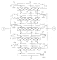
- a plasma processing apparatus of prior art 2 shown in FIG. 7 has been proposed (see, for example, Patent Document 2).
- a discharge part composed of a cathode electrode 100 connected to a power supply part E and a grounded anode electrode 200 is arranged in a plurality of upper and lower stages in a chamber.
- the lower anode electrode 200 incorporates a heater 201, and a substrate S1 is installed on the upper surface thereof.
- a reactive gas G indicated by an arrow is introduced into the cathode electrode 100, and the reactive gas is ejected from a large number of holes formed in the lower surface.
- a film is formed on the surface of the substrate S1 by generating plasma discharge between the cathode and anode electrodes in the reactive gas atmosphere.
- this plasma processing apparatus is configured as an etching apparatus by placing a substrate on a cathode electrode arranged below and arranging an anode electrode thereon. In this case, a reactive gas is introduced into the grounded anode electrode, and the reactive gas is ejected between the cathode and anode electrodes through a number of holes formed in the lower surface.
- a heater is provided in the cathode electrode connected to the power source.
- the plasma device of the prior art 2 is configured to be used in any of the film forming apparatus and the etching apparatus, in order to share the power supply unit E that supplies power to the plurality of cathode electrodes 100,
- the inter-discharge portion distance B between the discharge electrodes adjacent to the anode electrode 200 of one discharge portion and the cathode electrode 100 of another discharge portion is set to more than twice the inter-electrode distance A between the electrodes 200. .
- the anode electrode 200 exists on each cathode electrode 100 in each of the discharge units other than the uppermost stage among the plurality of discharge units. However, the anode electrode 200 does not exist on the cathode electrode 100 in the uppermost discharge part. Further, in the case of the etching plasma processing apparatus not shown, an anode electrode is present under each cathode electrode in each of the discharge parts other than the lowest stage among the plurality of discharge parts. There is no anode electrode under the cathode electrode in the discharge part. That is, the uppermost or lowermost cathode electrode is not sandwiched from above and below by the anode electrode like the other-stage cathode electrodes.
- the impedance of the uppermost or lowermost cathode electrode differs from the impedance of the cathode electrode of the other stages, and the amount of power supplied to the cathode electrodes of each stage cannot be made uniform. It is not possible to evenly arrange plasma discharges. This leads to a problem that the film formation or etching performed in the uppermost or lowermost discharge part and the film formation or etching performed in the other discharge part become non-uniform.
- the present invention has been made in view of such a problem, and an object thereof is to provide a plasma processing apparatus capable of causing uniform plasma discharge in a plurality of discharge portions.
- a reaction chamber a plurality of discharge parts that are arranged oppositely in the reaction chamber and are plasma-discharged in a reaction gas atmosphere, and a pseudo electrode
- the plurality of first electrodes are connected to the power supply unit, the plurality of second electrodes are grounded, and the pseudo electrodes are arranged opposite to each other on the outer surface side of the first electrodes on the outer side in the parallel direction among the plurality of first electrodes.
- a plasma processing apparatus in which the pseudo electrode is grounded.
- a reaction chamber, and a plurality of discharge portions each including a pair of a first electrode and a second electrode that are arranged in a reaction chamber and face each other to perform plasma discharge in a reaction gas atmosphere
- a plasma processing apparatus including a pseudo electrode disposed opposite to the outer surface of the first electrode on the outer side in the parallel direction among the plurality of first electrodes
- a substrate is set on one or more second electrodes, a plurality of second electrodes and pseudo electrodes are grounded, and power is supplied to the plurality of first electrodes, and plasma discharge is performed using a reactive gas on the substrate.
- a film forming method is provided.
- a reaction chamber, and a plurality of discharge portions that are arranged in a reaction chamber and are opposed to each other and include a first electrode and a second electrode that perform plasma discharge in a reaction gas atmosphere
- the semiconductor substrate or the semiconductor film on the substrate is etched using a plasma processing apparatus including a pseudo electrode disposed opposite to the outer surface of the first electrode on the outer side in the parallel direction among the plurality of first electrodes.
- a semiconductor substrate or a substrate having a semiconductor film is placed on one or more first electrodes, a plurality of second electrodes and pseudo electrodes are grounded, and power is supplied to the plurality of first electrodes.
- an etching method comprising etching a semiconductor substrate or a semiconductor film on the substrate by performing plasma discharge using a gas.
- the pseudo first electrode is arranged on the outer surface side of the first electrode on the outer side in the parallel direction among the plurality of first electrodes, so that the first outer electrode is the pseudo electrode and the second electrode.
- This state is the same as the state in which the other first electrodes are disposed between the two second electrodes.
- each of the plurality of first electrodes connected to the power supply unit is disposed between the grounded electrodes (between the second electrodes or between the second electrode and the pseudo electrode).
- the generated plasma discharge can be made uniform.
- the impedance of the outer first electrode can be made equal to the impedance of the other first electrode. Can be easily aligned. As a result, the film forming process or the etching process in the semiconductor element manufacturing process can be efficiently performed with high accuracy.
- Embodiment 1 of the plasma processing apparatus of this invention It is a schematic block diagram which shows Embodiment 2 of the plasma processing apparatus of this invention. It is a schematic block diagram which shows Embodiment 3 of the plasma processing apparatus of this invention. It is a schematic block diagram which shows Embodiment 4 of the plasma processing apparatus of this invention. It is a schematic block diagram which shows Embodiment 5 of the plasma processing apparatus of this invention. It is a schematic block diagram which shows Embodiment 7 of the plasma processing apparatus of this invention. It is a schematic block diagram which shows the conventional plasma processing apparatus for film-forming.
- a plasma processing apparatus includes a reaction chamber, a plurality of discharge portions that are arranged opposite to each other in the reaction chamber and perform plasma discharge in a reaction gas atmosphere, and a pseudo electrode.
- the plurality of first electrodes are connected to the power supply unit, the plurality of second electrodes are grounded, and the pseudo electrodes are arranged opposite to each other on the outer surface side of the first electrodes on the outer side in the parallel direction among the plurality of first electrodes. And the pseudo electrode is grounded.
- a plurality of discharge portions means two or more discharge portions.
- the number of discharge parts (the number of sets) is not particularly limited, and examples thereof include two, three, four, five, and six.
- the plasma processing apparatus includes a gas introduction part for introducing a reaction gas into the reaction chamber, an exhaust part for exhausting the reaction gas from the reaction chamber, a plurality of first and second electrodes, and a pseudo electrode. And further supporting means for supporting horizontally or vertically in parallel.
- the horizontal support of the plurality of first and second electrodes and the pseudo electrode means that the parallel plate-type electrodes are arranged in the vertical direction in a state where they are laid down horizontally.
- Supporting the first and second electrodes and the pseudo electrode in a vertical manner and arranging them in parallel means that the parallel plate-type electrodes are arranged in the left-right direction in a state where they are erected vertically.
- this plasma processing apparatus includes an upper and lower parallel type in which a plurality of sets of parallel plate type discharge parts (electrode bodies) each including a first electrode and a second electrode are arranged in the vertical direction, and a plurality of sets of parallel plate type discharge parts.
- electrode bodies electrode bodies
- parallel plate type discharge parts electrode bodies
- the relative positions of the first electrode and the second electrode are not limited.
- the substrate which is an object to be plasma-treated, may be placed on either the first electrode or the second electrode, and when the substrate is placed on the second electrode, the plasma for film formation
- the substrate is installed on the first electrode, it is configured as an etching plasma processing apparatus.
- the pseudo electrode is disposed opposite to the outer surface side of the first electrode outside in the parallel direction (that is, the vertical direction or the left-right direction) among the plurality of first electrodes.
- this pseudo electrode is a pseudo second electrode for arranging the outer first electrode between the two second electrodes (ground electrodes) in the same manner as the other first electrodes. .
- the impedance of the first electrode on the outer side in the parallel direction among the plurality of first electrodes can be made equal to the impedance of the other first electrode. That is, the impedances of the respective first electrodes can be made equal so that the quality of the substrates subjected to the plasma treatment by the plasma discharge in each discharge part becomes equivalent.
- the present invention also includes a plasma processing apparatus in which the outer first electrode facing the pseudo electrode and one or more other first electrodes are connected to different power supply units. In this case, since the variation in the impedance of these first electrodes is smaller than that of the plasma processing apparatus having no pseudo electrode, the impedances of these first electrodes can be more easily aligned.
- the distance between the pseudo electrode and the first electrode facing this is set to one. It is preferable that the pseudo electrode is arranged so that the distance between the second electrode of the (optional) discharge part and the first electrode of the other discharge part adjacent to the second electrode is aligned. That is, the distance between the pseudo electrode and the first electrode facing the pseudo electrode is adjusted to the distance between the discharge parts so that the quality of the plasma-treated substrate by the plasma discharge in each discharge part becomes more equal (almost identical). Preferably).
- the plasma processing apparatus includes, for example, a plasma processing apparatus (I) in which a first electrode facing a pseudo electrode and a first electrode of a discharge unit adjacent to the first electrode are connected to the same power supply unit. (See, for example, FIG. 1), and a plasma processing apparatus (II) in which a first electrode facing a pseudo electrode and a first electrode of a discharge unit not adjacent to the first electrode are connected to the same power supply unit, respectively. (For example, see FIG. 5), but is not limited thereto. In the case of (I), the case where two or more first electrodes of the discharge part adjacent to each other on the pseudo electrode side are connected to the same power supply part is also included.
- three or more discharge parts are arranged from the pseudo electrode side, and are different between the plurality of first electrodes including the first electrode facing the pseudo electrode connected to the same power supply part.
- positioned is included.
- the power supply unit one that includes a high-frequency generator and an amplifier that amplifies high-frequency power from the high-frequency generator and supplies it to the first electrode can be used.
- the connection form between the first electrode and the power supply unit in the discharge unit is not particularly limited. That is, among all the discharge units, the first electrode of one discharge unit and the first electrode of another discharge unit adjacent thereto are (a) the same high-frequency generator via the same amplifier, respectively. Or (b) each connected to the same high frequency generator via a separate amplifier, or (c) each connected to a different high frequency generator via an amplifier. In the case of connection forms (a) to (c), at least two sets of discharge parts are connected to the same power supply part.
- the second electrode of one discharge part and the other adjacent thereto with respect to the interelectrode distance A between the first electrode and the second electrode in each discharge part is defined as follows.
- the distance B between the discharge portions is set to be twice or more (B / A ⁇ 2) with respect to the distance A between the electrodes, and the distance from the pseudo electrode to the first electrode facing the discharge is the discharge. It is aligned with the inter-part distance B and is preferably set equal.
- connection form (a) corresponds to the plasma processing apparatus (I).
- connection mode (b) or (c) the inter-discharge portion distance B is set to 1.5 times or more (B / A ⁇ 1.5) with respect to the inter-electrode distance A, and from the pseudo electrode The distance to the opposing first electrode is aligned with the inter-discharge portion distance B, and is preferably set equal.
- the first electrodes of the adjacent discharge units are connected to the power supply unit via different electrical systems, so that the plasma discharge between the adjacent discharge units is connected ( It becomes more difficult to interfere with each other than in a), and the distance B between the discharge parts can be made narrower than in the connection mode (a).
- Connection modes (b) and (c) correspond to the plasma processing apparatus of (II).
- the flat plate-like first electrode, the second electrode, and the pseudo electrode which are arranged to face each other in parallel, bend due to their own weight, particularly when they are supported horizontally by the support means. This bending affects the interelectrode distance A and the distance B. Therefore, by aligning the impedances of the plurality of first electrodes with higher accuracy, the plasma discharges at the plurality of discharge portions can be uniformly aligned with higher accuracy, and the first electrode, the second electrode, and the pseudo electrode can be bent. It is desirable to consider. Therefore, the present invention can be configured as follows.
- the first electrode of the discharge unit facing (adjacent) the pseudo electrode and the first electrode of one or more other discharge units are connected to the same power supply unit, This can be applied when the first electrode of the discharge unit facing the pseudo electrode and the first electrodes of all other discharge units are connected to different power supply units.
- the second electrode and the pseudo electrode are the same in at least one of shape, size and material. It is preferable that two or more of the second electrode and the pseudo electrode are the same in shape, size, and material, and it is particularly preferable that all three are the same. (1-2) When the first electrode of one discharge section adjacent to the pseudo electrode and the first electrode of one or more other discharge sections are connected to the same power supply section, the other discharge section The second electrode and the pseudo electrode of the discharge part adjacent to each other have the same shape, size and material. These configurations are applicable to Embodiments 1 to 8 described later.
- the first electrode, the second electrode, and the pseudo electrode are configured with a shape, a size, and a material that align the respective deflection amounts.
- “equalizing the amount of bending” means that the amount of bending is substantially the same so that the plasma discharge in each discharge portion is aligned to the extent that it does not affect the quality of the workpiece.
- the same location of the first electrode is connected to the power supply unit.
- the plurality of first electrodes connected to the same power supply unit are connected to the power supply unit at the same location.
- the second electrode and the pseudo electrode have built-in heaters, and each heater can generate heat at the same temperature.
- the other discharge section It is preferable that the second electrode and the pseudo electrode of the discharge section adjacent to each have a built-in heater, and each heater can generate heat at the same temperature.
- the configurations of (1-2), (3-2), (4-2), (5-2), and (6-2) are particularly the first of the discharge part facing (adjacent) the pseudo electrode.
- the electrode and the first electrode of one or more other discharge units are connected to the same power supply unit, the impedances of the plurality of first electrodes connected to the same power supply unit are more accurately aligned. This is the preferred state.
- the amount of bending due to their own weight with respect to the second electrode and the pseudo electrode.
- the amount of deflection due to their own weight can be made close to each other.
- the inter-electrode distance A optimal for plasma discharge in each discharge part is set.
- the impedances of the plurality of first electrodes can be more accurately aligned as described above.
- the heaters in the configurations of (6-1) and (6-2) are incorporated in the second electrode in order to heat the substrate, which is an object to be processed, during plasma processing.
- a heater is also incorporated in the pseudo electrode, and during the plasma treatment, the pseudo electrode is heated in the same manner as the second electrode, preferably at the same temperature as the second electrode. To heat the pseudo electrode.
- the influence of the heat of the second electrode and the pseudo electrode can be made equal.
- by heating the second electrode and the pseudo electrode to the same temperature it is possible to equalize the influence of the deflection of the heat of each first electrode, and the first electrode between each second electrode and the pseudo electrode.
- the influence of heat deflection can be made equal, and the influence of heat deflection can be made equal.
- the impedances of the plurality of first electrodes can be aligned with higher accuracy.
- FIG. 1 is a schematic configuration diagram showing Embodiment 1 of the plasma processing apparatus of the present invention.
- the plasma processing apparatus according to the first embodiment is a vertically parallel type film forming plasma processing apparatus for forming a desired film on the surface of a substrate S1, which is an object to be processed, and reacts with a reaction chamber R and a reaction chamber R.
- a plurality of discharge portions 3 comprising a set of the first and second electrodes 2, a pseudo electrode 4, a support means 5 for supporting the plurality of first and second electrodes 1, 2 and the pseudo electrode 4 in parallel in a horizontal manner; Is provided.
- the plurality of first electrodes 1 are connected to a single power supply unit E, the plurality of second electrodes 2 are grounded, and the plurality of first electrodes 1 are arranged outside in the parallel direction.
- the pseudo electrode 4 is arranged on the outer surface side of the first electrode 1 so as to be opposed, and the pseudo electrode 4 is grounded.
- the power supply unit E includes a high-frequency generator and an amplifier that amplifies high-frequency power from the high-frequency generator and supplies the first electrode to the first electrode. Like the connection form (a), they are connected to the same high-frequency generator through the same amplifier.
- FIG. 1 illustrates a plasma processing apparatus in which the discharge units 3 are arranged in three upper and lower stages, the number of the discharge units 3 may be two or four or more.
- the first electrode 1 is referred to as a cathode electrode 1 and the second electrode 2 is referred to as an anode electrode 2.
- the reaction chamber R is configured by a sealable chamber C that houses a plurality of discharge parts 3 and pseudo electrodes 4.
- the chamber C has a box shape and is connected to the exhaust unit 6. Furthermore, support means 5 for supporting the plurality of cathode electrodes 1 and the plurality of anode electrodes 2 is formed on the inner wall surface of the chamber.
- the exhaust unit 6 includes a vacuum pump 6a, an exhaust pipe 6b connecting the vacuum pump 6a and the reaction chamber R, and a pressure controller 6c disposed between the reaction chamber R and the vacuum pump 6a in the exhaust pipe 6b.
- the support means 5 is a support piece that protrudes from the inner wall surface of the chamber C by a predetermined dimension in the horizontal direction.
- the supporting pieces are provided on the inner wall surface of the chamber C at a plurality of positions at upper and lower positions at predetermined intervals.
- the supporting pieces support the flat cathode electrode 1 and the anode electrode 2 in parallel and horizontally, and the pseudo electrode 4 horizontally.
- seven stages of support means 5 are provided to support the four corners of the lower surface of the three sets of cathode / anode electrodes 1 and 2 and the pseudo electrode 4.
- the distance between the cathode electrode 1 of another discharge part 3 adjacent to the anode electrode 2 of one discharge part 3 The support means of each stage is at a height position such that the distance B between the discharge parts is more than twice and the distance between the pseudo electrode 4 and the uppermost cathode electrode 1 is equal to the distance B between the discharge parts. 5 is arranged.
- the distance A between the electrodes is set to 2 to 30 mm
- the distance B between the discharge parts is set to 4 to 60 mm or more.
- the accuracy of the inter-electrode distance A in the plane is preferably within a few percent, and particularly preferably 1% or less.
- Each anode electrode 2 has a heater 7 inside, and a substrate S1 is installed on the upper surface, and heats the substrate S1 during film formation under plasma discharge.
- the substrate S1 is generally a silicon substrate or a glass substrate, but is not particularly limited thereto.
- Each anode 2 is made of a material having conductivity and heat resistance, such as stainless steel, aluminum alloy, and carbon.
- the dimension of each anode electrode 2 is determined to an appropriate value according to the dimension of the substrate S1 for forming a thin film.
- the dimensions of the anode electrode 2 are designed to be 1000 to 1500 mm ⁇ 600 to 1000 mm with respect to the dimensions of the substrate S1 of 900 to 1500 mm ⁇ 400 to 1200 mm.
- each anode electrode 2 controls the heating of the anode electrode 2 to room temperature to 300 ° C., for example, a sealed heating device such as a sheath heater in an aluminum alloy and a sealed temperature sensor such as a thermocouple. Can be used.
- a sealed heating device such as a sheath heater in an aluminum alloy and a sealed temperature sensor such as a thermocouple. Can be used.
- Each cathode electrode 1 is made of stainless steel or aluminum alloy.
- the dimension of each cathode electrode 1 is set to an appropriate value according to the dimension of the substrate S1 on which film formation is performed, and can be designed with the same dimensions (planar size and thickness) as the anode electrode 2. Further, each cathode electrode 1 is set to the same deflection amount (rigidity) as the anode electrode 2. In this case, the cathode electrode 1 may or may not be formed of the same shape, size and material as the anode electrode 2 as long as the deflection amount is the same.
- Each cathode electrode 1 has a hollow interior, and a plurality of through holes are drilled in the plasma discharge surface facing the paired anode electrode 2.
- This drilling process is preferably performed with a circular hole having a diameter of 0.1 mm to 2 mm at a pitch of several mm to several cm.
- a gas introduction pipe as a gas introduction part 1a is connected to one end face of each cathode electrode 1, and a gas supply source (not shown) and the gas introduction part 1a are connected by a connection pipe, and a reaction gas G1 is supplied from the gas supply source to the inside of the cathode electrode 2 and is ejected from a large number of through holes toward the surface of the substrate S1.
- the source gas for example, SiH 4 (monosilane) gas diluted with H 2 is used.
- each cathode electrode 1 power is supplied to each cathode electrode 1 by a plasma excitation power source as the power source unit E.
- a plasma excitation power source as the power source unit E.
- power for example, power of 10 W to 100 kW at a frequency of AC 1.00 MHz to 60 MHz is used, and specifically, 10 W to 10 kW is used at 13.56 MHz to 60 MHz.
- an impedance matching unit, an amplifier, and the like may be disposed in the electrical path between the power supply unit E and the cathode electrode 1.
- the pseudo electrode 4 preferably has the same amount of deflection (rigidity) as the anode electrode 2 and is made of the same material, shape and size, and the heater 7 same as the heater 7 of the anode electrode 2 is built therein. ing. That is, the pseudo electrode 4 has the same configuration as the anode electrode 2.
- the plasma processing apparatus for film formation according to Embodiment 1 has the above (1-2), (2), (3-2), (4-2), (5-2) and (6-2). It is configured as follows.
- the substrate when forming a semiconductor film on a substrate, the substrate is placed on one or more second electrodes, and a plurality of second electrodes and In a state where the pseudo electrode is grounded and electric power is supplied to the plurality of first electrodes, plasma discharge is performed using a reactive gas to form a film on the substrate.
- a glow discharge region (plasma discharge region) is generated between the cathode electrode 1 and the anode electrode 2, and an amorphous film or a crystalline film can be formed on the substrate S1.
- a SiH 4 gas diluted with H 2 as a source gas a silicon thin film having a thickness of 300 nm can be deposited with a thickness distribution within ⁇ 10%.
- each of the cathode electrodes 1 in the plurality of discharge portions 3 is in the same state disposed between the anode electrode 2 and the pseudo electrode 4, the impedance of the outer cathode electrode 1 is changed to the other cathode electrode 1.
- the impedance can be aligned in the same manner.
- the anode electrode 2 and the pseudo electrode 4 are made of the same material, shape and size, and the pseudo electrode 4 also heats the uppermost cathode electrode 1 from above at the same temperature as the anode electrode 2.
- the deflection amounts of 2, 4 are equal. Therefore, the distances A between the electrodes are equal and the distances B between the discharge parts are equal.
- each cathode electrode 1 is set to the same deflection amount as the anode electrode 2, the interelectrode distance A between the cathode electrode 1 and the anode electrode 2 is maintained with high accuracy.
- the plasma processing apparatus of the first embodiment can efficiently perform the film forming process in the semiconductor element manufacturing process with high accuracy.
- FIG. 2 is a schematic block diagram showing Embodiment 2 of the plasma processing apparatus of the present invention.
- the plasma processing apparatus of the second embodiment is also a film forming plasma processing apparatus, but is mainly different from the first embodiment (upper and lower parallel type) in that it is a left-right parallel type. That is, the plasma processing apparatus of the second embodiment has a configuration in which the plasma processing apparatus of the configuration of the first embodiment described with reference to FIG. 1 is generally laid down. As in the first embodiment, (1-2), (2 ), (3-2), (4-2), (5-2) and (6-2).
- FIG. 2 is a schematic block diagram showing Embodiment 2 of the plasma processing apparatus of the present invention.
- the plasma processing apparatus of the second embodiment is also a film forming plasma processing apparatus, but is mainly different from the first embodiment (upper and lower parallel type) in that it is a left-right parallel type. That is, the plasma processing apparatus of the second embodiment has a configuration in which the plasma processing apparatus of the configuration of the first embodiment described with reference to FIG. 1 is generally laid down
- Embodiment 2 in order to support the cathode electrode 1, the anode electrode 2 and the pseudo electrode 4 vertically, a support piece which is provided on the upper inner wall surface and the lower inner wall surface of the chamber and holds each electrode from both sides Projecting in the vertical direction constitutes a support means.
- a protrusion for holding the substrate S1 is formed on the substrate installation surface of the anode electrode 2.
- the plasma processing apparatus of the second embodiment also fills the gap between the cathode electrode 1 and the anode electrode 2 with the reaction gas G1 that is a film material at a predetermined flow rate and pressure, and the cathode electrode 1 and the anode electrode. 2, a glow discharge region (plasma discharge region) is generated between the cathode electrode 1 and the anode electrode 2 to form an amorphous film or a crystalline film on the substrate S1. can do.
- the reaction gas G1 that is a film material at a predetermined flow rate and pressure
- the plasma processing apparatus of the second embodiment since each of the cathode electrodes 1 in the plurality of discharge portions 3 is in the same state disposed between the anode electrode 2 and the pseudo electrode 4, the impedance is uniform.
- the plasma processing apparatus of the second embodiment is a left-right parallel type in which the electrodes 1, 2, and 4 are vertically supported, the influence of bending as in each electrode in the first embodiment is small, and the pseudo electrode 4 Since the cathode electrode 1 on the outside (left side in FIG. 2) is heated from the side at the same temperature as the anode electrode 2, there is almost no variation in the distance A between the electrodes and the distance B between the discharge parts. For these reasons, the plasma processing apparatus of the second embodiment can also efficiently perform the film forming process in the semiconductor element manufacturing process with high accuracy.
- FIG. 3 is a schematic block diagram showing Embodiment 3 of the plasma processing apparatus of the present invention.
- the plasma processing apparatus of the third embodiment is a vertically parallel type etching plasma processing apparatus, and includes a plurality of sets of discharge portions 13 including a cathode electrode 11 and an anode electrode 12 and a pseudo electrode 14 as in the first embodiment.
- a chamber, a support means and an exhaust part are provided.
- the main difference between the third embodiment and the first embodiment is that the cathode electrode 11 and the anode electrode 12 are arranged upside down in each discharge part 13, and the substrate S 2 is placed on the cathode electrode 11 connected to the power supply part E.
- the anode electrode 12 to be grounded is disposed above the substrate S2.
- the pseudo electrode 14 to be grounded is disposed below the lowermost cathode electrode 11.
- the anode electrode 12 of the third embodiment has a gas introduction part 12a for introducing the reaction gas G2 therein, and the reactive gas G2 is ejected on the lower surface. A number of through holes.
- the cathode electrode 11 of the third embodiment is provided with a heater 17 in the same manner as the anode electrode 2 of the first embodiment.
- the pseudo electrode 14 can have the same configuration as the anode electrode 12. However, the pseudo electrode 14 may or may not be connected to a gas supply source, and the reaction gas may not be supplied even when connected.
- the third embodiment is configured as the above (1-2), (2), (3-2), (4-2), (5-2), and (6-2). ing. Further, in the third embodiment, as in the first embodiment, the distance between the cathode electrode 11 and the anode electrode 12 in each discharge portion 13 is different from that adjacent to the cathode electrode 11 of one discharge portion 13.
- the discharge portion distance B between the discharge portion 13 and the anode electrode 12 is more than doubled, and the distance between the pseudo electrode 14 and the lowermost cathode electrode 11 is equal to the discharge portion distance B.
- the distance A between the electrodes is set to 2 to 30 mm
- the distance B between the discharge parts is set to 4 to 60 mm or more.
- the accuracy of the inter-electrode distance A in the plane is preferably within a few percent, and particularly preferably 1% or less.
- etching a semiconductor substrate or a semiconductor film on the substrate when etching a semiconductor substrate or a semiconductor film on the substrate, a semiconductor substrate or a substrate having a semiconductor film is placed on one or more first electrodes.
- the semiconductor substrate or the semiconductor film on the substrate is etched by performing plasma discharge using a reactive gas while grounding the plurality of second electrodes and the pseudo electrode and supplying power to the plurality of first electrodes.
- a reaction gas G2 which is an etching gas obtained by diluting a fluorine-based gas with an inert gas such as argon, is filled in the gap between the cathode electrode 11 and the anode electrode 12 at a predetermined flow rate and pressure, and the cathode electrode
- a glow discharge region plasma discharge region
- the substrate S2 for example, a silicon substrate
- Etching can be efficiently performed at a rate of.
- each of the cathode electrodes 11 in the plurality of discharge portions 13 is in the same state disposed between the anode electrode 12 and the pseudo electrode 14, the impedance is uniform. Further, the anode electrode 12 and the pseudo electrode 14 are configured with the same material, shape and size, and the pseudo electrode 14 is also heated by the cathode electrode 11 at the lowest stage. The distances A between the electrodes are equal and the distances B between the discharge parts are equal. Furthermore, since the cathode electrode 11 and the anode electrode 2 are set to the same deflection amount, the interelectrode distance A between the cathode electrode 1 and the anode electrode 2 is maintained with high accuracy. From these things, the etching process in the manufacturing process of a semiconductor element can be efficiently performed with high accuracy by the plasma processing apparatus of the third embodiment.
- FIG. 4 is a schematic block diagram showing Embodiment 4 of the plasma processing apparatus of the present invention.
- the plasma processing apparatus of the fourth embodiment is also an etching plasma processing apparatus, but is mainly different from the third embodiment (upper and lower parallel type) in that it is a left-right parallel type. That is, the plasma processing apparatus according to the fourth embodiment has a configuration in which the plasma processing apparatus according to the third embodiment described with reference to FIG.
- the plasma processing apparatus includes a plurality of sets of discharge units 13 each including a cathode electrode 11 and an anode electrode 12 and a pseudo electrode 14, and includes a chamber, a support unit, and an exhaust unit (not shown). ing.
- a support piece that is provided on the upper inner wall surface and the lower inner wall surface of the chamber and sandwiches each electrode from both sides. Projecting in the vertical direction constitutes a support means.
- a projection for holding the substrate S2 is formed on the substrate installation surface of the anode electrode 12.
- the fourth embodiment is configured as the above (1-2), (2), (3-2), (4-2), (5-2), and (6-2). ing.
- the plasma processing apparatus according to the fourth embodiment also uses, for example, the reaction gas G2, which is an etching gas obtained by diluting a fluorine-based gas with an inert gas such as argon, at a predetermined flow rate and pressure at the cathode electrode 11.
- the reaction gas G2 which is an etching gas obtained by diluting a fluorine-based gas with an inert gas such as argon, at a predetermined flow rate and pressure at the cathode electrode 11.
- a gap between the cathode electrode 11 and the anode electrode 12 is filled, and a high frequency power is applied to the cathode electrode 11 and the anode electrode 12 to generate a glow discharge region (plasma discharge region) between the cathode electrode 11 and the anode electrode 12.
- the substrate S2 (for example, a silicon substrate) can be efficiently etched at a rate of
- each of the cathode electrodes 11 in the plurality of discharge portions 13 is in the same state disposed between the anode electrode 12 and the pseudo electrode 14, the impedance is uniform.
- the plasma processing apparatus of the fourth embodiment is a left-right parallel type in which the electrodes 11, 12, and 14 are vertically supported, the influence of bending as in each electrode in the third embodiment is small, and the pseudo electrode 14 is also included. Since heating is performed by the cathode electrode 11 on the outer side (left side in FIG. 3), the distances A between the electrodes are equal and the distances B between the discharge parts are equal. From these things, the etching process in the manufacturing process of a semiconductor element can be efficiently performed with high accuracy by the plasma processing apparatus of the third embodiment.
- FIG. 5 is a schematic block diagram showing Embodiment 5 of the plasma processing apparatus of the present invention.
- the plasma processing apparatus of the fifth embodiment is the same vertical and vertical type film forming plasma processing apparatus as that of the first embodiment shown in FIG. 1, and the connection mode between the plurality of cathode electrodes 1 and the power supply unit E is mainly the embodiment.
- the configuration is the same except that it is different from 1.
- the cathode electrodes 1 in at least two sets of discharge units 3 are connected to the same power supply unit E, and the cathode electrodes 1 of adjacent discharge units 3 are connected to each other in the connection form (b ) Are connected to the same high-frequency generator via individual amplifiers, or are connected to different high-frequency generators via amplifiers as in connection mode (c). That is, the cathode electrodes 1 of the adjacent discharge units 3 are connected to the power supply unit E via different electrical systems. In FIG. 5, two power supply units E are drawn, but this is not necessarily intended to use separate high frequency generators. Thus, by connecting each cathode electrode 1 to the power supply unit E, the distance B between the discharge units is 1.5 times or more the distance A between the electrodes, which is narrower than that of the first embodiment.
- the relative positional relationship between the cathode electrode 1 and the feeding position is the same, and the relative positional relationship between the anode electrode 2 and the grounding position.
- the relative positional relationship is the same means that the feeding position when the cathode electrode 1 is viewed in plan is the same for each cathode electrode 1 and the anode electrode 2 is viewed in plan. This means that the grounding position is the same for each anode electrode 2. If it does in this way, in the some discharge part 3 connected by the same electrical system, electric power can be more uniformly supplied with respect to each cathode electrode 1 from the power supply part E.
- the fifth embodiment is similar to the first embodiment as in the above (1-2), (2), (3-2), (4-2), (5-2), and (6-2). It is configured.
- (1), (3-2), (4-2), (5-2), and (6-2) will be described in detail.
- the middle (third from the top) discharge portion in FIG. Reference numeral 3 denotes an environment in which the upper and lower sides are sandwiched between the second and fourth discharge units 3 connected to a different power supply unit E. Since the first discharge part 3 is preferably in the same environment as the third discharge part 3, the pseudo electrode 4 facing the first electrode 1 of the first discharge part 3 is the first discharge part 3.
- the pseudo electrode 4 is not limited to the second electrode 2 of the second discharge unit 3, and may be the same as the second electrode 2 of the fourth discharge unit 3.
- the discharge units connected to different power supply units E may have the same or different configuration of the first electrode 1 and may have the same or different configuration of the second electrode.
- the upper and lower parallel type film forming plasma processing apparatus has been described with reference to FIG. 5, it may be a left and right parallel type film forming plasma processing apparatus having a structure that is generally laid down (not shown).
- the sixth embodiment is configured as the above (1-2), (2), (3-2), (4-2), (5-2), and (6-2). ing.
- FIG. 6 is a schematic block diagram showing Embodiment 7 of the plasma processing apparatus of the present invention.
- the plasma processing apparatus of the sixth embodiment is a vertically parallel type etching plasma processing apparatus, and has the same configuration except that the connection form of the plurality of cathode electrodes 11 and the power supply unit E is mainly different from that of the third embodiment. .
- the cathode electrodes 11 in at least two sets of discharge units 13 are connected to the same power supply unit E, and the cathode electrodes 11 of the adjacent discharge units 13 are connected to each other in the connection form (b ) Are connected to the same high-frequency generator via individual amplifiers, or are connected to different high-frequency generators via amplifiers as in connection mode (c). That is, the cathode electrodes 11 of the adjacent discharge units 13 are connected to the power supply unit E via different electrical systems. In FIG. 6, two power supply units E are drawn, but these are not necessarily intended to be individual power supply units. Thus, by connecting each cathode electrode 11 with the power supply part E, the distance B between discharge parts with respect to the distance A between electrodes can be 1.5 times or more narrower than Embodiment 3.
- the relative positional relationship between each cathode electrode 11 and the feeding position is the same, and the relative positional relationship between each anode electrode 12 and the grounding position.
- the relative positional relationship is the same means that the feeding position when the cathode electrode 11 is viewed in plan is the same for each cathode electrode 11 and the anode electrode 12 is viewed in plan.
- power can be more evenly supplied from the power supply unit E to the respective cathode electrodes 11 in the plurality of discharge units 13 connected by the same electrical system. That is, in the seventh embodiment, as in the first embodiment, as in (1-2), (2), (3-2), (4-2), (5-2), and (6-2), It is configured.
- the upper and lower parallel type etching plasma processing apparatus has been described with reference to FIG. 6, it may be a left and right parallel etching plasma processing apparatus having a structure that is generally laid down (not shown).
- the eighth embodiment is configured as the above (1-2), (2), (3-2), (4-2), (5-2), and (6-2). ing.
- the first electrode of the discharge unit facing (adjacent) the pseudo electrode and the first electrode of one or more other discharge units are connected to the same power supply unit.
- the first electrode of the discharge unit facing the pseudo electrode and the first electrodes of all other discharge units may be connected to different power supply units.
- the plasma processing apparatus of the present invention can be applied to, for example, a CVD apparatus used in a film forming process or a RIE apparatus used in an etching process in a manufacturing process of various semiconductor elements such as solar cells, TFTs, and photoreceptors. .
Abstract
A plasma processing apparatus is provided with: a reaction chamber; a plurality of discharge sections composed of a pair of a first electrode and a second electrode which are arranged to face each other in the reaction chamber so as to discharge plasma under reaction gas atmosphere; and a pseudo electrode. A plurality of first electrodes are connected to a power supply section and a plurality of second electrodes are grounded. The pseudo electrode is arranged on the outer surface side of the first electrode on the outer side in the parallel direction among the first electrodes so as to face the first electrode, and the pseudo electrode is grounded.
Description
本発明は、プラズマ処理装置、それを用いた成膜方法およびエッチング方法に関する。さらに詳しくは、プラズマ放電を起こさせる第1電極と第2電極がチャンバー内に複数組設置されてなるプラズマ処理装置の構造に関する。
The present invention relates to a plasma processing apparatus, a film forming method using the same, and an etching method. More specifically, the present invention relates to a structure of a plasma processing apparatus in which a plurality of first and second electrodes that cause plasma discharge are installed in a chamber.
従来のプラズマ処理装置として、電極間でプラズマ放電を起こさせる放電部が、チャンバー内に上下複数組配置された従来技術1のプラズマ処理装置が公知である(例えば、特許文献1参照)。
このプラズマ処理装置は、高周波電源と接続された電極と接地された電極が交互に配置されている。さらに、このプラズマ処理装置において、最上段を除く各段の電極は内部にヒータを有すると共に、最下段を除く各段の電極は、内部に反応性ガスが供給されて各電極間に反応性ガスが噴出するように構成されている。 As a conventional plasma processing apparatus, a plasma processing apparatus of theprior art 1 in which a plurality of discharge units that cause plasma discharge between electrodes is arranged in a chamber is known (see, for example, Patent Document 1).
In this plasma processing apparatus, electrodes connected to a high-frequency power source and electrodes that are grounded are alternately arranged. Further, in this plasma processing apparatus, each stage electrode except the uppermost stage has a heater inside, and each stage electrode other than the lowermost stage is supplied with a reactive gas therein, and a reactive gas is provided between the electrodes. Is configured to erupt.
このプラズマ処理装置は、高周波電源と接続された電極と接地された電極が交互に配置されている。さらに、このプラズマ処理装置において、最上段を除く各段の電極は内部にヒータを有すると共に、最下段を除く各段の電極は、内部に反応性ガスが供給されて各電極間に反応性ガスが噴出するように構成されている。 As a conventional plasma processing apparatus, a plasma processing apparatus of the
In this plasma processing apparatus, electrodes connected to a high-frequency power source and electrodes that are grounded are alternately arranged. Further, in this plasma processing apparatus, each stage electrode except the uppermost stage has a heater inside, and each stage electrode other than the lowermost stage is supplied with a reactive gas therein, and a reactive gas is provided between the electrodes. Is configured to erupt.
このように構成された従来技術1のプラズマ処理装置によれば、最上段を除く各段の電極上に基板が設置され、反応性ガスが充填された各電極間でプラズマ放電が生じることによって、基板表面に成膜あるいはエッチング処理が施される。
しかしながら、従来技術1のプラズマ処理装置は、カソード電極とアノード電極とを区別することなく基板が設置され、プラズマ放電も隣り合うすべての電極同士の間で起きるように構成されているため、以下の問題が生じる。
(1)成膜に関しては、カソード電極上で形成された膜とアノード電極上で形成された膜とが混在してしまう。一方、エッチングに関しては、カソード電極上でエッチングされた基板とアノード電極上でエッチングされた基板とが混在してしまう。こられのことは、成膜に適さないカソード電極上へのプロセスを用いるために品質の悪い膜が形成されたり、エッチングに適さないアノード電極上へのプロセスを用いるために不適切なエッチング処理が行われるという、好ましくない結果を招く。
(2)成膜時またはエッチング時に、成膜またはエッチングに適さない電極上へ基板を設置しないことにより前記(1)の問題は解消できるが、各電極間で生じるプラズマ放電を制御することはできない。この結果、隣接する放電部同士の相互干渉が起きるため、各放電部でのプラズマ放電が極めて不安定になる。 According to the plasma processing apparatus of theprior art 1 configured as described above, a substrate is installed on each stage electrode except the uppermost stage, and a plasma discharge is generated between each electrode filled with a reactive gas. A film formation or etching process is performed on the substrate surface.
However, since the plasma processing apparatus of Prior Art 1 is configured such that the substrate is installed without distinguishing between the cathode electrode and the anode electrode, and plasma discharge also occurs between all adjacent electrodes, Problems arise.
(1) Regarding film formation, a film formed on the cathode electrode and a film formed on the anode electrode are mixed. On the other hand, with respect to etching, a substrate etched on the cathode electrode and a substrate etched on the anode electrode are mixed. This means that a poor quality film is formed because a process on the cathode electrode that is not suitable for film formation is used, or an inappropriate etching process is performed because a process on the anode electrode that is not suitable for etching is used. Doing so will lead to undesirable results.
(2) The problem of (1) above can be solved by not placing a substrate on an electrode that is not suitable for film formation or etching during film formation or etching, but the plasma discharge generated between the electrodes cannot be controlled. . As a result, mutual interference between adjacent discharge parts occurs, so that plasma discharge in each discharge part becomes extremely unstable.
しかしながら、従来技術1のプラズマ処理装置は、カソード電極とアノード電極とを区別することなく基板が設置され、プラズマ放電も隣り合うすべての電極同士の間で起きるように構成されているため、以下の問題が生じる。
(1)成膜に関しては、カソード電極上で形成された膜とアノード電極上で形成された膜とが混在してしまう。一方、エッチングに関しては、カソード電極上でエッチングされた基板とアノード電極上でエッチングされた基板とが混在してしまう。こられのことは、成膜に適さないカソード電極上へのプロセスを用いるために品質の悪い膜が形成されたり、エッチングに適さないアノード電極上へのプロセスを用いるために不適切なエッチング処理が行われるという、好ましくない結果を招く。
(2)成膜時またはエッチング時に、成膜またはエッチングに適さない電極上へ基板を設置しないことにより前記(1)の問題は解消できるが、各電極間で生じるプラズマ放電を制御することはできない。この結果、隣接する放電部同士の相互干渉が起きるため、各放電部でのプラズマ放電が極めて不安定になる。 According to the plasma processing apparatus of the
However, since the plasma processing apparatus of Prior Art 1 is configured such that the substrate is installed without distinguishing between the cathode electrode and the anode electrode, and plasma discharge also occurs between all adjacent electrodes, Problems arise.
(1) Regarding film formation, a film formed on the cathode electrode and a film formed on the anode electrode are mixed. On the other hand, with respect to etching, a substrate etched on the cathode electrode and a substrate etched on the anode electrode are mixed. This means that a poor quality film is formed because a process on the cathode electrode that is not suitable for film formation is used, or an inappropriate etching process is performed because a process on the anode electrode that is not suitable for etching is used. Doing so will lead to undesirable results.
(2) The problem of (1) above can be solved by not placing a substrate on an electrode that is not suitable for film formation or etching during film formation or etching, but the plasma discharge generated between the electrodes cannot be controlled. . As a result, mutual interference between adjacent discharge parts occurs, so that plasma discharge in each discharge part becomes extremely unstable.
このような問題を解消するために、図7に示す従来技術2のプラズマ処理装置が提案されている(例えば、特許文献2参照)。
このプラズマ処理装置は、例えば、電源部Eと接続されるカソード電極100および接地されるアノード電極200からなる放電部が、チャンバー内に上下複数段で配置される。下側のアノード電極200は、ヒータ201を内蔵すると共に、その上面に基板S1が設置される。一方、カソード電極100は、内部に矢印で示す反応性ガスGが導入され、下面に形成された多数の孔から反応性ガスを噴出する。そして、反応性ガス雰囲気下のカソード・アノード電極間でプラズマ放電が発生することにより基板S1の表面に膜が形成される。
また、図示省略するが、このプラズマ処理装置は、下に配置したカソード電極上に基板を設置し、上にアノード電極を配置することにより、エッチング装置として構成される。この場合、接地されるアノード電極内に反応性ガスが導入され、下面に形成された多数の孔からカソード・アノード電極間に反応性ガスを噴出する。また、電源と接続されるカソード電極内にヒータが設けられる。 In order to solve such a problem, a plasma processing apparatus ofprior art 2 shown in FIG. 7 has been proposed (see, for example, Patent Document 2).
In this plasma processing apparatus, for example, a discharge part composed of acathode electrode 100 connected to a power supply part E and a grounded anode electrode 200 is arranged in a plurality of upper and lower stages in a chamber. The lower anode electrode 200 incorporates a heater 201, and a substrate S1 is installed on the upper surface thereof. On the other hand, a reactive gas G indicated by an arrow is introduced into the cathode electrode 100, and the reactive gas is ejected from a large number of holes formed in the lower surface. A film is formed on the surface of the substrate S1 by generating plasma discharge between the cathode and anode electrodes in the reactive gas atmosphere.
Although not shown, this plasma processing apparatus is configured as an etching apparatus by placing a substrate on a cathode electrode arranged below and arranging an anode electrode thereon. In this case, a reactive gas is introduced into the grounded anode electrode, and the reactive gas is ejected between the cathode and anode electrodes through a number of holes formed in the lower surface. A heater is provided in the cathode electrode connected to the power source.
このプラズマ処理装置は、例えば、電源部Eと接続されるカソード電極100および接地されるアノード電極200からなる放電部が、チャンバー内に上下複数段で配置される。下側のアノード電極200は、ヒータ201を内蔵すると共に、その上面に基板S1が設置される。一方、カソード電極100は、内部に矢印で示す反応性ガスGが導入され、下面に形成された多数の孔から反応性ガスを噴出する。そして、反応性ガス雰囲気下のカソード・アノード電極間でプラズマ放電が発生することにより基板S1の表面に膜が形成される。
また、図示省略するが、このプラズマ処理装置は、下に配置したカソード電極上に基板を設置し、上にアノード電極を配置することにより、エッチング装置として構成される。この場合、接地されるアノード電極内に反応性ガスが導入され、下面に形成された多数の孔からカソード・アノード電極間に反応性ガスを噴出する。また、電源と接続されるカソード電極内にヒータが設けられる。 In order to solve such a problem, a plasma processing apparatus of
In this plasma processing apparatus, for example, a discharge part composed of a
Although not shown, this plasma processing apparatus is configured as an etching apparatus by placing a substrate on a cathode electrode arranged below and arranging an anode electrode thereon. In this case, a reactive gas is introduced into the grounded anode electrode, and the reactive gas is ejected between the cathode and anode electrodes through a number of holes formed in the lower surface. A heater is provided in the cathode electrode connected to the power source.
さらに、従来技術2のプラズマ装置は、成膜装置とエッチング装置のいずれに構成される場合でも、複数のカソード電極100に電力を供給する電源部Eを共有化するために、カソード電極100とアノード電極200の間の電極間距離Aに対して、一の放電部のアノード電極200に隣接する他の放電部のカソード電極100との間の放電部間距離Bを2倍以上に設定している。放電部間距離Bを電極間距離Aの2倍以上とすることにより、チャンバー内で複数の放電部が存在してもこれらが相互に干渉することが防止され、成膜またはエッチングが均一で行われるようにしている。
Further, the plasma device of the prior art 2 is configured to be used in any of the film forming apparatus and the etching apparatus, in order to share the power supply unit E that supplies power to the plurality of cathode electrodes 100, The inter-discharge portion distance B between the discharge electrodes adjacent to the anode electrode 200 of one discharge portion and the cathode electrode 100 of another discharge portion is set to more than twice the inter-electrode distance A between the electrodes 200. . By making the distance B between the discharge parts more than twice the distance A between the electrodes, even if there are a plurality of discharge parts in the chamber, they are prevented from interfering with each other, and film formation or etching is performed uniformly. It is supposed to be.
しかしながら、図7で示した成膜用プラズマ処理装置の場合、複数の放電部のうちの最上段以外の各段の放電部において、各カソード電極100の上にはアノード電極200が存在しているが、最上段の放電部におけるカソード電極100の上にはアノード電極200が存在しない。
また、図示省略のエッチング用プラズマ処理装置の場合、複数の放電部のうちの最下段以外の各段の放電部において、各カソード電極の下にはアノード電極が存在しているが、最下段の放電部におけるカソード電極の下にはアノード電極が存在しない。
つまり、最上段または最下段のカソード電極は、他の段のカソード電極のようにアノード電極で上下から挟まれていない。そのため、最上段または最下段のカソード電極についてのインピーダンスが、他の段のカソード電極についてのインピーダンスと異なってしまい、各段のカソード電極への給電量を均一に揃えることができないため、各放電部でのプラズマ放電を均一に揃えることができない。このことは、最上段または最下段の放電部にて行われた成膜またはエッチングと、他の段の放電部にて行われた成膜またはエッチングとが不均一になるという問題に繋がる。 However, in the case of the film-forming plasma processing apparatus shown in FIG. 7, theanode electrode 200 exists on each cathode electrode 100 in each of the discharge units other than the uppermost stage among the plurality of discharge units. However, the anode electrode 200 does not exist on the cathode electrode 100 in the uppermost discharge part.
Further, in the case of the etching plasma processing apparatus not shown, an anode electrode is present under each cathode electrode in each of the discharge parts other than the lowest stage among the plurality of discharge parts. There is no anode electrode under the cathode electrode in the discharge part.
That is, the uppermost or lowermost cathode electrode is not sandwiched from above and below by the anode electrode like the other-stage cathode electrodes. For this reason, the impedance of the uppermost or lowermost cathode electrode differs from the impedance of the cathode electrode of the other stages, and the amount of power supplied to the cathode electrodes of each stage cannot be made uniform. It is not possible to evenly arrange plasma discharges. This leads to a problem that the film formation or etching performed in the uppermost or lowermost discharge part and the film formation or etching performed in the other discharge part become non-uniform.
また、図示省略のエッチング用プラズマ処理装置の場合、複数の放電部のうちの最下段以外の各段の放電部において、各カソード電極の下にはアノード電極が存在しているが、最下段の放電部におけるカソード電極の下にはアノード電極が存在しない。
つまり、最上段または最下段のカソード電極は、他の段のカソード電極のようにアノード電極で上下から挟まれていない。そのため、最上段または最下段のカソード電極についてのインピーダンスが、他の段のカソード電極についてのインピーダンスと異なってしまい、各段のカソード電極への給電量を均一に揃えることができないため、各放電部でのプラズマ放電を均一に揃えることができない。このことは、最上段または最下段の放電部にて行われた成膜またはエッチングと、他の段の放電部にて行われた成膜またはエッチングとが不均一になるという問題に繋がる。 However, in the case of the film-forming plasma processing apparatus shown in FIG. 7, the
Further, in the case of the etching plasma processing apparatus not shown, an anode electrode is present under each cathode electrode in each of the discharge parts other than the lowest stage among the plurality of discharge parts. There is no anode electrode under the cathode electrode in the discharge part.
That is, the uppermost or lowermost cathode electrode is not sandwiched from above and below by the anode electrode like the other-stage cathode electrodes. For this reason, the impedance of the uppermost or lowermost cathode electrode differs from the impedance of the cathode electrode of the other stages, and the amount of power supplied to the cathode electrodes of each stage cannot be made uniform. It is not possible to evenly arrange plasma discharges. This leads to a problem that the film formation or etching performed in the uppermost or lowermost discharge part and the film formation or etching performed in the other discharge part become non-uniform.
本発明は、このような問題に鑑みなされたものであり、複数の放電部において均一なプラズマ放電を起こすことができるプラズマ処理装置を提供することを目的とする。
The present invention has been made in view of such a problem, and an object thereof is to provide a plasma processing apparatus capable of causing uniform plasma discharge in a plurality of discharge portions.
かくして、本発明によれば、反応室と、反応室内に対向状に配置されて反応ガス雰囲気下でプラズマ放電させる第1電極および第2電極の組からなる複数の放電部と、擬似電極とを備え、複数の第1電極は電源部に接続され、複数の第2電極は接地され、複数の第1電極のうちの並列方向外側の第1電極の外面側に対向状に擬似電極が配置され、かつ擬似電極が接地されているプラズマ処理装置が提供される。
Thus, according to the present invention, a reaction chamber, a plurality of discharge parts that are arranged oppositely in the reaction chamber and are plasma-discharged in a reaction gas atmosphere, and a pseudo electrode, The plurality of first electrodes are connected to the power supply unit, the plurality of second electrodes are grounded, and the pseudo electrodes are arranged opposite to each other on the outer surface side of the first electrodes on the outer side in the parallel direction among the plurality of first electrodes. And a plasma processing apparatus in which the pseudo electrode is grounded.
また、本発明の別の観点によれば、反応室と、反応室内に対向状に配置されて反応ガス雰囲気下でプラズマ放電させる第1電極および第2電極の組からなる複数の放電部と、複数の第1電極のうちの並列方向外側の第1電極の外面側に対向状に配置された擬似電極とを備えたプラズマ処理装置を用いて、基板上に半導体膜を成膜する際に、1つ以上の第2電極に基板を設置し、複数の第2電極および擬似電極を接地し、かつ複数の第1電極に電力を供給した状態で、反応ガスを用いてプラズマ放電させて基板上に成膜することからなる成膜方法が提供される。
Further, according to another aspect of the present invention, a reaction chamber, and a plurality of discharge portions each including a pair of a first electrode and a second electrode that are arranged in a reaction chamber and face each other to perform plasma discharge in a reaction gas atmosphere, When forming a semiconductor film on a substrate using a plasma processing apparatus including a pseudo electrode disposed opposite to the outer surface of the first electrode on the outer side in the parallel direction among the plurality of first electrodes, A substrate is set on one or more second electrodes, a plurality of second electrodes and pseudo electrodes are grounded, and power is supplied to the plurality of first electrodes, and plasma discharge is performed using a reactive gas on the substrate. A film forming method is provided.
また、本発明のさらに別の観点によれば、反応室と、反応室内に対向状に配置されて反応ガス雰囲気下でプラズマ放電させる第1電極および第2電極の組からなる複数の放電部と、複数の第1電極のうちの並列方向外側の第1電極の外面側に対向状に配置された擬似電極とを備えたプラズマ処理装置を用いて、半導体基板または基板上の半導体膜をエッチングする際に、1つ以上の第1電極に半導体基板または半導体膜を有する基板を設置し、複数の第2電極および擬似電極を接地し、かつ複数の第1電極に電力を供給した状態で、反応ガスを用いてプラズマ放電させて半導体基板または基板上の半導体膜をエッチングすることからなるエッチング方法が提供される。
According to still another aspect of the present invention, a reaction chamber, and a plurality of discharge portions that are arranged in a reaction chamber and are opposed to each other and include a first electrode and a second electrode that perform plasma discharge in a reaction gas atmosphere, The semiconductor substrate or the semiconductor film on the substrate is etched using a plasma processing apparatus including a pseudo electrode disposed opposite to the outer surface of the first electrode on the outer side in the parallel direction among the plurality of first electrodes. In the reaction, a semiconductor substrate or a substrate having a semiconductor film is placed on one or more first electrodes, a plurality of second electrodes and pseudo electrodes are grounded, and power is supplied to the plurality of first electrodes. There is provided an etching method comprising etching a semiconductor substrate or a semiconductor film on the substrate by performing plasma discharge using a gas.
本発明によれば、複数の第1電極のうちの並列方向外側の第1電極の外面側に対向状に擬似電極が配置されることにより、この外側の第1電極は擬似電極と第2電極との間に配置された状態となり、この状態は、その他の第1電極が2つの第2電極の間に配置された状態と同じ状態である。
つまり、電源部に接続された複数の第1電極のそれぞれは、接地された電極間(第2電極間または第2電極と擬似電極の間)に配置されているため、複数の放電部にて生じるプラズマ放電を均一な状態に揃えることができる。
特に、図7に示す従来技術2のように、複数の第1電極のうちの並列方向外側の第1電極と他の電極とが、同一の電源部に接続されている場合、電源部の調整を行っても外側の第1電極のインピーダンスを他の第1電極のインピーダンスに揃えることが困難であったが、本発明によれば、外側の第1電極のインピーダンスを他の第1電極のインピーダンスに容易に揃えることができる。
この結果、半導体素子の製造プロセスにおける成膜工程またはエッチング工程を高精度に効率よく行うことができる。 According to the present invention, the pseudo first electrode is arranged on the outer surface side of the first electrode on the outer side in the parallel direction among the plurality of first electrodes, so that the first outer electrode is the pseudo electrode and the second electrode. This state is the same as the state in which the other first electrodes are disposed between the two second electrodes.
In other words, each of the plurality of first electrodes connected to the power supply unit is disposed between the grounded electrodes (between the second electrodes or between the second electrode and the pseudo electrode). The generated plasma discharge can be made uniform.
In particular, as in therelated art 2 shown in FIG. 7, when the first electrode on the outer side in the parallel direction and the other electrodes among the plurality of first electrodes are connected to the same power supply unit, the adjustment of the power supply unit However, according to the present invention, the impedance of the outer first electrode can be made equal to the impedance of the other first electrode. Can be easily aligned.
As a result, the film forming process or the etching process in the semiconductor element manufacturing process can be efficiently performed with high accuracy.
つまり、電源部に接続された複数の第1電極のそれぞれは、接地された電極間(第2電極間または第2電極と擬似電極の間)に配置されているため、複数の放電部にて生じるプラズマ放電を均一な状態に揃えることができる。
特に、図7に示す従来技術2のように、複数の第1電極のうちの並列方向外側の第1電極と他の電極とが、同一の電源部に接続されている場合、電源部の調整を行っても外側の第1電極のインピーダンスを他の第1電極のインピーダンスに揃えることが困難であったが、本発明によれば、外側の第1電極のインピーダンスを他の第1電極のインピーダンスに容易に揃えることができる。
この結果、半導体素子の製造プロセスにおける成膜工程またはエッチング工程を高精度に効率よく行うことができる。 According to the present invention, the pseudo first electrode is arranged on the outer surface side of the first electrode on the outer side in the parallel direction among the plurality of first electrodes, so that the first outer electrode is the pseudo electrode and the second electrode. This state is the same as the state in which the other first electrodes are disposed between the two second electrodes.
In other words, each of the plurality of first electrodes connected to the power supply unit is disposed between the grounded electrodes (between the second electrodes or between the second electrode and the pseudo electrode). The generated plasma discharge can be made uniform.
In particular, as in the
As a result, the film forming process or the etching process in the semiconductor element manufacturing process can be efficiently performed with high accuracy.
本発明のプラズマ処理装置は、反応室と、反応室内に対向状に配置されて反応ガス雰囲気下でプラズマ放電させる第1電極および第2電極の組からなる複数の放電部と、擬似電極とを備え、複数の第1電極は電源部に接続され、複数の第2電極は接地され、複数の第1電極のうちの並列方向外側の第1電極の外面側に対向状に擬似電極が配置され、かつ擬似電極が接地されている。
ここで、「複数の放電部」とは2つ以上の放電部を意味する。放電部の数(組数)は、特に限定されず、例えば2つ、3つ、4つ、5つ、6つ等が挙げられる。 A plasma processing apparatus according to the present invention includes a reaction chamber, a plurality of discharge portions that are arranged opposite to each other in the reaction chamber and perform plasma discharge in a reaction gas atmosphere, and a pseudo electrode. The plurality of first electrodes are connected to the power supply unit, the plurality of second electrodes are grounded, and the pseudo electrodes are arranged opposite to each other on the outer surface side of the first electrodes on the outer side in the parallel direction among the plurality of first electrodes. And the pseudo electrode is grounded.
Here, “a plurality of discharge portions” means two or more discharge portions. The number of discharge parts (the number of sets) is not particularly limited, and examples thereof include two, three, four, five, and six.
より具体的に説明すると、このプラズマ処理装置は、反応室に反応ガスを導入するガス導入部と、反応室から反応ガスを排気する排気部と、複数の第1・第2電極と擬似電極を水平状または垂直状に支持しかつ並列させる支持手段とをさらに備える。
ここで、複数の第1・第2電極と擬似電極を水平状に支持しかつ並列させるとは、平行平板型の各電極を水平状に寝かせた状態で上下方向に並べることを意味し、複数の第1・第2電極と擬似電極を垂直状に支持しかつ並列させるとは、平行平板型の各電極を垂直状に立てた状態で左右方向に並べることを意味する。すなわち、このプラズマ処理装置は、第1電極および第2電極からなる平行平板型の放電部(電極体)の複数組を上下方向に並べた上下並列タイプと、平行平板型の放電部の複数組を左右方向に並列した左右並列タイプの両方に適用できるプラズマ処理装置である。
また、本発明において、第1電極と第2電極との相対的な位置は限定されるものではない。つまり、本発明は、プラズマ処理される被処理物である基板が、第1電極と第2電極のどちら側に設置されてもよく、第2電極に基板が設置される場合は成膜用プラズマ処理装置として構成され、第1電極に基板が設置される場合はエッチング用プラズマ処理装置として構成される。 More specifically, the plasma processing apparatus includes a gas introduction part for introducing a reaction gas into the reaction chamber, an exhaust part for exhausting the reaction gas from the reaction chamber, a plurality of first and second electrodes, and a pseudo electrode. And further supporting means for supporting horizontally or vertically in parallel.
Here, the horizontal support of the plurality of first and second electrodes and the pseudo electrode means that the parallel plate-type electrodes are arranged in the vertical direction in a state where they are laid down horizontally. Supporting the first and second electrodes and the pseudo electrode in a vertical manner and arranging them in parallel means that the parallel plate-type electrodes are arranged in the left-right direction in a state where they are erected vertically. That is, this plasma processing apparatus includes an upper and lower parallel type in which a plurality of sets of parallel plate type discharge parts (electrode bodies) each including a first electrode and a second electrode are arranged in the vertical direction, and a plurality of sets of parallel plate type discharge parts. Is a plasma processing apparatus that can be applied to both a left-right parallel type in which the two are parallel in the left-right direction.
In the present invention, the relative positions of the first electrode and the second electrode are not limited. That is, according to the present invention, the substrate, which is an object to be plasma-treated, may be placed on either the first electrode or the second electrode, and when the substrate is placed on the second electrode, the plasma for film formation When the substrate is installed on the first electrode, it is configured as an etching plasma processing apparatus.
このプラズマ処理装置は、上述のように、複数の第1電極のうちの並列方向(すなわち、上下方向または左右方向)の外側の第1電極の外面側に、擬似電極が対向して配置されている。つまり、この擬似電極は、外側の第1電極が、他の第1電極と同じように2枚の第2電極(接地電極)の間に配置されるようにするための擬似第2電極である。
このようにして擬似電極を配置することにより、複数の第1電極のうちの並列方向外側の第1電極についてのインピーダンスを、他の第1電極のインピーダンスに揃えることができる。つまり、各放電部でのプラズマ放電によりプラズマ処理された基板の品質が同等となるように、各第1電極のインピーダンスを同等に揃えることができる。 In this plasma processing apparatus, as described above, the pseudo electrode is disposed opposite to the outer surface side of the first electrode outside in the parallel direction (that is, the vertical direction or the left-right direction) among the plurality of first electrodes. Yes. In other words, this pseudo electrode is a pseudo second electrode for arranging the outer first electrode between the two second electrodes (ground electrodes) in the same manner as the other first electrodes. .
By arranging the pseudo electrode in this manner, the impedance of the first electrode on the outer side in the parallel direction among the plurality of first electrodes can be made equal to the impedance of the other first electrode. That is, the impedances of the respective first electrodes can be made equal so that the quality of the substrates subjected to the plasma treatment by the plasma discharge in each discharge part becomes equivalent.
さらに詳しく説明すると、例えば、同一の電源部にそれぞれ接続された第1電極相互のインピーダンスは、電源部の調整によって同様に揃えることが困難である。
本発明では、外側に配置された第1電極の外面側に擬似電極を配置することによって、同一の電源部にそれぞれ接続された第1電極相互のインピーダンスを同様に揃えることができる。
なお、本発明は、擬似電極に対向する外側の第1電極と、他の1つ以上の第1電極とが、異なる電源部に接続されたプラズマ処理装置も含まれる。この場合、これらの第1電極のインピーダンスのバラツキは、擬似電極を有さないプラズマ処理装置に比べて小さいため、これらの第1電極のインピーダンスをより容易に揃えることができる。 More specifically, for example, it is difficult to make the impedances of the first electrodes connected to the same power supply unit the same by adjusting the power supply unit.
In the present invention, by arranging the pseudo electrode on the outer surface side of the first electrode arranged on the outside, the impedances of the first electrodes respectively connected to the same power supply unit can be similarly made uniform.
The present invention also includes a plasma processing apparatus in which the outer first electrode facing the pseudo electrode and one or more other first electrodes are connected to different power supply units. In this case, since the variation in the impedance of these first electrodes is smaller than that of the plasma processing apparatus having no pseudo electrode, the impedances of these first electrodes can be more easily aligned.
上述のように各第1電極のインピーダンスを同様に揃え、各放電部での成膜またはエッチングを精度よく均一に行うために、擬似電極とこれに対向する第1電極との距離を、一の(任意の)放電部の第2電極とこれに隣接する他の放電部の第1電極との間の放電部間距離に揃えるように、擬似電極が配置されることが好ましい。つまり、各放電部でのプラズマ放電によりプラズマ処理された基板の品質がより等しいものとなるように、擬似電極とこれに対向する第1電極との距離を、放電部間距離に合わせる(ほぼ一致させる)ことが好ましい。
In order to make the impedance of each first electrode the same as described above, and to perform film formation or etching in each discharge portion with high accuracy and uniformity, the distance between the pseudo electrode and the first electrode facing this is set to one. It is preferable that the pseudo electrode is arranged so that the distance between the second electrode of the (optional) discharge part and the first electrode of the other discharge part adjacent to the second electrode is aligned. That is, the distance between the pseudo electrode and the first electrode facing the pseudo electrode is adjusted to the distance between the discharge parts so that the quality of the plasma-treated substrate by the plasma discharge in each discharge part becomes more equal (almost identical). Preferably).
本発明に係るプラズマ処理装置は、例えば、擬似電極に対向する第1電極とこの第1電極に隣接する放電部の第1電極とが同一の電源部にそれぞれ接続されているプラズマ処理装置(I)(例えば、図1参照)と、擬似電極に対向する第1電極とこの第1電極に隣接しない放電部の第1電極とが同一の電源部にそれぞれ接続されているプラズマ処理装置(II)(例えば、図5参照)とに対応することができるが、これらに限定されるものではない。
(I)の場合、擬似電極側の2つ以上の相互に隣接する放電部の第1電極が同一の電源部と接続されている場合も含まれる。また、(II)の場合、擬似電極側から3つ以上の放電部が配置され、同一の電源部と接続された擬似電極に対向する第1電極を含む複数の第1電極の間に、異なる電源部に接続された第1電極を有する放電部が配置されている場合を含む。 The plasma processing apparatus according to the present invention includes, for example, a plasma processing apparatus (I) in which a first electrode facing a pseudo electrode and a first electrode of a discharge unit adjacent to the first electrode are connected to the same power supply unit. (See, for example, FIG. 1), and a plasma processing apparatus (II) in which a first electrode facing a pseudo electrode and a first electrode of a discharge unit not adjacent to the first electrode are connected to the same power supply unit, respectively. (For example, see FIG. 5), but is not limited thereto.
In the case of (I), the case where two or more first electrodes of the discharge part adjacent to each other on the pseudo electrode side are connected to the same power supply part is also included. Further, in the case of (II), three or more discharge parts are arranged from the pseudo electrode side, and are different between the plurality of first electrodes including the first electrode facing the pseudo electrode connected to the same power supply part. The case where the discharge part which has the 1st electrode connected to the power supply part is arrange | positioned is included.
このプラズマ処理装置において、電源部としては、高周波発生器と、該高周波発生器からの高周波電力を増幅して第1電極に供給する増幅器とを備えて構成されたものを用いることができ、各放電部における第1電極と電源部との接続形態は特に限定されるものではない。
つまり、全組の放電部のうち、一の放電部の第1電極と、それに隣接する他の放電部の第1電極とは、(a)同一の高周波発生器に同一の増幅器を介してそれぞれ接続されるか、或いは(b)同一の高周波発生器に個別の増幅器を介してそれぞれ接続されるか、或いは(c)異なる高周波発生器に増幅器を介してそれぞれ接続されることができる。なお、接続形態(a)~(c)の場合、少なくとも2組の放電部は同一の電源部に接続されている。 In this plasma processing apparatus, as the power supply unit, one that includes a high-frequency generator and an amplifier that amplifies high-frequency power from the high-frequency generator and supplies it to the first electrode can be used. The connection form between the first electrode and the power supply unit in the discharge unit is not particularly limited.
That is, among all the discharge units, the first electrode of one discharge unit and the first electrode of another discharge unit adjacent thereto are (a) the same high-frequency generator via the same amplifier, respectively. Or (b) each connected to the same high frequency generator via a separate amplifier, or (c) each connected to a different high frequency generator via an amplifier. In the case of connection forms (a) to (c), at least two sets of discharge parts are connected to the same power supply part.
さらに、(a)~(c)の接続形態に応じて、各放電部における第1電極と第2電極の間の電極間距離Aに対する、一の放電部の第2電極とこれに隣接する他の放電部の第1電極の間の放電部間距離Bは、次のように規定される。
前記接続形態(a)の場合、電極間距離Aに対して放電部間距離Bは2倍以上(B/A≧2)に設定され、かつ擬似電極から対向する第1電極までの距離が放電部間距離Bと揃えられ、好ましくは等しく設定される。この接続形態(a)の場合、隣接する放電部同士の第1電極は相互に同じ電気系統を介して電源部と接続されるため、隣接する放電部同士のプラズマ放電が相互に干渉しないようにするために電極間距離Aに対して放電部間距離Bは2倍以上必要である。
接続形態(a)は、前記(I)のプラズマ処理装置に対応する。 Further, according to the connection forms of (a) to (c), the second electrode of one discharge part and the other adjacent thereto with respect to the interelectrode distance A between the first electrode and the second electrode in each discharge part. The distance B between the discharge parts between the first electrodes of the discharge parts is defined as follows.
In the case of the connection mode (a), the distance B between the discharge portions is set to be twice or more (B / A ≧ 2) with respect to the distance A between the electrodes, and the distance from the pseudo electrode to the first electrode facing the discharge is the discharge. It is aligned with the inter-part distance B and is preferably set equal. In the case of this connection form (a), the first electrodes of the adjacent discharge parts are connected to the power supply part via the same electrical system so that the plasma discharges of the adjacent discharge parts do not interfere with each other. In order to achieve this, the distance B between the discharge portions is required to be at least twice the distance A between the electrodes.
The connection form (a) corresponds to the plasma processing apparatus (I).
一方、前記接続形態(b)または(c)の場合、電極間距離Aに対して放電部間距離Bは1.5倍以上(B/A≧1.5)に設定され、かつ擬似電極から対向する第1電極までの距離が放電部間距離Bと揃えられ、好ましくは等しく設定される。接続形態(b)または(c)の場合、隣接する放電部同士の第1電極は相互に異なる電気系統を介して電源部と接続されるため、隣接する放電部同士のプラズマ放電は接続形態(a)よりも相互に干渉し難くなり、接続形態(a)よりも放電部間距離Bを狭くすることが可能である。
接続形態(b)および(c)は、前記(II)のプラズマ処理装置に対応する。 On the other hand, in the case of the connection mode (b) or (c), the inter-discharge portion distance B is set to 1.5 times or more (B / A ≧ 1.5) with respect to the inter-electrode distance A, and from the pseudo electrode The distance to the opposing first electrode is aligned with the inter-discharge portion distance B, and is preferably set equal. In the case of the connection mode (b) or (c), the first electrodes of the adjacent discharge units are connected to the power supply unit via different electrical systems, so that the plasma discharge between the adjacent discharge units is connected ( It becomes more difficult to interfere with each other than in a), and the distance B between the discharge parts can be made narrower than in the connection mode (a).
Connection modes (b) and (c) correspond to the plasma processing apparatus of (II).
ところで、平行に対向して配置された平板状の第1電極、第2電極および擬似電極は、特に、これらが支持手段にて水平状に支持される場合には、自重によって撓みが生じる。この撓みは、電極間距離Aおよび距離Bに影響を与える。
したがって、複数の第1電極についてのインピーダンスをより高精度に揃えることによって、複数の放電部でのプラズマ放電をより高精度に均一に揃える上で、第1電極、第2電極および擬似電極の撓みを考慮することが望ましい。
そのため、本発明では、次のように構成することができる。なお、次の構成は、擬似電極に対向する(隣接する)放電部の第1電極と、1つ以上の他の放電部の第1電極とが、同一の電源部に接続された場合と、擬似電極に対向する放電部の第1電極と、全ての他の放電部の第1電極とが、異なる電源部に接続された場合に適用できる。 By the way, the flat plate-like first electrode, the second electrode, and the pseudo electrode, which are arranged to face each other in parallel, bend due to their own weight, particularly when they are supported horizontally by the support means. This bending affects the interelectrode distance A and the distance B.
Therefore, by aligning the impedances of the plurality of first electrodes with higher accuracy, the plasma discharges at the plurality of discharge portions can be uniformly aligned with higher accuracy, and the first electrode, the second electrode, and the pseudo electrode can be bent. It is desirable to consider.
Therefore, the present invention can be configured as follows. In the following configuration, the first electrode of the discharge unit facing (adjacent) the pseudo electrode and the first electrode of one or more other discharge units are connected to the same power supply unit, This can be applied when the first electrode of the discharge unit facing the pseudo electrode and the first electrodes of all other discharge units are connected to different power supply units.
(1-1)第2電極と、擬似電極とは、形状、大きさおよび材質のうち少なくとも1つが互いに同一である。これらの第2電極と擬似電極は、形状、大きさおよび材質のうち2つ以上が互いに同一であることが好ましく、3つ全てが互いに同一であることが特に好ましい。
(1-2)擬似電極に隣接する一の放電部の第1電極と、1つ以上の他の放電部の第1電極とが、同一の電源部に接続された場合、前記他の放電部に隣接する放電部の第2電極と、擬似電極とは、形状、大きさおよび材質が互いに同一である。
これらの構成は、後述の実施形態1~8に適用可能である。 (1-1) The second electrode and the pseudo electrode are the same in at least one of shape, size and material. It is preferable that two or more of the second electrode and the pseudo electrode are the same in shape, size, and material, and it is particularly preferable that all three are the same.
(1-2) When the first electrode of one discharge section adjacent to the pseudo electrode and the first electrode of one or more other discharge sections are connected to the same power supply section, the other discharge section The second electrode and the pseudo electrode of the discharge part adjacent to each other have the same shape, size and material.
These configurations are applicable toEmbodiments 1 to 8 described later.
(1-2)擬似電極に隣接する一の放電部の第1電極と、1つ以上の他の放電部の第1電極とが、同一の電源部に接続された場合、前記他の放電部に隣接する放電部の第2電極と、擬似電極とは、形状、大きさおよび材質が互いに同一である。
これらの構成は、後述の実施形態1~8に適用可能である。 (1-1) The second electrode and the pseudo electrode are the same in at least one of shape, size and material. It is preferable that two or more of the second electrode and the pseudo electrode are the same in shape, size, and material, and it is particularly preferable that all three are the same.
(1-2) When the first electrode of one discharge section adjacent to the pseudo electrode and the first electrode of one or more other discharge sections are connected to the same power supply section, the other discharge section The second electrode and the pseudo electrode of the discharge part adjacent to each other have the same shape, size and material.
These configurations are applicable to
(2)第1電極と第2電極と擬似電極は、それぞれの撓み量を揃えるような形状、大きさおよび材質で構成されている。ここで、「撓み量を揃える」とは、各放電部でのプラズマ放電が被処理物の品質に影響しない程度で揃うように、撓み量が略同一であるという意味である。
これらの構成も、実施形態1~8に適用可能である。 (2) The first electrode, the second electrode, and the pseudo electrode are configured with a shape, a size, and a material that align the respective deflection amounts. Here, “equalizing the amount of bending” means that the amount of bending is substantially the same so that the plasma discharge in each discharge portion is aligned to the extent that it does not affect the quality of the workpiece.
These configurations are also applicable to the first to eighth embodiments.
(3-1)第2電極と、擬似電極とは、同一箇所が接地されている。
(3-2)擬似電極に隣接する一の放電部の第1電極と、1つ以上の他の放電部の第1電極とが、同一の電源部に接続された場合、前記他の放電部に隣接する放電部の第2電極と、擬似電極とは、同一箇所が接地されている。
これらの構成も、実施形態1~8に適用可能である。 (3-1) The same portion of the second electrode and the pseudo electrode is grounded.
(3-2) When the first electrode of one discharge section adjacent to the pseudo electrode and the first electrode of one or more other discharge sections are connected to the same power supply section, the other discharge section The second electrode and the pseudo electrode adjacent to the same are grounded at the same location.
These configurations are also applicable to the first to eighth embodiments.
(4-1)第2電極と、前記他の放電部の第2電極は、同一箇所が接地されている。
(4-2)擬似電極に隣接する一の放電部の第1電極と、1つ以上の他の放電部の第1電極とが、同一の電源部に接続された場合、前記一の放電部の第2電極と、前記他の放電部の第2電極は、同一箇所が接地されている。
これらの構成も、実施形態1~8に適用可能である。 (4-1) The same portion of the second electrode and the second electrode of the other discharge part are grounded.
(4-2) When the first electrode of one discharge section adjacent to the pseudo electrode and the first electrode of one or more other discharge sections are connected to the same power supply section, the one discharge section The second electrode and the second electrode of the other discharge part are grounded at the same location.
These configurations are also applicable to the first to eighth embodiments.
(5-1)第1電極は、同一箇所が電源部と接続されている。
(5-2)同一の電源部と接続された複数の第1電極は、同一箇所が電源部と接続されている。
これらの構成も、実施形態1~8に適用可能である。 (5-1) The same location of the first electrode is connected to the power supply unit.
(5-2) The plurality of first electrodes connected to the same power supply unit are connected to the power supply unit at the same location.
These configurations are also applicable to the first to eighth embodiments.
(6-1)第2電極と、擬似電極とは、ヒータを内蔵しており、各ヒータは同一の温度で発熱可能なものであることが好ましい。
(6-2)擬似電極に隣接する一の放電部の第1電極と、1つ以上の他の放電部の第1電極とが、同一の電源部に接続された場合、前記他の放電部に隣接する放電部の第2電極と、擬似電極とは、ヒータを内蔵しており、各ヒータは同一の温度で発熱可能なものであることが好ましい。
これらの構成も、実施形態1~8に適用可能である。
なお、前記の各構成は選択的に組み合わることも可能である。 (6-1) It is preferable that the second electrode and the pseudo electrode have built-in heaters, and each heater can generate heat at the same temperature.
(6-2) When the first electrode of one discharge section adjacent to the pseudo electrode and the first electrode of one or more other discharge sections are connected to the same power supply section, the other discharge section It is preferable that the second electrode and the pseudo electrode of the discharge section adjacent to each have a built-in heater, and each heater can generate heat at the same temperature.
These configurations are also applicable to the first to eighth embodiments.
Note that the above-described configurations can be selectively combined.
前記(1-2)、(3-2)、(4-2)、(5-2)および(6-2)の構成は、特に、擬似電極に対向する(隣接する)放電部の第1電極と、1つ以上の他の放電部の第1電極とが、同一の電源部に接続された場合に、同一電源部に接続された複数の第1電極についてのインピーダンスをより高精度に揃える上で好ましい状態である。
The configurations of (1-2), (3-2), (4-2), (5-2), and (6-2) are particularly the first of the discharge part facing (adjacent) the pseudo electrode. When the electrode and the first electrode of one or more other discharge units are connected to the same power supply unit, the impedances of the plurality of first electrodes connected to the same power supply unit are more accurately aligned. This is the preferred state.
前記(1-1)および(1-2)のように構成すれば、第2電極と、擬似電極とについて、それらの自重による撓みの量(撓み量)を揃え易くなり、その第2電極と擬似電極の形状、大きさおよび材質のうち2つ以上を互いに同一とすることにより、それらの自重による撓み量を等しく近づけることができる。好ましくは、その第2電極と擬似電極の大きさおよび材質の全てを互いに同一とすることであり、それによりそれらの撓み量を同等にすることができる。
したがって、これら第2電極と擬似電極が自重により撓んだとしても、各放電部間距離Bおよび擬似電極から対向する第1電極までの距離(=放電部間距離B)を同等もしくはそれに近づけることができ、その結果、上述のように複数の第1電極についてのインピーダンスをより高精度に揃えることができる。 If configured as described in (1-1) and (1-2), it is easy to align the amount of bending (the amount of bending) due to their own weight with respect to the second electrode and the pseudo electrode. By making two or more of the shapes, sizes and materials of the pseudo electrodes the same, the amount of deflection due to their own weight can be made close to each other. Preferably, the size and the material of the second electrode and the pseudo electrode are all the same, so that their deflection amounts can be made equal.
Therefore, even if the second electrode and the pseudo electrode are bent by their own weight, the distance B between the discharge parts and the distance from the pseudo electrode to the opposing first electrode (= distance B between the discharge parts) are made equal or close to each other. As a result, the impedances of the plurality of first electrodes can be more accurately aligned as described above.
前記(2)のように構成すれば、各放電部間距離Bおよび擬似電極から対向する第1電極までの距離が等しくなることに加え、各放電部におけるプラズマ放電に最適な電極間距離Aを維持することができ、その結果、上述のように複数の第1電極についてのインピーダンスをより高精度に揃えることができる。
前記(3-1)、(3-2)、(4-1)、(4-2)、(5-1)および(5-2)のように構成すれば、各放電部でのプラズマ放電を安定し易くできる。 If comprised as said (2), in addition to the distance B between each discharge part and the distance from a pseudo electrode to the 1st electrode which opposes, the inter-electrode distance A optimal for plasma discharge in each discharge part is set. As a result, the impedances of the plurality of first electrodes can be more accurately aligned as described above.
When configured as (3-1), (3-2), (4-1), (4-2), (5-1) and (5-2), plasma discharge in each discharge section Can be easily stabilized.
前記(6-1)と(6-2)の構成におけるヒータは、被処理物である基板をプラズマ処理する際に加熱するために第2電極に内蔵されているものである。(6-1)と(6-2)の場合、擬似電極にもヒータを内蔵させ、プラズマ処理時、第2電極と同じように、擬似電極を加熱し、好ましくはその第2電極と同じ温度で擬似電極を加熱する。これによって、第2電極および擬似電極の熱による影響を等しくすることができる。また、第2電極および擬似電極を同じ温度に加熱することで、各第1電極の熱による撓みの影響を等しくすることができると共に、各第2電極および擬似電極の間の各第1電極の熱による撓みの影響を等しくすることができ、熱による撓みの影響を等しくすることができる。その結果、上述のように複数の第1電極についてのインピーダンスをより高精度に揃えることができる。
The heaters in the configurations of (6-1) and (6-2) are incorporated in the second electrode in order to heat the substrate, which is an object to be processed, during plasma processing. In the case of (6-1) and (6-2), a heater is also incorporated in the pseudo electrode, and during the plasma treatment, the pseudo electrode is heated in the same manner as the second electrode, preferably at the same temperature as the second electrode. To heat the pseudo electrode. Thereby, the influence of the heat of the second electrode and the pseudo electrode can be made equal. Further, by heating the second electrode and the pseudo electrode to the same temperature, it is possible to equalize the influence of the deflection of the heat of each first electrode, and the first electrode between each second electrode and the pseudo electrode. The influence of heat deflection can be made equal, and the influence of heat deflection can be made equal. As a result, as described above, the impedances of the plurality of first electrodes can be aligned with higher accuracy.
以下、図面を参照しながら、本発明のプラズマ処理装置の具体的な実施形態について説明する。
Hereinafter, specific embodiments of the plasma processing apparatus of the present invention will be described with reference to the drawings.
(実施形態1)
図1は本発明のプラズマ処理装置の実施形態1を示す概略構成図である。
実施形態1のプラズマ処理装置は、被処理物である基板S1の表面に所望の膜を成膜する上下並列タイプの成膜用プラズマ処理装置であって、反応室Rと、反応室Rに反応ガスG1を導入するガス導入部1aと、反応室Rから反応ガスG1を排気する排気部6と、反応室R内に対向状に配置されて反応ガスG1の雰囲気下でプラズマ放電させる第1電極1および第2電極2の組からなる複数の放電部3と、擬似電極4と、複数の第1・第2電極1、2と擬似電極4を水平状に並列して支持する支持手段5とを備える。 (Embodiment 1)
FIG. 1 is a schematic configurationdiagram showing Embodiment 1 of the plasma processing apparatus of the present invention.
The plasma processing apparatus according to the first embodiment is a vertically parallel type film forming plasma processing apparatus for forming a desired film on the surface of a substrate S1, which is an object to be processed, and reacts with a reaction chamber R and a reaction chamber R. A gas introduction part 1a for introducing the gas G1, anexhaust part 6 for exhausting the reaction gas G1 from the reaction chamber R, and a first electrode that is disposed in the reaction chamber R in an opposing manner and is plasma-discharged in an atmosphere of the reaction gas G1 A plurality of discharge portions 3 comprising a set of the first and second electrodes 2, a pseudo electrode 4, a support means 5 for supporting the plurality of first and second electrodes 1, 2 and the pseudo electrode 4 in parallel in a horizontal manner; Is provided.
図1は本発明のプラズマ処理装置の実施形態1を示す概略構成図である。
実施形態1のプラズマ処理装置は、被処理物である基板S1の表面に所望の膜を成膜する上下並列タイプの成膜用プラズマ処理装置であって、反応室Rと、反応室Rに反応ガスG1を導入するガス導入部1aと、反応室Rから反応ガスG1を排気する排気部6と、反応室R内に対向状に配置されて反応ガスG1の雰囲気下でプラズマ放電させる第1電極1および第2電極2の組からなる複数の放電部3と、擬似電極4と、複数の第1・第2電極1、2と擬似電極4を水平状に並列して支持する支持手段5とを備える。 (Embodiment 1)
FIG. 1 is a schematic configuration
The plasma processing apparatus according to the first embodiment is a vertically parallel type film forming plasma processing apparatus for forming a desired film on the surface of a substrate S1, which is an object to be processed, and reacts with a reaction chamber R and a reaction chamber R. A gas introduction part 1a for introducing the gas G1, an
また、このプラズマ処理装置において、複数の第1電極1は単一の電源部Eにそれぞれ接続され、複数の第2電極2はそれぞれ接地され、複数の第1電極1のうちの並列方向外側の第1電極1の外面側に対向状に擬似電極4が配置され、かつ擬似電極4が接地されている。
図1において、電源部Eは、高周波発生器と、高周波発生器からの高周波電力を増幅して第1電極に供給する増幅器とを備えてなり、隣接する放電部同士の第1電極は、前記接続形態(a)のように同一の高周波発生器に同一の増幅器を介してそれぞれ接続されている。なお、図1では、放電部3が上下3段で配置されたプラズマ処理装置を例示しているが、放電部3の数は2組或いは4組以上でも構わない。
以下、本発明の各実施形態において、第1電極1をカソード電極1と称し、第2電極2をアノード電極2と称する。 In the plasma processing apparatus, the plurality offirst electrodes 1 are connected to a single power supply unit E, the plurality of second electrodes 2 are grounded, and the plurality of first electrodes 1 are arranged outside in the parallel direction. The pseudo electrode 4 is arranged on the outer surface side of the first electrode 1 so as to be opposed, and the pseudo electrode 4 is grounded.
In FIG. 1, the power supply unit E includes a high-frequency generator and an amplifier that amplifies high-frequency power from the high-frequency generator and supplies the first electrode to the first electrode. Like the connection form (a), they are connected to the same high-frequency generator through the same amplifier. Although FIG. 1 illustrates a plasma processing apparatus in which thedischarge units 3 are arranged in three upper and lower stages, the number of the discharge units 3 may be two or four or more.
Hereinafter, in each embodiment of the present invention, thefirst electrode 1 is referred to as a cathode electrode 1 and the second electrode 2 is referred to as an anode electrode 2.
図1において、電源部Eは、高周波発生器と、高周波発生器からの高周波電力を増幅して第1電極に供給する増幅器とを備えてなり、隣接する放電部同士の第1電極は、前記接続形態(a)のように同一の高周波発生器に同一の増幅器を介してそれぞれ接続されている。なお、図1では、放電部3が上下3段で配置されたプラズマ処理装置を例示しているが、放電部3の数は2組或いは4組以上でも構わない。
以下、本発明の各実施形態において、第1電極1をカソード電極1と称し、第2電極2をアノード電極2と称する。 In the plasma processing apparatus, the plurality of
In FIG. 1, the power supply unit E includes a high-frequency generator and an amplifier that amplifies high-frequency power from the high-frequency generator and supplies the first electrode to the first electrode. Like the connection form (a), they are connected to the same high-frequency generator through the same amplifier. Although FIG. 1 illustrates a plasma processing apparatus in which the
Hereinafter, in each embodiment of the present invention, the
反応室Rは、複数の放電部3および擬似電極4を収容する密封可能なチャンバーCにて構成されている。
チャンバーCは箱型であり、前記排気部6が接続されている。さらに、チャンバー内壁面には、複数のカソード電極1および複数のアノード電極2を支持する支持手段5が形成されている。
排気部6は、真空ポンプ6a、真空ポンプ6aと反応室Rとを接続する排気管6bおよび排気管6bにおける反応室Rと真空ポンプ6aとの間に配置された圧力制御器6cとを備える。 The reaction chamber R is configured by a sealable chamber C that houses a plurality ofdischarge parts 3 and pseudo electrodes 4.
The chamber C has a box shape and is connected to theexhaust unit 6. Furthermore, support means 5 for supporting the plurality of cathode electrodes 1 and the plurality of anode electrodes 2 is formed on the inner wall surface of the chamber.
Theexhaust unit 6 includes a vacuum pump 6a, an exhaust pipe 6b connecting the vacuum pump 6a and the reaction chamber R, and a pressure controller 6c disposed between the reaction chamber R and the vacuum pump 6a in the exhaust pipe 6b.
チャンバーCは箱型であり、前記排気部6が接続されている。さらに、チャンバー内壁面には、複数のカソード電極1および複数のアノード電極2を支持する支持手段5が形成されている。
排気部6は、真空ポンプ6a、真空ポンプ6aと反応室Rとを接続する排気管6bおよび排気管6bにおける反応室Rと真空ポンプ6aとの間に配置された圧力制御器6cとを備える。 The reaction chamber R is configured by a sealable chamber C that houses a plurality of
The chamber C has a box shape and is connected to the
The
支持手段5は、チャンバーCの内壁面から水平方向へ所定寸法突出した支持片である。その支持片は、チャンバーCの内壁面に所定間隔で上下複数箇所に設けられており、平板形状のカソード電極1およびアノード電極2を互いに平行かつ水平状に支持すると共に、擬似電極4を水平状に支持する。実施形態1では、3組のカソード・アノード電極1、2および擬似電極4の下面の四隅をそれぞれ支持するよう、7段の支持手段5が設けられている。
The support means 5 is a support piece that protrudes from the inner wall surface of the chamber C by a predetermined dimension in the horizontal direction. The supporting pieces are provided on the inner wall surface of the chamber C at a plurality of positions at upper and lower positions at predetermined intervals. The supporting pieces support the flat cathode electrode 1 and the anode electrode 2 in parallel and horizontally, and the pseudo electrode 4 horizontally. To support. In the first embodiment, seven stages of support means 5 are provided to support the four corners of the lower surface of the three sets of cathode / anode electrodes 1 and 2 and the pseudo electrode 4.
この際、各放電部3におけるカソード電極1とアノード電極2との間の電極間距離Aに対して、一の放電部3のアノード電極2に隣接する他の放電部3のカソード電極1との間の放電部間距離Bが2倍以上となり、かつ擬似電極4と最上段のカソード電極1との間の距離が放電部間距離Bと等しくなるような高さ位置に、各段の支持手段5は配置されている。例えば、電極間距離Aは2~30mmに設定され、放電部間距離Bは4~60mm以上に設定される。なお、面内における電極間距離Aの精度は、数%以内であることが好ましく、1%以下であること特に好ましい。
At this time, with respect to the interelectrode distance A between the cathode electrode 1 and the anode electrode 2 in each discharge part 3, the distance between the cathode electrode 1 of another discharge part 3 adjacent to the anode electrode 2 of one discharge part 3 The support means of each stage is at a height position such that the distance B between the discharge parts is more than twice and the distance between the pseudo electrode 4 and the uppermost cathode electrode 1 is equal to the distance B between the discharge parts. 5 is arranged. For example, the distance A between the electrodes is set to 2 to 30 mm, and the distance B between the discharge parts is set to 4 to 60 mm or more. The accuracy of the inter-electrode distance A in the plane is preferably within a few percent, and particularly preferably 1% or less.
各アノード電極2は、内部にヒータ7を有すると共に、上面に基板S1が設置され、プラズマ放電下の成膜時に基板S1を加熱する。なお、基板S1は、シリコン基板やガラス基板などが一般的であるが、特にこれらに限定されるものではない。
また、各アノード電極2は、ステンレス鋼、アルミニウム合金、カーボンなどの、導電性および耐熱性を備えた材料で製作されている。
各アノード電極2の寸法は、薄膜を形成するための基板S1の寸法に合わせて適当な値に決定されている。例えば、基板S1の寸法900~1500mm×400~1200mmに対して、アノード電極2の寸法を1000~1500mm×600~1000mmにして設計される。
各アノード電極2に内蔵されたヒータ7は、アノード電極2を室温~300℃に加熱制御するものであり、例えば、アルミニウム合金中にシースヒータなどの密閉型加熱装置と熱電対などの密閉型温度センサとを内蔵したものを用いることができる。 Eachanode electrode 2 has a heater 7 inside, and a substrate S1 is installed on the upper surface, and heats the substrate S1 during film formation under plasma discharge. The substrate S1 is generally a silicon substrate or a glass substrate, but is not particularly limited thereto.
Eachanode 2 is made of a material having conductivity and heat resistance, such as stainless steel, aluminum alloy, and carbon.
The dimension of eachanode electrode 2 is determined to an appropriate value according to the dimension of the substrate S1 for forming a thin film. For example, the dimensions of the anode electrode 2 are designed to be 1000 to 1500 mm × 600 to 1000 mm with respect to the dimensions of the substrate S1 of 900 to 1500 mm × 400 to 1200 mm.
Theheater 7 incorporated in each anode electrode 2 controls the heating of the anode electrode 2 to room temperature to 300 ° C., for example, a sealed heating device such as a sheath heater in an aluminum alloy and a sealed temperature sensor such as a thermocouple. Can be used.
また、各アノード電極2は、ステンレス鋼、アルミニウム合金、カーボンなどの、導電性および耐熱性を備えた材料で製作されている。
各アノード電極2の寸法は、薄膜を形成するための基板S1の寸法に合わせて適当な値に決定されている。例えば、基板S1の寸法900~1500mm×400~1200mmに対して、アノード電極2の寸法を1000~1500mm×600~1000mmにして設計される。
各アノード電極2に内蔵されたヒータ7は、アノード電極2を室温~300℃に加熱制御するものであり、例えば、アルミニウム合金中にシースヒータなどの密閉型加熱装置と熱電対などの密閉型温度センサとを内蔵したものを用いることができる。 Each
Each
The dimension of each
The
各カソード電極1は、ステンレス鋼やアルミニウム合金などから作製される。各カソード電極1の寸法は、成膜を行う基板S1の寸法に合わせて適当な値に設定され、アノード電極2と同じ寸法(平面サイズおよび厚み)で設計されることができる。さらに、各カソード電極1は、アノード電極2と同じ撓み量(剛性)に設定される。この場合、カソード電極1はアノード電極2と同じ形状、大きさおよび材質で構成されてもされなくても、撓み量が同じであればよい。
各カソード電極1は、内部が空洞であると共に、対となるアノード電極2に面するプラズマ放電面には多数の貫通穴が穴明け加工により明けられている。この穴明け加工は、直径0.1mm~2mmの円形穴を数mm~数cmピッチで行うのが望ましい。
また、各カソード電極1の一端面には、ガス導入部1aとしてのガス導入管が接続されており、図示しないガス供給源とガス導入部1aとは接続パイプにて接続されており、反応ガスG1がガス供給源からカソード電極2の内部に供給され、多数の貫通穴から基板S1の表面に向かって噴出するように構成されている。なお、原料ガスとしては、例えば、H2で希釈したSiH4(モノシラン)ガスが使用される。 Eachcathode electrode 1 is made of stainless steel or aluminum alloy. The dimension of each cathode electrode 1 is set to an appropriate value according to the dimension of the substrate S1 on which film formation is performed, and can be designed with the same dimensions (planar size and thickness) as the anode electrode 2. Further, each cathode electrode 1 is set to the same deflection amount (rigidity) as the anode electrode 2. In this case, the cathode electrode 1 may or may not be formed of the same shape, size and material as the anode electrode 2 as long as the deflection amount is the same.
Eachcathode electrode 1 has a hollow interior, and a plurality of through holes are drilled in the plasma discharge surface facing the paired anode electrode 2. This drilling process is preferably performed with a circular hole having a diameter of 0.1 mm to 2 mm at a pitch of several mm to several cm.
Further, a gas introduction pipe as a gas introduction part 1a is connected to one end face of eachcathode electrode 1, and a gas supply source (not shown) and the gas introduction part 1a are connected by a connection pipe, and a reaction gas G1 is supplied from the gas supply source to the inside of the cathode electrode 2 and is ejected from a large number of through holes toward the surface of the substrate S1. As the source gas, for example, SiH 4 (monosilane) gas diluted with H 2 is used.
各カソード電極1は、内部が空洞であると共に、対となるアノード電極2に面するプラズマ放電面には多数の貫通穴が穴明け加工により明けられている。この穴明け加工は、直径0.1mm~2mmの円形穴を数mm~数cmピッチで行うのが望ましい。
また、各カソード電極1の一端面には、ガス導入部1aとしてのガス導入管が接続されており、図示しないガス供給源とガス導入部1aとは接続パイプにて接続されており、反応ガスG1がガス供給源からカソード電極2の内部に供給され、多数の貫通穴から基板S1の表面に向かって噴出するように構成されている。なお、原料ガスとしては、例えば、H2で希釈したSiH4(モノシラン)ガスが使用される。 Each
Each
Further, a gas introduction pipe as a gas introduction part 1a is connected to one end face of each
また、各カソード電極1へは、電源部Eとしてのプラズマ励起電源により電力が供給される。この電力としては、例えば、AC1.00MHz~60MHzの周波数で10W~100kWの電力が使用され、具体的には、13.56MHz~60MHzで10W~10kWが使用される。なお、電源部Eとカソード電極1との間の電気経路にインピーダンス整合器、増幅器等(図示省略)が配置されてもよい。
Further, power is supplied to each cathode electrode 1 by a plasma excitation power source as the power source unit E. As this power, for example, power of 10 W to 100 kW at a frequency of AC 1.00 MHz to 60 MHz is used, and specifically, 10 W to 10 kW is used at 13.56 MHz to 60 MHz. Note that an impedance matching unit, an amplifier, and the like (not shown) may be disposed in the electrical path between the power supply unit E and the cathode electrode 1.
擬似電極4は、アノード電極2と同じ撓み量(剛性)であることが好ましく、同じ材質、形状および大きさで作製されると共に、内部にはアノード電極2のヒータ7と同じヒータ7が内蔵されている。つまり、擬似電極4はアノード電極2と同じ構成である。
The pseudo electrode 4 preferably has the same amount of deflection (rigidity) as the anode electrode 2 and is made of the same material, shape and size, and the heater 7 same as the heater 7 of the anode electrode 2 is built therein. ing. That is, the pseudo electrode 4 has the same configuration as the anode electrode 2.
このように、実施形態1の成膜用プラズマ処理装置は、前記(1-2)、(2)、(3-2)、(4-2)、(5-2)および(6-2)のように構成されている。
In this way, the plasma processing apparatus for film formation according to Embodiment 1 has the above (1-2), (2), (3-2), (4-2), (5-2) and (6-2). It is configured as follows.
このように構成された成膜用プラズマ処理装置を用いる成膜方法は、基板上に半導体膜を成膜する際に、1つ以上の第2電極に基板を設置し、複数の第2電極および擬似電極を接地し、かつ複数の第1電極に電力を供給した状態で、反応ガスを用いてプラズマ放電させて基板上に成膜する。
さらに詳しく説明すると、膜原料である反応ガスG1を所定の流量および圧力でカソード電極1とアノード電極2との間隙に充填し、カソード電極1とアノード電極2とに高周波電力を印加することで、カソード電極1とアノード電極2との間にグロー放電領域(プラズマ放電領域)を発生させ、基板S1上に非晶質の膜または結晶性の膜を形成することができる。例えば、原料ガスとしてH2で希釈したSiH4ガスを使用して、膜厚300nmのシリコン薄膜を膜厚分布±10%以内で堆積させることができる。 In the film forming method using the film forming plasma processing apparatus configured as described above, when forming a semiconductor film on a substrate, the substrate is placed on one or more second electrodes, and a plurality of second electrodes and In a state where the pseudo electrode is grounded and electric power is supplied to the plurality of first electrodes, plasma discharge is performed using a reactive gas to form a film on the substrate.
More specifically, by filling the gap between thecathode electrode 1 and the anode electrode 2 at a predetermined flow rate and pressure with the reactive gas G1 as a film material, and applying high frequency power to the cathode electrode 1 and the anode electrode 2, A glow discharge region (plasma discharge region) is generated between the cathode electrode 1 and the anode electrode 2, and an amorphous film or a crystalline film can be formed on the substrate S1. For example, using a SiH 4 gas diluted with H 2 as a source gas, a silicon thin film having a thickness of 300 nm can be deposited with a thickness distribution within ± 10%.
さらに詳しく説明すると、膜原料である反応ガスG1を所定の流量および圧力でカソード電極1とアノード電極2との間隙に充填し、カソード電極1とアノード電極2とに高周波電力を印加することで、カソード電極1とアノード電極2との間にグロー放電領域(プラズマ放電領域)を発生させ、基板S1上に非晶質の膜または結晶性の膜を形成することができる。例えば、原料ガスとしてH2で希釈したSiH4ガスを使用して、膜厚300nmのシリコン薄膜を膜厚分布±10%以内で堆積させることができる。 In the film forming method using the film forming plasma processing apparatus configured as described above, when forming a semiconductor film on a substrate, the substrate is placed on one or more second electrodes, and a plurality of second electrodes and In a state where the pseudo electrode is grounded and electric power is supplied to the plurality of first electrodes, plasma discharge is performed using a reactive gas to form a film on the substrate.
More specifically, by filling the gap between the
この際、複数の放電部3におけるカソード電極1のそれぞれは、アノード電極2および擬似電極4の間に配置された同じ状態にあるため、外側のカソード電極1についてのインピーダンスを、他のカソード電極1についてのインピーダンスと同様に揃えることができる。さらには、アノード電極2および擬似電極4を同じ材質、形状および大きさにて構成すると共に、擬似電極4もアノード電極2と同じ温度で最上段のカソード電極1を上方から加熱するため、各電極2、4の撓み量は等しくなる。そのため、各電極間距離Aは等しくかつ各放電部間距離Bは等しくなる。さらに、各カソード電極1はアノード電極2と同じ撓み量に設定されているため、カソード電極1とアノード電極2の間の電極間距離Aが高精度に保たれる。
これらのことから、実施形態1のプラズマ処理装置によって、半導体素子の製造プロセスにおける成膜工程を高精度に効率よく行うことができる。 At this time, since each of thecathode electrodes 1 in the plurality of discharge portions 3 is in the same state disposed between the anode electrode 2 and the pseudo electrode 4, the impedance of the outer cathode electrode 1 is changed to the other cathode electrode 1. The impedance can be aligned in the same manner. Furthermore, the anode electrode 2 and the pseudo electrode 4 are made of the same material, shape and size, and the pseudo electrode 4 also heats the uppermost cathode electrode 1 from above at the same temperature as the anode electrode 2. The deflection amounts of 2, 4 are equal. Therefore, the distances A between the electrodes are equal and the distances B between the discharge parts are equal. Furthermore, since each cathode electrode 1 is set to the same deflection amount as the anode electrode 2, the interelectrode distance A between the cathode electrode 1 and the anode electrode 2 is maintained with high accuracy.
For these reasons, the plasma processing apparatus of the first embodiment can efficiently perform the film forming process in the semiconductor element manufacturing process with high accuracy.
これらのことから、実施形態1のプラズマ処理装置によって、半導体素子の製造プロセスにおける成膜工程を高精度に効率よく行うことができる。 At this time, since each of the
For these reasons, the plasma processing apparatus of the first embodiment can efficiently perform the film forming process in the semiconductor element manufacturing process with high accuracy.
(実施形態2)
図2は本発明のプラズマ処理装置の実施形態2を示す概略構成図である。なお、図2において、図1で示した構成要素と同様の構成要素には、同一の符号を付している。
実施形態2のプラズマ処理装置も成膜用プラズマ処理装置であるが、左右並列タイプである点が主に実施形態1(上下並列タイプ)とは異なる。つまり、実施形態2のプラズマ処理装置は、図1で説明した実施形態1の構成のプラズマ処理装置を概ね横倒しにした構成であり、実施形態1と同様に、前記(1-2)、(2)、(3-2)、(4-2)、(5-2)および(6-2)のように構成されている。
図2では、図1で描かれていたチャンバーC、支持手段5および排気部6が図示省略されているが、実施形態2のプラズマ処理装置もこれらを備えている。ただし、実施形態2の場合、カソード電極1、アノード電極2および擬似電極4を垂直状に支持するために、チャンバーの上内壁面および下内壁面に設けられて各電極を両側から挟持する支持片が上下方向に突出して支持手段が構成されている。また、アノード電極2における基板設置面には、基板S1を保持する突起部が形成されている。 (Embodiment 2)
FIG. 2 is a schematic blockdiagram showing Embodiment 2 of the plasma processing apparatus of the present invention. In FIG. 2, the same components as those shown in FIG. 1 are denoted by the same reference numerals.
The plasma processing apparatus of the second embodiment is also a film forming plasma processing apparatus, but is mainly different from the first embodiment (upper and lower parallel type) in that it is a left-right parallel type. That is, the plasma processing apparatus of the second embodiment has a configuration in which the plasma processing apparatus of the configuration of the first embodiment described with reference to FIG. 1 is generally laid down. As in the first embodiment, (1-2), (2 ), (3-2), (4-2), (5-2) and (6-2).
In FIG. 2, the chamber C, the support means 5, and theexhaust unit 6 depicted in FIG. 1 are omitted, but the plasma processing apparatus of Embodiment 2 also includes these. However, in the case of Embodiment 2, in order to support the cathode electrode 1, the anode electrode 2 and the pseudo electrode 4 vertically, a support piece which is provided on the upper inner wall surface and the lower inner wall surface of the chamber and holds each electrode from both sides Projecting in the vertical direction constitutes a support means. In addition, a protrusion for holding the substrate S1 is formed on the substrate installation surface of the anode electrode 2.
図2は本発明のプラズマ処理装置の実施形態2を示す概略構成図である。なお、図2において、図1で示した構成要素と同様の構成要素には、同一の符号を付している。
実施形態2のプラズマ処理装置も成膜用プラズマ処理装置であるが、左右並列タイプである点が主に実施形態1(上下並列タイプ)とは異なる。つまり、実施形態2のプラズマ処理装置は、図1で説明した実施形態1の構成のプラズマ処理装置を概ね横倒しにした構成であり、実施形態1と同様に、前記(1-2)、(2)、(3-2)、(4-2)、(5-2)および(6-2)のように構成されている。
図2では、図1で描かれていたチャンバーC、支持手段5および排気部6が図示省略されているが、実施形態2のプラズマ処理装置もこれらを備えている。ただし、実施形態2の場合、カソード電極1、アノード電極2および擬似電極4を垂直状に支持するために、チャンバーの上内壁面および下内壁面に設けられて各電極を両側から挟持する支持片が上下方向に突出して支持手段が構成されている。また、アノード電極2における基板設置面には、基板S1を保持する突起部が形成されている。 (Embodiment 2)
FIG. 2 is a schematic block
The plasma processing apparatus of the second embodiment is also a film forming plasma processing apparatus, but is mainly different from the first embodiment (upper and lower parallel type) in that it is a left-right parallel type. That is, the plasma processing apparatus of the second embodiment has a configuration in which the plasma processing apparatus of the configuration of the first embodiment described with reference to FIG. 1 is generally laid down. As in the first embodiment, (1-2), (2 ), (3-2), (4-2), (5-2) and (6-2).
In FIG. 2, the chamber C, the support means 5, and the
実施形態2のプラズマ処理装置も、実施形態1と同様に、膜原料である反応ガスG1を所定の流量および圧力でカソード電極1とアノード電極2との間隙に充填し、カソード電極1とアノード電極2とに高周波電力を印加することで、カソード電極1とアノード電極2との間にグロー放電領域(プラズマ放電領域)を発生させ、基板S1上に非晶質の膜または結晶性の膜を形成することができる。
Similarly to the first embodiment, the plasma processing apparatus of the second embodiment also fills the gap between the cathode electrode 1 and the anode electrode 2 with the reaction gas G1 that is a film material at a predetermined flow rate and pressure, and the cathode electrode 1 and the anode electrode. 2, a glow discharge region (plasma discharge region) is generated between the cathode electrode 1 and the anode electrode 2 to form an amorphous film or a crystalline film on the substrate S1. can do.
この際、複数の放電部3におけるカソード電極1のそれぞれは、アノード電極2および擬似電極4の間に配置された同じ状態にあるため、インピーダンスが揃う。
また、実施形態2のプラズマ処理装置は、各電極1、2、4が垂直に支持された左右並列タイプであるため、実施形態1における各電極のような撓みの影響は少ない上、擬似電極4もアノード電極2と同じ温度で外側(図2では左側)のカソード電極1を横から加熱するため、各電極間距離Aおよび各放電部間距離Bの変動はほとんどない。
これらのことから、実施形態2のプラズマ処理装置によっても、半導体素子の製造プロセスにおける成膜工程を高精度に効率よく行うことができる。 At this time, since each of thecathode electrodes 1 in the plurality of discharge portions 3 is in the same state disposed between the anode electrode 2 and the pseudo electrode 4, the impedance is uniform.
In addition, since the plasma processing apparatus of the second embodiment is a left-right parallel type in which the electrodes 1, 2, and 4 are vertically supported, the influence of bending as in each electrode in the first embodiment is small, and the pseudo electrode 4 Since the cathode electrode 1 on the outside (left side in FIG. 2) is heated from the side at the same temperature as the anode electrode 2, there is almost no variation in the distance A between the electrodes and the distance B between the discharge parts.
For these reasons, the plasma processing apparatus of the second embodiment can also efficiently perform the film forming process in the semiconductor element manufacturing process with high accuracy.
また、実施形態2のプラズマ処理装置は、各電極1、2、4が垂直に支持された左右並列タイプであるため、実施形態1における各電極のような撓みの影響は少ない上、擬似電極4もアノード電極2と同じ温度で外側(図2では左側)のカソード電極1を横から加熱するため、各電極間距離Aおよび各放電部間距離Bの変動はほとんどない。
これらのことから、実施形態2のプラズマ処理装置によっても、半導体素子の製造プロセスにおける成膜工程を高精度に効率よく行うことができる。 At this time, since each of the
In addition, since the plasma processing apparatus of the second embodiment is a left-right parallel type in which the
For these reasons, the plasma processing apparatus of the second embodiment can also efficiently perform the film forming process in the semiconductor element manufacturing process with high accuracy.
(実施形態3)
図3は本発明のプラズマ処理装置の実施形態3を示す概略構成図である。なお、図3において、図1で示した構成要素と同様の構成要素には、同一の符号を付している。
実施形態3のプラズマ処理装置は、上下並列タイプのエッチング用プラズマ処理装置であって、実施形態1と同様に、カソード電極11とアノード電極12からなる放電部13の複数組と擬似電極14を備えると共に、図示しないチャンバー、支持手段および排気部を備えている。 (Embodiment 3)
FIG. 3 is a schematic blockdiagram showing Embodiment 3 of the plasma processing apparatus of the present invention. In FIG. 3, the same components as those shown in FIG. 1 are denoted by the same reference numerals.
The plasma processing apparatus of the third embodiment is a vertically parallel type etching plasma processing apparatus, and includes a plurality of sets ofdischarge portions 13 including a cathode electrode 11 and an anode electrode 12 and a pseudo electrode 14 as in the first embodiment. In addition, a chamber, a support means and an exhaust part (not shown) are provided.
図3は本発明のプラズマ処理装置の実施形態3を示す概略構成図である。なお、図3において、図1で示した構成要素と同様の構成要素には、同一の符号を付している。
実施形態3のプラズマ処理装置は、上下並列タイプのエッチング用プラズマ処理装置であって、実施形態1と同様に、カソード電極11とアノード電極12からなる放電部13の複数組と擬似電極14を備えると共に、図示しないチャンバー、支持手段および排気部を備えている。 (Embodiment 3)
FIG. 3 is a schematic block
The plasma processing apparatus of the third embodiment is a vertically parallel type etching plasma processing apparatus, and includes a plurality of sets of
実施形態3が実施形態1と異なる主な点は、各放電部13において、カソード電極11とアノード電極12が上下逆に配置されており、電源部Eと接続されるカソード電極11上に基板S2を設置し、接地されるアノード電極12を基板S2の上方に配置したことである。ただし、実施形態3の場合、接地される擬似電極14は、最下段のカソード電極11の下方に配置される。
The main difference between the third embodiment and the first embodiment is that the cathode electrode 11 and the anode electrode 12 are arranged upside down in each discharge part 13, and the substrate S 2 is placed on the cathode electrode 11 connected to the power supply part E. The anode electrode 12 to be grounded is disposed above the substrate S2. However, in the case of Embodiment 3, the pseudo electrode 14 to be grounded is disposed below the lowermost cathode electrode 11.
この場合、実施形態3のアノード電極12は、実施形態1のカソード電極1と同様に、内部に反応ガスG2を導入するためのガス導入部12aを有すると共に、下面には反応性ガスG2を噴出する多数の貫通穴を有している。
また、実施形態3のカソード電極11は、実施形態1のアノード電極2と同様に、内部にヒータ17が設けられている。
また、擬似電極14は、アノード電極12と同一の構成とすることができる。ただし、擬似電極14は、ガス供給源と接続しても接続しなくてもよく、接続した場合でも反応ガスは供給されなくてよい。 In this case, like thecathode electrode 1 of the first embodiment, the anode electrode 12 of the third embodiment has a gas introduction part 12a for introducing the reaction gas G2 therein, and the reactive gas G2 is ejected on the lower surface. A number of through holes.
In addition, thecathode electrode 11 of the third embodiment is provided with a heater 17 in the same manner as the anode electrode 2 of the first embodiment.
Thepseudo electrode 14 can have the same configuration as the anode electrode 12. However, the pseudo electrode 14 may or may not be connected to a gas supply source, and the reaction gas may not be supplied even when connected.
また、実施形態3のカソード電極11は、実施形態1のアノード電極2と同様に、内部にヒータ17が設けられている。
また、擬似電極14は、アノード電極12と同一の構成とすることができる。ただし、擬似電極14は、ガス供給源と接続しても接続しなくてもよく、接続した場合でも反応ガスは供給されなくてよい。 In this case, like the
In addition, the
The
実施形態3も実施形態1と同様に、前記(1-2)、(2)、(3-2)、(4-2)、(5-2)および(6-2)のように構成されている。また、実施形態3は実施形態1と同様に、各放電部13におけるカソード電極11とアノード電極12との間の電極間距離Aに対して、一の放電部13のカソード電極11に隣接する他の放電部13のアノード電極12との間の放電部間距離Bが2倍以上となり、かつ擬似電極14と最下段のカソード電極11との間の距離が放電部間距離Bと等しくなるように設定されている。例えば、電極間距離Aは2~30mmに設定され、放電部間距離Bは4~60mm以上に設定される。なお、面内における電極間距離Aの精度は、数%以内であることが好ましく、1%以下であること特に好ましい。
Similarly to the first embodiment, the third embodiment is configured as the above (1-2), (2), (3-2), (4-2), (5-2), and (6-2). ing. Further, in the third embodiment, as in the first embodiment, the distance between the cathode electrode 11 and the anode electrode 12 in each discharge portion 13 is different from that adjacent to the cathode electrode 11 of one discharge portion 13. The discharge portion distance B between the discharge portion 13 and the anode electrode 12 is more than doubled, and the distance between the pseudo electrode 14 and the lowermost cathode electrode 11 is equal to the discharge portion distance B. Is set. For example, the distance A between the electrodes is set to 2 to 30 mm, and the distance B between the discharge parts is set to 4 to 60 mm or more. The accuracy of the inter-electrode distance A in the plane is preferably within a few percent, and particularly preferably 1% or less.
このように構成されたエッチング用プラズマ処理装置を用いるエッチング方法は、半導体基板または基板上の半導体膜をエッチングする際に、1つ以上の第1電極に半導体基板または半導体膜を有する基板を設置し、複数の第2電極および擬似電極を接地し、かつ複数の第1電極に電力を供給した状態で、反応ガスを用いてプラズマ放電させて半導体基板または基板上の半導体膜をエッチングする。
さらに詳しく説明すると、例えば、フッ素系ガスをアルゴンなどの不活性ガスで希釈したエッチングガスである反応ガスG2を所定の流量および圧力でカソード電極11とアノード電極12との間隙に充填し、カソード電極11とアノード電極12とに高周波電力を印加することで、カソード電極11とアノード電極12との間にグロー放電領域(プラズマ放電領域)を発生させ、基板S2(例えばシリコン基板)を10nm/s以上の速度で効率よくエッチングすることができる。 In the etching method using the etching plasma processing apparatus configured as described above, when etching a semiconductor substrate or a semiconductor film on the substrate, a semiconductor substrate or a substrate having a semiconductor film is placed on one or more first electrodes. The semiconductor substrate or the semiconductor film on the substrate is etched by performing plasma discharge using a reactive gas while grounding the plurality of second electrodes and the pseudo electrode and supplying power to the plurality of first electrodes.
More specifically, for example, a reaction gas G2, which is an etching gas obtained by diluting a fluorine-based gas with an inert gas such as argon, is filled in the gap between thecathode electrode 11 and the anode electrode 12 at a predetermined flow rate and pressure, and the cathode electrode By applying high frequency power to the anode 11 and the anode electrode 12, a glow discharge region (plasma discharge region) is generated between the cathode electrode 11 and the anode electrode 12, and the substrate S2 (for example, a silicon substrate) is made to be 10 nm / s or more. Etching can be efficiently performed at a rate of.
さらに詳しく説明すると、例えば、フッ素系ガスをアルゴンなどの不活性ガスで希釈したエッチングガスである反応ガスG2を所定の流量および圧力でカソード電極11とアノード電極12との間隙に充填し、カソード電極11とアノード電極12とに高周波電力を印加することで、カソード電極11とアノード電極12との間にグロー放電領域(プラズマ放電領域)を発生させ、基板S2(例えばシリコン基板)を10nm/s以上の速度で効率よくエッチングすることができる。 In the etching method using the etching plasma processing apparatus configured as described above, when etching a semiconductor substrate or a semiconductor film on the substrate, a semiconductor substrate or a substrate having a semiconductor film is placed on one or more first electrodes. The semiconductor substrate or the semiconductor film on the substrate is etched by performing plasma discharge using a reactive gas while grounding the plurality of second electrodes and the pseudo electrode and supplying power to the plurality of first electrodes.
More specifically, for example, a reaction gas G2, which is an etching gas obtained by diluting a fluorine-based gas with an inert gas such as argon, is filled in the gap between the
この際、複数の放電部13におけるカソード電極11のそれぞれは、アノード電極12および擬似電極14の間に配置された同じ状態にあるため、インピーダンスが揃う。
さらには、アノード電極12および擬似電極14を同じ材質、形状および大きさにて構成すると共に、擬似電極14も最下段のカソード電極11にて加熱されるため、各電極12、14の撓み量は等しくなり、各電極間距離Aは等しくかつ各放電部間距離Bは等しくなる。さらに、カソード電極11とアノード電極2は同じ撓み量に設定されているため、カソード電極1とアノード電極2の間の電極間距離Aが高精度に保たれる。
これらのことから、実施形態3のプラズマ処理装置によって、半導体素子の製造プロセスにおけるエッチング工程を高精度に効率よく行うことができる。 At this time, since each of thecathode electrodes 11 in the plurality of discharge portions 13 is in the same state disposed between the anode electrode 12 and the pseudo electrode 14, the impedance is uniform.
Further, theanode electrode 12 and the pseudo electrode 14 are configured with the same material, shape and size, and the pseudo electrode 14 is also heated by the cathode electrode 11 at the lowest stage. The distances A between the electrodes are equal and the distances B between the discharge parts are equal. Furthermore, since the cathode electrode 11 and the anode electrode 2 are set to the same deflection amount, the interelectrode distance A between the cathode electrode 1 and the anode electrode 2 is maintained with high accuracy.
From these things, the etching process in the manufacturing process of a semiconductor element can be efficiently performed with high accuracy by the plasma processing apparatus of the third embodiment.
さらには、アノード電極12および擬似電極14を同じ材質、形状および大きさにて構成すると共に、擬似電極14も最下段のカソード電極11にて加熱されるため、各電極12、14の撓み量は等しくなり、各電極間距離Aは等しくかつ各放電部間距離Bは等しくなる。さらに、カソード電極11とアノード電極2は同じ撓み量に設定されているため、カソード電極1とアノード電極2の間の電極間距離Aが高精度に保たれる。
これらのことから、実施形態3のプラズマ処理装置によって、半導体素子の製造プロセスにおけるエッチング工程を高精度に効率よく行うことができる。 At this time, since each of the
Further, the
From these things, the etching process in the manufacturing process of a semiconductor element can be efficiently performed with high accuracy by the plasma processing apparatus of the third embodiment.
(実施形態4)
図4は本発明のプラズマ処理装置の実施形態4を示す概略構成図である。なお、図4において、図3で示した構成要素と同様の構成要素には、同一の符号を付している。
実施形態4のプラズマ処理装置もエッチング用プラズマ処理装置であるが、左右並列タイプである点が主に実施形態3(上下並列タイプ)とは異なる。つまり、実施形態4のプラズマ処理装置は、図3で説明した実施形態3の構成のプラズマ処理装置を概ね横倒しにした構成である。
実施形態4のプラズマ処理装置も、実施形態3と同様に、カソード電極11とアノード電極12からなる放電部13の複数組と擬似電極14を備えると共に、図示しないチャンバー、支持手段および排気部を備えている。ただし、実施形態4の場合、カソード電極11、アノード電極12および擬似電極14を垂直状に支持するために、チャンバーの上内壁面および下内壁面に設けられて各電極を両側から挟持する支持片が上下方向に突出して支持手段が構成されている。また、アノード電極12における基板設置面には、基板S2を保持する突起部が形成されている。 (Embodiment 4)
FIG. 4 is a schematic blockdiagram showing Embodiment 4 of the plasma processing apparatus of the present invention. In FIG. 4, the same components as those shown in FIG. 3 are denoted by the same reference numerals.
The plasma processing apparatus of the fourth embodiment is also an etching plasma processing apparatus, but is mainly different from the third embodiment (upper and lower parallel type) in that it is a left-right parallel type. That is, the plasma processing apparatus according to the fourth embodiment has a configuration in which the plasma processing apparatus according to the third embodiment described with reference to FIG.
Similarly to the third embodiment, the plasma processing apparatus according to the fourth embodiment includes a plurality of sets ofdischarge units 13 each including a cathode electrode 11 and an anode electrode 12 and a pseudo electrode 14, and includes a chamber, a support unit, and an exhaust unit (not shown). ing. However, in the case of Embodiment 4, in order to vertically support the cathode electrode 11, the anode electrode 12, and the pseudo electrode 14, a support piece that is provided on the upper inner wall surface and the lower inner wall surface of the chamber and sandwiches each electrode from both sides. Projecting in the vertical direction constitutes a support means. In addition, a projection for holding the substrate S2 is formed on the substrate installation surface of the anode electrode 12.
図4は本発明のプラズマ処理装置の実施形態4を示す概略構成図である。なお、図4において、図3で示した構成要素と同様の構成要素には、同一の符号を付している。
実施形態4のプラズマ処理装置もエッチング用プラズマ処理装置であるが、左右並列タイプである点が主に実施形態3(上下並列タイプ)とは異なる。つまり、実施形態4のプラズマ処理装置は、図3で説明した実施形態3の構成のプラズマ処理装置を概ね横倒しにした構成である。
実施形態4のプラズマ処理装置も、実施形態3と同様に、カソード電極11とアノード電極12からなる放電部13の複数組と擬似電極14を備えると共に、図示しないチャンバー、支持手段および排気部を備えている。ただし、実施形態4の場合、カソード電極11、アノード電極12および擬似電極14を垂直状に支持するために、チャンバーの上内壁面および下内壁面に設けられて各電極を両側から挟持する支持片が上下方向に突出して支持手段が構成されている。また、アノード電極12における基板設置面には、基板S2を保持する突起部が形成されている。 (Embodiment 4)
FIG. 4 is a schematic block
The plasma processing apparatus of the fourth embodiment is also an etching plasma processing apparatus, but is mainly different from the third embodiment (upper and lower parallel type) in that it is a left-right parallel type. That is, the plasma processing apparatus according to the fourth embodiment has a configuration in which the plasma processing apparatus according to the third embodiment described with reference to FIG.
Similarly to the third embodiment, the plasma processing apparatus according to the fourth embodiment includes a plurality of sets of
実施形態4も実施形態1と同様に、前記(1-2)、(2)、(3-2)、(4-2)、(5-2)および(6-2)のように構成されている。また、実施形態4のプラズマ処理装置も、実施形態3と同様に、例えば、フッ素系ガスをアルゴンなどの不活性ガスで希釈したエッチングガスである反応ガスG2を所定の流量および圧力でカソード電極11とアノード電極12との間隙に充填し、カソード電極11とアノード電極12とに高周波電力を印加することで、カソード電極11とアノード電極12との間にグロー放電領域(プラズマ放電領域)を発生させ、基板S2(例えばシリコン基板)を10nm/s以上の速度で効率よくエッチングすることができる。
Similarly to the first embodiment, the fourth embodiment is configured as the above (1-2), (2), (3-2), (4-2), (5-2), and (6-2). ing. Similarly to the third embodiment, the plasma processing apparatus according to the fourth embodiment also uses, for example, the reaction gas G2, which is an etching gas obtained by diluting a fluorine-based gas with an inert gas such as argon, at a predetermined flow rate and pressure at the cathode electrode 11. A gap between the cathode electrode 11 and the anode electrode 12 is filled, and a high frequency power is applied to the cathode electrode 11 and the anode electrode 12 to generate a glow discharge region (plasma discharge region) between the cathode electrode 11 and the anode electrode 12. The substrate S2 (for example, a silicon substrate) can be efficiently etched at a rate of 10 nm / s or more.
この際、複数の放電部13におけるカソード電極11のそれぞれは、アノード電極12および擬似電極14の間に配置された同じ状態にあるため、インピーダンスが揃う。
また、実施形態4のプラズマ処理装置は各電極11、12、14が垂直に支持された左右並列タイプであるため、実施形態3における各電極のような撓みの影響は少ない上、擬似電極14も外側(図3では左側)のカソード電極11にて加熱されているため、各電極間距離Aは等しく、かつ各放電部間距離Bは等しくなる。
これらのことから、実施形態3のプラズマ処理装置によって、半導体素子の製造プロセスにおけるエッチング工程を高精度に効率よく行うことができる。 At this time, since each of thecathode electrodes 11 in the plurality of discharge portions 13 is in the same state disposed between the anode electrode 12 and the pseudo electrode 14, the impedance is uniform.
In addition, since the plasma processing apparatus of the fourth embodiment is a left-right parallel type in which the electrodes 11, 12, and 14 are vertically supported, the influence of bending as in each electrode in the third embodiment is small, and the pseudo electrode 14 is also included. Since heating is performed by the cathode electrode 11 on the outer side (left side in FIG. 3), the distances A between the electrodes are equal and the distances B between the discharge parts are equal.
From these things, the etching process in the manufacturing process of a semiconductor element can be efficiently performed with high accuracy by the plasma processing apparatus of the third embodiment.
また、実施形態4のプラズマ処理装置は各電極11、12、14が垂直に支持された左右並列タイプであるため、実施形態3における各電極のような撓みの影響は少ない上、擬似電極14も外側(図3では左側)のカソード電極11にて加熱されているため、各電極間距離Aは等しく、かつ各放電部間距離Bは等しくなる。
これらのことから、実施形態3のプラズマ処理装置によって、半導体素子の製造プロセスにおけるエッチング工程を高精度に効率よく行うことができる。 At this time, since each of the
In addition, since the plasma processing apparatus of the fourth embodiment is a left-right parallel type in which the
From these things, the etching process in the manufacturing process of a semiconductor element can be efficiently performed with high accuracy by the plasma processing apparatus of the third embodiment.
(実施形態5)
図5は本発明のプラズマ処理装置の実施形態5を示す概略構成図である。なお、図5において、図1で示した構成要素と同様の構成要素には、同一の符号を付している。
実施形態5のプラズマ処理装置は、図1で示した実施形態1と同じ上下並列タイプの成膜用プラズマ処理装置であり、主に複数のカソード電極1と電源部Eとの接続形態が実施形態1と異なる以外は同様の構成である。 (Embodiment 5)
FIG. 5 is a schematic blockdiagram showing Embodiment 5 of the plasma processing apparatus of the present invention. In FIG. 5, the same components as those shown in FIG. 1 are denoted by the same reference numerals.
The plasma processing apparatus of the fifth embodiment is the same vertical and vertical type film forming plasma processing apparatus as that of the first embodiment shown in FIG. 1, and the connection mode between the plurality ofcathode electrodes 1 and the power supply unit E is mainly the embodiment. The configuration is the same except that it is different from 1.
図5は本発明のプラズマ処理装置の実施形態5を示す概略構成図である。なお、図5において、図1で示した構成要素と同様の構成要素には、同一の符号を付している。
実施形態5のプラズマ処理装置は、図1で示した実施形態1と同じ上下並列タイプの成膜用プラズマ処理装置であり、主に複数のカソード電極1と電源部Eとの接続形態が実施形態1と異なる以外は同様の構成である。 (Embodiment 5)
FIG. 5 is a schematic block
The plasma processing apparatus of the fifth embodiment is the same vertical and vertical type film forming plasma processing apparatus as that of the first embodiment shown in FIG. 1, and the connection mode between the plurality of
つまり、このプラズマ処理装置の場合、少なくとも2組の放電部3におけるカソード電極1はそれぞれ同一の電源部Eと接続され、さらに、隣接する放電部3同士のカソード電極1は、前記接続形態(b)のように同一の高周波発生器に個別の増幅器を介してそれぞれ接続されるか、或いは前記接続形態(c)のように異なる高周波発生器に増幅器を介してそれぞれ接続される。つまり、隣接する放電部3同士のカソード電極1は、異なる電気系統を介して電源部Eと接続される。なお、図5では、電源部Eを2つ描いているが、これは必ずしも個別の高周波発生器を用いることを意図しているのではない。
このように各カソード電極1を電源部Eと接続することにより、電極間距離Aに対して放電部間距離Bを1.5倍以上と実施形態1よりも狭めることができる。 That is, in the case of this plasma processing apparatus, thecathode electrodes 1 in at least two sets of discharge units 3 are connected to the same power supply unit E, and the cathode electrodes 1 of adjacent discharge units 3 are connected to each other in the connection form (b ) Are connected to the same high-frequency generator via individual amplifiers, or are connected to different high-frequency generators via amplifiers as in connection mode (c). That is, the cathode electrodes 1 of the adjacent discharge units 3 are connected to the power supply unit E via different electrical systems. In FIG. 5, two power supply units E are drawn, but this is not necessarily intended to use separate high frequency generators.
Thus, by connecting eachcathode electrode 1 to the power supply unit E, the distance B between the discharge units is 1.5 times or more the distance A between the electrodes, which is narrower than that of the first embodiment.
このように各カソード電極1を電源部Eと接続することにより、電極間距離Aに対して放電部間距離Bを1.5倍以上と実施形態1よりも狭めることができる。 That is, in the case of this plasma processing apparatus, the
Thus, by connecting each
また、同一電気系統で接続される複数の放電部3において、それぞれのカソード電極1と給電位置の相対的な位置関係が同一であり、かつそれぞれのアノード電極2と接地位置の相対的な位置関係が同一であることが好ましい。ここで、「相対的な位置関係が同一」とは、平面的にカソード電極1を見たときの給電位置が各カソード電極1で同一であり、かつ平面的にアノード電極2を見たときの接地位置が各アノード電極2で同一であることを意味している。
このようにすれば、同一電気系統で接続される複数の放電部3において、電源部Eからそれぞれのカソード電極1に対してより均等に電力を供給することができる。 Further, in the plurality ofdischarge units 3 connected by the same electrical system, the relative positional relationship between the cathode electrode 1 and the feeding position is the same, and the relative positional relationship between the anode electrode 2 and the grounding position. Are preferably the same. Here, “the relative positional relationship is the same” means that the feeding position when the cathode electrode 1 is viewed in plan is the same for each cathode electrode 1 and the anode electrode 2 is viewed in plan. This means that the grounding position is the same for each anode electrode 2.
If it does in this way, in the somedischarge part 3 connected by the same electrical system, electric power can be more uniformly supplied with respect to each cathode electrode 1 from the power supply part E. FIG.
このようにすれば、同一電気系統で接続される複数の放電部3において、電源部Eからそれぞれのカソード電極1に対してより均等に電力を供給することができる。 Further, in the plurality of
If it does in this way, in the some
すなわち、実施形態5も実施形態1と同様に、前記(1-2)、(2)、(3-2)、(4-2)、(5-2)および(6-2)のように構成されている。
特に、(1)、(3-2)、(4-2)、(5-2)および(6-2)について詳しく説明すれば、例えば図5中の真中(上から3番目)の放電部3は、それとは異なる電源部Eと接続された2番目と4番目の放電部3に上下を挟まれている環境にある。1番目の放電部3は3番目の放電部3と同じ環境にあることが好ましいため、1番目の放電部3の第1電極1に対向する擬似電極4は、3番目の放電部3の第1電極1に対向する2番目の放電部3の第2電極2と同じ形状、大きさおよび材質で形成され、かつ同じ接地箇所とされ、かつ同じくヒータを内蔵している。この場合、擬似電極4は、2番目の放電部3の第2電極2に限らず、4番目の放電部3の第2電極2と同様であってもよい。また、実施形態5の場合、異なる電源部Eに接続される放電部同士は、第1電極1の構成が同一でも異なってもよく、かつ第2電極の構成が同一でも異なってもよい。 That is, the fifth embodiment is similar to the first embodiment as in the above (1-2), (2), (3-2), (4-2), (5-2), and (6-2). It is configured.
In particular, (1), (3-2), (4-2), (5-2), and (6-2) will be described in detail. For example, the middle (third from the top) discharge portion in FIG.Reference numeral 3 denotes an environment in which the upper and lower sides are sandwiched between the second and fourth discharge units 3 connected to a different power supply unit E. Since the first discharge part 3 is preferably in the same environment as the third discharge part 3, the pseudo electrode 4 facing the first electrode 1 of the first discharge part 3 is the first discharge part 3. It is formed of the same shape, size and material as the second electrode 2 of the second discharge part 3 facing the first electrode 1 and has the same ground location, and also has a built-in heater. In this case, the pseudo electrode 4 is not limited to the second electrode 2 of the second discharge unit 3, and may be the same as the second electrode 2 of the fourth discharge unit 3. In the case of the fifth embodiment, the discharge units connected to different power supply units E may have the same or different configuration of the first electrode 1 and may have the same or different configuration of the second electrode.
特に、(1)、(3-2)、(4-2)、(5-2)および(6-2)について詳しく説明すれば、例えば図5中の真中(上から3番目)の放電部3は、それとは異なる電源部Eと接続された2番目と4番目の放電部3に上下を挟まれている環境にある。1番目の放電部3は3番目の放電部3と同じ環境にあることが好ましいため、1番目の放電部3の第1電極1に対向する擬似電極4は、3番目の放電部3の第1電極1に対向する2番目の放電部3の第2電極2と同じ形状、大きさおよび材質で形成され、かつ同じ接地箇所とされ、かつ同じくヒータを内蔵している。この場合、擬似電極4は、2番目の放電部3の第2電極2に限らず、4番目の放電部3の第2電極2と同様であってもよい。また、実施形態5の場合、異なる電源部Eに接続される放電部同士は、第1電極1の構成が同一でも異なってもよく、かつ第2電極の構成が同一でも異なってもよい。 That is, the fifth embodiment is similar to the first embodiment as in the above (1-2), (2), (3-2), (4-2), (5-2), and (6-2). It is configured.
In particular, (1), (3-2), (4-2), (5-2), and (6-2) will be described in detail. For example, the middle (third from the top) discharge portion in FIG.
(実施形態6)
図5では上下並列タイプの成膜用プラズマ処理装置を説明したが、これを概ね横倒しにした構造の左右並列タイプの成膜用プラズマ処理装置としてもよい(図示省略)。実施形態6も実施形態1と同様に、前記(1-2)、(2)、(3-2)、(4-2)、(5-2)および(6-2)のように構成されている。 (Embodiment 6)
Although the upper and lower parallel type film forming plasma processing apparatus has been described with reference to FIG. 5, it may be a left and right parallel type film forming plasma processing apparatus having a structure that is generally laid down (not shown). Similarly to the first embodiment, the sixth embodiment is configured as the above (1-2), (2), (3-2), (4-2), (5-2), and (6-2). ing.
(実施形態7)
図6は本発明のプラズマ処理装置の実施形態7を示す概略構成図である。なお、図6において、図3で示した構成要素と同様の構成要素には、同一の符号を付している。
実施形態6のプラズマ処理装置は、上下並列タイプのエッチング用プラズマ処理装置であって、主に複数のカソード電極11と電源部Eとの接続形態が実施形態3と異なる以外は同様の構成である。 (Embodiment 7)
FIG. 6 is a schematic blockdiagram showing Embodiment 7 of the plasma processing apparatus of the present invention. In FIG. 6, the same components as those shown in FIG. 3 are denoted by the same reference numerals.
The plasma processing apparatus of the sixth embodiment is a vertically parallel type etching plasma processing apparatus, and has the same configuration except that the connection form of the plurality ofcathode electrodes 11 and the power supply unit E is mainly different from that of the third embodiment. .
図6は本発明のプラズマ処理装置の実施形態7を示す概略構成図である。なお、図6において、図3で示した構成要素と同様の構成要素には、同一の符号を付している。
実施形態6のプラズマ処理装置は、上下並列タイプのエッチング用プラズマ処理装置であって、主に複数のカソード電極11と電源部Eとの接続形態が実施形態3と異なる以外は同様の構成である。 (Embodiment 7)
FIG. 6 is a schematic block
The plasma processing apparatus of the sixth embodiment is a vertically parallel type etching plasma processing apparatus, and has the same configuration except that the connection form of the plurality of
つまり、このプラズマ処理装置の場合、少なくとも2組の放電部13におけるカソード電極11はそれぞれ同一の電源部Eと接続され、さらに、隣接する放電部13同士のカソード電極11は、前記接続形態(b)のように同一の高周波発生器に個別の増幅器を介してそれぞれ接続されるか、或いは前記接続形態(c)のように異なる高周波発生器に増幅器を介してそれぞれ接続される。つまり、隣接する放電部13同士のカソード電極11は、異なる電気系統を介して電源部Eと接続される。なお、図6では、電源部Eを2つ描いているが、これらは必ずしも個別の電源部であることを意図しているのではない。
このように各カソード電極11を電源部Eと接続することにより、電極間距離Aに対して放電部間距離Bを1.5倍以上と実施形態3よりも狭めることができる。 That is, in the case of this plasma processing apparatus, thecathode electrodes 11 in at least two sets of discharge units 13 are connected to the same power supply unit E, and the cathode electrodes 11 of the adjacent discharge units 13 are connected to each other in the connection form (b ) Are connected to the same high-frequency generator via individual amplifiers, or are connected to different high-frequency generators via amplifiers as in connection mode (c). That is, the cathode electrodes 11 of the adjacent discharge units 13 are connected to the power supply unit E via different electrical systems. In FIG. 6, two power supply units E are drawn, but these are not necessarily intended to be individual power supply units.
Thus, by connecting eachcathode electrode 11 with the power supply part E, the distance B between discharge parts with respect to the distance A between electrodes can be 1.5 times or more narrower than Embodiment 3.
このように各カソード電極11を電源部Eと接続することにより、電極間距離Aに対して放電部間距離Bを1.5倍以上と実施形態3よりも狭めることができる。 That is, in the case of this plasma processing apparatus, the
Thus, by connecting each
また、同一電気系統で接続される複数の放電部13において、それぞれのカソード電極11と給電位置の相対的な位置関係が同一であり、かつそれぞれのアノード電極12と接地位置の相対的な位置関係が同一であることが好ましい。ここで、「相対的な位置関係が同一」とは、平面的にカソード電極11を見たときの給電位置が各カソード電極11で同一であり、かつ平面的にアノード電極12を見たときの接地位置が各アノード電極12で同一であることを意味している。
このようにすれば、同一電気系統で接続される複数の放電部13において、電源部Eからそれぞれのカソード電極11に対してより均等に電力を供給することができる。
すなわち、実施形態7も実施形態1と同様に、前記(1-2)、(2)、(3-2)、(4-2)、(5-2)および(6-2)のように構成されている。 Further, in the plurality ofdischarge units 13 connected by the same electrical system, the relative positional relationship between each cathode electrode 11 and the feeding position is the same, and the relative positional relationship between each anode electrode 12 and the grounding position. Are preferably the same. Here, “the relative positional relationship is the same” means that the feeding position when the cathode electrode 11 is viewed in plan is the same for each cathode electrode 11 and the anode electrode 12 is viewed in plan. This means that the grounding position is the same for each anode electrode 12.
In this way, power can be more evenly supplied from the power supply unit E to therespective cathode electrodes 11 in the plurality of discharge units 13 connected by the same electrical system.
That is, in the seventh embodiment, as in the first embodiment, as in (1-2), (2), (3-2), (4-2), (5-2), and (6-2), It is configured.
このようにすれば、同一電気系統で接続される複数の放電部13において、電源部Eからそれぞれのカソード電極11に対してより均等に電力を供給することができる。
すなわち、実施形態7も実施形態1と同様に、前記(1-2)、(2)、(3-2)、(4-2)、(5-2)および(6-2)のように構成されている。 Further, in the plurality of
In this way, power can be more evenly supplied from the power supply unit E to the
That is, in the seventh embodiment, as in the first embodiment, as in (1-2), (2), (3-2), (4-2), (5-2), and (6-2), It is configured.
(実施形態8)
図6では上下並列タイプのエッチング用プラズマ処理装置を説明したが、これを概ね横倒しにした構造の左右並列タイプのエッチング用プラズマ処理装置としてもよい(図示省略)。実施形態8も実施形態1と同様に、前記(1-2)、(2)、(3-2)、(4-2)、(5-2)および(6-2)のように構成されている。 (Embodiment 8)
Although the upper and lower parallel type etching plasma processing apparatus has been described with reference to FIG. 6, it may be a left and right parallel etching plasma processing apparatus having a structure that is generally laid down (not shown). In the same way as the first embodiment, the eighth embodiment is configured as the above (1-2), (2), (3-2), (4-2), (5-2), and (6-2). ing.
(他の実施形態)
前記実施形態1~8では、擬似電極に対向する(隣接する)放電部の第1電極と、1つ以上の他の放電部の第1電極とが、同一の電源部に接続された場合を例示したが、擬似電極に対向する放電部の第1電極と、全ての他の放電部の第1電極とが、異なる電源部に接続されていてもよい。 (Other embodiments)
In the first to eighth embodiments, the first electrode of the discharge unit facing (adjacent) the pseudo electrode and the first electrode of one or more other discharge units are connected to the same power supply unit. Although illustrated, the first electrode of the discharge unit facing the pseudo electrode and the first electrodes of all other discharge units may be connected to different power supply units.
本発明のプラズマ処理装置は、例えば、太陽電池、TFT、感光体などの各種半導体素子の製造プロセスにおける成膜工程に使用されるCVD装置またはエッチング工程に使用されるRIE装置などに適用可能である。
The plasma processing apparatus of the present invention can be applied to, for example, a CVD apparatus used in a film forming process or a RIE apparatus used in an etching process in a manufacturing process of various semiconductor elements such as solar cells, TFTs, and photoreceptors. .
1、11 第1電極(カソード電極)
1a、12a、14a ガス導入部
2、12 第2電極(アノード電極)
3、13 放電部
4、14 擬似電極
5 支持手段(支持片)
6 排気部
7、17 ヒータ
A 電極間距離
B 放電部間距離
C チャンバー
E 電源部
G1、G2 反応ガス
R 反応室
S1、S2 基板(被処理物) 1, 11 First electrode (cathode electrode)
1a, 12a, 14a Gas introduction part 2, 12 Second electrode (anode electrode)
3, 13 Discharge part 4, 14 Pseudo electrode 5 Support means (support piece)
6 Exhaust section 7, 17 Heater A Distance between electrodes B Distance between discharge sections C Chamber E Power supply section G1, G2 Reaction gas R Reaction chamber S1, S2 Substrate (object to be processed)
1a、12a、14a ガス導入部
2、12 第2電極(アノード電極)
3、13 放電部
4、14 擬似電極
5 支持手段(支持片)
6 排気部
7、17 ヒータ
A 電極間距離
B 放電部間距離
C チャンバー
E 電源部
G1、G2 反応ガス
R 反応室
S1、S2 基板(被処理物) 1, 11 First electrode (cathode electrode)
1a, 12a, 14a
3, 13
6
Claims (12)
- 反応室と、反応室内に対向状に配置されて反応ガス雰囲気下でプラズマ放電させる第1電極および第2電極の組からなる複数の放電部と、擬似電極とを備え、
複数の第1電極は電源部に接続され、複数の第2電極は接地され、複数の第1電極のうちの並列方向外側の第1電極の外面側に対向状に擬似電極が配置され、かつ擬似電極が接地されているプラズマ処理装置。 A reaction chamber, a plurality of discharge portions each of which is a pair of a first electrode and a second electrode that are arranged oppositely in the reaction chamber and cause plasma discharge in a reaction gas atmosphere, and a pseudo electrode,
The plurality of first electrodes are connected to the power supply unit, the plurality of second electrodes are grounded, and the pseudo electrodes are arranged oppositely on the outer surface side of the first electrodes on the outer side in the parallel direction among the plurality of first electrodes, and A plasma processing apparatus in which a pseudo electrode is grounded. - 擬似電極に対向する第1電極と、他の1つ以上の第1電極とが、同一の電源部に接続されている請求項1に記載のプラズマ処理装置。 The plasma processing apparatus according to claim 1, wherein the first electrode facing the pseudo electrode and one or more other first electrodes are connected to the same power supply unit.
- 擬似電極とこれに対向する第1電極との距離を、一の放電部の第2電極とこれに隣接する他の放電部の第1電極との間の放電部間距離に揃えるように、擬似電極が配置される請求項1または2に記載のプラズマ処理装置。 The pseudo-electrode and the first electrode opposed to the pseudo-electrode are arranged so that the distance between the second electrode of one discharge part and the distance between the discharge parts between the first electrode of the other discharge part adjacent to the pseudo-electrode is equal to each other. The plasma processing apparatus of Claim 1 or 2 with which an electrode is arrange | positioned.
- 第2電極と、擬似電極とは、形状、大きさおよび材質のうち少なくとも一つが互いに同一である請求項1または2に記載のプラズマ処理装置。 The plasma processing apparatus according to claim 1 or 2, wherein at least one of the second electrode and the pseudo electrode is the same in shape, size and material.
- 第1電極と第2電極と擬似電極は、それぞれの撓み量を揃えるような形状、大きさおよび材質で構成されている請求項1または2に記載のプラズマ処理装置。 The plasma processing apparatus according to claim 1, wherein the first electrode, the second electrode, and the pseudo electrode are configured with a shape, a size, and a material that align the respective deflection amounts.
- 第2電極と、擬似電極とは、同一箇所が接地されている請求項1または2に記載のプラズマ処理装置。 The plasma processing apparatus according to claim 1, wherein the second electrode and the pseudo electrode are grounded at the same location.
- 第1電極は、同一箇所が電源部と接続されている請求項1または2に記載のプラズマ処理装置。 The plasma processing apparatus according to claim 1, wherein the first electrode has the same location connected to the power supply unit.
- 第2電極と、擬似電極とは、ヒータを内蔵している請求項1または2に記載のプラズマ処理装置。 The plasma processing apparatus according to claim 1 or 2, wherein the second electrode and the pseudo electrode have a built-in heater.
- 反応室と、反応室内に対向状に配置されて反応ガス雰囲気下でプラズマ放電させる第1電極および第2電極の組からなる複数の放電部と、複数の第1電極のうちの並列方向外側の第1電極の外面側に対向状に配置された擬似電極とを備えたプラズマ処理装置を用いて、基板上に半導体膜を成膜する際に、
1つ以上の第2電極に基板を設置し、複数の第2電極および擬似電極を接地し、かつ複数の第1電極に電力を供給した状態で、反応ガスを用いてプラズマ放電させて基板上に成膜することからなる成膜方法。 A reaction chamber, a plurality of discharge portions that are arranged oppositely in the reaction chamber and perform plasma discharge in a reaction gas atmosphere, and a plurality of discharge portions that are outside the parallel direction of the plurality of first electrodes. When a semiconductor film is formed on a substrate using a plasma processing apparatus provided with a pseudo electrode disposed opposite to the outer surface side of the first electrode,
A substrate is set on one or more second electrodes, a plurality of second electrodes and pseudo electrodes are grounded, and power is supplied to the plurality of first electrodes, and plasma discharge is performed using a reactive gas on the substrate. A film forming method comprising forming a film. - 第2電極および擬似電極を加熱する請求項9に記載の成膜方法。 The film forming method according to claim 9, wherein the second electrode and the pseudo electrode are heated.
- 反応室と、反応室内に対向状に配置されて反応ガス雰囲気下でプラズマ放電させる第1電極および第2電極の組からなる複数の放電部と、複数の第1電極のうちの並列方向外側の第1電極の外面側に対向状に配置された擬似電極とを備えたプラズマ処理装置を用いて、半導体基板または基板上の半導体膜をエッチングする際に、
1つ以上の第1電極に半導体基板または半導体膜を有する基板を設置し、複数の第2電極および擬似電極を接地し、かつ複数の第1電極に電力を供給した状態で、反応ガスを用いてプラズマ放電させて半導体基板または基板上の半導体膜をエッチングすることからなるエッチング方法。 A reaction chamber, a plurality of discharge portions that are arranged oppositely in the reaction chamber and perform plasma discharge in a reaction gas atmosphere, and a plurality of discharge portions that are outside the parallel direction of the plurality of first electrodes. When etching a semiconductor substrate or a semiconductor film on the substrate using a plasma processing apparatus provided with a pseudo electrode arranged oppositely on the outer surface side of the first electrode,
A reaction gas is used in a state in which a semiconductor substrate or a substrate having a semiconductor film is installed on one or more first electrodes, a plurality of second electrodes and pseudo electrodes are grounded, and power is supplied to the plurality of first electrodes. An etching method comprising etching a semiconductor substrate or a semiconductor film on the substrate by plasma discharge. - 第1電極を加熱する請求項11に記載のエッチング方法。 The etching method according to claim 11, wherein the first electrode is heated.
Priority Applications (3)
| Application Number | Priority Date | Filing Date | Title |
|---|---|---|---|
| EP09758260A EP2299479A1 (en) | 2008-06-02 | 2009-05-28 | Plasma processing apparatus, and film forming method and etching method using plasma processing apparatus |
| US12/995,579 US20110312167A1 (en) | 2008-06-02 | 2009-05-28 | Plasma processing apparatus, and deposition method an etching method using the plasma processing apparatus |
| JP2010515848A JP5393667B2 (en) | 2008-06-02 | 2009-05-28 | Plasma processing apparatus, film forming method and etching method using the same |
Applications Claiming Priority (2)
| Application Number | Priority Date | Filing Date | Title |
|---|---|---|---|
| JP2008144810 | 2008-06-02 | ||
| JP2008-144810 | 2008-06-02 |
Publications (1)
| Publication Number | Publication Date |
|---|---|
| WO2009147993A1 true WO2009147993A1 (en) | 2009-12-10 |
Family
ID=41398071
Family Applications (1)
| Application Number | Title | Priority Date | Filing Date |
|---|---|---|---|
| PCT/JP2009/059794 WO2009147993A1 (en) | 2008-06-02 | 2009-05-28 | Plasma processing apparatus, and film forming method and etching method using plasma processing apparatus |
Country Status (4)
| Country | Link |
|---|---|
| US (1) | US20110312167A1 (en) |
| EP (1) | EP2299479A1 (en) |
| JP (1) | JP5393667B2 (en) |
| WO (1) | WO2009147993A1 (en) |
Families Citing this family (1)
| Publication number | Priority date | Publication date | Assignee | Title |
|---|---|---|---|---|
| EP3367419B1 (en) * | 2017-02-28 | 2019-08-14 | Meyer Burger (Germany) AG | Electrode unit with an internal electric network for feeding high frequency voltage and carrier assembly for a plasma processing system |
Citations (3)
| Publication number | Priority date | Publication date | Assignee | Title |
|---|---|---|---|---|
| US4264393A (en) | 1977-10-31 | 1981-04-28 | Motorola, Inc. | Reactor apparatus for plasma etching or deposition |
| JPH04313219A (en) * | 1991-04-10 | 1992-11-05 | Nissin Electric Co Ltd | Plasma treatment apparatus |
| JP2006120926A (en) | 2004-10-22 | 2006-05-11 | Sharp Corp | Plasma processing apparatus |
Family Cites Families (8)
| Publication number | Priority date | Publication date | Assignee | Title |
|---|---|---|---|---|
| JP3842159B2 (en) * | 2002-03-26 | 2006-11-08 | 株式会社半導体エネルギー研究所 | Doping equipment |
| US6849131B2 (en) * | 2002-10-05 | 2005-02-01 | Taiwan Semiconductor Manufacturing Co., Ltd | Truncated dummy plate for process furnace |
| JP4584722B2 (en) * | 2005-01-13 | 2010-11-24 | シャープ株式会社 | Plasma processing apparatus and semiconductor device manufactured by the same |
| JP2006196681A (en) * | 2005-01-13 | 2006-07-27 | Sharp Corp | Plasma processing device and semiconductor element manufactured by the same |
| US20090183771A1 (en) * | 2006-06-23 | 2009-07-23 | Hitoshi Sannomiya | Plasma processing apparatus, plasma processing method and photoelectric conversion element |
| JP4870608B2 (en) * | 2007-04-12 | 2012-02-08 | 株式会社アルバック | Deposition equipment |
| JP4936297B2 (en) * | 2007-09-04 | 2012-05-23 | シャープ株式会社 | Plasma processing apparatus, plasma processing method, and semiconductor device |
| JP4558067B2 (en) * | 2008-05-21 | 2010-10-06 | シャープ株式会社 | Plasma processing equipment |
-
2009
- 2009-05-28 EP EP09758260A patent/EP2299479A1/en not_active Withdrawn
- 2009-05-28 JP JP2010515848A patent/JP5393667B2/en not_active Expired - Fee Related
- 2009-05-28 US US12/995,579 patent/US20110312167A1/en not_active Abandoned
- 2009-05-28 WO PCT/JP2009/059794 patent/WO2009147993A1/en active Application Filing
Patent Citations (3)
| Publication number | Priority date | Publication date | Assignee | Title |
|---|---|---|---|---|
| US4264393A (en) | 1977-10-31 | 1981-04-28 | Motorola, Inc. | Reactor apparatus for plasma etching or deposition |
| JPH04313219A (en) * | 1991-04-10 | 1992-11-05 | Nissin Electric Co Ltd | Plasma treatment apparatus |
| JP2006120926A (en) | 2004-10-22 | 2006-05-11 | Sharp Corp | Plasma processing apparatus |
Also Published As
| Publication number | Publication date |
|---|---|
| JP5393667B2 (en) | 2014-01-22 |
| JPWO2009147993A1 (en) | 2011-10-27 |
| EP2299479A1 (en) | 2011-03-23 |
| US20110312167A1 (en) | 2011-12-22 |
Similar Documents
| Publication | Publication Date | Title |
|---|---|---|
| US7927455B2 (en) | Plasma processing apparatus | |
| WO2009142138A1 (en) | Plasma processing apparatus | |
| JP2006196677A (en) | Plasma processing device, and semiconductor element manufactured by the same | |
| JP4707403B2 (en) | Plasma processing method and apparatus by pulse division supply and plasma CVD method | |
| TW201143550A (en) | Plasma processing apparatus | |
| JP5377749B2 (en) | Plasma generator | |
| JP3970815B2 (en) | Semiconductor device manufacturing equipment | |
| US20100277050A1 (en) | Plasma processing apparatus | |
| JP4936297B2 (en) | Plasma processing apparatus, plasma processing method, and semiconductor device | |
| CN101336467B (en) | Plasma processing apparatus and plasma processing method | |
| JP2010212277A (en) | Film forming apparatus | |
| JP5393667B2 (en) | Plasma processing apparatus, film forming method and etching method using the same | |
| WO2010079766A1 (en) | Plasma processing apparatus | |
| JP4875527B2 (en) | Plasma generator and thin film forming apparatus using the same | |
| JP4890313B2 (en) | Plasma CVD equipment | |
| JP4421864B2 (en) | Thin film manufacturing apparatus and thin film manufacturing method using the apparatus | |
| JP4981387B2 (en) | Thin film manufacturing apparatus and solar cell manufacturing method | |
| JP3986483B2 (en) | Electrode for plasma CVD apparatus and plasma CVD apparatus | |
| JP2007211292A (en) | Thin film manufacturing apparatus, and solar cell manufacturing method | |
| JP4290207B2 (en) | Semiconductor element manufacturing apparatus and semiconductor element manufacturing method | |
| JP2006086470A (en) | Plasma generator | |
| JP4982577B2 (en) | Plasma processing apparatus and semiconductor device manufactured by the same | |
| JP2010123628A (en) | Vacuum processing equipment | |
| JP2013143287A (en) | Plasma processing apparatus and plasma processing method |
Legal Events
| Date | Code | Title | Description |
|---|---|---|---|
| 121 | Ep: the epo has been informed by wipo that ep was designated in this application |
Ref document number: 09758260 Country of ref document: EP Kind code of ref document: A1 |
|
| WWE | Wipo information: entry into national phase |
Ref document number: 2010515848 Country of ref document: JP |
|
| NENP | Non-entry into the national phase |
Ref country code: DE |
|
| WWE | Wipo information: entry into national phase |
Ref document number: 2009758260 Country of ref document: EP |
|
| WWE | Wipo information: entry into national phase |
Ref document number: 12995579 Country of ref document: US |