しかしながら、従来の配向規制体を用いるVAモードの液晶表示装置では、液晶層に電圧を印加するときに、独立に電圧が印加される画素電極どうしの間で、液晶分子の配向状態を揃えるように制御することが困難であるという問題がある。
However, in a VA mode liquid crystal display device using a conventional alignment regulator, when a voltage is applied to a liquid crystal layer, the alignment state of liquid crystal molecules is aligned between pixel electrodes to which a voltage is applied independently. There is a problem that it is difficult to control.
図19を用いて、この配向制御の問題を説明する。図19には、一例として液晶がMVAモード、特にCPAモードで駆動される画素についての画素電極101の平面図が示されている。各画素電極101はデータ信号線の延びる方向Aに長い矩形状をなしている。各画素電極101の中央部の位置において、対向電極側から液晶層中に配向規制体としてのリベット102aが突出するように設けられており、方向Aに沿って並ぶように隣接する2つの画素電極101・101の間には、方向Aに直交して延びるスリット102bが形成されている。液晶層に電圧を印加したときには、フリンジ電界により液晶分子はリベット102aを中心として放射状に倒れるが、放射状であるために、液晶分子の長軸と偏光板の透過軸との向きとの関係の中には、図のように消光模様を示す十字の黒線模様201となって現れるものがある。これは光学顕微鏡により直線偏光を用いて観察することが可能である。
The problem of this orientation control will be described with reference to FIG. FIG. 19 shows, as an example, a plan view of the pixel electrode 101 for a pixel whose liquid crystal is driven in the MVA mode, particularly in the CPA mode. Each pixel electrode 101 has a long rectangular shape in the direction A in which the data signal line extends. Two pixel electrodes adjacent to each other so as to be aligned along the direction A are provided so that a rivet 102a as an alignment regulating member protrudes from the counter electrode side into the liquid crystal layer at the position of the center of each pixel electrode 101. A slit 102b extending orthogonally to the direction A is formed between 101 and 101. When a voltage is applied to the liquid crystal layer, the liquid crystal molecules fall radially around the rivet 102a due to the fringe electric field, but because of the radial shape, there is a relationship between the orientation of the major axis of the liquid crystal molecules and the transmission axis of the polarizing plate. Some of them appear as a cross black line pattern 201 indicating a quenching pattern as shown in the figure. This can be observed using linearly polarized light with an optical microscope.
しかし、これらの黒線はリベット102aを中心として延びているものの、データ信号線の延びる方向Aに沿うほうの黒線であってスリット102bとの境界をなす画素電極縁端側に延びている黒線201aについては、画素電極縁端側にある起点103の位置が隣接画素電極ペアどうしの間でまちまちである。これは、スリット102bの近傍では、破線で囲って示すように、隣接画素電極の各黒線201aの先に共通に存在する配向中心104の発生位置が、隣接画素電極ペアどうしの間でまちまちであって安定していないことを示している。
However, although these black lines extend around the rivet 102a, they are black lines extending in the direction A in which the data signal line extends and extending toward the pixel electrode edge that forms a boundary with the slit 102b. With respect to the line 201a, the position of the starting point 103 on the pixel electrode edge side varies between adjacent pixel electrode pairs. This is because, in the vicinity of the slit 102b, as shown by being surrounded by a broken line, the occurrence position of the alignment center 104 that exists in common at the tip of each black line 201a of the adjacent pixel electrode varies between adjacent pixel electrode pairs. It shows that it is not stable.
また、この問題は、スリット102bを挟んで隣接する2つの画素電極のうちの一方側にのみリベット102aなどの配向規制体が設けられている場合にも同様に起こる。
This problem also occurs when an alignment restrictor such as a rivet 102a is provided only on one side of two adjacent pixel electrodes with the slit 102b interposed therebetween.
このような画素電極間での配向の不揃いがあると、表示にざらつき等が発生して表示品位が低下してしまう。
If there is such misalignment between the pixel electrodes, the display is rough and the display quality is deteriorated.
また、上記例はCPAモードについての説明であるが、液晶分子の倒れる向きを決定する配向中心は、配向規制体を用いるVAモードの液晶について一般に存在する。従って、データ信号線の延びる方向に沿って隣接する、独立に電圧が印加される画素電極どうしの間にあるスリット近傍において、液晶分子の配向中心が画素間で揃うように発生しない問題は、VAモードの液晶全般について起こることである。
In the above example, the CPA mode is described. However, the alignment center that determines the direction in which the liquid crystal molecules are tilted generally exists in the VA mode liquid crystal using the alignment regulator. Therefore, the problem that the alignment centers of the liquid crystal molecules do not occur so as to be aligned between the pixels in the vicinity of the slits between the pixel electrodes that are adjacent to each other along the direction in which the data signal line extends and that are independently applied with voltage is the VA This is what happens with all mode liquid crystals.
本発明は、上記従来の問題点に鑑みなされたものであり、その目的は、データ信号線の延びる方向に沿って隣接する、独立に電圧が印加される画素電極どうしの間にあるスリット近傍において、液晶分子の配向中心を隣接画素電極ペアどうしの間で揃うように発生させることのできる液晶表示装置を実現することである。
The present invention has been made in view of the above-mentioned conventional problems, and its purpose is in the vicinity of a slit between pixel electrodes to which voltages are independently applied that are adjacent along the direction in which the data signal line extends. It is to realize a liquid crystal display device capable of generating alignment centers of liquid crystal molecules so as to be aligned between adjacent pixel electrode pairs.
本発明の液晶表示装置は、上記課題を解決するために、垂直配向モードで駆動される液晶層を備えた液晶表示装置であって、データ信号線の延びる方向である第1の方向に沿って、スリットを挟んで並ぶように隣接する、独立にデータ信号が書き込まれる2つの画素電極のうちの少なくとも一方に対応する液晶層には対向電極側に配向規制体が設けられており、上記2つの画素電極のうちの一方の画素電極の上記スリットとの境界をなす縁端である第1の縁端と他方の画素電極の上記スリットとの境界をなす縁端である第2の縁端とは上記第1の方向に直交する方向に沿って互いに一様に平行ではなく、上記第1の縁端と上記第2の縁端との一方または両方に形成される、上記第1の方向に沿った上記スリット側へのせり出しが、上記せり出しが設けられている各上記縁端上の、上記第1の方向に沿った上記第1の縁端と上記第2の縁端との共通の分割中心線を境とする所定の一方側の領域から他方側の領域へ向う向きにのみ増加するとともに、上記所定の一方側の領域から他方側の領域へ向うときに全ての上記せり出しが上記分割中心線に対して上記他方側の領域で最大に達することを特徴としている。
In order to solve the above problems, a liquid crystal display device of the present invention is a liquid crystal display device including a liquid crystal layer driven in a vertical alignment mode, and is along a first direction that is a direction in which data signal lines extend. The liquid crystal layer corresponding to at least one of the two pixel electrodes to which data signals are independently written adjacent to each other with the slit interposed therebetween is provided with an alignment regulator on the counter electrode side. A first edge that is an edge that forms a boundary with the slit of one of the pixel electrodes and a second edge that is an edge that forms the boundary of the slit of the other pixel electrode Along the first direction, which is not uniformly parallel to each other along a direction orthogonal to the first direction, but is formed at one or both of the first edge and the second edge. The protrusion to the slit side is A predetermined one side of each of the edges provided with an edge is defined by a common dividing center line between the first edge and the second edge along the first direction. It increases only in the direction from the region to the other region, and all the protrusions are maximum in the other region with respect to the division center line when moving from the predetermined one region to the other region. It is characterized by reaching.
上記の発明によれば、縁端に設けられたせり出しが、常に縁端上の所定の側に偏っている。従って、スリットの近傍では、隣接画素電極ペアに共通に存在する配向中心の発生位置が、隣接画素電極ペアどうしで揃う。
According to the above invention, the protrusion provided at the edge is always biased to a predetermined side on the edge. Therefore, in the vicinity of the slit, the occurrence positions of the alignment centers that exist in common in the adjacent pixel electrode pairs are aligned between the adjacent pixel electrode pairs.
以上により、データ信号線の延びる方向に沿って隣接する、独立に電圧が印加される画素電極どうしの間にあるスリット近傍において、液晶分子の配向中心を隣接画素電極ペアどうしの間で揃うように発生させることができるという効果を奏する。
As described above, the alignment centers of the liquid crystal molecules are aligned between the adjacent pixel electrode pairs in the vicinity of the slits between the pixel electrodes that are adjacent to each other along the extending direction of the data signal line and to which the voltage is independently applied. There is an effect that it can be generated.
本発明の液晶表示装置は、上記課題を解決するために、上記第1の縁端と上記第2の縁端との両方に上記せり出しが設けられていることを特徴としている。
In order to solve the above problems, the liquid crystal display device of the present invention is characterized in that the protrusion is provided on both the first edge and the second edge.
上記の発明によれば、隣接画素電極ペアの各画素電極の縁端にせり出しが設けられているので、液晶分子の配向状態を隣接画素電極間で等しくすることが容易になり、パネル全体の表示品位を均一にすることができるという効果を奏する。
According to the above invention, since the protrusion is provided at the edge of each pixel electrode of the adjacent pixel electrode pair, it becomes easy to make the alignment state of the liquid crystal molecules equal between the adjacent pixel electrodes, and the display of the entire panel There is an effect that the quality can be made uniform.
本発明の液晶表示装置は、上記課題を解決するために、上記2つの画素電極からなる隣接画素電極ペアのそれぞれについて、上記2つの画素電極のうちの一方の画素電極の縁端にのみ上記せり出しが設けられていることを特徴としている。
In order to solve the above-described problem, the liquid crystal display device of the present invention is configured so that each of the adjacent pixel electrode pairs including the two pixel electrodes protrudes only from the edge of one of the two pixel electrodes. It is characterized by being provided.
上記の発明によれば、隣接画素電極ペアのうちの一方の画素電極の縁端のみに大きなせり出しを設けることができるので、液晶分子の配向中心を特に安定した位置に発生させることができるという効果を奏する。
According to the above invention, since a large protrusion can be provided only at the edge of one pixel electrode of the adjacent pixel electrode pair, an effect that the alignment center of the liquid crystal molecules can be generated at a particularly stable position. Play.
本発明の液晶表示装置は、上記課題を解決するために、隣接する上記隣接画素電極ペア間で、上記せり出しが設けられている縁端が、上記第1の縁端と上記第2の縁端とで交互に入れ替えられていることを特徴としている。
In the liquid crystal display device of the present invention, in order to solve the above-described problem, the edge where the protrusion is provided between the adjacent pixel electrode pairs adjacent to each other is the first edge and the second edge. It is characterized by being alternately replaced.
上記の発明によれば、せり出しを設ける画素電極の縁端を、隣接画素電極ペア間で互い違いに入れ替えるので、隣接画素電極ペア内の2つの画素電極間での液晶分子の配向状態の違いを、隣接画素電極ペア間で平均化することができ、従って、パネル全体の表示品位を均一にすることができるという効果を奏する。
According to the above invention, since the edge of the pixel electrode providing the protrusion is alternately switched between the adjacent pixel electrode pairs, the difference in the alignment state of the liquid crystal molecules between the two pixel electrodes in the adjacent pixel electrode pair is It is possible to average between adjacent pixel electrode pairs, and therefore, the display quality of the entire panel can be made uniform.
本発明の液晶表示装置は、上記課題を解決するために、上記せり出しは、上記第1の方向に沿った上記スリット側へ突出するように一様にせり出すせり出し端によって形成されていることを特徴としている。
In the liquid crystal display device of the present invention, in order to solve the above-described problem, the protrusion is formed by a protrusion end that protrudes uniformly toward the slit side along the first direction. It is said.
上記の発明によれば、配向中心を決定しやすいせり出しを容易に形成することができるという効果を奏する。
According to the above invention, it is possible to easily form a protrusion that can easily determine the orientation center.
本発明の液晶表示装置は、上記課題を解決するために、上記第1の縁端と上記第2の縁端との両方に上記せり出しが設けられており、上記第1の縁端の上記せり出しの上記せり出し端と上記第2の縁端の上記せり出しの上記せり出し端とは互いに対向していることを特徴としている。
In order to solve the above problems, the liquid crystal display device of the present invention is provided with the protrusions at both the first edge and the second edge, and the protrusion of the first edge. The protruding end and the protruding end of the second edge are opposite to each other.
上記の発明によれば、隣接画素電極ペアに対応する2つの画素に共通の液晶分子の配向中心が、第1の縁端上および第2の縁端上の端部以外において、第1の縁端のせり出しのせり出し端および第2の縁端のせり出しのせり出し端によって形成される突出角が対峙するスリット上の位置付近となる。従って、隣接画素電極ペアの消光模様の先に共通に存在する配向中心の発生位置が、隣接画素電極ペアどうしでよく揃うという効果を奏する。
According to the above invention, the alignment center of the liquid crystal molecules common to the two pixels corresponding to the adjacent pixel electrode pair has the first edge except for the first edge and the edge on the second edge. The protrusion angle formed by the protruding edge of the protruding edge and the protruding edge of the second edge edge is in the vicinity of the position on the slit where it faces. Therefore, there is an effect that the occurrence positions of the alignment centers existing in common before the extinction pattern of the adjacent pixel electrode pairs are well aligned between the adjacent pixel electrode pairs.
本発明の液晶表示装置は、上記課題を解決するために、上記2つの画素電極からなる隣接画素電極ペアのそれぞれについて、上記2つの画素電極のうちの一方の画素電極の縁端にのみ上記せり出しが設けられていることを特徴としている。
In order to solve the above-described problem, the liquid crystal display device of the present invention is configured so that each of the adjacent pixel electrode pairs including the two pixel electrodes protrudes only from the edge of one of the two pixel electrodes. It is characterized by being provided.
上記の発明によれば、隣接画素電極ペアに対応する2つの画素に共通の液晶分子の配向中心が、第1の縁端上と第2の縁端上とのうちの一方の端部以外において、せり出しのせり出し端によって形成される突出角に隣接するスリット上の位置付近となる。従って、隣接画素電極ペアの消光模様の先に共通に存在する配向中心の発生位置が、隣接画素電極ペアどうしでよく揃うという効果を奏する。
According to the above invention, the alignment center of the liquid crystal molecules common to the two pixels corresponding to the adjacent pixel electrode pair is other than one of the first edge and the second edge. In the vicinity of the position on the slit adjacent to the protrusion angle formed by the protruding end of the protruding portion. Therefore, there is an effect that the occurrence positions of the alignment centers existing in common before the extinction pattern of the adjacent pixel electrode pairs are well aligned between the adjacent pixel electrode pairs.
本発明の液晶表示装置は、上記課題を解決するために、隣接する上記隣接画素電極ペア間で、上記せり出しが設けられている縁端が、上記第1の縁端と上記第2の縁端とで交互に入れ替えられていることを特徴としている。
In the liquid crystal display device of the present invention, in order to solve the above-described problem, the edge where the protrusion is provided between the adjacent pixel electrode pairs adjacent to each other is the first edge and the second edge. It is characterized by being alternately replaced.
上記の発明によれば、せり出しを設ける画素電極の縁端を、隣接画素電極ペア間で互い違いに入れ替えるので、隣接画素電極ペア内の2つの画素電極間での液晶分子の配向状態の違いを、隣接画素電極ペア間で平均化することができ、従って、パネル全体の表示品位を均一にすることができるという効果を奏する。
According to the above invention, since the edge of the pixel electrode providing the protrusion is alternately switched between the adjacent pixel electrode pairs, the difference in the alignment state of the liquid crystal molecules between the two pixel electrodes in the adjacent pixel electrode pair is It is possible to average between adjacent pixel electrode pairs, and therefore, the display quality of the entire panel can be made uniform.
本発明の液晶表示装置は、上記課題を解決するために、上記第1の縁端と上記第2の縁端とは、上記第1の方向に直交する方向に対して直線的に単調に傾斜して上記第1の方向の上記スリット側に向って漸次せり出した傾斜端を備えていることを特徴としている。
In the liquid crystal display device of the present invention, in order to solve the above problems, the first edge and the second edge are linearly and monotonously inclined with respect to a direction orthogonal to the first direction. In addition, an inclined end gradually projecting toward the slit side in the first direction is provided.
上記の発明によれば、せり出しに傾斜端を用いるので、突出型のせり出しを用いる場合と比較して画素電極の面積を大きくすることができ、表示輝度を向上させることができるという効果を奏する。
According to the above invention, since the inclined end is used for the protrusion, the area of the pixel electrode can be increased and the display luminance can be improved as compared with the case of using the protruding protrusion.
本発明の液晶表示装置は、上記課題を解決するために、上記せり出しは、上記傾斜端のみによって形成されていることを特徴としている。
In order to solve the above problems, the liquid crystal display device of the present invention is characterized in that the protrusion is formed only by the inclined end.
上記の発明によれば、せり出しを容易に形成することができるという効果を奏する。
According to the above-described invention, there is an effect that the protrusion can be easily formed.
本発明の液晶表示装置は、上記課題を解決するために、上記せり出しは、上記傾斜端と、上記傾斜端の最大のせり出し点に接続されて一様にせり出したせり出し端とによって形成されていることを特徴としている。
In the liquid crystal display device of the present invention, in order to solve the above-described problem, the protrusion is formed by the inclined end and a protruding end that is uniformly connected to the maximum protruding point of the inclined end. It is characterized by that.
上記の発明によれば、配向中心を決定しやすいせり出しを容易に形成することができるという効果を奏する。
According to the above invention, it is possible to easily form a protrusion that can easily determine the orientation center.
本発明の液晶表示装置は、上記課題を解決するために、上記第1の縁端の上記せり出しの上記せり出し端と上記第2の縁端の上記せり出しの上記せり出し端とは互いに対向していることを特徴としている。
In the liquid crystal display device of the present invention, in order to solve the above problems, the protruding end of the protruding edge of the first edge and the protruding edge of the protruding edge of the second edge are opposed to each other. It is characterized by that.
上記の発明によれば、隣接画素電極ペアに対応する2つの画素に共通の液晶分子の配向中心が、第1の縁端の傾斜端の最大のせり出し点においてせり出し端によって形成される突出角、および、第2の縁端の傾斜端の最大のせり出し点においてせり出し端によって形成される突出角に隣接するスリット上の位置付近となる。従って、隣接画素電極ペアの消光模様の先に共通に存在する配向中心の発生位置が、隣接画素電極ペアどうしでよく揃うという効果を奏する。
According to the above invention, the protrusion angle formed by the protruding end where the alignment center of the liquid crystal molecules common to the two pixels corresponding to the adjacent pixel electrode pair is at the maximum protruding point of the inclined end of the first edge, And it becomes near the position on the slit adjacent to the protrusion angle formed by the protruding end at the maximum protruding point of the inclined end of the second edge. Therefore, there is an effect that the occurrence positions of the alignment centers existing in common before the extinction pattern of the adjacent pixel electrode pairs are well aligned between the adjacent pixel electrode pairs.
本発明の液晶表示装置は、上記課題を解決するために、上記配向規制体はリベットであることを特徴としている。
The liquid crystal display device of the present invention is characterized in that the alignment regulating body is a rivet in order to solve the above problems.
上記の発明によれば、配向規制体にリベットを用いるものに対して配向中心位置を安定させることができるという効果を奏する。
According to the above invention, there is an effect that the alignment center position can be stabilized with respect to the one using rivets as the alignment regulating body.
本発明の液晶表示装置は、上記課題を解決するために、上記配向規制体は上記対向電極に形成された穴であることを特徴としている。
The liquid crystal display device of the present invention is characterized in that, in order to solve the above-mentioned problems, the alignment regulating body is a hole formed in the counter electrode.
上記の発明によれば、配向規制体に対向電極に形成された穴を用いるものに対して配向中心位置を安定させることができるという効果を奏する。
According to the invention described above, there is an effect that the alignment center position can be stabilized with respect to the alignment regulating body using the hole formed in the counter electrode.
本発明の液晶表示装置は、上記課題を解決するために、上記配向規制体は上記対向電極に形成されたスリットであることを特徴としている。
The liquid crystal display device of the present invention is characterized in that, in order to solve the above-described problems, the alignment regulating body is a slit formed in the counter electrode.
上記の発明によれば、配向規制体にスリットを用いるものに対して配向中心位置を安定させることができるという効果を奏する。
According to the above invention, there is an effect that the alignment center position can be stabilized with respect to the one using the slit as the alignment regulating body.
本発明の液晶表示装置は、上記課題を解決するために、上記配向規制体はリブであることを特徴としている。
The liquid crystal display device of the present invention is characterized in that the alignment regulating body is a rib in order to solve the above problems.
上記の発明によれば、配向規制体にリブを用いるものに対して配向中心位置を安定させることができるという効果を奏する。
According to the above invention, there is an effect that the alignment center position can be stabilized with respect to the one using the rib as the alignment regulating body.
本発明の他の目的、特徴、および優れた点は、以下に示す記載によって十分分かるであろう。また、本発明の利点は、添付図面を参照した次の説明によって明白になるであろう。
Other objects, features, and superior points of the present invention will be fully understood from the following description. The advantages of the present invention will become apparent from the following description with reference to the accompanying drawings.
本発明の一実施形態について図1ないし図17に基づいて説明すると以下の通りである。
An embodiment of the present invention will be described with reference to FIGS. 1 to 17 as follows.
図17に、本実施形態に係る液晶表示装置51の構成を示す。
FIG. 17 shows a configuration of the liquid crystal display device 51 according to the present embodiment.
液晶表示装置51はアクティブマトリクス型の表示装置であり、走査信号線駆動回路としてのゲートドライバ53と、データ信号線駆動回路としてのソースドライバ54と、表示部52と、ゲートドライバ53およびソースドライバ54を制御するための表示制御回路55と、電源回路56とを備えている。
The liquid crystal display device 51 is an active matrix display device, and includes a gate driver 53 as a scanning signal line driving circuit, a source driver 54 as a data signal line driving circuit, a display unit 52, a gate driver 53, and a source driver 54. The display control circuit 55 and the power supply circuit 56 are provided.
表示部52は、複数本(m本)の走査信号線としてのゲートラインGL1~GLmと、それらのゲートラインGL1~GLmのそれぞれと交差する複数本(n本)のデータ信号線としてのソースラインSL1~SLnと、それらのゲートラインGL1~GLmとソースラインSL1~SLnとの交差点にそれぞれ対応して設けられた複数個(m×n個)の画素PIX…とを含む。また、ここでは図示しないが、表示部52は、ゲートラインGL1~GLmと平行に補助容量配線を備えている。
The display unit 52 includes gate lines GL1 to GLm as a plurality (m) of scanning signal lines, and source lines as a plurality (n) of data signal lines intersecting each of the gate lines GL1 to GLm. SL1 to SLn, and a plurality (m × n) of pixels PIX provided corresponding to the intersections of the gate lines GL1 to GLm and the source lines SL1 to SLn, respectively. Although not shown here, the display unit 52 includes auxiliary capacitance lines in parallel with the gate lines GL1 to GLm.
複数の画素PIX…はマトリクス状に配置されて画素アレイを構成し、各画素PIXは、TFT57と、液晶容量CLと、補助容量Csとを備えている。TFT57のゲート電極はゲートラインGLj(1≦j≦m)に、ソース電極はソースラインSLi(1≦i≦n)に、ドレイン電極は画素電極にそれぞれ接続されている。液晶容量CLは、画素電極と対向電極と、それらの間に挟持された液晶層とから構成されている。対向電極には電源回路56から電圧Vcomが印加される。液晶容量CLと補助容量Csとは画素容量を構成しているが、画素容量を構成する他の容量として、画素電極と周辺配線との間に形成される寄生容量も存在する。
The plurality of pixels PIX are arranged in a matrix to form a pixel array, and each pixel PIX includes a TFT 57, a liquid crystal capacitor CL, and an auxiliary capacitor Cs. The gate electrode of the TFT 57 is connected to the gate line GLj (1 ≦ j ≦ m), the source electrode is connected to the source line SLi (1 ≦ i ≦ n), and the drain electrode is connected to the pixel electrode. The liquid crystal capacitor CL is composed of a pixel electrode, a counter electrode, and a liquid crystal layer sandwiched between them. A voltage Vcom is applied from the power supply circuit 56 to the counter electrode. The liquid crystal capacitor CL and the auxiliary capacitor Cs constitute a pixel capacitor. However, there is a parasitic capacitor formed between the pixel electrode and the peripheral wiring as another capacitor constituting the pixel capacitor.
次に、図1に、液晶がMVAモード、特にCPAモードで駆動される画素PIXについての画素電極61の平面図を示す。各画素電極61は全体的にデータ信号線の延びる方向(第1の方向)Aに長く延びた形状をなしている。各画素電極61の中央部の位置において、対向電極側から液晶層中に配向規制体としてのリベット62aが突出するように設けられており、方向Aに沿って並ぶように隣接する2つの画素電極61・61の間には、方向Aに直交して延びるスリット62bが形成されている。
Next, FIG. 1 shows a plan view of the pixel electrode 61 for the pixel PIX in which the liquid crystal is driven in the MVA mode, particularly in the CPA mode. Each pixel electrode 61 has a shape that extends long in the direction (first direction) A in which the data signal line extends. At the position of the center of each pixel electrode 61, a rivet 62a as an alignment regulator is provided in the liquid crystal layer so as to protrude from the counter electrode side. A slit 62b extending perpendicular to the direction A is formed between 61 and 61.
ここで、スリット62bを挟んで隣接する2つの画素電極61・61のうちの一方は、スリット62bとの境界をなす縁端(第1の縁端)61aに、方向Aのスリット62b側に向って突出するようにせり出したせり出し端61cを備えており、他方は、スリット62bとの境界をなす縁端(第2の縁端)61bに、方向Aのスリット62b側に向って突出するように一様にせり出したせり出し端61dを備えている。また、せり出し端61cは、縁端61a上の方向Aに沿った分割中心線Cを境とする一方側の領域にのみ存在するように偏って設けられていてせり出し端61cが縁端61a上の一端に達しているとともに、せり出し端61dは、縁端61b上の方向Aに沿った分割中心線Cを境とする一方側の領域にのみ存在するように偏って設けられていてせり出し端61dが縁端61b上の一端に達している。さらに、せり出し端61cとせり出し端61dとは互いに対向している。
Here, one of the two pixel electrodes 61 and 61 adjacent to each other across the slit 62b is directed to an edge (first edge) 61a that forms a boundary with the slit 62b toward the slit 62b in the direction A. The other end 61c protrudes so as to protrude, and the other protrudes toward an edge (second edge) 61b that forms a boundary with the slit 62b toward the slit 62b in the direction A. A protruding end 61d that protrudes uniformly is provided. Further, the protruding end 61c is provided so as to be biased so as to exist only in one region having the dividing center line C along the direction A on the edge 61a as a boundary, and the protruding end 61c is on the edge 61a. While reaching one end, the protruding end 61d is provided to be biased so as to exist only in a region on one side of the edge 61b with the dividing center line C along the direction A as a boundary. It reaches one end on the edge 61b. Further, the protruding end 61c and the protruding end 61d face each other.
これにより、スリット62bを挟んで隣接する2つの画素電極61・61のうちの一方の縁端61aと他方の縁端61bとは方向Aに直交する方向に沿って互いに一様に平行ではない。また、縁端61aと縁端61bとの両方に形成される方向Aに沿ったスリット62b側へのせり出しが、紙面右側から左側へ向う向きという、縁端61a・61b上の、方向Aに沿った縁端61a・61bの共通の分割中心線Cを境とする所定の一方側の領域から他方側の領域へ向う向きにのみ増加するとともに、上記所定の一方側の領域から他方側の領域へ向うときに縁端61a・61bの両方のせり出しが分割中心線Cに対して上記他方側の領域で最大に達する。
Accordingly, one edge 61a and the other edge 61b of the two pixel electrodes 61 and 61 adjacent to each other across the slit 62b are not uniformly parallel to each other along the direction orthogonal to the direction A. In addition, along the direction A on the edges 61a and 61b, the protrusion toward the slit 62b along the direction A formed on both the edge 61a and the edge 61b is the direction from the right side to the left side of the page. In addition to increasing from the predetermined one side region to the other side region with the common dividing center line C of the edges 61a and 61b as a boundary, the predetermined one side region to the other side region When facing, the protrusions of both the edges 61a and 61b reach the maximum in the region on the other side with respect to the dividing center line C.
図1の構成では、リベット62aを中心として延びる、消光模様を示す十字の黒線模様201において、データ信号線の延びる方向Aに沿うほうの黒線であって、スリット62bとの境界をなす画素電極縁端側に延びている黒線201aについては、画素電極縁端側にある起点103の位置が、各画素電極61ともせり出し端61cまたはせり出し端61dの近傍にある。これは、スリット62bの近傍では、破線で囲って示すように、隣接画素電極ペアの各黒線201aの先に共通に存在する配向中心104の発生位置が、隣接画素電極ペアどうしで揃っていることを示している。
In the configuration of FIG. 1, in the cross black line pattern 201 indicating the extinction pattern extending around the rivet 62a, a pixel that is a black line along the direction A in which the data signal line extends and that forms a boundary with the slit 62b As for the black line 201a extending to the electrode edge end side, the position of the starting point 103 on the pixel electrode edge end side is in the vicinity of the protruding end 61c or the protruding end 61d for each pixel electrode 61. This is because, in the vicinity of the slit 62b, as shown by being surrounded by a broken line, the positions where the alignment centers 104 existing in common at the tip of each black line 201a of the adjacent pixel electrode pair are aligned between the adjacent pixel electrode pairs. It is shown that.
従って、図1の構成によれば、データ信号線の延びる方向に沿って隣接する、独立に電圧が印加される画素電極どうしの間にあるスリット近傍において、液晶分子の配向中心を隣接画素電極ペアどうしの間で揃うように発生させることができる。
Therefore, according to the configuration of FIG. 1, the alignment center of the liquid crystal molecules is set to the adjacent pixel electrode pair in the vicinity of the slit between the pixel electrodes that are adjacent to each other along the extending direction of the data signal line and to which the voltage is independently applied. It can be generated so that they are aligned.
また、図1の構成によれば、隣接画素電極ペアの各画素電極の縁端にせり出しが設けられているので、液晶分子の配向状態を隣接画素電極間で等しくすることが容易になり、パネル全体の表示品位を均一にすることができる。
In addition, according to the configuration of FIG. 1, since the protrusion is provided at the edge of each pixel electrode of the adjacent pixel electrode pair, it becomes easy to make the alignment state of the liquid crystal molecules equal between the adjacent pixel electrodes. The overall display quality can be made uniform.
また、図2に、液晶がMVAモード、特にCPAモードで駆動される画素PIXについての他の画素電極71の平面図を示す。各画素電極71は全体的にデータ信号線の延びる方向Aに長く延びた形状をなしている。各画素電極71の中央部の位置において、対向電極側から液晶層中に配向規制体としてのリベット72aが突出するように設けられており、方向Aに沿って並ぶように隣接する2つの画素電極71・71の間には、方向Aに直交して延びるスリット72bが形成されている。
FIG. 2 shows a plan view of another pixel electrode 71 for the pixel PIX in which the liquid crystal is driven in the MVA mode, particularly in the CPA mode. Each pixel electrode 71 has an overall shape extending in the direction A in which the data signal line extends. Two pixel electrodes adjacent to each other along the direction A are provided so that a rivet 72a as an alignment regulating body protrudes from the counter electrode side into the liquid crystal layer at the central position of each pixel electrode 71. A slit 72b extending perpendicular to the direction A is formed between 71 and 71.
ここで、スリット72bを挟んで隣接する2つの画素電極71・71のうちの一方は、スリット72bとの境界をなす縁端(第1の縁端)71aがスリット72bの延びる方向に対して直線的に単調に傾斜してスリット72bの内部に漸次せり出しており、他方は、スリット72bとの境界をなす縁端(第2の縁端)71bがスリット72bの延びる方向に対して直線的に単調に傾斜してスリット72bの内部に漸次せり出している。さらに、縁端71aと縁端71bとは互いに、せり出しの大きい側どうしが対向している。
Here, one of the two pixel electrodes 71 and 71 adjacent to each other across the slit 72b has an edge (first edge) 71a that forms a boundary with the slit 72b and a straight line with respect to the direction in which the slit 72b extends. The edge (second edge) 71b that forms a boundary with the slit 72b is monotonically linear with respect to the direction in which the slit 72b extends. And gradually protrudes into the slit 72b. Further, the edge 71a and the edge 71b are opposed to each other on the side where the protrusion is large.
これにより、スリット72bを挟んで隣接する2つの画素電極71・71のうちの一方の縁端71aと他方の縁端71bとは方向Aに直交する方向に沿って互いに一様に平行ではない。また、縁端71aと縁端71bとの両方に形成される方向Aに沿ったスリット72b側へのせり出しが、紙面右側から左側へ向う向きという、縁端71a・71b上の、方向Aに沿った縁端71a・71bの共通の分割中心線Cを境とする所定の一方側の領域から他方側の領域へ向う向きにのみ増加するとともに、上記所定の一方側の領域から他方側の領域へ向うときに縁端71a・71bの両方のせり出しが分割中心線Cに対して上記他方側の領域で最大に達する。
Thereby, one edge 71a and the other edge 71b of the two pixel electrodes 71 and 71 adjacent to each other across the slit 72b are not uniformly parallel to each other along the direction orthogonal to the direction A. In addition, along the direction A on the edges 71a and 71b, the protrusion toward the slit 72b along the direction A formed on both the edge 71a and the edge 71b is the direction from the right side to the left side of the page. In addition to increasing from the predetermined one side region to the other side region with the common dividing center line C of the edges 71a and 71b as a boundary, the predetermined one side region to the other side region When facing away, the protrusions of both edges 71a and 71b reach a maximum in the region on the other side with respect to the dividing center line C.
図2の構成では、リベット72aを中心として延びる、消光模様を示す十字の黒線模様201において、データ信号線の延びる方向Aに沿うほうの黒線であって、スリット72bとの境界をなす画素電極縁端側に延びている黒線201aについては、画素電極縁端側にある起点103の位置が、各画素電極71とも縁端71aまたは71bのスリット72b側によりせり出す側の近傍に偏って存在している。これは、スリット72bの近傍では、破線で囲って示すように、隣接画素電極ペアの各黒線201aの先に共通に存在する配向中心104の発生位置が、隣接画素電極ペアどうしで揃っていることを示している。
In the configuration of FIG. 2, in the cross black line pattern 201 indicating the extinction pattern that extends around the rivet 72a, the pixel that is the black line along the direction A in which the data signal line extends and that forms a boundary with the slit 72b As for the black line 201a extending to the electrode edge end side, the position of the starting point 103 on the pixel electrode edge end side is biased to the vicinity of the side protruding from the slit 72b side of each edge 71a or 71b of each pixel electrode 71. is doing. This is because, in the vicinity of the slit 72b, as shown by being surrounded by a broken line, the positions where the alignment centers 104 existing in common at the tip of each black line 201a of the adjacent pixel electrode pair are aligned between the adjacent pixel electrode pairs. It is shown that.
従って、図2の構成によれば、データ信号線の延びる方向に沿って隣接する、独立に電圧が印加される画素電極どうしの間にあるスリット近傍において、液晶分子の配向中心を隣接画素電極ペアどうしの間で揃うように発生させることができる。
Therefore, according to the configuration of FIG. 2, the alignment center of the liquid crystal molecules is set to the adjacent pixel electrode pair in the vicinity of the slit between the pixel electrodes that are adjacent to each other along the extending direction of the data signal line and to which voltages are independently applied. It can be generated so that they are aligned.
また、図2の構成によれば、隣接画素電極ペアの各画素電極の縁端のせり出しの形状および大きさが互いに等しいので、液晶分子の配向状態を隣接画素電極間で等しくすることが容易になり、パネル全体の表示品位を均一にすることができる。
Further, according to the configuration of FIG. 2, since the protruding shape and size of the edge of each pixel electrode of the adjacent pixel electrode pair are equal to each other, it is easy to make the alignment state of the liquid crystal molecules equal between the adjacent pixel electrodes. Thus, the display quality of the entire panel can be made uniform.
また、図2の構成によれば、せり出しに傾斜端を用いるので、突出型のせり出しを用いる場合と比較して画素電極の面積を大きくすることができ、表示輝度を向上させることができる。
Further, according to the configuration of FIG. 2, since the inclined end is used for the protrusion, the area of the pixel electrode can be increased as compared with the case where the protruding protrusion is used, and the display luminance can be improved.
なお、図1および図2では、縁端のせり出しが2つの隣接画素電極の両方に形成されていたが、これに限ることはなく、縁端のせり出しが一方の画素電極にのみ形成されていてもよい。この場合には、その一方の縁端について、方向Aに沿ったスリット62b・72b側へのせり出しが、方向Aに沿った2つの隣接画素電極の縁端の共通の分割中心線Cを境とする所定の一方側の領域から他方側の領域へ向う向きのみに増加すればよい。
In FIGS. 1 and 2, the edge protrusion is formed on both of the two adjacent pixel electrodes. However, the present invention is not limited to this, and the edge protrusion is formed only on one pixel electrode. Also good. In this case, the protrusion of one of the edges toward the slits 62b and 72b along the direction A borders on the common dividing center line C between the edges of the two adjacent pixel electrodes along the direction A. It is sufficient to increase only in the direction from the predetermined one side region to the other side region.
次に、上記の本願の特徴を有する画素電極の構成を、具体的な画素構成に適用した例について、図3ないし図7を用いて説明する。なお、図6および図7は比較例である。
Next, an example in which the pixel electrode configuration having the characteristics of the present application is applied to a specific pixel configuration will be described with reference to FIGS. 6 and 7 are comparative examples.
図3に、第1の構成の画素電極を備えた画素PIXの平面図を示す。
FIG. 3 shows a plan view of a pixel PIX provided with a pixel electrode of the first configuration.
互いに隣接する2本のソースラインSL・SLと互いに隣接する2本の補助容量配線CSL・CSLとで区切られた各領域に2つの画素PIXが配置されており、その一方を画素PIX1、他方を画素PIX2とする。画素PIX1の画素電極81と画素PIX2の画素電極81とで隣接画素電極ペアが構成されている。画素PIX1・PIX2の各ゲートラインGLは、画素電極81の下方に設けられており、補助容量配線CSLはゲートラインGLに平行に設けられている。
Two pixels PIX are arranged in each region separated by two source lines SL and SL adjacent to each other and two auxiliary capacitance lines CSL and CSL adjacent to each other, one of which is the pixel PIX1, and the other is the pixel PIX1. Let it be pixel PIX2. The pixel electrode 81 of the pixel PIX1 and the pixel electrode 81 of the pixel PIX2 constitute an adjacent pixel electrode pair. Each gate line GL of the pixels PIX1 and PIX2 is provided below the pixel electrode 81, and the auxiliary capacitance line CSL is provided in parallel to the gate line GL.
ここでは、画素PIX1・PIX2は透過表示領域と反射表示領域とを有している。透明電極からなる画素電極81の領域の一部の直上に斜線を施して示す反射電極83が配置されており、反射電極83の設けられている領域が反射表示領域、反射電極83の設けられていない画素電極81の領域が透過表示領域となっている。反射電極83はおよそ補助容量配線CSLの上方に配置されており、画素電極81の透過表示領域の部分は、画素PIX1・PIX2とも、反射電極83よりも上記の2本の補助容量配線CSL・CSLのうちのもう一方の補助容量配線CSL側に配置されている。画素電極81における反射表示領域と透過表示領域とは、幅狭の領域81eを介して互いに接続されており、互いの領域の液晶分子の配向が影響を与え合わないようになっている。また、透過表示領域には、対向電極にリベットやリブ、スリットなどの配向規制体が設けられている。また、画素PIX1・PIX2のいずれか一方のみに配向規制体を設けてもよい。なお、対峙する反射表示領域の少なくとも一方にも配向規制体が設けられていてよい。透過表示領域は反射表示領域よりも面積が大きく、透過表示領域はソースラインSLの延びる方向Aに沿って長細い形状をなしている。
Here, the pixels PIX1 and PIX2 have a transmissive display area and a reflective display area. A reflective electrode 83 shown by hatching is disposed immediately above a part of the region of the pixel electrode 81 made of a transparent electrode, and the region where the reflective electrode 83 is provided is the reflective display region and the reflective electrode 83 is provided. The area of the pixel electrode 81 that does not exist is a transmissive display area. The reflective electrode 83 is disposed approximately above the auxiliary capacitance line CSL, and the transmissive display region of the pixel electrode 81 has the two auxiliary capacitance lines CSL / CSL above the reflective electrode 83 in both the pixels PIX1 and PIX2. Is arranged on the other auxiliary capacitance line CSL side. The reflective display region and the transmissive display region in the pixel electrode 81 are connected to each other via a narrow region 81e so that the alignment of liquid crystal molecules in each region does not affect each other. In the transmissive display area, an alignment regulating body such as a rivet, a rib, and a slit is provided on the counter electrode. In addition, an orientation restricting body may be provided in only one of the pixels PIX1 and PIX2. Note that an orientation restricting body may be provided also in at least one of the opposing reflective display regions. The transmissive display area has a larger area than the reflective display area, and the transmissive display area has a long and narrow shape along the direction A in which the source line SL extends.
そして、画素PIX1の画素電極81と画素PIX2の画素電極81とは、上記の2本の補助容量配線CSL・CSLの間の中間位置に、ゲートラインGLおよび補助容量配線CSLと平行に延びるように設けられたスリット82bを挟んで対峙している。
The pixel electrode 81 of the pixel PIX1 and the pixel electrode 81 of the pixel PIX2 extend in parallel to the gate line GL and the auxiliary capacitance line CSL at an intermediate position between the two auxiliary capacitance lines CSL and CSL. Opposite the slit 82b provided.
画素PIX1と画素PIX2とは、それぞれ個別のゲートラインGLに接続されており、当該個別のゲートラインGLによって選択されると、画素PIX1と画素PIX2とに共通のソースラインSLを通してデータ信号が書き込まれるようになっている。画素選択素子としては、上記個別のゲートラインと上記共通のソースラインとの交差部付近に形成されたTFT57が設けられている。TFT57は、第1ゲート57g(1)、第2ゲート57g(2)、ソース57s、および、ドレイン57dを備えている。第1ゲート57g(1)は、ゲートラインGL上のソースラインSLとの交差部に形成されており、第2ゲート57g(2)は、ゲートラインGLからフック状に引き出されたゲートライン枝GLa上のソースラインSLとの交差部に形成されている。ソース57sは、第1ゲート57g(1)に対して第2ゲート57g(2)とは反対側にSiのn+層により形成されており、ドレイン57dは、第2ゲート57g(2)に対して第1ゲート57g(1)とは反対側にSiのn+層により形成されている。第1ゲート57g(1)および第2ゲート57g(2)の下方には、Siのi層からなるチャネル形成領域が設けられている。第1ゲート57g(1)の下方のチャネル形成領域と第2ゲート57g(2)の下方のチャネル形成領域との間は、Siのn+層によって接続されている。
The pixel PIX1 and the pixel PIX2 are respectively connected to individual gate lines GL, and when selected by the individual gate lines GL, data signals are written to the pixels PIX1 and PIX2 through a common source line SL. It is like that. As the pixel selection element, a TFT 57 formed in the vicinity of the intersection between the individual gate line and the common source line is provided. The TFT 57 includes a first gate 57g (1), a second gate 57g (2), a source 57s, and a drain 57d. The first gate 57g (1) is formed at the intersection with the source line SL on the gate line GL, and the second gate 57g (2) is the gate line branch GLa drawn from the gate line GL in a hook shape. It is formed at the intersection with the upper source line SL. The source 57s is formed of an n + layer of Si on the opposite side of the first gate 57g (1) from the second gate 57g (2), and the drain 57d is connected to the second gate 57g (2). Thus, an Si n + layer is formed on the opposite side of the first gate 57g (1). Below the first gate 57g (1) and the second gate 57g (2), a channel formation region made of an Si i layer is provided. The channel formation region below the first gate 57g (1) and the channel formation region below the second gate 57g (2) are connected by an n + layer of Si.
画素PIX1と画素PIX2とのそれぞれについて、ソースラインSLはTFT57よりもスリット82b側において、直下の第1絶縁膜に設けられたスルーホール85を介して、当該第1絶縁膜の下層であってゲート絶縁膜よりも下層に設けられた接続配線86に接続されている。接続配線86はSiのn+層により形成されており、TFT57のソース57sに接続されている。
For each of the pixel PIX1 and the pixel PIX2, the source line SL is on the slit 82b side of the TFT 57 and is a lower layer of the first insulating film via a through hole 85 provided in the first insulating film immediately below. It is connected to a connection wiring 86 provided below the insulating film. The connection wiring 86 is formed of an n + layer of Si and is connected to the source 57 s of the TFT 57.
また、画素PIX1と画素PIX2とのそれぞれについて、TFT57のドレイン57dは接続配線87に接続されている。接続配線87はSiのn+層により形成されており、画素電極81の下方に至る部分と、ゲートメタルで形成された補助容量配線CSLの下方に至る部分とに分岐して引き回されている。画素電極81の下方に引き回された接続配線87は、接続配線87よりも上層の前記第1絶縁膜に設けられたスルーホール88を介して、第1絶縁膜よりも上層に設けられたソースメタルからなる中間接続パッド89に接続されている。さらに、中間接続パッド89は、中間接続パッド89よりも上層の第2絶縁膜に設けられたスルーホール90を介して画素電極81に接続されている。
For each of the pixel PIX1 and the pixel PIX2, the drain 57d of the TFT 57 is connected to the connection wiring 87. The connection wiring 87 is formed of an n + layer of Si, and is branched and routed into a portion reaching the lower side of the pixel electrode 81 and a portion reaching the lower side of the auxiliary capacitance wiring CSL formed of gate metal. . The connection wiring 87 routed below the pixel electrode 81 is connected to a source provided above the first insulating film via a through hole 88 provided in the first insulating film above the connection wiring 87. It is connected to an intermediate connection pad 89 made of metal. Further, the intermediate connection pad 89 is connected to the pixel electrode 81 through a through hole 90 provided in the second insulating film above the intermediate connection pad 89.
一方、接続配線87の、補助容量配線CSLの下方に至る部分は、ソースラインSLの下方を経由して、補助容量配線CSLの下方にゲート絶縁膜を介して設けられた補助容量電極パッド87aに接続されている。補助容量電極パッド87aは補助容量配線CSLと対向することにより、補助容量Csを構成している。
On the other hand, the portion of the connection wiring 87 that extends below the storage capacitor line CSL is connected to the storage capacitor electrode pad 87a provided below the storage capacitor line CSL via the gate insulating film via the source line SL. It is connected. The auxiliary capacitance electrode pad 87a constitutes an auxiliary capacitance Cs by facing the auxiliary capacitance line CSL.
ここで、画素PIX1の画素電極81は、スリット82bとの境界をなす縁端(第1の縁端)81aに、方向Aのスリット82b側に向って突出するように一様にせり出したせり出し端81cを備えており、画素PIX2の画素電極81は、スリット82bとの境界をなす縁端(第2の縁端)81bに、方向Aのスリット82b側に向って突出するように一様にせり出したせり出し端81dを備えている。また、せり出し端81cは、縁端81a上の方向Aに沿った分割中心線Cを境とする一方側の領域にのみ存在するように偏って設けられていて縁端81a上の一端に達しているとともに、せり出し端81dは、縁端81b上の方向Aに沿った分割中心線Cを境とする一方側の領域にのみ存在するように偏って設けられていて縁端81b上の一端に達している。さらに、せり出し端81cとせり出し端81dとは互いに対向している。
Here, the pixel electrode 81 of the pixel PIX1 protrudes uniformly at the edge (first edge) 81a that forms a boundary with the slit 82b so as to protrude toward the slit 82b in the direction A. The pixel electrode 81 of the pixel PIX2 is uniformly projected so as to protrude toward the slit 82b side in the direction A on the edge (second edge) 81b that forms a boundary with the slit 82b. A protruding end 81d is provided. Further, the protruding end 81c is provided so as to be present only in a region on one side of the edge 81a with the division center line C along the direction A as a boundary, and reaches one end on the edge 81a. In addition, the protruding end 81d is provided so as to be located only on one side of the edge 81b with the dividing center line C along the direction A as a boundary, and reaches one end on the edge 81b. ing. Further, the protruding end 81c and the protruding end 81d face each other.
例えば、せり出し端81c・81dの方向Aに直交する方向の幅W3=6.5μm、スリット82bのせり出し端81c・81d以外の縁端81a・81bに挟まれた箇所の幅W1=8μm、スリット82bのせり出し端81c・81dに挟まれた箇所の幅W2=3μmである。
For example, the width W3 in the direction orthogonal to the direction A of the projecting ends 81c and 81d is 6.5 μm, the width W1 of the portion sandwiched between the edges 81a and 81b other than the projecting ends 81c and 81d of the slit 82b is 8 μm, and the slit 82b. The width W2 of the portion sandwiched between the protruding ends 81c and 81d is 3 μm.
このように、画素PIX1の縁端81aと画素PIX2の縁端81bとは方向Aに直交する方向に沿って互いに一様に平行ではない。また、縁端81aと縁端81bとの両方に形成される方向Aに沿ったスリット82b側へのせり出しが、紙面右側から左側へ向う向きという、縁端81a・81b上の、方向Aに沿った縁端81a・81bの共通の分割中心線Cを境とする所定の一方側の領域から他方側の領域へ向う向きにのみ増加するとともに、上記所定の一方側の領域から他方側の領域へ向うときに縁端81a・81bの両方のせり出しが分割中心線Cに対して上記他方側の領域で最大に達する。この場合に、画素PIX1と画素PIX2とに共通の液晶分子の配向中心Pは、縁端81a・81b上の端部以外においてせり出し端81c・81dによって形成される突出角が対峙するスリット82b上の位置付近となる。
Thus, the edge 81a of the pixel PIX1 and the edge 81b of the pixel PIX2 are not uniformly parallel to each other along the direction orthogonal to the direction A. Further, along the direction A on the edges 81a and 81b, the protrusion of the edge 81a and the edge 81b toward the slit 82b along the direction A is the direction from the right side to the left side of the page. In addition to increasing from the predetermined one side region to the other side region with the common dividing center line C of the edges 81a and 81b as a boundary, the predetermined one side region to the other side region When facing away, the protrusions of both edges 81a and 81b reach the maximum in the region on the other side with respect to the dividing center line C. In this case, the alignment center P of the liquid crystal molecules common to the pixels PIX1 and PIX2 is on the slit 82b where the projecting angles formed by the protruding ends 81c and 81d are opposite to the ends on the edges 81a and 81b. Near the position.
以上のように、図3の構成によれば、隣接画素電極ペアの各黒線の先に共通に存在する配向中心Pの発生位置が、隣接画素電極ペアどうしで揃う。従って、データ信号線の延びる方向に沿って隣接する、独立に電圧が印加される画素電極どうしの間にあるスリット近傍において、液晶分子の配向中心を隣接画素電極ペアどうしの間で揃うように発生させることができる。
As described above, according to the configuration shown in FIG. 3, the occurrence positions of the alignment centers P existing in common at the tip of each black line of the adjacent pixel electrode pair are aligned between the adjacent pixel electrode pairs. Therefore, the alignment centers of the liquid crystal molecules are aligned between adjacent pixel electrode pairs in the vicinity of the slits between the pixel electrodes that are adjacent to each other and that are adjacent to each other along the direction in which the data signal line extends. Can be made.
また、図3の構成によれば、隣接画素電極ペアの各画素電極の縁端にせり出しが設けられているので、液晶分子の配向状態を隣接画素電極間で等しくすることが容易になり、パネル全体の表示品位を均一にすることができる。
Further, according to the configuration of FIG. 3, since the protrusion is provided at the edge of each pixel electrode of the adjacent pixel electrode pair, it becomes easy to make the alignment state of the liquid crystal molecules equal between the adjacent pixel electrodes. The overall display quality can be made uniform.
図4に、第2の構成の画素電極を備えた画素PIXの平面図を示す。
FIG. 4 shows a plan view of a pixel PIX provided with a pixel electrode of the second configuration.
図4の画素PIXは、図3の画素電極81を画素電極91に置き換えたものである。
The pixel PIX in FIG. 4 is obtained by replacing the pixel electrode 81 in FIG.
隣接画素電極ペアの形状は1列おきに同じであり、一方の列群においては、画素PIX1の画素電極91は、スリット82bとの境界をなす縁端(第1の縁端)91aに、方向Aのスリット82b側に向って突出するように一様にせり出したせり出し端91cを備えており、画素PIX2の画素電極91は、スリット82bとの境界をなす縁端(第2の縁端)91bが方向Aに直交する直線をなしている。他方の列群においては、画素PIX1の画素電極91は、スリット82bとの境界をなす縁端(第1の縁端)91aが方向Aに直交する直線をなしており、画素PIX2の画素電極91は、スリット82bとの境界をなす縁端(第2の縁端)91bに、方向Aのスリット82b側に向って突出するように一様にせり出したせり出し端91dを備えている。
The shape of the adjacent pixel electrode pair is the same every other column, and in one column group, the pixel electrode 91 of the pixel PIX1 has a direction toward an edge (first edge) 91a that forms a boundary with the slit 82b. The pixel electrode 91 of the pixel PIX2 includes a protruding end 91c that protrudes uniformly toward the slit 82b side of A, and the pixel electrode 91 of the pixel PIX2 is an edge (second edge) 91b that forms a boundary with the slit 82b. Is a straight line orthogonal to the direction A. In the other column group, the pixel electrode 91 of the pixel PIX1 has an edge (first edge) 91a that forms a boundary with the slit 82b forming a straight line perpendicular to the direction A, and the pixel electrode 91 of the pixel PIX2 Is provided with a protruding end 91d that protrudes uniformly toward the slit 82b side in the direction A at an edge (second edge) 91b that forms a boundary with the slit 82b.
また、せり出し端91cは、縁端91a上の方向Aに沿った分割中心線Cを境とする一方側の領域にのみ存在するように偏って設けられており、せり出し端91cが縁端91a上の一端に達している。せり出し端91dは、縁端91b上の方向Aに沿った分割中心線Cを境とする一方側の領域にのみ存在するように偏って設けられており、せり出し端91dが縁端91b上の一端に達している。さらに、せり出し端91cとせり出し端91dとは、縁端91a・91bにおいて方向Aに直交する方向上の同じ向きに偏っている。
Further, the protruding end 91c is provided so as to be biased so as to exist only in a region on one side of the edge 91a with the division center line C along the direction A as a boundary, and the protruding end 91c is located on the edge 91a. Has reached one end. The protruding end 91d is provided so as to be biased so as to exist only in a region on one side of the edge 91b along the divided center line C along the direction A, and the protruding end 91d is one end on the edge 91b. Has reached. Further, the protruding end 91c and the protruding end 91d are biased in the same direction in the direction orthogonal to the direction A at the edge ends 91a and 91b.
例えば、せり出し端91c・91dの方向Aに直交する方向の幅W3=6.5μm、スリット82bのせり出し端91c・91d以外の縁端91a・91bに挟まれた箇所の幅W1=8μm、スリット82bのせり出し端91cと縁端91bとに挟まれた箇所、または縁端91aとせり出し端91dとに挟まれた箇所の幅W2=3μmである。
For example, the width W3 in the direction perpendicular to the direction A of the protruding ends 91c and 91d is 6.5 μm, the width W1 of the portion sandwiched between the edges 91a and 91b other than the protruding ends 91c and 91d of the slit 82b is 8 μm, and the slit 82b. The width W2 of the portion sandwiched between the protruding end 91c and the edge end 91b or the portion sandwiched between the edge end 91a and the protruding end 91d is 3 μm.
このように、画素PIX1の縁端91aと画素PIX2の縁端91bとは方向Aに直交する方向に沿って互いに一様に平行ではない。また、縁端91aと縁端91bとの一方に形成される方向Aに沿ったスリット82b側へのせり出しが、紙面右側から左側へ向う向きという、縁端91a・91b上の、方向Aに沿った縁端91a・91bの共通の分割中心線Cを境とする所定の一方側の領域から他方側の領域へ向う向きにのみ増加するとともに、上記所定の一方側の領域から他方側の領域へ向うときに縁端91a・91bの各せり出しが分割中心線Cに対して上記他方側の領域で最大に達する。この場合に、画素PIX1と画素PIX2とに共通の液晶分子の配向中心Pは、縁端91a・91b上の端部以外においてせり出し端91c・91dによって形成される突出角に隣接するスリット82b上の位置付近となる。
Thus, the edge 91a of the pixel PIX1 and the edge 91b of the pixel PIX2 are not uniformly parallel to each other along the direction orthogonal to the direction A. In addition, along the direction A on the edges 91a and 91b, the protrusion toward the slit 82b along the direction A formed on one of the edge 91a and the edge 91b is the direction from the right side to the left side of the page. In addition to increasing from the predetermined one side region to the other side region with the common dividing center line C of the edges 91a and 91b as a boundary, the predetermined one side region to the other side region When facing away, the protrusions of the edge ends 91a and 91b reach the maximum in the region on the other side with respect to the dividing center line C. In this case, the alignment center P of the liquid crystal molecules common to the pixels PIX1 and PIX2 is on the slit 82b adjacent to the protrusion angle formed by the protruding ends 91c and 91d except for the ends on the edge ends 91a and 91b. Near the position.
以上のように、図4の構成によれば、隣接画素電極ペアの各黒線の先に共通に存在する配向中心Pの発生位置が、隣接画素電極ペアどうしで揃う。従って、データ信号線の延びる方向に沿って隣接する、独立に電圧が印加される画素電極どうしの間にあるスリット近傍において、液晶分子の配向中心を隣接画素電極ペアどうしの間で揃うように発生させることができる。
As described above, according to the configuration of FIG. 4, the positions where the alignment centers P existing in common at the tip of each black line of the adjacent pixel electrode pair are aligned between the adjacent pixel electrode pairs. Therefore, the alignment centers of the liquid crystal molecules are aligned between adjacent pixel electrode pairs in the vicinity of the slits between the pixel electrodes that are adjacent to each other and that are adjacent to each other along the direction in which the data signal line extends. Can be made.
また、図4の構成によれば、隣接画素電極ペアのうちの一方の画素電極の縁端のみに大きなせり出しを設けるので、液晶分子の配向中心Pを特に安定した位置に発生させることができる。さらに、この場合に、図4のように、せり出しを設ける画素電極を、隣接画素電極ペア間で互い違いに入れ替えるので、隣接画素電極ペア内の2つの画素電極間での液晶分子の配向状態の違いを、隣接画素電極ペア間で平均化することができ、従って、パネル全体の表示品位を均一にすることができる。
Further, according to the configuration of FIG. 4, since a large protrusion is provided only at the edge of one of the adjacent pixel electrode pairs, the alignment center P of the liquid crystal molecules can be generated at a particularly stable position. Further, in this case, as shown in FIG. 4, the pixel electrodes provided with protrusions are alternately switched between adjacent pixel electrode pairs, so that the difference in the alignment state of liquid crystal molecules between two pixel electrodes in the adjacent pixel electrode pair Can be averaged between adjacent pixel electrode pairs, so that the display quality of the entire panel can be made uniform.
図5に、第3の構成の画素電極を備えた画素PIXの平面図を示す。
FIG. 5 shows a plan view of a pixel PIX provided with a pixel electrode of the third configuration.
図5の画素PIXは、図3の画素電極81を画素電極92に置き換えたものである。
The pixel PIX in FIG. 5 is obtained by replacing the pixel electrode 81 in FIG.
画素PIX1の画素電極92は、スリット82bとの境界をなす縁端(第1の縁端)92aに、方向Aに直交する方向に対して直線的に単調に傾斜して方向Aのスリット82b側に向って漸次せり出した傾斜端92cと、傾斜端92cの最大のせり出し点に接続された一様なせり出しを有するせり出し端92eとを備えている。せり出し端92eは、方向Aに直交する直線をなす。画素PIX2の画素電極92は、スリット82bとの境界をなす縁端(第2の縁端)92bに、方向Aに直交する方向に対して直線的に単調に傾斜して方向Aのスリット82b側に向って漸次せり出した傾斜端92dと、傾斜端92dの最大のせり出し点に接続された一様なせり出しを有するせり出し端92fとを備えている。せり出し端92fは、方向Aに直交する直線をなす。さらに、せり出し端92eとせり出し端92fとは互いに対向している。
The pixel electrode 92 of the pixel PIX1 is inclined linearly and monotonously with respect to the direction orthogonal to the direction A at the edge (first edge) 92a that forms a boundary with the slit 82b, and is on the side of the slit 82b in the direction A. And a protruding end 92e having a uniform protruding portion connected to the maximum protruding point of the inclined end 92c. The protruding end 92 e forms a straight line orthogonal to the direction A. The pixel electrode 92 of the pixel PIX2 is linearly monotonously inclined with respect to the direction orthogonal to the direction A at the edge (second edge) 92b that forms a boundary with the slit 82b, and is on the side of the slit 82b in the direction A. And a protruding end 92f having a uniform protruding portion connected to the maximum protruding point of the inclined end 92d. The protruding end 92f forms a straight line orthogonal to the direction A. Further, the protruding end 92e and the protruding end 92f face each other.
また、せり出し端92eは、縁端92a上の方向Aに沿った分割中心線Cを境とする一方側の領域にのみ存在するように偏って設けられており、せり出し端92eが縁端92a上の一端に達している。せり出し端92fは、縁端92b上の方向Aに沿った分割中心線Cを境とする一方側の領域にのみ存在するように偏って設けられており、せり出し端92fが縁端92b上の一端に達している。
Further, the protruding end 92e is provided so as to be biased so as to exist only in a region on one side of the edge 92a along the direction A along the direction A, and the protruding end 92e is located on the edge 92a. Has reached one end. The protruding end 92f is provided so as to be biased so as to exist only in a region on one side of the edge 92b along the dividing center line C along the direction A, and the protruding end 92f is one end on the edge 92b. Has reached.
例えば、せり出し端92e・92fの方向Aに直交する方向の幅W3=5.5μm、スリット82bの傾斜端92cと傾斜端92dとに挟まれた箇所の最大幅W1=8μm、スリット82bのせり出し端92eとせり出し端92fとに挟まれた箇所の幅W2=3μmである。
For example, the width W3 = 5.5 μm in the direction orthogonal to the direction A of the protruding ends 92e and 92f, the maximum width W1 = 8 μm of the portion sandwiched between the inclined end 92c and the inclined end 92d of the slit 82b, and the protruding end of the slit 82b The width W2 of the portion sandwiched between 92e and the protruding end 92f is 3 μm.
このように、画素PIX1の縁端92aと画素PIX2の縁端92bとは方向Aに直交する方向に沿って互いに一様に平行ではない。また、縁端92aと縁端92bとの両方に形成される方向Aに沿ったスリット82b側へのせり出しが、紙面右側から左側へ向う向きという、縁端92a・92b上の、方向Aに沿った縁端92a・92bの共通の分割中心線Cを境とする所定の一方側の領域から他方側の領域へ向う向きにのみ増加するとともに、上記所定の一方側の領域から他方側の領域へ向うときに縁端92a・92bの両方のせり出しが分割中心線Cに対して上記他方側の領域で最大に達する。この場合に、画素PIX1と画素PIX2とに共通の液晶分子の配向中心Pは、縁端92a上のせり出し端92eと傾斜端92cとの接続点においてのせり出し端92eによって形成される突出角、および、縁端92b上のせり出し端92fと傾斜端92dとの接続点においてせり出し端92fによって形成される突出角に隣接するスリット82b上の位置付近となる。
Thus, the edge 92a of the pixel PIX1 and the edge 92b of the pixel PIX2 are not uniformly parallel to each other along the direction orthogonal to the direction A. In addition, along the direction A on the edges 92a and 92b, the protrusion toward the slit 82b along the direction A formed on both the edge 92a and the edge 92b is the direction from the right side to the left side of the page. In addition to increasing from the predetermined one side region to the other side region with the common dividing center line C of the edges 92a and 92b as a boundary, from the predetermined one side region to the other side region. When facing, the protrusions of both edges 92a and 92b reach the maximum in the region on the other side with respect to the dividing center line C. In this case, the alignment center P of the liquid crystal molecules common to the pixels PIX1 and PIX2 is a protrusion angle formed by the protruding end 92e at the connection point between the protruding end 92e on the edge 92a and the inclined end 92c, and , Near the position on the slit 82b adjacent to the protruding angle formed by the protruding end 92f at the connection point between the protruding end 92f on the edge 92b and the inclined end 92d.
以上のように、図5の構成によれば、隣接画素電極ペアの各黒線の先に共通に存在する配向中心Pの発生位置が、隣接画素電極ペアどうしで揃う。従って、データ信号線の延びる方向に沿って隣接する、独立に電圧が印加される画素電極どうしの間にあるスリット近傍において、液晶分子の配向中心を隣接画素電極ペアどうしの間で揃うように発生させることができる。
As described above, according to the configuration of FIG. 5, the occurrence positions of the alignment centers P existing in common at the tips of the black lines of the adjacent pixel electrode pairs are aligned between the adjacent pixel electrode pairs. Therefore, the alignment centers of the liquid crystal molecules are aligned between adjacent pixel electrode pairs in the vicinity of the slits between the pixel electrodes that are adjacent to each other and that are adjacent to each other along the direction in which the data signal line extends. Can be made.
また、図5の構成によれば、隣接画素電極ペアの各画素電極の縁端にせり出しが設けられているので、液晶分子の配向状態を隣接画素電極間で等しくすることが容易になり、パネル全体の表示品位を均一にすることができる。
Further, according to the configuration of FIG. 5, since the protrusion is provided at the edge of each pixel electrode of the adjacent pixel electrode pair, it becomes easy to make the alignment state of the liquid crystal molecules equal between the adjacent pixel electrodes. The overall display quality can be made uniform.
また、図5の構成によれば、せり出しに傾斜端を用いるので、突出型のせり出しを用いる場合と比較して画素電極の面積を大きくすることができ、表示輝度を向上させることができる。
Further, according to the configuration of FIG. 5, since the inclined end is used for the protrusion, the area of the pixel electrode can be increased as compared with the case where the protruding protrusion is used, and the display luminance can be improved.
図6に、第1の比較例としての第4の構成の画素電極を備えた画素PIXの平面図を示す。
FIG. 6 shows a plan view of a pixel PIX including a pixel electrode having a fourth configuration as a first comparative example.
図6の画素PIXは、図3の画素電極81を画素電極93に置き換えたものである。
The pixel PIX in FIG. 6 is obtained by replacing the pixel electrode 81 in FIG.
隣接画素電極ペアの形状は1列おきに同じであり、一方の列群においては、画素PIX1の画素電極93は、スリット82bとの境界をなす縁端(第1の縁端)93aに、方向Aのスリット82b側に向って突出するようにせり出したせり出し端93cを2つ備えており、画素PIX2の画素電極93は、スリット82bとの境界をなす縁端(第2の縁端)93bが方向Aに直交する直線をなしている。他方の列群においては、画素PIX1の画素電極93は、スリット82bとの境界をなす縁端(第1の縁端)93aが方向Aに直交する直線をなしており、画素PIX2の画素電極93は、スリット82bとの境界をなす縁端(第2の縁端)93bに、方向Aのスリット82b側に向って突出するようにせり出したせり出し端93dを2つ備えている。
The shape of the adjacent pixel electrode pair is the same every other column. In one column group, the pixel electrode 93 of the pixel PIX1 has a direction toward an edge (first edge) 93a that forms a boundary with the slit 82b. A has two protruding ends 93c protruding so as to protrude toward the slit 82b of A, and the pixel electrode 93 of the pixel PIX2 has an edge (second edge) 93b that forms a boundary with the slit 82b. A straight line perpendicular to the direction A is formed. In the other column group, the pixel electrode 93 of the pixel PIX1 is such that an edge (first edge) 93a that forms a boundary with the slit 82b forms a straight line orthogonal to the direction A, and the pixel electrode 93 of the pixel PIX2 Is provided with two protruding ends 93d protruding so as to protrude toward the slit 82b in the direction A at the edge (second edge) 93b that forms a boundary with the slit 82b.
また、せり出し端93cは、縁端93a上の方向Aに沿った分割中心線Cを境とする一方側の領域と他方側の領域とのそれぞれに1つずつ設けられており、各せり出し端93cが縁端93a上の端部に達している。せり出し端93dは、縁端93b上の方向Aに沿った分割中心線Cを境とする一方側の領域と他方側の領域とのそれぞれに1つずつ設けられており、各せり出し端93dが縁端93b上の端部に達している。
Further, one protruding end 93c is provided in each of the one side region and the other side region with the dividing center line C along the direction A on the edge end 93a as a boundary, and each protruding end 93c is provided. Reaches the end on the edge 93a. One protruding end 93d is provided in each of the one side region and the other side region with the dividing center line C along the direction A on the edge 93b as a boundary, and each protruding end 93d is an edge. It reaches the end on the end 93b.
例えば、せり出し端93c・93dの方向Aに直交する方向の幅W3=5μm、スリット82bのせり出し端93c・93d以外の縁端93a・93bに挟まれた箇所の幅W1=6μm、スリット82bのせり出し端93cと縁端93bとに挟まれた箇所、または縁端93aとせり出し端93dとに挟まれた箇所の幅W2=3μmである。
For example, the width W3 in the direction orthogonal to the direction A of the protruding ends 93c and 93d is 5 μm, the width W1 of the portion sandwiched between the edge ends 93a and 93b other than the protruding ends 93c and 93d of the slit 82b is 6 μm, and the protruding portion of the slit 82b The width W2 of the portion sandwiched between the end 93c and the edge end 93b or the portion sandwiched between the edge end 93a and the protruding end 93d is 3 μm.
このように、画素PIX1の縁端93aと画素PIX2の縁端93bとは方向Aに直交する方向に沿って互いに一様に平行ではないが、縁端93aと縁端93bとの一方に形成される方向Aに沿ったスリット82b側へのせり出しの一方が、紙面右側から左側へ向う向きに増加するとともに、他方のせり出しが紙面左側から右側へ向う向きに増加するので、縁端93a・93b上の、方向Aに沿った縁端93a・93bの共通の分割中心線Cを境とする所定の一方側の領域から他方側の領域へ向う向きにのみ増加するものではない。この場合に、画素PIX1と画素PIX2とに共通の液晶分子の配向中心Pは、縁端93a・93b上の2つのせり出し端93c・93dに影響されて、左右いずれの位置に形成されるのかが確率的に決定され不安定となる。
As described above, the edge 93a of the pixel PIX1 and the edge 93b of the pixel PIX2 are not uniformly parallel to each other along the direction orthogonal to the direction A, but are formed on one of the edge 93a and the edge 93b. One of the protrusions to the slit 82b side along the direction A increases in the direction from the right side to the left side of the paper, and the other protrusion increases in the direction from the left side to the right side of the paper surface. However, it does not increase only in a direction from a predetermined region on one side to the region on the other side with the common dividing center line C of the edges 93a and 93b along the direction A as a boundary. In this case, the alignment center P of the liquid crystal molecules common to the pixel PIX1 and the pixel PIX2 is affected by the two protruding ends 93c and 93d on the edge ends 93a and 93b, and whether it is formed at the left or right position. Probabilistically determined and unstable.
図7に、第2の比較例としての第5の構成の画素電極を備えた画素PIXの平面図を示す。
FIG. 7 is a plan view of a pixel PIX including a pixel electrode having a fifth configuration as a second comparative example.
図7の画素PIXは、図3の画素電極81を画素電極94に置き換えたものである。
The pixel PIX in FIG. 7 is obtained by replacing the pixel electrode 81 in FIG.
画素PIX1の画素電極94は、スリット82bとの境界をなす縁端94aに、方向Aに直交する直線をなす基準縁端94gと、基準縁端94gよりも方向Aのスリット82b側に向って突出するように一様にせり出したせり出し端94eと、せり出し端94eよりもさらに方向Aのスリット82b側に向って突出するように一様にせり出したせり出し端94cとを備えている。画素PIX2の画素電極94は、スリット82bとの境界をなす縁端94bに、方向Aに直交する直線をなす基準縁端94hと、基準縁端94hよりも方向Aのスリット82b側に向って突出するように一様にせり出したせり出し端94fと、せり出し端94fよりもさらに方向Aのスリット82b側に向って突出するように一様にせり出したせり出し端94dとを備えている。
The pixel electrode 94 of the pixel PIX1 protrudes from the edge 94a that forms a boundary with the slit 82b, a reference edge 94g that forms a straight line perpendicular to the direction A, and toward the slit 82b in the direction A from the reference edge 94g. A protruding end 94e that protrudes uniformly and a protruding end 94c that protrudes uniformly toward the slit 82b in the direction A further than the protruding end 94e are provided. The pixel electrode 94 of the pixel PIX2 protrudes from an edge 94b that forms a boundary with the slit 82b, a reference edge 94h that forms a straight line perpendicular to the direction A, and toward the slit 82b in the direction A from the reference edge 94h. A protruding end 94f that protrudes uniformly and a protruding end 94d that protrudes uniformly toward the slit 82b in the direction A further than the protruding end 94f are provided.
また、せり出し端94cと基準縁端94hとは大部分で互いに対向しており、せり出し端94eとせり出し端94fとは大部分で互いに対向しており、基準縁端94gとせり出し端94dとは大部分で互いに対向している。
The protruding end 94c and the reference edge 94h are mostly opposed to each other, the protruding end 94e and the protruding end 94f are mostly opposed to each other, and the reference edge 94g and the protruding end 94d are large. The parts are opposed to each other.
例えば、せり出し端94c・94dの方向Aに直交する方向の幅W3=5μm、スリット82bのせり出し端94eとせり出し端94fとに挟まれた箇所の幅W1=6μm、スリット82bの、せり出し端94cと基準縁端94hとに挟まれた箇所、および、基準縁端94aとせり出し端94dとに挟まれた箇所の幅W2=3μmである。
For example, the width W3 in the direction orthogonal to the direction A of the protruding ends 94c and 94d = 5 μm, the width W1 = 6 μm of the portion sandwiched between the protruding end 94e and the protruding end 94f of the slit 82b, and the protruding end 94c of the slit 82b The width W2 of the part sandwiched between the reference edge 94h and the part sandwiched between the reference edge 94a and the protruding end 94d is 3 μm.
このように、画素PIX1の縁端94aと画素PIX2の縁端94bとは方向Aに直交する方向に沿って互いに一様に平行ではないが、縁端94aに形成された方向Aに沿うスリット82b側へのせり出しが、紙面右側から左側へ向う向きに増加する一方、縁端94bに形成された方向Aに沿うスリット82b側へのせり出しが、紙面左側から右側へ向う向きに増加する。従って、上記せり出しは、縁端94a・94b上の、方向Aに沿った縁端94a・94bの共通の分割中心線Cを境とする所定の一方側から他方側へ向う向きにのみ増加するものではない。この場合に、画素PIX1と画素PIX2とに共通の液晶分子の配向中心Pは、縁端94a・94b上の2つの互いに異なる向きに増加するせり出しに影響されて、左右いずれの位置に形成されるのかが確率的に決定され不安定となる。
Thus, the edge 94a of the pixel PIX1 and the edge 94b of the pixel PIX2 are not uniformly parallel to each other along the direction orthogonal to the direction A, but the slit 82b along the direction A formed at the edge 94a. The protrusion to the side increases in the direction from the right side to the left side of the paper, while the protrusion to the slit 82b side along the direction A formed at the edge 94b increases in the direction from the left side to the right side of the paper surface. Therefore, the protrusion is increased only in the direction from the predetermined one side to the other side on the edge 94a / 94b with the common dividing center line C of the edge 94a / 94b along the direction A as a boundary. is not. In this case, the alignment center P of the liquid crystal molecules common to the pixels PIX1 and PIX2 is formed at any position on the left and right by being influenced by two protrusions on the edges 94a and 94b that are different from each other. Is determined stochastically and becomes unstable.
次に、本実施形態で用いることのできる配向規制体の例を幾つか挙げる。以下の配向規制体は全て対向電極側に設けられる。
Next, some examples of orientation regulating bodies that can be used in this embodiment will be given. The following alignment regulating bodies are all provided on the counter electrode side.
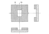
図8は、配向規制体として、対向電極に対して平面図を考えた場合の形状が円形をなすリベット95aを用いたものである。中心を通るE-E線による垂直断面図を下側に、また、中心を通るE-E線と直交するF-F線による垂直断面図を右側にそれぞれ示す。
FIG. 8 uses a rivet 95a having a circular shape when the plan view is considered with respect to the counter electrode as the orientation regulating body. A vertical sectional view taken along line EE passing through the center is shown on the lower side, and a vertical sectional view taken along line FF perpendicular to the EE line passing through the center is shown on the right side.
図9は、配向規制体として、対向電極に対して平面図を考えた場合の形状が楕円形をなすリベット95bを用いたものである。中心を通るE-E線による垂直断面図を下側に、また、中心を通るE-E線と直交するF-F線による垂直断面図を右側にそれぞれ示す。
FIG. 9 uses a rivet 95b having an elliptical shape when the plan view is taken with respect to the counter electrode as the orientation restricting body. A vertical sectional view taken along line EE passing through the center is shown on the lower side, and a vertical sectional view taken along line FF perpendicular to the EE line passing through the center is shown on the right side.
図10は、配向規制体として、対向電極に対して平面図を考えた場合の形状が矩形(正方形を含む)をなすリベット95cを用いたものである。中心を通るE-E線による垂直断面図を下側に、また、中心を通るE-E線と直交するF-F線による垂直断面図を右側にそれぞれ示す。
FIG. 10 uses a rivet 95c having a rectangular shape (including a square) when the plan view is taken with respect to the counter electrode as the orientation regulating body. A vertical sectional view taken along line EE passing through the center is shown on the lower side, and a vertical sectional view taken along line FF perpendicular to the EE line passing through the center is shown on the right side.
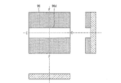
図11は、配向規制体として、対向電極に対して平面図を考えた場合の形状が直線状をなすリブ95dを用いたものである。中心を通るE-E線による垂直断面図を下側に、また、中心を通るE-E線と直交するF-F線による垂直断面図を右側にそれぞれ示す。
FIG. 11 shows a rib 95d having a linear shape when the plan view is taken with respect to the counter electrode as the orientation restricting body. A vertical sectional view taken along line EE passing through the center is shown on the lower side, and a vertical sectional view taken along line FF perpendicular to the EE line passing through the center is shown on the right side.
図12は、配向規制体として、対向電極に対して平面図を考えた場合に、透明電極96に形成された円形をなす穴96aを用いたものである。中心を通るE-E線による垂直断面図を下側に、また、中心を通るE-E線と直交するF-F線による垂直断面図を右側にそれぞれ示す。
FIG. 12 shows a case where a circular hole 96a formed in the transparent electrode 96 is used as an orientation regulating body when a plan view is considered with respect to the counter electrode. A vertical sectional view taken along line EE passing through the center is shown on the lower side, and a vertical sectional view taken along line FF perpendicular to the EE line passing through the center is shown on the right side.
図13は、配向規制体として、対向電極に対して平面図を考えた場合に、透明電極96に形成された楕円形をなす穴96bを用いたものである。中心を通るE-E線による垂直断面図を下側に、また、中心を通るE-E線と直交するF-F線による垂直断面図を右側にそれぞれ示す。
FIG. 13 shows a case where an elliptical hole 96b formed in the transparent electrode 96 is used as an orientation restricting body when a plan view is considered with respect to the counter electrode. A vertical sectional view taken along line EE passing through the center is shown on the lower side, and a vertical sectional view taken along line FF perpendicular to the EE line passing through the center is shown on the right side.
図14は、配向規制体として、対向電極に対して平面図を考えた場合に、透明電極96に形成された矩形(正方形)をなす穴96cを用いたものである。中心を通るE-E線による垂直断面図を下側に、また、中心を通るE-E線と直交するF-F線による垂直断面図を右側にそれぞれ示す。
FIG. 14 shows a case in which a rectangular (square) hole 96c formed in the transparent electrode 96 is used as an orientation regulating body when a plan view is considered with respect to the counter electrode. A vertical sectional view taken along line EE passing through the center is shown on the lower side, and a vertical sectional view taken along line FF perpendicular to the EE line passing through the center is shown on the right side.
図15は、配向規制体として、対向電極に対して平面図を考えた場合に、透明電極96に形成された直線状のスリット96dを用いたものである。中心を通るE-E線による垂直断面図を下側に、また、中心を通るE-E線と直交するF-F線による垂直断面図を右側にそれぞれ示す。
FIG. 15 shows a case in which a linear slit 96d formed in the transparent electrode 96 is used as the orientation regulating body when a plan view is considered with respect to the counter electrode. A vertical sectional view taken along line EE passing through the center is shown on the lower side, and a vertical sectional view taken along line FF perpendicular to the EE line passing through the center is shown on the right side.
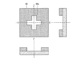
図16は、配向規制体として、対向電極に対して平面図を考えた場合に、透明電極96に形成された十字形をなす穴96eを用いたものである。中心を通るE-E線による垂直断面図を下側に、また、中心を通るE-E線と直交するF-F線による垂直断面図を右側にそれぞれ示す。
FIG. 16 shows a case where a cross-shaped hole 96e formed in the transparent electrode 96 is used as an orientation regulating body when a plan view is considered with respect to the counter electrode. A vertical sectional view taken along line EE passing through the center is shown on the lower side, and a vertical sectional view taken along line FF perpendicular to the EE line passing through the center is shown on the right side.
以上、本実施形態について述べた。本発明は、スリットを挟んで隣接する2つの反射領域の画素電極にも適用することが可能である。
The present embodiment has been described above. The present invention can also be applied to pixel electrodes in two reflection regions adjacent to each other with a slit interposed therebetween.
本発明は上述した実施形態に限定されるものではなく、請求項に示した範囲で種々の変更が可能である。すなわち、請求項に示した範囲で適宜変更した技術的手段を組み合わせて得られる実施形態についても本発明の技術的範囲に含まれる。
The present invention is not limited to the above-described embodiment, and various modifications can be made within the scope indicated in the claims. That is, embodiments obtained by combining technical means appropriately changed within the scope of the claims are also included in the technical scope of the present invention.